EP4123631B1 - Lichtemittierendes substrat und ansteuerverfahren dafür, und anzeigevorrichtung - Google Patents
Lichtemittierendes substrat und ansteuerverfahren dafür, und anzeigevorrichtung Download PDFInfo
- Publication number
- EP4123631B1 EP4123631B1 EP20925742.7A EP20925742A EP4123631B1 EP 4123631 B1 EP4123631 B1 EP 4123631B1 EP 20925742 A EP20925742 A EP 20925742A EP 4123631 B1 EP4123631 B1 EP 4123631B1
- Authority
- EP
- European Patent Office
- Prior art keywords
- light emitting
- lines
- signal
- driving
- circuit
- Prior art date
- Legal status (The legal status is an assumption and is not a legal conclusion. Google has not performed a legal analysis and makes no representation as to the accuracy of the status listed.)
- Active
Links
Images


Classifications
-
- G—PHYSICS
- G09—EDUCATION; CRYPTOGRAPHY; DISPLAY; ADVERTISING; SEALS
- G09G—ARRANGEMENTS OR CIRCUITS FOR CONTROL OF INDICATING DEVICES USING STATIC MEANS TO PRESENT VARIABLE INFORMATION
- G09G3/00—Control arrangements or circuits, of interest only in connection with visual indicators other than cathode-ray tubes
- G09G3/20—Control arrangements or circuits, of interest only in connection with visual indicators other than cathode-ray tubes for presentation of an assembly of a number of characters, e.g. a page, by composing the assembly by combination of individual elements arranged in a matrix no fixed position being assigned to or needed to be assigned to the individual characters or partial characters
- G09G3/34—Control arrangements or circuits, of interest only in connection with visual indicators other than cathode-ray tubes for presentation of an assembly of a number of characters, e.g. a page, by composing the assembly by combination of individual elements arranged in a matrix no fixed position being assigned to or needed to be assigned to the individual characters or partial characters by control of light from an independent source
- G09G3/3406—Control of illumination source
- G09G3/342—Control of illumination source using several illumination sources separately controlled corresponding to different display panel areas, e.g. along one dimension such as lines
- G09G3/3426—Control of illumination source using several illumination sources separately controlled corresponding to different display panel areas, e.g. along one dimension such as lines the different display panel areas being distributed in two dimensions, e.g. matrix
-
- G—PHYSICS
- G09—EDUCATION; CRYPTOGRAPHY; DISPLAY; ADVERTISING; SEALS
- G09G—ARRANGEMENTS OR CIRCUITS FOR CONTROL OF INDICATING DEVICES USING STATIC MEANS TO PRESENT VARIABLE INFORMATION
- G09G3/00—Control arrangements or circuits, of interest only in connection with visual indicators other than cathode-ray tubes
- G09G3/20—Control arrangements or circuits, of interest only in connection with visual indicators other than cathode-ray tubes for presentation of an assembly of a number of characters, e.g. a page, by composing the assembly by combination of individual elements arranged in a matrix no fixed position being assigned to or needed to be assigned to the individual characters or partial characters
- G09G3/22—Control arrangements or circuits, of interest only in connection with visual indicators other than cathode-ray tubes for presentation of an assembly of a number of characters, e.g. a page, by composing the assembly by combination of individual elements arranged in a matrix no fixed position being assigned to or needed to be assigned to the individual characters or partial characters using controlled light sources
- G09G3/30—Control arrangements or circuits, of interest only in connection with visual indicators other than cathode-ray tubes for presentation of an assembly of a number of characters, e.g. a page, by composing the assembly by combination of individual elements arranged in a matrix no fixed position being assigned to or needed to be assigned to the individual characters or partial characters using controlled light sources using electroluminescent panels
- G09G3/32—Control arrangements or circuits, of interest only in connection with visual indicators other than cathode-ray tubes for presentation of an assembly of a number of characters, e.g. a page, by composing the assembly by combination of individual elements arranged in a matrix no fixed position being assigned to or needed to be assigned to the individual characters or partial characters using controlled light sources using electroluminescent panels semiconductive, e.g. using light-emitting diodes [LED]
-
- G—PHYSICS
- G09—EDUCATION; CRYPTOGRAPHY; DISPLAY; ADVERTISING; SEALS
- G09G—ARRANGEMENTS OR CIRCUITS FOR CONTROL OF INDICATING DEVICES USING STATIC MEANS TO PRESENT VARIABLE INFORMATION
- G09G3/00—Control arrangements or circuits, of interest only in connection with visual indicators other than cathode-ray tubes
- G09G3/20—Control arrangements or circuits, of interest only in connection with visual indicators other than cathode-ray tubes for presentation of an assembly of a number of characters, e.g. a page, by composing the assembly by combination of individual elements arranged in a matrix no fixed position being assigned to or needed to be assigned to the individual characters or partial characters
- G09G3/2085—Special arrangements for addressing the individual elements of the matrix, other than by driving respective rows and columns in combination
- G09G3/2088—Special arrangements for addressing the individual elements of the matrix, other than by driving respective rows and columns in combination with use of a plurality of processors, each processor controlling a number of individual elements of the matrix
-
- G—PHYSICS
- G09—EDUCATION; CRYPTOGRAPHY; DISPLAY; ADVERTISING; SEALS
- G09G—ARRANGEMENTS OR CIRCUITS FOR CONTROL OF INDICATING DEVICES USING STATIC MEANS TO PRESENT VARIABLE INFORMATION
- G09G3/00—Control arrangements or circuits, of interest only in connection with visual indicators other than cathode-ray tubes
- G09G3/20—Control arrangements or circuits, of interest only in connection with visual indicators other than cathode-ray tubes for presentation of an assembly of a number of characters, e.g. a page, by composing the assembly by combination of individual elements arranged in a matrix no fixed position being assigned to or needed to be assigned to the individual characters or partial characters
- G09G3/34—Control arrangements or circuits, of interest only in connection with visual indicators other than cathode-ray tubes for presentation of an assembly of a number of characters, e.g. a page, by composing the assembly by combination of individual elements arranged in a matrix no fixed position being assigned to or needed to be assigned to the individual characters or partial characters by control of light from an independent source
- G09G3/3406—Control of illumination source
-
- G—PHYSICS
- G09—EDUCATION; CRYPTOGRAPHY; DISPLAY; ADVERTISING; SEALS
- G09G—ARRANGEMENTS OR CIRCUITS FOR CONTROL OF INDICATING DEVICES USING STATIC MEANS TO PRESENT VARIABLE INFORMATION
- G09G2300/00—Aspects of the constitution of display devices
- G09G2300/04—Structural and physical details of display devices
- G09G2300/0404—Matrix technologies
- G09G2300/0408—Integration of the drivers onto the display substrate
-
- G—PHYSICS
- G09—EDUCATION; CRYPTOGRAPHY; DISPLAY; ADVERTISING; SEALS
- G09G—ARRANGEMENTS OR CIRCUITS FOR CONTROL OF INDICATING DEVICES USING STATIC MEANS TO PRESENT VARIABLE INFORMATION
- G09G2300/00—Aspects of the constitution of display devices
- G09G2300/04—Structural and physical details of display devices
- G09G2300/0421—Structural details of the set of electrodes
- G09G2300/0426—Layout of electrodes and connections
-
- G—PHYSICS
- G09—EDUCATION; CRYPTOGRAPHY; DISPLAY; ADVERTISING; SEALS
- G09G—ARRANGEMENTS OR CIRCUITS FOR CONTROL OF INDICATING DEVICES USING STATIC MEANS TO PRESENT VARIABLE INFORMATION
- G09G2300/00—Aspects of the constitution of display devices
- G09G2300/04—Structural and physical details of display devices
- G09G2300/0439—Pixel structures
- G09G2300/0465—Improved aperture ratio, e.g. by size reduction of the pixel circuit, e.g. for improving the pixel density or the maximum displayable luminance or brightness
-
- G—PHYSICS
- G09—EDUCATION; CRYPTOGRAPHY; DISPLAY; ADVERTISING; SEALS
- G09G—ARRANGEMENTS OR CIRCUITS FOR CONTROL OF INDICATING DEVICES USING STATIC MEANS TO PRESENT VARIABLE INFORMATION
- G09G2310/00—Command of the display device
- G09G2310/02—Addressing, scanning or driving the display screen or processing steps related thereto
- G09G2310/0243—Details of the generation of driving signals
-
- G—PHYSICS
- G09—EDUCATION; CRYPTOGRAPHY; DISPLAY; ADVERTISING; SEALS
- G09G—ARRANGEMENTS OR CIRCUITS FOR CONTROL OF INDICATING DEVICES USING STATIC MEANS TO PRESENT VARIABLE INFORMATION
- G09G2310/00—Command of the display device
- G09G2310/08—Details of timing specific for flat panels, other than clock recovery
-
- G—PHYSICS
- G09—EDUCATION; CRYPTOGRAPHY; DISPLAY; ADVERTISING; SEALS
- G09G—ARRANGEMENTS OR CIRCUITS FOR CONTROL OF INDICATING DEVICES USING STATIC MEANS TO PRESENT VARIABLE INFORMATION
- G09G2320/00—Control of display operating conditions
- G09G2320/06—Adjustment of display parameters
- G09G2320/0626—Adjustment of display parameters for control of overall brightness
- G09G2320/064—Adjustment of display parameters for control of overall brightness by time modulation of the brightness of the illumination source
-
- G—PHYSICS
- G09—EDUCATION; CRYPTOGRAPHY; DISPLAY; ADVERTISING; SEALS
- G09G—ARRANGEMENTS OR CIRCUITS FOR CONTROL OF INDICATING DEVICES USING STATIC MEANS TO PRESENT VARIABLE INFORMATION
- G09G2330/00—Aspects of power supply; Aspects of display protection and defect management
- G09G2330/02—Details of power systems and of start or stop of display operation
- G09G2330/021—Power management, e.g. power saving
-
- G—PHYSICS
- G09—EDUCATION; CRYPTOGRAPHY; DISPLAY; ADVERTISING; SEALS
- G09G—ARRANGEMENTS OR CIRCUITS FOR CONTROL OF INDICATING DEVICES USING STATIC MEANS TO PRESENT VARIABLE INFORMATION
- G09G2330/00—Aspects of power supply; Aspects of display protection and defect management
- G09G2330/12—Test circuits or failure detection circuits included in a display system, as permanent part thereof
-
- G—PHYSICS
- G09—EDUCATION; CRYPTOGRAPHY; DISPLAY; ADVERTISING; SEALS
- G09G—ARRANGEMENTS OR CIRCUITS FOR CONTROL OF INDICATING DEVICES USING STATIC MEANS TO PRESENT VARIABLE INFORMATION
- G09G2370/00—Aspects of data communication
-
- G—PHYSICS
- G09—EDUCATION; CRYPTOGRAPHY; DISPLAY; ADVERTISING; SEALS
- G09G—ARRANGEMENTS OR CIRCUITS FOR CONTROL OF INDICATING DEVICES USING STATIC MEANS TO PRESENT VARIABLE INFORMATION
- G09G2370/00—Aspects of data communication
- G09G2370/02—Networking aspects
-
- G—PHYSICS
- G09—EDUCATION; CRYPTOGRAPHY; DISPLAY; ADVERTISING; SEALS
- G09G—ARRANGEMENTS OR CIRCUITS FOR CONTROL OF INDICATING DEVICES USING STATIC MEANS TO PRESENT VARIABLE INFORMATION
- G09G2370/00—Aspects of data communication
- G09G2370/04—Exchange of auxiliary data, i.e. other than image data, between monitor and graphics controller
-
- H—ELECTRICITY
- H10—SEMICONDUCTOR DEVICES; ELECTRIC SOLID-STATE DEVICES NOT OTHERWISE PROVIDED FOR
- H10W—GENERIC PACKAGES, INTERCONNECTIONS, CONNECTORS OR OTHER CONSTRUCTIONAL DETAILS OF DEVICES COVERED BY CLASS H10
- H10W90/00—Package configurations
Definitions
- Embodiments of the present disclosure relate to a light emitting substrate, a method of driving a light emitting substrate, and a display device.
- EP2713357A1 discloses a light emitting substrate, comprising a plurality of light emitting units arranged in an array, wherein each light emitting unit comprises a driving circuit, a plurality of light emitting elements, and a driving voltage terminal , the driving circuit comprises a first input terminal, a second input terminal, and an output terminal, and the plurality of light emitting elements are sequentially connected in series and connected between the driving voltage terminal and the output terminal
- connection/connecting/connected are not limited to a physical connection or mechanical connection, but may comprise an electrical connection/coupling, directly or indirectly.
- the terms, “on,” “under,” “left,” “right,” or the like are only used to indicate relative position relationship, and when the position of the object which is described is changed, the relative position relationship may be changed accordingly.
- the mini light emitting diode (mini-LED) or the micro light emitting diode (micro-LED) is small in size and high in brightness, and may be widely used in backlight modules of display devices, to finely adjust backlight, so as to implement display of high-dynamic range (HDR) images.
- a typical size (e.g., length) of a micro-LED is less than 50 microns, for example, 10 microns to 50 microns; and a typical size (e.g., length) of a mini-LED is 50 microns to 150 microns, for example, 80 microns to 120 microns.
- the light emitting diode Due to the small size of the light emitting diode, when the light emitting diode is applied to the backlight module, a huge number of light emitting diodes are required. Moreover, because the light emitting diode is a current driving element, the signal line needs to transmit a current signal from a driving chip to the light emitting diode. If it is intended to independently control each light emitting diode in the backlight module, a large number of driving chips and dense signal lines need to be arranged accordingly, which leads to higher product costs. In addition, the chip area of the driving circuit is usually large, which may take up more space, thereby increasing the difficulty in product design and processing.
- At least one embodiment of the present disclosure provides a light emitting substrate, a method of driving a light emitting substrate, and a display device.
- the light emitting substrate can implement partitioned independent control of light emission brightness with low power consumption, high integration, simple control mode, and can cooperate with a liquid crystal display device to implement high-contrast display.
- At least one embodiment of the present disclosure provides a light emitting substrate, and the light emitting substrate includes a plurality of light emitting units arranged in an array.
- Each light emitting unit includes a driving circuit, a plurality of light emitting elements, and a driving voltage terminal.
- the driving circuit includes a first input terminal, a second input terminal and an output terminal; and the plurality of light emitting elements are sequentially connected in series and connected between the driving voltage terminal and the output terminal.
- the driving circuit is configured to output a relay signal through the output terminal in a first period according to a first input signal received by the first input terminal and a second input signal received by the second input terminal, and supply a driving signal to the plurality of light emitting elements sequentially connected in series through the output terminal in a second period.
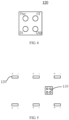
- FIG. 1 is a schematic diagram of a light emitting substrate provided by some embodiments of the present disclosure
- FIG. 2 is a schematic diagram of arrangement of light emitting units of the light emitting substrate shown in FIG. 1
- a light emitting substrate 10 includes a base substrate 01 and a plurality of light emitting units 100 arranged in an array on the base substrate 01.
- the plurality of light emitting units 100 are arranged in N rows and M columns, N is an integer greater than 0, and M is an integer greater than 0.
- the number of the light emitting units 100 may be determined according to actual needs, for example, according to the size of the light emitting substrate 10 and required brightness.
- the base substrate 01 may be a plastic substrate, a silicon substrate, a ceramic substrate, a glass substrate, a quartz substrate, etc.; and the base substrate 01 includes a single-layer or multi-layer wires, which is not limited in the embodiments of the present disclosure.
- each row of light emitting units 100 are arranged along a first direction; and each column of light emitting units 100 are arranged along a second direction.
- the first direction is a row direction and the second direction is a column direction.
- the embodiments of the present disclosure are not limited thereto, and the first direction and the second direction may be arbitrary directions, as long as the first direction and the second direction intersect with each other.
- the plurality of light emitting units 100 are not limited to being arranged along a straight line, and they may also be arranged along a curve, in a ring, or in an arbitrary manner, which may be determined according to actual needs, and is not limited in the embodiments of the present disclosure.
- FIG. 3 is a schematic diagram of a light emitting unit in the light emitting substrate shown in FIG. 1
- FIG. 4 is a schematic diagram of pins of a driving circuit in the light emitting unit of the light emitting substrate shown in FIG. 1
- each light emitting unit 100 includes a driving circuit 110, a plurality of light emitting elements 120, and a driving voltage terminal Vled.
- the driving circuit 110 includes a first input terminal Di, a second input terminal Pwr, an output terminal OT, and a common voltage terminal GND.
- the first input terminal Di receives a first input signal; and the first input signal is, for example, an address signal for turning on the driving circuit 110 of the corresponding address.
- addresses of different driving circuits 110 may be the same or different.
- the first input signal may be an 8-bit address signal, and an address to be transmitted may be obtained by parsing the address signal.
- the second input terminal Pwr receives a second input signal, and the second input signal is, for example, a power line carrier communication signal.
- the second input signal not only supplies electric power to the driving circuit 110, but also transmits communication data to the driving circuit 110, and the communication data can be used to control light emission duration of a corresponding light emitting unit 100, so as to further control visual light emission brightness thereof.
- the output terminal OT can respectively output different signals in different periods, for example, respectively output a relay signal and a driving signal.
- the relay signal is an address signal supplied to other driving circuit 110, that is, the first input terminal Di of other driving circuit 110 receives the relay signal as the first input signal, so as to acquire the address signal.
- the driving signal may be a driving current for driving the light emitting element 120 to emit light.
- the common voltage terminal GND receives a common voltage signal, for example, a ground signal.
- the driving circuit 110 is configured to output the relay signal through the output terminal OT in the first period according to the first input signal received by the first input terminal Di and the second input signal received by the second input terminal Pwr, and supply the driving signal to the plurality of light emitting elements 120 sequentially connected in series through the output terminal OT in the second period.
- the output terminal OT outputs the relay signal, and the relay signal is supplied to other driving circuit 110 so that other driving circuit 110 acquires the address signal.
- the output terminal OT outputs the driving signal, and the driving signal is supplied to the plurality of light emitting elements 120 sequentially connected in series, so that the light emitting elements 120 emit light in the second period.
- the first period and the second period are different periods, and the first period, for example, may be earlier than the second period.
- the first period may be continuously connected with the second period, and the end moment of the first period is the start moment of the second period; or, there may be other period between the first period and the second period, and the other period may be used to implement other required functions, or the other period may also be used only to separate the first period and the second period, so as to prevent signals of the output terminal OT in the first period and the second period from interfering with each other.
- the operation principle of the driving circuit 110 will be described in detail later, and no details will be repeated here.
- the driving current may flow from the output terminal OT into the light emitting element 120, or may flow from the light emitting element 120 into the output terminal OT.
- the flow direction of the driving current may be determined according to actual needs, which is not limited in the embodiments of the present disclosure.
- the expression that "the output terminal OT outputs a driving signal" indicates that the output terminal OT supplies the driving signal, and the driving signal may either flow in a direction out from the output terminal OT or flow in a direction into the output terminal OT.
- the plurality of light emitting elements 120 are sequentially connected in series and connected in series between the driving voltage terminal Vled and the output terminal OT.
- the light emitting element 120 may be a micro light emitting diode (micro-LED) or a mini light emitting diode (mini-LED).
- each light emitting element 120 includes a positive electrode (+) and a negative electrode (-) (or, which may also be referred to as an anode and a cathode); and positive electrodes and negative electrodes of the plurality of light emitting elements 120 are sequentially connected in series head to tail, so that a current path is formed between the driving voltage terminal Vled and the output terminal OT.
- the driving voltage terminal Vled supplies a driving voltage, for example, a high voltage during a period (the second period) in which the light emitting element 120 needs to emit light, and a low voltage in the other period.
- the driving signal e.g., the driving current
- the driving voltage terminal Vled sequentially through the plurality of light emitting elements 120, and then flows into the output terminal OT of the driving circuit 110.
- the plurality of light emitting elements 120 emit light when the driving current flows through; and by controlling duration of the driving current, light emission duration of the light emitting elements 120 may be controlled, thereby controlling visual light emission brightness.
- one light emitting unit 100 includes 6 light emitting elements 120, and the 6 light emitting elements 120 are arranged in 2 rows and 3 columns.
- the 6 light emitting elements 120 are sequentially numbered as (1, 1), (1, 2), (1, 3), (2, 1), (2, 2) and (2, 3) in a manner from left to right and from top to bottom, and the serial numbers are shown in FIG. 3 .
- the light emitting element 120 in position (2, 1) is used as a start point of the serial connection, and light emitting elements 120 in positions (1, 1), (2, 2), (1, 2), (2, 3) and (1, 3) are connected sequentially, with the light emitting element 120 in position (1, 3) as an end point of the serial connection.
- the positive electrode of the light emitting element 120 in position (2, 1) is connected with the driving voltage terminal Vled, and the negative electrode of the light emitting element 120 in position (1, 3) is connected with the output terminal OT of the driving circuit 110.
- Such a distribution mode and serial connection mode may effectively avoid overlapping of traces, and facilitate design and manufacturing.
- bending shapes and lengths of traces between two arbitrary adjacent light emitting elements 120 on the series path are approximately the same, so that resistance of the trace itself is relatively balanced, which can improve load balance and improve stability of the circuit.
- FIG. 5 is a schematic diagram of arrangement of light emitting elements and the driving circuit in the light emitting unit of the light emitting substrate shown in FIG. 1 .
- the plurality of (e.g., 6) light emitting elements 120 are arranged in an array, for example, arranged in a plurality of rows and a plurality of columns, so that light emission may be more uniform.
- the driving circuit 110 is located in the gap of the array constituted by the plurality of light emitting elements 120.
- the number of light emitting elements 120 in each light emitting unit 100 is not limited, and may be any number such as 4, 5, 7, 8, etc., and is not limited to 6.
- the plurality of light emitting elements 120 may be arranged in any manner, for example, in a desired pattern, and is not limited to arrangement in a matrix.
- the arrangement position of the driving circuit 110 is not limited, and the driving circuit 110 may be arranged in any gap between light emitting elements 120, which may be determined according to actual needs, and is not limited in the embodiments of the present disclosure.
- the operation principle of the driving circuit 110 is briefly described below.
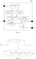
- FIG. 6A is a schematic block diagram of principle of a driving circuit in a light emitting unit of a light emitting substrate provided by some embodiments of the present disclosure.
- the driving circuit 110 includes a demodulating circuit 111, a physical layer interface circuit 112, a data processing control circuit 113, a pulse width modulating circuit 114, a driving signal generating circuit 115, a relay signal generating circuit 116, and a power supply circuit 117.
- the demodulating circuit 111 is electrically connected with the second input terminal Pwr and the physical layer interface circuit 112, and is configured to demodulate the second input signal to obtain communication data, and transmit the communication data to the physical layer interface circuit 112.
- the second input signal input by the second input terminal Pwr is a power line carrier communication signal
- the power line carrier communication signal contains information corresponding to the communication data.
- the communication data is data representing light emission duration, which in turn represents required light emission brightness.
- SPI serial peripheral interface
- PLC power line carrier communication
- FIG. 6B is a waveform diagram of the second input signal in the driving circuit shown in FIG. 6A .
- the dashed oval frame represents an enlarged view of a corresponding waveform.
- the demodulating circuit 111 filters out the direct current power component of the second input signal, so that the communication data can be obtained.
- the conventional power line carrier communication signal may be referred to, and no details will be repeated here.
- the demodulating circuit of the conventional power line carrier communication signal may also be referred to, and no details will be repeated here.
- the physical layer interface circuit 112 is also electrically connected with the data processing control circuit 113, and is configured to process the communication data to obtain a data frame (e.g., frame rate data), and transmit the data frame to the data processing control circuit 113.
- the data frame obtained by the physical layer interface circuit 112 contains information that needs to be transmitted to the driving circuit 110, for example, information related to light emission duration (e.g., specific light emission duration).
- the physical layer interface circuit 112 may be a common port physical (PHY) layer, for detailed description, the conventional design may be referred to, and no details will be repeated here.
- PHY common port physical
- the data processing control circuit 113 is also electrically connected with the first input terminal Di, the pulse width modulating circuit 114, and the relay signal generating circuit 116.
- the data processing control circuit 113 is configured to generate a pulse width control signal based on the data frame and transmit the pulse width control signal to the pulse width modulating circuit 114, and generate a relay control signal based on the first input signal and transmit the relay control signal to the relay signal generating circuit 116.
- required light emission duration of the light emitting element 120 connected with the driving circuit 110 may be known, so a corresponding pulse width control signal is generated based on the light emission duration.
- the relay control signal is a signal generated after the data processing control circuit 113 processes the first input signal.
- an address signal corresponding to the driving circuit 110 may be known, a relay control signal corresponding to a subsequent address may be generated, and the subsequent address corresponds to other driving circuit 110.
- the data processing control circuit 113 may be implemented as a single-chip microcomputer, a central processing unit (CPU), a digital signal processor, etc.
- the pulse width modulating circuit 114 is also electrically connected with the driving signal generating circuit 115, and is configured to generate a pulse width modulating signal in response to the pulse width control signal, and transmit the pulse width modulating signal to the driving signal generating circuit 115.
- the pulse width modulating signal generated by the pulse width modulating circuit 114 corresponds to the light emission duration required by the light emitting element 120, for example, effective pulse width duration is equal to the light emission duration required by the light emitting element 120.
- the conventional pulse width modulating circuit may be referred to, and no details will be repeated here.
- the driving signal generating circuit 115 is also electrically connected with the output terminal OT, and is configured to generate a driving signal in response to the pulse width modulating signal, and output the driving signal through the output terminal OT.
- outputting the driving signal through the output terminal OT may indicate that the driving signal (e.g., the driving current) flows from the output terminal OT to the light emitting element 120, or may also indicate that the driving signal (e.g., driving current) flows from the light emitting element 120 into the output terminal OT, and the specific current direction is not limited.
- the driving signal generating circuit 115 may include a current source A and a metal oxide semiconductor (MOS) field effect transistor (FET), and the metal oxide semiconductor field effect transistor is referred to as a MOS transistor.
- a control electrode of the MOS transistor receives the pulse width modulating signal transmitted by the pulse width modulating circuit 114, and is turned on or off under control of the pulse width modulating signal.
- a first electrode of the MOS transistor is connected with the output terminal OT; a second electrode of the MOS transistor is connected with a first electrode of the current source A; and a second electrode of the current source A is connected with the common voltage terminal GND to receive a common voltage.
- the current source A may be a constant current source.
- the MOS transistor When the pulse width modulating signal is at active level, the MOS transistor is turned on, and the current source A supplies a driving current through the output terminal OT. When the pulse width modulating signal is at inactive level, the MOS transistor is turned off, and the output terminal OT does not supply a driving current at this time. Active level duration of the pulse width modulating signal is equal to ON-duration of the MOS transistor; and the ON-duration of the MOS transistor is equal to duration that the output terminal OT supplies the driving current. In this way, the light emission duration of the light emitting element 120 may be further controlled, and thus the visual light emission brightness may be further controlled.
- the driving current flows from the output terminal OT into the driving circuit 110, and sequentially flows through the MOS transistor and the current source A, and then flows into a ground end (e.g., the common voltage terminal GND).
- a ground end e.g., the common voltage terminal GND.
- the driving signal generating circuit 115 may also adopt other circuit structure forms, which is not limited in the embodiments of the present disclosure.
- the relay signal generating circuit 116 is also electrically connected with the output terminal OT, and is configured to generate a relay signal based on the relay control signal, and output the relay signal through the output terminal OT.
- the relay control signal corresponds to a subsequent address
- the relay signal generated based on the relay control signal contains the subsequent address
- the subsequent address corresponds to other driving circuit 110.
- the relay signal is supplied to a first input terminal Di of a separately provided driving circuit 110; and the relay signal is input to the separately provided driving circuit 110 as the first input signal, so that the separately provided driving circuit 110 acquires the corresponding address signal.
- the relay signal generating circuit 116 may be implemented by a latch, a decoder, an encoder, etc., which is not limited in the embodiments of the present disclosure.
- the driving signal generating circuit 115 and the relay signal generating circuit 116 are both electrically connected with the output terminal OT, the driving signal generating circuit 115 and the relay signal generating circuit 116 respectively output the driving signal and the relay signal in different periods, and the driving signal and the relay signal are transmitted through the output terminal OT in a time sharing manner, so they do not affect each other.
- the power supply circuit 117 is electrically connected with the demodulating circuit 111 and the data processing control circuit 113, respectively, and is configured to receive electric energy and supply power to the data processing control circuit 113.
- the second input signal is a power line carrier communication signal.
- the direct current power component (i.e., electric energy) in the second input signal is transmitted to the power supply circuit 117, and is then supplied by the power supply circuit 117 to the data processing control circuit 113.
- the embodiments of the present disclosure are not limited thereto, and the power supply circuit 117 may also be electrically connected with other circuit in the driving circuit 110 to supply electric energy.
- the power supply circuit 117 may be implemented by a switch circuit, a voltage conversion circuit, a voltage stabilizing circuit, etc., which is not limited in the embodiments of the present disclosure.
- the driving circuit 110 may also include more circuits and components, and is not limited to the demodulating circuit 111, the physical layer interface circuit 112, the data processing control circuit 113, the pulse width modulating circuit 114, the driving signal generating circuit 115, the relay signal generating circuit 116, and the power supply circuit 117 as described above, which may be determined according to functions that need to be implemented, and may not be limited in the embodiments of the present disclosure.
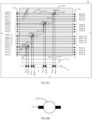
- FIG. 6C is a schematic diagram of operation flow of the driving circuit shown in FIG. 6A
- FIG. 6D is a signal timing diagram of the driving circuit shown in FIG. 6A .
- the driving circuit 110 when the driving circuit 110 is operating, it is firstly powered on (i.e., energized) to complete initialization, and then an address writing operation is performed in period S1, that is, in period S1, a first input signal Di_1 is input into the driving circuit 110 through the first input terminal Di to write an address.
- the first input signal Di_1 is sent through a separately provided transmitter.
- period S2 drive configuration is performed, and a relay signal Di_2 is output through the output terminal OT.
- the relay signal Di_2 is input as a first input signal to a first input terminal Di of a separately provided driving circuit 110.
- the foregoing first period is period S2.
- the driving voltage terminal Vled is energized.
- the driving voltage supplied by the driving voltage terminal Vled becomes a high level.
- the driving circuit 110 is in a normal operation mode, and the output terminal OT supplies a driving signal (e.g., a driving current) according to required duration, so that the light emitting elements 120 connected with the driving circuit 110 emit light according to the required duration.
- a driving signal e.g., a driving current
- the foregoing second period is period S4.
- the light emitting substrate 10 adopting the driving circuit 110 operates in a local dimming mode, which may achieve a high dynamic range effect.
- period S5 the system is shut down, that is, the driving circuit 110 is powered off, the driving voltage supplied by the driving voltage terminal Vled becomes a low level, and the light emitting elements 120 stop emitting light.
- VREG, POR, Vreg_1.8, OSC, and Reset_B are all internal signals of the driving circuit 110, which are not input or output through the first input terminal Di, the second input terminal Pwr, the output terminal OT, and the common voltage terminal GND.
- Di_1 is the first input signal received by the driving circuit 110;
- Di_2 is the relay signal output by the driving circuit 110 (i.e., the first input signal received by the next driving circuit 110 connected);
- Di_n is the first input signal received by the n- th driving circuit 110 in the plurality of driving circuits 110 sequentially connected.
- the driving circuit 110 may be implemented as a chip, with a chip size (e.g., length) of tens of microns and a chip area of about a few hundred square microns or even smaller, which is similar to a mini-LED in size, has a miniaturization characteristic, and is easy to be integrated into the light emitting substrate 10 (e.g., be soldered in the light emitting substrate 10) without being arranged outside the light emitting substrate 10 by bonding, thereby saving the arrangement space of the printed circuit board, simplifying the structure, and facilitating implementation of lightness and thinness.
- Each driving circuit 110 directly drives one light emitting unit 100, which avoids problems such as complicated operation and easy flicker in a row scanning control mode.
- the driving circuit 110 has a small number of ports, a small number of required signals, a simple control mode, a simple wiring mode, and low costs.
- the light emitting substrate 10 further includes a plurality of address transfer lines 130, and the plurality of address transfer lines 130 extend in a first direction and are configured to transmit the first input signal.
- the plurality of light emitting units 100 in the light emitting substrate 10 are arranged in N rows and M columns and are divided into a plurality of groups.
- Each group of light emitting units 100 include X rows and M columns, a total of X*M light emitting units 100; and the plurality of address transfer lines 130 are in one-to-one correspondence with the plurality of groups of light emitting units 100.
- the light emitting units 100 are divided into N/X groups. For example, in the example shown in FIG.
- each group of light emitting units 100 include 2 rows and 5 columns, a total of 10 light emitting units 100, so, every 2 rows of light emitting units 100 correspond to one address transfer line 130; and the number of address transfer lines 130 in the light emitting substrate 10 is N/2.
- N is an integer greater than
- M is an integer greater than
- 0 ⁇ X ⁇ N is an integer.
- X*M light emitting units 100 are sequentially numbered according to row and column distribution positions.
- the X*M light emitting units are sequentially numbered row by row and column by column in a Z-shape, each rectangle in FIG. 7A represents one light emitting unit 100, and the serial number of each light emitting unit 100 is marked in each rectangle.
- the X*M light emitting units are sequentially numbered row by row and column by column in an S-shape; similarly, each rectangle in FIG.
- the mode in which the light emitting units 100 are sequentially numbered according to the row and column distribution positions is not limited to the mode as described above, and they may also be numbered in other mode, so that the connection mode of the plurality of light emitting units 100 may be flexibly adjusted, which is not limited in the embodiments of the present disclosure.
- the first input terminal Di of the driving circuit 110 of the light emitting unit 100 numbered 1 is electrically connected with an address transfer line 130 corresponding to the group of light emitting units 100;
- the output terminal OT of the driving circuit 110 of the light emitting unit 100 numbered P is electrically connected with the first input terminal Di of the driving circuit 110 of the light emitting unit 100 numbered P+1;
- the first input terminal Di of the driving circuit 110 of the light emitting unit 100 numbered P+1 receives the relay signal output by the output terminal OT of the driving circuit 110 of the light emitting unit 100 numbered P as the first input signal.
- 0 ⁇ P ⁇ X*M and P is an integer.
- the first input terminal Di of the driving circuit 110 of the light emitting unit 100 located in the first row and the first column is electrically connected with the address transfer line 130 corresponding to the group of light emitting units 100; and output terminals OT of driving circuits 110 of respective light emitting units 100 are electrically connected with the first input terminal Di of the driving circuit 110 of a next light emitting unit 100 (the output terminal OT of the driving circuit 110 of the last light emitting unit 100 is not connected with other driving circuit 110).
- the first input terminal Di of the driving circuit 110 of the light emitting unit 100 located in the third row and the first column is electrically connected with the address transfer line 130 corresponding to the group of light emitting units 100; and output terminals OT of driving circuits 110 of respective light emitting units 100 are electrically connected with the first input terminal Di of the driving circuit 110 of a next light emitting unit 100, and the connection mode is similar to that of the first group of light emitting units 100.
- each group of light emitting units 100 only the first input terminal Di of the driving circuit 110 of the first light emitting unit 100 is electrically connected with the address transfer line 130, while the first input terminal Di of the driving circuit 110 of other light emitting unit 100 receives the relay signal output by the driving circuit 110 of a previous light emitting unit 100 as the first input signal. Therefore, with respect to one group of light emitting units 100, it is only necessary to supply one first input signal (i.e., the address signal) through one address transfer line 130, so that all light emitting units 100 in the group of light emitting units 100 may obtain their respective address signals. This greatly reduces the number of signal lines, saves wiring space, and simplifies the control mode.
- one first input signal i.e., the address signal
- the light emitting substrate 10 further includes a plurality of voltage transfer lines 140.
- the plurality of voltage transfer lines 140 extend along the first direction and are configured to transmit the second input signal, and the plurality of voltage transfer lines 140 are in one-to-one correspondence with N rows of light emitting units.
- each row of light emitting units 100 correspond to one voltage transfer line 140; and the number of voltage transfer lines 140 in the light emitting substrate 10 is N.
- the first row of light emitting units 100, the second row of light emitting units 100, and the third row of light emitting units 100 each correspond to one voltage transfer line 140.
- second input terminals Pwr of driving circuits 110 in the light emitting units 100 are electrically connected with a voltage transfer line 140 corresponding to the row of light emitting units 100 including the driving circuits 110. That is, second input terminals Pwr of all driving circuits 110 in a row of light emitting units 10 are electrically connected with a voltage transfer line 140 corresponding to the row so as to receive the second input signal.
- the light emitting substrate 10 further includes a plurality of source address lines 150 and a plurality of source voltage lines 160 extending in the second direction.
- the plurality of source address lines 150 are electrically connected with the plurality of address transfer lines 130 in one-to-one correspondence, and are configured to transmit the first input signal.
- the number of source address lines 150 is equal to the number of address transfer lines 130, and both are equal to N/X, that is, in the case where the light emitting units 100 are divided into N/X groups, each group of light emitting units 100 corresponds to one source address line 150 and one address transfer line 130; and the source address line 150 and the address transfer line 130 transmit the first input signal to the first light emitting unit 100 in the group of light emitting units 100.
- a source address line xAddr1 transmits a first input signal for the first group of light emitting units 100
- a source address line xAddr2 transmits a first input signal for the second group of light emitting units 100.
- the plurality of source voltage lines 160 are in one-to-one correspondence with the plurality of groups of light emitting units 100; and each source voltage line 160 is electrically connected with a plurality of voltage transfer lines 140 corresponding to a corresponding group of light emitting units 100, and is configured to transmit the second input signal.
- the number of source voltage lines 160 is N/X, that is, in the case where the light emitting units 100 are divided into N/X groups, each group of light emitting units 100 correspond to one source voltage line 160; and the source voltage line 160 transmits the second input signal to a plurality of voltage transfer lines 140 corresponding to the group of light emitting units 100, so as to supply the second input signal to all the light emitting units 100 in the group of light emitting units 100.
- a source address line 150 and a source voltage line 160 corresponding to a same group of light emitting units 100 are arranged adjacent to each other.
- the source voltage line xPwr1 is electrically connected with two voltage transfer lines 140 corresponding to the first group of light emitting units 100, so as to supply a second input signal to the first row and the second row of light emitting units 100; and the source voltage line xPwr2 is electrically connected with two voltage transfer lines 140 corresponding to the second group of light emitting units 100, so as to supply a second input signal to the third row and the fourth row of light emitting units 100 (the fourth row of light emitting units 100 and the corresponding voltage transfer line 140 are not shown in the figure).
- second input terminals Pwr of driving circuits 110 of all the light emitting units 100 are electrically connected with corresponding voltage transfer lines 140; and these voltage transfer lines 140 are connected with a same source voltage line 160. Therefore, with respect to a group of light emitting units 100, it is only necessary to supply one second input signal through one source voltage line 160, so that all the light emitting units 100 in the group of light emitting units 100 may obtain the second input signal. This greatly reduces the number of signal lines, saves wiring space, and simplifies the control mode.
- the number of source address lines 150 and the number of source voltage lines 160 are both N/X.
- the source address line 150 and the source voltage line 160 are located in a same layer; the voltage transfer line 140 and the address transfer line 130 are located in a same layer; and the source address line 150 and the address transfer line 130 are located in different layers. That is, the source address line 150 and the source voltage line 160 are manufactured by one patterning process (e.g., photoetching process); the voltage transfer line 140 and the address transfer line 130 are manufactured by another patterning process; an insulating layer is provided between the film layer where the source address line 150 and the source voltage line 160 are located and the film layer where the voltage transfer line 140 and the address transfer line 130 are located; and corresponding traces are electrically connected through a via hole penetrating through the insulating layer.
- Such mode can simplify the manufacturing process, and can be compatible with the usual semiconductor film layer manufacturing process, and improve production efficiency.
- the light emitting units 100 are divided into a plurality of groups; and light emission brightness of each group of light emitting units 100 can be separately controlled by using the above-described connection mode. For example, by setting first input signals and second input signals supplied to respective groups of light emitting units 100, light emission duration of the respective groups of light emitting units 100 is controlled, so as to further control visual light emission brightness; and the light emission duration of the respective groups of light emitting units 100 may be the same or different, which may be determined according to usage mode and needs.
- the first input signals supplied to the respective groups of light emitting units 100 are independent of each other, and the second input signals supplied to the respective groups of light emitting units 100 are independent of each other, so light emission brightness of respective groups of light emitting units 100 can be independently controlled.
- the light emitting substrate 10 can implement partitioned independent control of light emission brightness, and has a wide range of applications. In addition, the number of ports of the driving circuits 110 is small, and the number of control signals required is small, so the control mode is simple, with less power consumption, and a convenient operation.
- the light emitting substrate 10 has a high degree of integration, and may cooperate with a liquid crystal display device to implement high-contrast display.
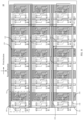
- FIG. 8A is a schematic diagram of test points of a light emitting substrate provided by some embodiments of the present disclosure.
- the light emitting substrate 10 further includes a plurality of first test points 181, a plurality of second test points 182, a plurality of third test points 183, and a plurality of fourth test points 184.
- the plurality of light emitting units 100 are mainly distributed in region Q. It should be noted that, it may be that all the light emitting units 100 are located in region Q, or that most of the light emitting units 100 are located in region Q, and the remaining light emitting units 100 are located around region Q. That is, region Q represents an approximate distribution region of a plurality of light emitting units 100 of which the number exceeds at least 70% of the total number.
- the plurality of first test points 181 each are located at one end of the source address line 150 or the source voltage line 160 away from the light emitting unit 100.
- the plurality of second test points 182 each are located at a connection position between the source address line 150 and the address transfer line 130, and located at a connection position between the source voltage line 160 and a voltage transfer line 140 having a distance farthest from the first test point 181 among the voltage transfer lines 140 connected with the source voltage line 160.
- the plurality of third test points 183 are located at both ends of the voltage transfer lines 140, and each located at an end of the address transfer line 130 away from the light emitting unit 100.
- the plurality of fourth test points 184 each are located at a connection position among connection positions between the source voltage lines 160 and the voltage transfer lines 140 except for positions where the second test points 182 are located.
- the first test points 181 are located on a first side F1 of the light emitting substrate 10; the second test points 182 and the fourth test points 184 are located in a middle region of the light emitting substrate 10; and the third test points 183 are located on a second side F2 and a third side F3 of the light emitting substrate 10.
- the address transfer line 130 and the voltage transfer line 140 are located in a same layer, the source address line 150 and the source voltage line 160 are located in a same layer, the two film layers are different layers, and corresponding traces are electrically connected through a via hole.
- the open circuit and the short circuit of the signal lines during the preparation process and before shipment may be timely and conveniently detected, so as to find out the faulty light emitting substrate as soon as possible.
- the subsequent process of the faulty light emitting substrate is no longer carried out, so as to avoid the waste of production resources, effectively monitor the corresponding backlight process and quality of the backlight product, and improve product quality.
- the respective test points may be exposed metal in a certain process stage, so as to facilitate placement of a probe (e.g., a test probe) for detection.
- the test points may be covered by a subsequent layer (e.g., an insulating layer such as a dielectric layer) and no longer exposed, or may remain exposed.
- the respective test points are electrically connected with corresponding signal lines.
- the test points and the corresponding signal lines may be formed integrally, or a separately provided conductive pattern may also be electrically connected with the signal line by welding, using conductive adhesive, etc.; and the separately provided conductive pattern serves as the test point.
- the structural form and the formation mode of the test point are not limited in the embodiments of the present disclosure.
- test point For example, voltage detection, current detection or resistance detection may be performed on the test point with a voltmeter, an ammeter, an ohmmeter or any other applicable test instrument, and with help of a probe, so as to check whether the line between two test points has an open circuit, a short circuit, etc.
- a voltmeter an ammeter, an ohmmeter or any other applicable test instrument
- a probe a probe that checks whether the line between two test points has an open circuit, a short circuit, etc.
- the conventional design may be referred to, and no details will be repeated here.
- FIG. 8B and FIG. 8C are schematic plane views of a single test point in a light emitting substrate provided by some embodiments of the present disclosure.
- a test point Te1 overlaps and is electrically connected with a signal line L1.
- the test point Te1 may be any one of the first test point 181, the second test point 182, the third test point 183, and the fourth test point 184; and the signal line L1 may be any one of the address transfer line 130, the voltage transfer line 140, the source address line 150 and the source voltage line 160.
- the shape of the test point Te1 is a circle.
- the diameter of the circle is greater than or equal to the line width of the signal line L1, thereby facilitating placement of the probe, so that the probe may be better electrically connected with the signal line L1.
- a test point Te2 overlaps and is electrically connected with a signal line L2.
- the test point Te2 may be any one of the first test point 181, the second test point 182, the third test point 183, and the fourth test point 184; and the signal line L2 may be any one of the address transfer line 130, the voltage transfer line 140, the source address line 150 and the source voltage line 160.
- the shape of the test point Te2 is a polygon, specifically, a square.
- the side length of the square is greater than or equal to the line width of the signal line L2, thereby facilitating placement of the probe, so that the probe may be better electrically connected with the signal line L2.
- shapes of respective test points are not limited to the circle and the square as described above, or may be any regular or irregular shape such as a hexagon, an ellipse, a trapezoid, a rectangle, a triangle, etc., which may be determined according to actual needs, and will not be limited in the embodiments of the present disclosure.
- the relationship between the size of the test point and the size of the signal line may also be determined according to actual needs, which will not be limited in the embodiments of the present disclosure.
- the address transfer line 130 and the voltage transfer line 140 are located in a same layer, the source address line 150 and the source voltage line 160 are located in a same layer, and the two film layers are different layers, the source address line 150 and the source voltage line 160 are manufactured by a previous process, the address transfer line 130 and the voltage transfer line 140 are formed on the source address line 150 and the source voltage line 160 by a subsequent process, there is an insulating layer between the two film layers, and the corresponding traces are electrically connected through a via hole.
- the first test point 181 and the second test point 182 can be used to detect whether there is an open circuit between the source address line 150 and the source voltage line 160.
- a test probe may be used to apply a voltage at both ends of a same source address line 150 or a same source voltage line 160, that is, to apply a voltage between the first test point 181 and the second test point 182, and meanwhile, it is tested whether there is a current between the two test points.
- a current is detected, there is no open circuit between the first test point 181 and the second test point 182, that is, there is no open circuit in the corresponding source address line 150 or source voltage line 160.
- a resistance value between the first test point 181 and the second test point 182 may also be detected. When the resistance value is infinite, it indicates that there is an open circuit between the two; and if the resistance value is within a reasonable range, it indicates that there is no open circuit between the two. For example, in some examples, a signal may be applied between the first test point Addr1_D and the second test point Addr1_U to detect whether an open circuit occurs.
- the first test point 181 and the third test point 183 may be used to test whether there is an open circuit in a line formed by the source address line 150 and the address transfer line 130, and to test whether there is an open circuit in a line formed by the source voltage line 160 and the voltage transfer line 140.
- a test probe may be used to apply a voltage at both ends of a same line, that is, a voltage is applied between one first test point 181 and one third test point 183, and meanwhile, it is tested whether there is a current between the two test points.
- a signal may be applied between the first test point Addr1_D and a third test point Addr1_L to detect whether an open circuit occurs. For example, in some examples, when an open circuit occurs between the first test point Addr1_D and the third test point Addr1_L, a signal may be applied between the first test point Addr1_D and the second test point Addr1_U, and between the second test point Addr1_U and the third test point Addr1_L, so as to detect whether there is an open circuit in the respective portions. The mode of detecting an open circuit is described above, and no details will be repeated here.
- the third test point 183 may be used to test whether there is an open circuit in the voltage transfer line 140.
- a test probe may be used to apply a voltage at both ends of a same voltage transfer line 140, that is, apply a voltage between one third test point 183 (e.g., the third test point 183 on the left side) and another third test point 183 (e.g., the third test point 183 on the right side), and meanwhile, it is tested whether there is a current between the two test points.
- a signal may be applied between a third test point Pwr1_L and a third test point Pwr1_R to detect whether an open circuit occurs. The mode of detecting an open circuit is described above, and no details will be repeated here.
- the second test point 182 and the fourth test point 184 may be used to find a location where an open circuit occurs after the address transfer line 130 and the voltage transfer line 140 are formed and an open circuit occurs.
- a test probe may be used to apply a voltage between a second test point 182 and a fourth test point 184 corresponding to a same group of light emitting units 100, and meanwhile, it is tested whether there is a current between the two test points, so as to determine which line segment has an open circuit.
- the mode of detecting an open circuit is described above, and no details will be repeated here.
- the first test point 181 may be used for detection after the source address line 150 and the source voltage line 160 are formed, and the first test point 181 may also be used for detection after the address transfer line 130 and the voltage transfer line 140 are formed.
- a test probe may be used to apply a voltage between two first test points 181, and meanwhile, it is tested whether there is a current between the two test points. When a current is detected, there is a short circuit between the two first test points 181, that is, a short circuit between the corresponding two lines. When there is no current detected, it indicates that there is no short circuit between the two first test points 181, that is, there is no short circuit between the corresponding two lines.
- a resistance value between the two first test points 181 may also be detected.
- the resistance value is infinite, it indicates that there is no short circuit between the two; and if the resistance value is within a certain range or smaller, it indicates that there is a short circuit between the two.
- a signal may be applied between the first test point Addr1_D and the first test point Pwr1_D to detect whether a short circuit occurs.
- the second test point 182 may also be used for short circuit detection, that is, a signal is applied between two second test points 182 to detect whether a short circuit occurs.
- test points are not limited, and may be determined according to actual needs. For example, it is not necessary to set test points on each signal line, but only set test points on certain signal lines which need attention, so as to simplify the manufacturing process and improve production efficiency.
- other test points may be also provided in the light emitting substrate 10 provided by the embodiments of the present disclosure, so as to meet diversified testing requirements.
- the light emitting substrate 10 further includes a flexible printed circuit (FPC) board 170.
- the flexible printed circuit board 170 overlaps and is electrically connected by bonding with the source address line 150 and the source voltage line 160.
- the first test point 181 is located on a side of the flexible printed circuit board 170 away from the light emitting unit 100.
- the flexible printed circuit board 170 is also used to bond with other components, such as a light emitting control circuit.
- the light emitting control circuit may supply a plurality of first input signals and a plurality of second input signals; and these first input signals and second input signals are transmitted to the respective source address lines 150 and source voltage lines 160 through the flexible printed circuit board 170, and further transmitted to the respective groups of light emitting units 100, so as to control the light emitting substrate 10 to emit light.
- FIG. 9 is a schematic diagram of wiring of a light emitting substrate provided by some embodiments of the present disclosure.
- the plurality of source address lines 150 and the plurality of source voltage lines 160 are alternately arranged.
- a source address line xAddr1 and a source voltage line xPwr1 on a leftmost side are used to supply a first input signal and a second input signal to the first group of light emitting units 100. Because the first group of light emitting units 100 is located on the uppermost side of the light emitting substrate, the source address line xAddr1 and the source voltage line xPwr1 are relatively long; the source address line xAddr1 is electrically connected with the address transfer line Addr1 to transmit the first input signal to the first input terminal Di of the driving circuit 110 of the first light emitting unit 100 in the group; and the source voltage line xPwr1 is electrically connected with a plurality of address transfer lines Pwr1 corresponding to the group of light emitting units 100 to transmit the second input signal to second input terminals Pwr of driving circuits 110 of all the light emitting units 100 in the group.
- the source address line xAddrn and the source voltage line xPwrn on the rightmost side are used to supply a first input signal and a second input signal to the last group of light emitting units 100. Because the last group of light emitting units 100 is located on the lowermost side of the light emitting substrate, the source address line xAddrn and the source voltage line xPwrn are relatively short; the source address line xAddrn is electrically connected with the address transfer line Addrn to transmit the first input signal to the first input terminal Di of the driving circuit 110 of the first light emitting unit 100 in the group; and the source voltage line xPwrn is electrically connected with a plurality of address transfer lines Pwrn corresponding to the group of light emitting units 100 to transmit the second input signal to second input terminals Pwr of driving circuits 110 of all the light emitting units 100 in the group.
- the leftmost source voltage line xPwr1 overlaps with all the other address transfer lines Addr2, ..., Addrn-1, Addrn except for the address transfer line Addr1, and sequentially generates capacitance Cpa_1_2, ..., Cpa_1_n-1, Cpa_1_n.
- the source voltage line xPwr2 overlaps with all the other address transfer lines Addr3, ..., Addrn-1, Addrn except for the address transfer lines Addr1 and Addr2, and sequentially generates capacitance Cpa_2_3, ..., Cpa_2_n-1, Cpa_2_n.
- the source voltage line xPwrn-1 overlaps with the address transfer line Addrn and generates capacitance Cpa_n-1_n.
- the above-described capacitance may be parasitic capacitance generated between lines, rather than a separate capacitive device.
- load of the second input signals in the plurality of source voltage lines xPwr1, xPwr2, ..., xPwrn need to be lower than a certain value; and capacitance corresponding to the second input signal needs to be as small as possible.
- capacitance generated due to the source voltage lines xPwr1, xPwr2, ..., xPwrn-1 overlapping with the address transfer lines Addr2, ..., Addrn-1, Addrn may cause additional load, which, thus, may has an additional impact on optical performance of the backlight using the light emitting substrate.
- the backlight including the light emitting substrate is usually stacked with a separately provided display panel, and the display panel is arranged on the backlight.
- the display panel usually includes a gate driving circuit.
- the gate driving circuit for example, is formed on a left side of the display panel to form a gate driver on array (GOA) circuit for supplying row scanning signals to pixels in the display panel. As shown in FIG.
- the leftmost source address line xAddr1 and source voltage line xPwr1 have relatively long lengths in the second direction, so they may affect the GOA circuit in the display panel, and cause signal crosstalk between the backlight and the display panel, which may have an additional impact on the display effect of the display device.
- FIG. 10 is a schematic diagram of wiring of another light emitting substrate provided by some embodiments of the present disclosure, and the light emitting substrate can effectively avoid the above-described problems.
- a plurality of source address lines 150 are arranged along the first direction. Lengths of the plurality of source address lines 150 along the second direction are different from each other; and between two source address lines 150 farthest apart along the first direction, a length of a source address line 150 closer to a gate driving circuit in a display panel stacked on the light emitting substrate 10 is shorter than a length of a source address line 150 farther away from the gate driving circuit.
- a plurality of source voltage lines 160 are arranged along the first direction.
- Lengths of the plurality of source voltage lines 160 along the second direction are different from each other; and between two source voltage lines 160 farthest apart along the first direction, a length of a source voltage line 160 closer to the gate driving circuit is less than a length of a source voltage line 160 farther away from the gate driving circuit.
- a source voltage line xPwr1 supplies a second input signal to light emitting units 100 in rows 1 to 4;
- a source voltage line xPwr2 supplies a second input signal to light emitting units 100 in rows 5 to 8, and so on.
- a source address line xAddr1 is connected with a first input terminal Di of a driving circuit 110 of a light emitting unit 100 in a first row and a first column; and a source address line xAddr2 is connected with a first input terminal Di of a driving circuit 110 of a light emitting unit 100 in a fifth row and a first column, and so on.
- a source address line xAddrn and a source voltage line xPwrn on the leftmost side are used to supply a first input signal and a second input signal to the last group of light emitting units 100. Because the last group of light emitting units 100 are located on the lowermost side of the light emitting substrate, the source address line xAddrn and the source voltage line xPwrn are relatively short.
- a source address line xAddr1 and a source voltage line xPwr1 on the rightmost side are used to supply a first input signal and a second input signal to the first group of light emitting units 100. Because the first group of light emitting units 100 is located on the uppermost side of the light emitting substrate, the source address line xAddr1 and the source voltage line xPwr1 are relatively long.
- the plurality of source address lines 150 are parallel to each other, and lengths of the plurality of source address lines 150 arranged sequentially along the first direction change monotonously, for example, sequentially become longer from left to right.
- the plurality of source voltage lines 160 are parallel to each other, and lengths of the plurality of source voltage lines 160 arranged sequentially in the first direction change monotonously, for example, sequentially become longer from left to right.
- the source address line 150 and the source voltage line 160 corresponding to a same group of light emitting units 100 are arranged adjacent to each other; and the source address lines 150 and the source voltage lines 160 are located in gaps of a plurality of columns of light emitting units 100.
- the source address lines 150 and the source voltage lines 160 are arranged in the gaps of the plurality of columns of light emitting units 100, instead of being arranged on the leftmost or rightmost side of the plurality of columns of light emitting units 100, which may prevent the signal in the source address lines 150 and the source voltage lines 160 from affecting the display panel stacked on the light emitting substrate 10.
- the source voltage line 160 does not overlap with any address transfer line 130. Therefore, no capacitance (e.g., parasitic capacitance) is generated between the source voltage line 160 and the address transfer line 130, and thus no additional load is caused, so that optical performance of the backlight using the light emitting substrate 10 is improved.
- capacitance e.g., parasitic capacitance
- the gate driving circuit is usually arranged on the leftmost side of the display panel, the source address line xAddrn and the source voltage line xPwrn on the leftmost side in the light emitting substrate 10 have relatively short lengths in the second direction, which, thus, has less impact on the gate driving circuit, and may reduce or avoid crosstalk between the backlight and the display panel, thereby improving the display effect of the display device.
- locations for arranging the address transfer line 130, the voltage transfer line 140, the source address line 150, and the source voltage line 160 may be changed according to needs, and are not limited to the manner shown in FIG. 9 and FIG. 10 , so as to better adapt to application scenarios and better meet application requirements.
- FIG. 11 is a schematic diagram of another light emitting substrate provided by some embodiments of the present disclosure.
- the light emitting substrate 10 further includes a plurality of first driving voltage lines 191 and a plurality of first common voltage lines 201 extending along the second direction, and further includes a plurality of second driving voltage lines 192 and a plurality of second common voltage lines 202 extending along the first direction.
- the first driving voltage line 191 is electrically connected with the driving voltage terminal Vled of each light emitting unit 100, and is configured to transmit the driving voltage.
- the second driving voltage line 192 is electrically connected with the first driving voltage line 191 and forms a grid-like trace so as to reduce transmission resistance and improve voltage consistency in the light emitting substrate 10.
- the first common voltage line 201 is electrically connected with the common voltage terminal GND of the driving circuit 110 of each light emitting unit 100, and is configured to transmit the common voltage (e.g., a ground voltage).
- the second common voltage line 202 is electrically connected with the first common voltage line 201 and forms a grid-like trace so as to reduce transmission resistance and improve voltage consistency in the light emitting substrate 10.
- the first driving voltage line 191 and the first common voltage line 201 are located in a same layer, and are located in a same layer as the source address line 150 and the source voltage line 160. Because the first driving voltage line 191, the first common voltage line 201, the source address line 150, and the source voltage line 160 all extend along the second direction, the four may be arranged in a same layer without overlapping with each other, so as to simplify the structure and simplify the manufacturing process.
- the second driving voltage line 192 and the second common voltage line 202 are located in a same layer, and are located in a same layer as the address transfer line 130 and the voltage transfer line 140. Because the second driving voltage line 192, the second common voltage line 202, the address transfer line 130, and the voltage transfer line 140 all extend along the first direction, the four may be arranged in a same layer without overlapping with each other, so as to simplify the structure and simplify the manufacturing process.
- the film layer where the first driving voltage line 191 in FIG. 11 is located is below the light emitting element 120, so, the first driving voltage line 191 may extend below a positive electrode of the light emitting element 120 and be electrically connected with the positive electrode of the light emitting element 120 through a via hole, that is, the first driving voltage line 191 transmits the driving voltage to an anode of the light emitting element 120 (i.e., to the driving voltage terminal Vled).
- a negative electrode of the light emitting element 120 overlaps with the first driving voltage line 191, yet the negative electrode of the light emitting element 120 is not electrically connected with the first driving voltage line 191 because the two are located in different layers.
- the film layer where the first common voltage line 201 is located is below the driving circuit 110, so, the first common voltage line 201 is located below the driving circuit 110 and is electrically connected with the common voltage terminal GND of the driving circuit 110 through a via hole.
- lengths and widths of the first driving voltage line 191, the second driving voltage line 192, the first common voltage line 201, and the second common voltage line 202 may be set to arbitrary values; the lengths may be the same or different, and the widths may also be the same or different, which may be determined according to actual needs, and will not be limited in the embodiments of the present disclosure.
- At least one embodiment of the present disclosure further provides a display device, and the display device includes a display panel and the light emitting substrate provided by any one of the embodiments of the present disclosure.
- the display device may implement partitioned independent control of light emission brightness with low power consumption, high integration, simple control mode, and may cooperate with a liquid crystal display device to implement high-contrast display.
- FIG. 12 is a cross-sectional schematic diagram of a display device provided by some embodiments of the present disclosure.
- a display device 20 includes a display panel 210 and a light emitting substrate 220.
- the light emitting substrate 220 may be the light emitting substrate provided by any one of the embodiments of the present disclosure, for example, the foregoing light emitting substrate 10.
- the display panel 210 has a display side P1 and a non-display side P2 opposite to the display side P1; and the light emitting substrate 220 is provided on the non-display side P2 of the display panel 210 as a backlight unit.
- the light emitting substrate 220 may serve as a surface light source to supply backlight to the display panel 210.
- the display panel 210 may be a liquid crystal display (LCD) panel, an electronic paper display panel, etc., which is not limited in the embodiments of the present disclosure.
- the display device 20 may be an LCD device, an electronic paper display device, etc., or may also be other devices having a display function, etc., which is not limited in the embodiments of the present disclosure.
- the display device 20 may be a mobile phone, a tablet personal computer, a television, a display, a laptop, a digital photo frame, a navigator, an E-book, and any other product or component having a display function, which is not limited in the embodiments of the present disclosure.
- the light emitting substrate 10 provided by the embodiments of the present disclosure may be applied to the above-described display device 20 as a backlight unit, or may be used alone as a substrate having a display function or a light emitting function, which is not limited in the embodiments of the present disclosure.
- the display device 20 may further include more components and structures, which may be determined according to actual needs, and will not be limited in the embodiments of the present disclosure.
- At least one embodiment of the present disclosure further provides a method of driving a light emitting substrate, and the light emitting substrate provided by any one of the embodiments of the present disclosure may be driven by using the method.
- the method may be used for implementing partitioned independent control of light emission brightness with simple control mode, and may cooperate with a liquid crystal display device to implement high-contrast display.
- the method includes operations below.
- a first input signal and a second input signal are supplied, so that an output terminal OT outputs a relay signal in a first period, and the output terminal OT supplies a driving signal to a plurality of light emitting elements 120 sequentially connected in series in a second period, so as to allow the plurality of light emitting elements 120 to emit light under action of the driving signal in the second period.
Landscapes
- Engineering & Computer Science (AREA)
- Physics & Mathematics (AREA)
- Computer Hardware Design (AREA)
- General Physics & Mathematics (AREA)
- Theoretical Computer Science (AREA)
- Control Of Indicators Other Than Cathode Ray Tubes (AREA)
- Devices For Indicating Variable Information By Combining Individual Elements (AREA)
- Liquid Crystal Display Device Control (AREA)
- Electroluminescent Light Sources (AREA)
- Liquid Crystal (AREA)
- Illuminated Signs And Luminous Advertising (AREA)
Claims (14)
- Ein lichtemittierendes Substrat (10), umfassend eine Vielzahl von lichtemittierenden Einheiten (100), die in einem Array angeordnet sind, wobei jede lichtemittierende Einheit (100) eine Treiberschaltung (110), eine Vielzahl von lichtemittierenden Elementen (120), und ein Treiberspannungsterminal (Vled) umfasst,die Treiberschaltung (110) ein erstes Eingangsterminal (Di), ein zweites Eingangsterminal (Pwr), und ein Ausgangsterminal (OT) umfasst, und die Vielzahl von lichtemittierenden Elementen (120) sequenziell in Reihe geschaltet und zwischen dem Treiberspannungsterminal (Vled) und dem Ausgangsterminal (OT) angeschlossen sind,die Treiberschaltung (110) konfiguriert ist, ein Relaissignal über das Ausgangsterminal (OT) in einer ersten Periode entsprechend einem von dem ersten Eingangsterminal (Di) empfangenen ersten Eingangssignal und einem von dem zweiten Eingangsterminal (Pwr) empfangenen zweiten Eingangssignal auszugeben, und ein Treibersignal an die Vielzahl von lichtemittierenden Elementen (120), die sequenziell in Reihe geschaltet sind, über das Ausgangsterminal (OT) in einer zweiten Periode zu liefern, wobei das Relaissignal ein Adresssignal ist, das an eine andere Treiberschaltung (110) geliefert wird;die Treiberschaltung (110) ferner eine Demodulationsschaltung (111), eine Schnittstellenschaltung der physischen Schicht (112), eine Datenverarbeitungssteuerschaltung (113), eine Pulsbreitenmodulationsschaltung (114), eine Treibersignalerzeugungsschaltung (115), und eine Relaissignalerzeugungsschaltung (116) umfasst;die Demodulationsschaltung (111) mit dem zweiten Eingangsterminal (Pwr) und der Schnittstellenschaltung der physischen Schicht (112) elektrisch verbunden ist, und konfiguriert ist, das zweite Eingangssignal zu demodulieren, um Kommunikationsdaten zu erhalten, und die Kommunikationsdaten an die Schnittstellenschaltung der physischen Schicht (112) zu übertragen, wobei die Kommunikationsdaten Daten sind, die die Lichtemissionsdauer darstellen;die Schnittstellenschaltung der physischen Schicht (112) auch mit der Datenverarbeitungssteuerschaltung (113) elektrisch verbunden ist, und konfiguriert ist, die Kommunikationsdaten zu verarbeiten, um einen Datenrahmen zu erhalten, und den Datenrahmen an die Datenverarbeitungssteuerschaltung (113) zu übertragen;die Datenverarbeitungssteuerschaltung (113) auch mit dem ersten Eingangsterminal (Di), der Pulsbreitenmodulationsschaltung (114), und der Relaissignalerzeugungsschaltung (116) elektrisch verbunden ist, und konfiguriert ist, ein Pulsbreitensteuersignal auf der Grundlage des Datenrahmens zu erzeugen und das Pulsbreitensteuersignal an die Pulsbreitenmodulationsschaltung (114) zu übertragen, und ein Relaissteuersignal auf der Grundlage des ersten Eingangssignals zu erzeugen und das Relaissteuersignal an die Relaissignalerzeugungsschaltung (116) zu übertragen, wobei das Relaissteuersignal ein Signal ist, das durch Parsing, Latching oder Dekodieren des ersten Eingangssignals erhalten wird;die Pulsbreitenmodulationsschaltung (114) auch mit der Treibersignalerzeugungsschaltung (115) elektrisch verbunden ist, und konfiguriert ist, ein Pulsbreitenmodulationssignal in Reaktion auf das Pulsbreitensteuersignal zu erzeugen, und das Pulsbreitenmodulationssignal an die Treibersignalerzeugungsschaltung (115) zu übertragen;die Treibersignalerzeugungsschaltung (115) auch mit dem Ausgangsterminal (OT) elektrisch verbunden ist, und konfiguriert ist, das Treibersignal in Reaktion auf das Pulsbreitenmodulationssignal zu erzeugen, und das Treibersignal über das Ausgangsterminal (OT) auszugeben; unddie Relaissignalerzeugungsschaltung (116) auch mit dem Ausgangsterminal (OT) elektrisch verbunden ist, und konfiguriert ist, das Relaissignal auf der Grundlage des Relaissteuersignals zu erzeugen, und das Relaissignal über das Ausgangsterminal (OT) auszugeben, wobei die Relaissignalerzeugungsschaltung (116) durch ein Latch, einen Decoder, oder einen Encoder implementiert ist.
- Das lichtemittierende Substrat (10) nach Anspruch 1, wobei das zweite Eingangssignal ein Powerline-Communication-Trägersignal ist, und das Powerline-Communication-Trägersignal Informationen enthält, die den Kommunikationsdaten entsprechen.
- Das lichtemittierende Substrat (10) nach Anspruch 1 oder 2, ferner umfassend eine Vielzahl von Adressübertragungsleitungen (130), wobei sich die Vielzahl von Adressübertragungsleitungen (130) in einer ersten Richtung erstrecken und konfiguriert sind, das erste Eingangssignal zu übertragen,die Vielzahl von lichtemittierenden Einheiten (100) in N Zeilen und M Spalten angeordnet und in eine Vielzahl von Gruppen unterteilt sind, wobei jede Gruppe von lichtemittierenden Einheiten (100) X Zeilen und M Spalten, insgesamt X*M lichtemittierende Einheiten (100), umfasst, und die Vielzahl von Adressübertragungsleitungen (130) in Eins-zu-eins-Entsprechung mit der Vielzahl von Gruppen von lichtemittierenden Einheiten (100) sind,in einer selben Gruppe von lichtemittierenden Einheiten (100) die X*M lichtemittierenden Einheiten (100) entsprechend Zeilen- und Spaltenverteilungspositionen sequenziell nummeriert sind, ein erstes Eingangsterminal (Di) einer Treiberschaltung (110) einer lichtemittierenden Einheit (100) mit der Nummer 1 mit einer Adressübertragungsleitung (130) elektrisch verbunden ist, die der Gruppe von lichtemittierenden Einheiten (100) entspricht, ein Ausgangsterminal (OT) einer Treiberschaltung (110) einer lichtemittierenden Einheit (100) mit der Nummer P mit einem ersten Eingangsterminal (Di) einer Treiberschaltung (110) einer lichtemittierenden Einheit (100) mit der Nummer P+1 elektrisch verbunden ist, und das erste Eingangsterminal (Di) der Treiberschaltung (110) der lichtemittierenden Einheit (100) mit der Nummer P+1 ein von dem Ausgangsterminal (OT) der Treiberschaltung (110) der lichtemittierenden Einheit (100) mit der Nummer P ausgegebenes Relaissignal als das erste Eingangssignal empfängt,N eine ganze Zahl größer als 0 ist, M eine ganze Zahl größer als 0 ist, 0<X≤N und X eine ganze Zahl ist, und 0<P<X*M und P eine ganze Zahl ist.
- Das lichtemittierende Substrat (10) nach Anspruch 3, wobei in einer selben Gruppe von lichtemittierenden Einheiten (100) die X*M lichtemittierenden Einheiten (100) zeilenweise und spaltenweise in einer Z-Form sequenziell nummeriert sind, oder zeilenweise und spaltenweise in einer S-Form sequenziell nummeriert sind.
- Das lichtemittierende Substrat (10) nach Anspruch 3 oder 4, ferner umfassend eine Vielzahl von Spannungsübertragungsleitungen (140),wobei sich die Vielzahl von Spannungsübertragungsleitungen (140) entlang der ersten Richtung erstrecken und konfiguriert sind, das zweite Eingangssignal zu übertragen, und die Vielzahl von Spannungsübertragungsleitungen (140) in Eins-zu-eins-Entsprechung mit N Reihen von lichtemittierenden Einheiten (100) sind, unddas zweite Eingangsterminal (Pwr) der Treiberschaltung (110) mit einer Spannungsübertragungsleitung (140) elektrisch verbunden ist, die der Reihe von lichtemittierenden Einheiten (100) entspricht, die die Treiberschaltung (110) umfasst.
- Das lichtemittierende Substrat (10) nach Anspruch 5, ferner umfassend eine Vielzahl von Quelladressleitungen (150) und eine Vielzahl von Quellspannungsleitungen (160), die sich in einer zweiten Richtung erstrecken,wobei die Vielzahl von Quelladressleitungen (150) mit der Vielzahl von Adressübertragungsleitungen (130) in Eins-zu-eins-Entsprechung elektrisch verbunden sind, und konfiguriert sind, das erste Eingangssignal zu übertragen,die Vielzahl von Quellspannungsleitungen (160) in Eins-zu-eins-Entsprechung mit der Vielzahl von Gruppen von lichtemittierenden Einheiten (100) sind, und jede Quellspannungsleitung (160) mit einer Vielzahl von Spannungsübertragungsleitungen (140) elektrisch verbunden ist, die einer entsprechenden Gruppe von lichtemittierenden Einheiten (100) entsprechen, und konfiguriert ist, das zweite Eingangssignal zu übertragen, unddie erste Richtung sich mit der zweiten Richtung schneidet;beispielsweise liegen die Quelladressleitungen (150) und die Quellspannungsleitungen (160) in einer selben Schicht, die Spannungsübertragungsleitungen (140) und die Adressübertragungsleitungen (130) liegen in einer selben Schicht, und die Quelladressleitungen (150) und die Adressübertragungsleitungen (130) liegen in verschiedenen Schichten;das lichtemittierende Substrat (10) ferner eine Vielzahl von ersten Testpunkten (181), eine Vielzahl von zweiten Testpunkten (182), eine Vielzahl von dritten Testpunkten (183), und eine Vielzahl von vierten Testpunkten (184) umfasst,wobei die Vielzahl von ersten Testpunkten (181) jeweils an einem Ende einer Quelladressleitung (150) oder einer Quellspannungsleitung (160) liegen, das von der lichtemittierenden Einheit (100) entfernt ist;die Vielzahl von zweiten Testpunkten (182) jeweils an einer Verbindungsposition zwischen der Quelladressleitung (150) und der Adressübertragungsleitung (130) liegen, und an einer Verbindungsposition zwischen der Quellspannungsleitung (160) und einer Spannungsübertragungsleitung (140), die einen weitesten Abstand von einem ersten Testpunkt (181) unter den mit der Quellspannungsleitung (160) verbundenen Spannungsübertragungsleitungen (140) hat;die Vielzahl von dritten Testpunkten (183) an beiden Enden der Spannungsübertragungsleitungen (140) liegen, und an einem von der lichtemittierenden Einheit (100) entfernten Ende der Adressübertragungsleitung (130); unddie Vielzahl von vierten Testpunkte (184) jeweils an einer Verbindungsposition unter den Verbindungspositionen zwischen den Quellspannungsleitungen (160) und den Spannungsübertragungsleitungen (140) liegen, mit Ausnahme der Positionen, an denen sich die zweiten Testpunkte (182) befinden.
- Das lichtemittierende Substrat (10) nach Anspruch 6, wobei die Vielzahl von Quelladressleitungen (150) entlang der ersten Richtung angeordnet sind, Längen von der Vielzahl von Quelladressleitungen (150) entlang der zweiten Richtung voneinander verschieden sind, und von zwei Quelladressleitungen (150), die entlang der ersten Richtung am weitesten voneinander entfernt sind, eine Länge einer Quelladressleitung (150), die näher an einer Gate-Treiberschaltung (110) in einer auf dem lichtemittierenden Substrat (10) gestapelten Anzeigetafel liegt, geringer ist als eine Länge einer Quelladressleitung (150), die weiter von der Gate-Treiberschaltung (110) entfernt ist; unddie Vielzahl von Quellspannungsleitungen (160) entlang der ersten Richtung angeordnet sind, Längen von der Vielzahl von Quellspannungsleitungen (160) entlang der zweiten Richtung voneinander verschieden sind, und von zwei Quellspannungsleitungen (160), die entlang der ersten Richtung am weitesten voneinander entfernt sind, eine Länge einer Quellspannungsleitung (160), die näher an der Gate-Treiberschaltung (110) liegt, kleiner ist als eine Länge einer Quellspannungsleitung (160), die weiter von der Gate-Treiberschaltung (110) entfernt ist;beispielsweise die Vielzahl von Quelladressenleitungen (150) parallel zueinander sind, und die Längen von der Vielzahl von Quelladressenleitungen (150), die sequenziell entlang der ersten Richtung angeordnet sind, sich monoton ändern; unddie Vielzahl von Quellspannungsleitungen (160) parallel zueinander sind, und die Längen von der Vielzahl von Quellspannungsleitungen (160), die sequenziell entlang der ersten Richtung angeordnet sind, sich monoton ändern;eine Quelladressleitung (150) und eine Quellspannungsleitung (160), die einer selben Gruppe von lichtemittierenden Einheiten (100) entsprechen, nebeneinander angeordnet sind;die Quellspannungsleitung (160) nicht mit der Adressübertragungsleitung (130) überlappt.
- Das lichtemittierende Substrat (10) nach Anspruch 6 oder 7, wobei die Quelladressleitungen (150) und die Quellspannungsleitungen (160) in Lücken von einer Vielzahl von Spalten von lichtemittierenden Einheiten (100) liegen.
- Das lichtemittierende Substrat (10) nach einem der Ansprüche 6 bis 8, ferner umfassend eine Vielzahl von ersten Treiberspannungsleitungen (191) und eine Vielzahl von ersten gemeinsamen Spannungsleitungen (201), die sich entlang der zweiten Richtung erstrecken,wobei die ersten Treiberspannungsleitungen (191) mit einem Treiberspannungsterminal (Vled) von jeder lichtemittierenden Einheit (100) elektrisch verbunden sind, und konfiguriert sind, eine Treiberspannung zu übertragen,die Treiberschaltung (110) ferner ein gemeinsames Spannungsterminal (GND) umfasst, und die ersten gemeinsamen Spannungsleitungen (201) mit dem gemeinsamen Spannungsterminal (GND) der Treiberschaltung (110) jeder lichtemittierenden Einheit (100) elektrisch verbunden sind, und konfiguriert sind, eine gemeinsame Spannung übertragen;beispielsweise die ersten Treiberspannungsleitungen (191) und die ersten gemeinsamen Spannungsleitungen (201) in einer selben Schicht liegen, und in einer selben Schicht wie die Quelladressleitungen (150) und die Quellspannungsleitungen (160) liegen;das lichtemittierende Substrat (10) ferner eine Vielzahl von zweiten Treiberspannungsleitungen (192) und eine Vielzahl von zweiten gemeinsamen Spannungsleitungen (202) umfasst, die sich entlang der ersten Richtung erstrecken,wobei die zweiten Treiberspannungsleitungen (192) mit den ersten Treiberspannungsleitungen (191) elektrisch verbunden sind und eine gitterartige Spur bilden, die zweiten gemeinsamen Spannungsleitungen (202) mit den ersten gemeinsamen Spannungsleitungen (201) elektrisch verbunden sind und eine gitterartige Spur bilden, unddie zweiten Treiberspannungsleitungen (192) und die zweiten gemeinsamen Spannungsleitungen (202) in einer selben Schicht liegen, und in einer selben Schicht wie die Adressübertragungsleitungen (130) und die Spannungsübertragungsleitungen (140) liegen.
- Das lichtemittierende Substrat (10) nach einem der Ansprüche 1 bis 9, wobei in einer selben lichtemittierenden Einheit (100) die Vielzahl von lichtemittierenden Elementen (120) in einem Array angeordnet sind, und die Treiberschaltung (110) in Lücken der Vielzahl von lichtemittierenden Elemente (120) liegt.
- Das lichtemittierende Substrat (10) nach einem der Ansprüche 1 bis 10, wobei die lichtemittierenden Elemente (120) Mikro-Leuchtdioden sind.
- Das lichtemittierende Substrat (10) nach Anspruch 6, ferner umfassend eine flexible Leiterplatte (170),
wobei die flexible Leiterplatte (170) die Quelladressleitungen (150) und die Quellspannungsleitungen (160) überlappt und mit diesen elektrisch verbunden ist, und die ersten Testpunkte (181) auf einer von den lichtemittierenden Einheiten (100) abgewandten Seite der flexiblen Leiterplatte (170) liegen. - Eine Anzeigevorrichtung (20), umfassend ein Anzeigetafel (210) und das lichtemittierende Substrat (220) nach einem der Ansprüche 1 bis 12,
wobei die Anzeigetafel (210) eine Anzeigeseite (P1) und eine der Anzeigeseite (P1) gegenüberliegende Nicht-Anzeigeseite (P2) aufweist, und das lichtemittierende Substrat (220) auf der Nicht-Anzeigeseite (P2) der Anzeigetafel (210) als eine Hintergrundbeleuchtungseinheit vorgesehen ist. - Ein Verfahren zum Ansteuern des lichtemittierenden Substrats (10) nach einem der Ansprüche 1 bis 12, umfassend:
Liefern des ersten Eingangssignals und des zweiten Eingangssignals, so dass das Ausgangsterminal (OT) das Relaissignal in der ersten Periode ausgibt, und das Ausgangsterminal (OT) in der zweiten Periode das Treibersignal an die Vielzahl von sequenziell in Reihe geschalteten lichtemittierenden Elementen (120) liefert, um es der Vielzahl von lichtemittierenden Elementen (120) zu ermöglichen, unter der Wirkung des Treibersignals in der zweiten Periode Licht zu emittieren.
Applications Claiming Priority (1)
| Application Number | Priority Date | Filing Date | Title |
|---|---|---|---|
| PCT/CN2020/079734 WO2021184202A1 (zh) | 2020-03-17 | 2020-03-17 | 发光基板及其驱动方法、显示装置 |
Publications (3)
| Publication Number | Publication Date |
|---|---|
| EP4123631A1 EP4123631A1 (de) | 2023-01-25 |
| EP4123631A4 EP4123631A4 (de) | 2023-02-01 |
| EP4123631B1 true EP4123631B1 (de) | 2025-06-18 |
Family
ID=77769664
Family Applications (1)
| Application Number | Title | Priority Date | Filing Date |
|---|---|---|---|
| EP20925742.7A Active EP4123631B1 (de) | 2020-03-17 | 2020-03-17 | Lichtemittierendes substrat und ansteuerverfahren dafür, und anzeigevorrichtung |
Country Status (7)
| Country | Link |
|---|---|
| US (2) | US11651743B2 (de) |
| EP (1) | EP4123631B1 (de) |
| JP (2) | JP7701275B2 (de) |
| KR (1) | KR102744355B1 (de) |
| CN (1) | CN113748453B (de) |
| TW (1) | TWI767473B (de) |
| WO (1) | WO2021184202A1 (de) |
Families Citing this family (10)
| Publication number | Priority date | Publication date | Assignee | Title |
|---|---|---|---|---|
| DE112021008165T5 (de) * | 2021-09-02 | 2024-08-08 | Boe Technology Group Co., Ltd. | Verdrahtungssubstrat, Anzeigesubstrat und Anzeigevorrichtung |
| CN116047809B (zh) * | 2021-12-10 | 2025-05-13 | Tcl华星光电技术有限公司 | 背光源以及显示装置 |
| US12142197B2 (en) * | 2021-12-30 | 2024-11-12 | BOE MLED Technology Co., Ltd. | Display panel and display apparatus |
| CN117480440A (zh) | 2022-04-28 | 2024-01-30 | 京东方科技集团股份有限公司 | 微型二极管灯板和发光装置 |
| WO2023221046A1 (zh) * | 2022-05-19 | 2023-11-23 | 京东方科技集团股份有限公司 | 布线基板及电子装置 |
| US20240312917A1 (en) * | 2022-05-20 | 2024-09-19 | Hefei BOE Ruisheng Technology Co., Ltd. | Wiring substrate and electronic device |
| CN117409663A (zh) * | 2022-07-07 | 2024-01-16 | 群创光电股份有限公司 | 背光模块及电子装置 |
| CN115084185B (zh) * | 2022-07-15 | 2025-08-22 | Tcl华星光电技术有限公司 | 发光基板及显示装置 |
| CN117809525A (zh) * | 2022-09-23 | 2024-04-02 | 京东方科技集团股份有限公司 | 模组结构和拼接显示装置 |
| EP4539033A4 (de) | 2023-01-19 | 2025-09-03 | Boe Technology Group Co Ltd | Ansteuerungschip, vorrichtung, konfigurationsverfahren, hintergrundbeleuchtungsmodul und anzeigevorrichtung |
Family Cites Families (33)
| Publication number | Priority date | Publication date | Assignee | Title |
|---|---|---|---|---|
| KR100798309B1 (ko) * | 2001-06-22 | 2008-01-28 | 엘지.필립스 엘시디 주식회사 | 액티브 매트릭스 유기 엘이디 구동회로 |
| US20030095086A1 (en) | 2001-09-21 | 2003-05-22 | Juergen Neuhaeusler | Circuit configuration for driving a set of at least one light-emitting diode |
| JP3764868B2 (ja) * | 2001-12-28 | 2006-04-12 | シャープ株式会社 | Ledディスプレイ装置 |
| GB0209502D0 (en) * | 2002-04-25 | 2002-06-05 | Cambridge Display Tech Ltd | Display driver circuits |
| JP3715967B2 (ja) * | 2002-06-26 | 2005-11-16 | キヤノン株式会社 | 駆動装置及び駆動回路及び画像表示装置 |
| GB0301623D0 (en) * | 2003-01-24 | 2003-02-26 | Koninkl Philips Electronics Nv | Electroluminescent display devices |
| WO2006106451A1 (en) * | 2005-04-04 | 2006-10-12 | Koninklijke Philips Electronics N.V. | A led display system |
| CN100553391C (zh) | 2006-03-15 | 2009-10-21 | 宏齐科技股份有限公司 | 发光二极管驱动电路及串联式发光二极管发光系统 |
| US20080068308A1 (en) | 2006-09-19 | 2008-03-20 | Komaden Corporation | Light-emitting unit system |
| KR100966374B1 (ko) * | 2007-08-27 | 2010-07-01 | 삼성엘이디 주식회사 | 백색 led를 이용한 면광원 및 이를 구비한 lcd백라이트 유닛 |
| JP5642347B2 (ja) | 2008-03-07 | 2014-12-17 | ミツミ電機株式会社 | 液晶バックライト装置 |
| JP2009294282A (ja) | 2008-06-03 | 2009-12-17 | Videocon Industries Ltd | バックライトおよび液晶ディスプレイ |
| WO2010004871A1 (ja) | 2008-07-11 | 2010-01-14 | シャープ株式会社 | バックライト駆動装置、それを備える表示装置、およびバックライト駆動方法 |
| US8773336B2 (en) * | 2008-09-05 | 2014-07-08 | Ketra, Inc. | Illumination devices and related systems and methods |
| CN201354983Y (zh) | 2009-01-16 | 2009-12-02 | 晶锜科技股份有限公司 | 直下式背光模块及其发光装置 |
| KR101020728B1 (ko) | 2009-06-08 | 2011-03-09 | 엘지이노텍 주식회사 | 발광 다이오드 구동 장치 |
| US8344659B2 (en) | 2009-11-06 | 2013-01-01 | Neofocal Systems, Inc. | System and method for lighting power and control system |
| US8289664B2 (en) * | 2010-03-08 | 2012-10-16 | Pass & Seymour, Inc. | Protective device for an electrical supply facility |
| ES2386657B1 (es) * | 2011-01-27 | 2013-07-05 | Senia Technologies, S.L. | Pantalla de video de led's. |
| EP2733691B1 (de) | 2011-07-12 | 2017-09-20 | Joled Inc. | Anzeigevorrichtung |
| JP5939930B2 (ja) * | 2011-09-21 | 2016-06-22 | キヤノン株式会社 | 光源装置 |
| KR20130049555A (ko) * | 2011-11-04 | 2013-05-14 | 삼성전자주식회사 | Led 구동 장치, led구동 방법 및 이를 적용한 디스플레이 장치 |
| JP2014186200A (ja) | 2013-03-25 | 2014-10-02 | Seiko Epson Corp | 電気光学装置、及び電子機器 |
| CN103268751B (zh) * | 2013-05-09 | 2015-10-21 | 深圳市明微电子股份有限公司 | 一种led显示装置的地址编码写入方法及系统 |
| CN103646631B (zh) * | 2013-12-25 | 2015-12-09 | 开源集成电路(苏州)有限公司 | 一种译码器、译码器系统和led显示屏控制系统 |
| CN104347034A (zh) * | 2014-11-20 | 2015-02-11 | 无锡科思电子科技有限公司 | 一种双电源led显示屏驱动电路 |
| CN105741749B (zh) * | 2014-12-08 | 2019-03-12 | 上海和辉光电有限公司 | 一种发光控制信号驱动电路以及有源矩阵式显示面板 |
| CN104570418B (zh) * | 2014-12-23 | 2018-05-11 | 上海天马微电子有限公司 | 一种液晶电子窗帘及其驱动方法 |
| US10223962B2 (en) * | 2016-03-21 | 2019-03-05 | X-Celeprint Limited | Display with fused LEDs |
| CN107331685B (zh) * | 2017-06-28 | 2020-06-12 | 上海天马微电子有限公司 | 一种显示面板及其制造方法、显示装置 |
| JP6694989B2 (ja) | 2018-06-27 | 2020-05-20 | シャープ株式会社 | 発光装置、表示装置、およびled表示装置 |
| CN109036295B (zh) * | 2018-08-09 | 2020-10-30 | 京东方科技集团股份有限公司 | 图像显示处理方法及装置、显示装置及存储介质 |
| CN109801568A (zh) | 2019-03-26 | 2019-05-24 | 大连集思特科技有限公司 | 一种led级联式透明显示屏 |
-
2020
- 2020-03-17 US US17/426,939 patent/US11651743B2/en active Active
- 2020-03-17 WO PCT/CN2020/079734 patent/WO2021184202A1/zh not_active Ceased
- 2020-03-17 KR KR1020217038187A patent/KR102744355B1/ko active Active
- 2020-03-17 EP EP20925742.7A patent/EP4123631B1/de active Active
- 2020-03-17 JP JP2021568846A patent/JP7701275B2/ja active Active
- 2020-03-17 CN CN202080000255.1A patent/CN113748453B/zh active Active
- 2020-12-24 TW TW109145945A patent/TWI767473B/zh active
-
2023
- 2023-03-13 US US18/182,478 patent/US11881184B2/en active Active
-
2025
- 2025-01-10 JP JP2025004363A patent/JP2025061218A/ja active Pending
Also Published As
| Publication number | Publication date |
|---|---|
| EP4123631A1 (de) | 2023-01-25 |
| EP4123631A4 (de) | 2023-02-01 |
| TWI767473B (zh) | 2022-06-11 |
| JP2023527096A (ja) | 2023-06-27 |
| JP7701275B2 (ja) | 2025-07-01 |
| KR20220155181A (ko) | 2022-11-22 |
| WO2021184202A1 (zh) | 2021-09-23 |
| KR102744355B1 (ko) | 2024-12-18 |
| US20230215393A1 (en) | 2023-07-06 |
| CN113748453A (zh) | 2021-12-03 |
| US11651743B2 (en) | 2023-05-16 |
| US20220319452A1 (en) | 2022-10-06 |
| JP2025061218A (ja) | 2025-04-10 |
| TW202137175A (zh) | 2021-10-01 |
| CN113748453B (zh) | 2024-01-26 |
| US11881184B2 (en) | 2024-01-23 |
Similar Documents
| Publication | Publication Date | Title |
|---|---|---|
| US11881184B2 (en) | Light emitting substrate, method of driving light emitting substrate, and display device | |
| US11791347B2 (en) | Light-emitting substrate and display device | |
| US12464874B2 (en) | Light-emitting substrate and display apparatus | |
| RU2486577C1 (ru) | Схема управления дисплеем и одноплатный модуль, включающий в себя такую схему | |
| US12557386B2 (en) | Light-emitting substrate and display device | |
| KR101340670B1 (ko) | 액정표시장치 | |
| US11411151B2 (en) | Light emitting panel and display device | |
| US20240186333A1 (en) | Light-emitting substrate and display apparatus | |
| US20260047500A1 (en) | Light-emitting substrate and display device | |
| WO2021253397A1 (zh) | 显示模组和显示装置 | |
| KR100397784B1 (ko) | 유기 이엘소자 패널과 구동 아이씨 패널의 모듈 형성 방법 |
Legal Events
| Date | Code | Title | Description |
|---|---|---|---|
| STAA | Information on the status of an ep patent application or granted ep patent |
Free format text: STATUS: THE INTERNATIONAL PUBLICATION HAS BEEN MADE |
|
| PUAI | Public reference made under article 153(3) epc to a published international application that has entered the european phase |
Free format text: ORIGINAL CODE: 0009012 |
|
| STAA | Information on the status of an ep patent application or granted ep patent |
Free format text: STATUS: REQUEST FOR EXAMINATION WAS MADE |
|
| 17P | Request for examination filed |
Effective date: 20210929 |
|
| AK | Designated contracting states |
Kind code of ref document: A1 Designated state(s): AL AT BE BG CH CY CZ DE DK EE ES FI FR GB GR HR HU IE IS IT LI LT LU LV MC MK MT NL NO PL PT RO RS SE SI SK SM TR |
|
| A4 | Supplementary search report drawn up and despatched |
Effective date: 20230105 |
|
| RIC1 | Information provided on ipc code assigned before grant |
Ipc: G09G 3/20 20060101ALI20221223BHEP Ipc: G09G 3/34 20060101ALI20221223BHEP Ipc: H01L 27/32 20060101ALI20221223BHEP Ipc: G09G 3/32 20160101AFI20221223BHEP |
|
| DAV | Request for validation of the european patent (deleted) | ||
| DAX | Request for extension of the european patent (deleted) | ||
| GRAP | Despatch of communication of intention to grant a patent |
Free format text: ORIGINAL CODE: EPIDOSNIGR1 |
|
| STAA | Information on the status of an ep patent application or granted ep patent |
Free format text: STATUS: GRANT OF PATENT IS INTENDED |
|
| RIC1 | Information provided on ipc code assigned before grant |
Ipc: G09G 3/20 20060101ALI20250120BHEP Ipc: G09G 3/34 20060101ALI20250120BHEP Ipc: G09G 3/32 20160101AFI20250120BHEP |
|
| INTG | Intention to grant announced |
Effective date: 20250130 |
|
| GRAS | Grant fee paid |
Free format text: ORIGINAL CODE: EPIDOSNIGR3 |
|
| GRAA | (expected) grant |
Free format text: ORIGINAL CODE: 0009210 |
|
| STAA | Information on the status of an ep patent application or granted ep patent |
Free format text: STATUS: THE PATENT HAS BEEN GRANTED |
|
| AK | Designated contracting states |
Kind code of ref document: B1 Designated state(s): AL AT BE BG CH CY CZ DE DK EE ES FI FR GB GR HR HU IE IS IT LI LT LU LV MC MK MT NL NO PL PT RO RS SE SI SK SM TR |
|
| REG | Reference to a national code |
Ref country code: GB Ref legal event code: FG4D |
|
| REG | Reference to a national code |
Ref country code: CH Ref legal event code: EP |
|
| REG | Reference to a national code |
Ref country code: DE Ref legal event code: R096 Ref document number: 602020053115 Country of ref document: DE |
|
| REG | Reference to a national code |
Ref country code: CH Ref legal event code: EP |
|
| REG | Reference to a national code |
Ref country code: IE Ref legal event code: FG4D |
|
| PG25 | Lapsed in a contracting state [announced via postgrant information from national office to epo] |
Ref country code: FI Free format text: LAPSE BECAUSE OF FAILURE TO SUBMIT A TRANSLATION OF THE DESCRIPTION OR TO PAY THE FEE WITHIN THE PRESCRIBED TIME-LIMIT Effective date: 20250618 |
|
| REG | Reference to a national code |
Ref country code: LT Ref legal event code: MG9D |
|
| PG25 | Lapsed in a contracting state [announced via postgrant information from national office to epo] |
Ref country code: NO Free format text: LAPSE BECAUSE OF FAILURE TO SUBMIT A TRANSLATION OF THE DESCRIPTION OR TO PAY THE FEE WITHIN THE PRESCRIBED TIME-LIMIT Effective date: 20250918 Ref country code: GR Free format text: LAPSE BECAUSE OF FAILURE TO SUBMIT A TRANSLATION OF THE DESCRIPTION OR TO PAY THE FEE WITHIN THE PRESCRIBED TIME-LIMIT Effective date: 20250919 |
|
| PG25 | Lapsed in a contracting state [announced via postgrant information from national office to epo] |
Ref country code: BG Free format text: LAPSE BECAUSE OF FAILURE TO SUBMIT A TRANSLATION OF THE DESCRIPTION OR TO PAY THE FEE WITHIN THE PRESCRIBED TIME-LIMIT Effective date: 20250618 |
|
| PG25 | Lapsed in a contracting state [announced via postgrant information from national office to epo] |
Ref country code: HR Free format text: LAPSE BECAUSE OF FAILURE TO SUBMIT A TRANSLATION OF THE DESCRIPTION OR TO PAY THE FEE WITHIN THE PRESCRIBED TIME-LIMIT Effective date: 20250618 |
|
| PG25 | Lapsed in a contracting state [announced via postgrant information from national office to epo] |
Ref country code: RS Free format text: LAPSE BECAUSE OF FAILURE TO SUBMIT A TRANSLATION OF THE DESCRIPTION OR TO PAY THE FEE WITHIN THE PRESCRIBED TIME-LIMIT Effective date: 20250918 |
|
| REG | Reference to a national code |
Ref country code: NL Ref legal event code: MP Effective date: 20250618 |
|
| PG25 | Lapsed in a contracting state [announced via postgrant information from national office to epo] |
Ref country code: LV Free format text: LAPSE BECAUSE OF FAILURE TO SUBMIT A TRANSLATION OF THE DESCRIPTION OR TO PAY THE FEE WITHIN THE PRESCRIBED TIME-LIMIT Effective date: 20250618 |
|
| PG25 | Lapsed in a contracting state [announced via postgrant information from national office to epo] |
Ref country code: NL Free format text: LAPSE BECAUSE OF FAILURE TO SUBMIT A TRANSLATION OF THE DESCRIPTION OR TO PAY THE FEE WITHIN THE PRESCRIBED TIME-LIMIT Effective date: 20250618 |
|
| PG25 | Lapsed in a contracting state [announced via postgrant information from national office to epo] |
Ref country code: PT Free format text: LAPSE BECAUSE OF FAILURE TO SUBMIT A TRANSLATION OF THE DESCRIPTION OR TO PAY THE FEE WITHIN THE PRESCRIBED TIME-LIMIT Effective date: 20251020 |
|
| REG | Reference to a national code |
Ref country code: AT Ref legal event code: MK05 Ref document number: 1804963 Country of ref document: AT Kind code of ref document: T Effective date: 20250618 |
|
| PG25 | Lapsed in a contracting state [announced via postgrant information from national office to epo] |
Ref country code: IS Free format text: LAPSE BECAUSE OF FAILURE TO SUBMIT A TRANSLATION OF THE DESCRIPTION OR TO PAY THE FEE WITHIN THE PRESCRIBED TIME-LIMIT Effective date: 20251018 |
|
| PG25 | Lapsed in a contracting state [announced via postgrant information from national office to epo] |
Ref country code: SM Free format text: LAPSE BECAUSE OF FAILURE TO SUBMIT A TRANSLATION OF THE DESCRIPTION OR TO PAY THE FEE WITHIN THE PRESCRIBED TIME-LIMIT Effective date: 20250618 Ref country code: AT Free format text: LAPSE BECAUSE OF FAILURE TO SUBMIT A TRANSLATION OF THE DESCRIPTION OR TO PAY THE FEE WITHIN THE PRESCRIBED TIME-LIMIT Effective date: 20250618 |
|
| PG25 | Lapsed in a contracting state [announced via postgrant information from national office to epo] |
Ref country code: CZ Free format text: LAPSE BECAUSE OF FAILURE TO SUBMIT A TRANSLATION OF THE DESCRIPTION OR TO PAY THE FEE WITHIN THE PRESCRIBED TIME-LIMIT Effective date: 20250618 |
|
| PG25 | Lapsed in a contracting state [announced via postgrant information from national office to epo] |
Ref country code: PL Free format text: LAPSE BECAUSE OF FAILURE TO SUBMIT A TRANSLATION OF THE DESCRIPTION OR TO PAY THE FEE WITHIN THE PRESCRIBED TIME-LIMIT Effective date: 20250618 |
|
| PG25 | Lapsed in a contracting state [announced via postgrant information from national office to epo] |
Ref country code: EE Free format text: LAPSE BECAUSE OF FAILURE TO SUBMIT A TRANSLATION OF THE DESCRIPTION OR TO PAY THE FEE WITHIN THE PRESCRIBED TIME-LIMIT Effective date: 20250618 |
|
| PG25 | Lapsed in a contracting state [announced via postgrant information from national office to epo] |
Ref country code: SK Free format text: LAPSE BECAUSE OF FAILURE TO SUBMIT A TRANSLATION OF THE DESCRIPTION OR TO PAY THE FEE WITHIN THE PRESCRIBED TIME-LIMIT Effective date: 20250618 |
|
| PG25 | Lapsed in a contracting state [announced via postgrant information from national office to epo] |
Ref country code: ES Free format text: LAPSE BECAUSE OF FAILURE TO SUBMIT A TRANSLATION OF THE DESCRIPTION OR TO PAY THE FEE WITHIN THE PRESCRIBED TIME-LIMIT Effective date: 20250618 |
|
| PG25 | Lapsed in a contracting state [announced via postgrant information from national office to epo] |
Ref country code: DK Free format text: LAPSE BECAUSE OF FAILURE TO SUBMIT A TRANSLATION OF THE DESCRIPTION OR TO PAY THE FEE WITHIN THE PRESCRIBED TIME-LIMIT Effective date: 20250618 |
|
| PGFP | Annual fee paid to national office [announced via postgrant information from national office to epo] |
Ref country code: DE Payment date: 20260319 Year of fee payment: 7 |
|
| PG25 | Lapsed in a contracting state [announced via postgrant information from national office to epo] |
Ref country code: IT Free format text: LAPSE BECAUSE OF FAILURE TO SUBMIT A TRANSLATION OF THE DESCRIPTION OR TO PAY THE FEE WITHIN THE PRESCRIBED TIME-LIMIT Effective date: 20250618 |
|
| PGFP | Annual fee paid to national office [announced via postgrant information from national office to epo] |
Ref country code: FR Payment date: 20260323 Year of fee payment: 7 |
|
| PLBE | No opposition filed within time limit |
Free format text: ORIGINAL CODE: 0009261 |
|
| STAA | Information on the status of an ep patent application or granted ep patent |
Free format text: STATUS: NO OPPOSITION FILED WITHIN TIME LIMIT |