EP4113832B1 - High-frequency amplifier, radio communication device, and radar device - Google Patents
High-frequency amplifier, radio communication device, and radar device Download PDFInfo
- Publication number
- EP4113832B1 EP4113832B1 EP20928877.8A EP20928877A EP4113832B1 EP 4113832 B1 EP4113832 B1 EP 4113832B1 EP 20928877 A EP20928877 A EP 20928877A EP 4113832 B1 EP4113832 B1 EP 4113832B1
- Authority
- EP
- European Patent Office
- Prior art keywords
- gate
- fingers
- common
- source
- transistor
- Prior art date
- Legal status (The legal status is an assumption and is not a legal conclusion. Google has not performed a legal analysis and makes no representation as to the accuracy of the status listed.)
- Active
Links
Images




Classifications
-
- H—ELECTRICITY
- H03—ELECTRONIC CIRCUITRY
- H03F—AMPLIFIERS
- H03F3/00—Amplifiers with only discharge tubes or only semiconductor devices as amplifying elements
- H03F3/189—High-frequency amplifiers, e.g. radio frequency amplifiers
- H03F3/19—High-frequency amplifiers, e.g. radio frequency amplifiers with semiconductor devices only
- H03F3/193—High-frequency amplifiers, e.g. radio frequency amplifiers with semiconductor devices only with field-effect devices
-
- H—ELECTRICITY
- H03—ELECTRONIC CIRCUITRY
- H03F—AMPLIFIERS
- H03F1/00—Details of amplifiers with only discharge tubes, only semiconductor devices or only unspecified devices as amplifying elements
- H03F1/08—Modifications of amplifiers to reduce detrimental influences of internal impedances of amplifying elements
- H03F1/22—Modifications of amplifiers to reduce detrimental influences of internal impedances of amplifying elements by use of cascode coupling, i.e. earthed cathode or emitter stage followed by earthed grid or base stage respectively
- H03F1/223—Modifications of amplifiers to reduce detrimental influences of internal impedances of amplifying elements by use of cascode coupling, i.e. earthed cathode or emitter stage followed by earthed grid or base stage respectively with MOSFET's
-
- H—ELECTRICITY
- H03—ELECTRONIC CIRCUITRY
- H03F—AMPLIFIERS
- H03F3/00—Amplifiers with only discharge tubes or only semiconductor devices as amplifying elements
- H03F3/189—High-frequency amplifiers, e.g. radio frequency amplifiers
- H03F3/19—High-frequency amplifiers, e.g. radio frequency amplifiers with semiconductor devices only
- H03F3/195—High-frequency amplifiers, e.g. radio frequency amplifiers with semiconductor devices only in integrated circuits
-
- H—ELECTRICITY
- H03—ELECTRONIC CIRCUITRY
- H03F—AMPLIFIERS
- H03F3/00—Amplifiers with only discharge tubes or only semiconductor devices as amplifying elements
- H03F3/20—Power amplifiers, e.g. Class B amplifiers, Class C amplifiers
- H03F3/24—Power amplifiers, e.g. Class B amplifiers, Class C amplifiers of transmitter output stages
- H03F3/245—Power amplifiers, e.g. Class B amplifiers, Class C amplifiers of transmitter output stages with semiconductor devices only
-
- H—ELECTRICITY
- H10—SEMICONDUCTOR DEVICES; ELECTRIC SOLID-STATE DEVICES NOT OTHERWISE PROVIDED FOR
- H10D—INORGANIC ELECTRIC SEMICONDUCTOR DEVICES
- H10D84/00—Integrated devices formed in or on semiconductor substrates that comprise only semiconducting layers, e.g. on Si wafers or on GaAs-on-Si wafers
- H10D84/80—Integrated devices formed in or on semiconductor substrates that comprise only semiconducting layers, e.g. on Si wafers or on GaAs-on-Si wafers characterised by the integration of at least one component covered by groups H10D12/00 or H10D30/00, e.g. integration of IGFETs
- H10D84/811—Combinations of field-effect devices and one or more diodes, capacitors or resistors
- H10D84/813—Combinations of field-effect devices and capacitor only
-
- H—ELECTRICITY
- H10—SEMICONDUCTOR DEVICES; ELECTRIC SOLID-STATE DEVICES NOT OTHERWISE PROVIDED FOR
- H10D—INORGANIC ELECTRIC SEMICONDUCTOR DEVICES
- H10D89/00—Aspects of integrated devices not covered by groups H10D84/00 - H10D88/00
- H10D89/10—Integrated device layouts
-
- H—ELECTRICITY
- H10—SEMICONDUCTOR DEVICES; ELECTRIC SOLID-STATE DEVICES NOT OTHERWISE PROVIDED FOR
- H10W—GENERIC PACKAGES, INTERCONNECTIONS, CONNECTORS OR OTHER CONSTRUCTIONAL DETAILS OF DEVICES COVERED BY CLASS H10
- H10W20/00—Interconnections in chips, wafers or substrates
- H10W20/20—Interconnections within wafers or substrates, e.g. through-silicon vias [TSV]
- H10W20/211—Through-semiconductor vias, e.g. TSVs
- H10W20/212—Top-view shapes or dispositions, e.g. top-view layouts of the vias
-
- H—ELECTRICITY
- H10—SEMICONDUCTOR DEVICES; ELECTRIC SOLID-STATE DEVICES NOT OTHERWISE PROVIDED FOR
- H10W—GENERIC PACKAGES, INTERCONNECTIONS, CONNECTORS OR OTHER CONSTRUCTIONAL DETAILS OF DEVICES COVERED BY CLASS H10
- H10W20/00—Interconnections in chips, wafers or substrates
- H10W20/20—Interconnections within wafers or substrates, e.g. through-silicon vias [TSV]
- H10W20/211—Through-semiconductor vias, e.g. TSVs
- H10W20/212—Top-view shapes or dispositions, e.g. top-view layouts of the vias
- H10W20/2125—Top-view shapes
-
- H—ELECTRICITY
- H10—SEMICONDUCTOR DEVICES; ELECTRIC SOLID-STATE DEVICES NOT OTHERWISE PROVIDED FOR
- H10W—GENERIC PACKAGES, INTERCONNECTIONS, CONNECTORS OR OTHER CONSTRUCTIONAL DETAILS OF DEVICES COVERED BY CLASS H10
- H10W20/00—Interconnections in chips, wafers or substrates
- H10W20/40—Interconnections external to wafers or substrates, e.g. back-end-of-line [BEOL] metallisations or vias connecting to gate electrodes
- H10W20/482—Interconnections external to wafers or substrates, e.g. back-end-of-line [BEOL] metallisations or vias connecting to gate electrodes for individual devices provided for in groups H10D8/00 - H10D48/00, e.g. for power transistors
- H10W20/483—Interconnections over air gaps, e.g. air bridges
-
- H—ELECTRICITY
- H10—SEMICONDUCTOR DEVICES; ELECTRIC SOLID-STATE DEVICES NOT OTHERWISE PROVIDED FOR
- H10W—GENERIC PACKAGES, INTERCONNECTIONS, CONNECTORS OR OTHER CONSTRUCTIONAL DETAILS OF DEVICES COVERED BY CLASS H10
- H10W20/00—Interconnections in chips, wafers or substrates
- H10W20/40—Interconnections external to wafers or substrates, e.g. back-end-of-line [BEOL] metallisations or vias connecting to gate electrodes
- H10W20/482—Interconnections external to wafers or substrates, e.g. back-end-of-line [BEOL] metallisations or vias connecting to gate electrodes for individual devices provided for in groups H10D8/00 - H10D48/00, e.g. for power transistors
- H10W20/484—Interconnections having extended contours, e.g. pads having mesh shape or interconnections comprising connected parallel stripes
-
- H—ELECTRICITY
- H10—SEMICONDUCTOR DEVICES; ELECTRIC SOLID-STATE DEVICES NOT OTHERWISE PROVIDED FOR
- H10W—GENERIC PACKAGES, INTERCONNECTIONS, CONNECTORS OR OTHER CONSTRUCTIONAL DETAILS OF DEVICES COVERED BY CLASS H10
- H10W20/00—Interconnections in chips, wafers or substrates
- H10W20/40—Interconnections external to wafers or substrates, e.g. back-end-of-line [BEOL] metallisations or vias connecting to gate electrodes
- H10W20/495—Capacitive arrangements or effects of, or between wiring layers
- H10W20/496—Capacitor integral with wiring layers
-
- H—ELECTRICITY
- H10—SEMICONDUCTOR DEVICES; ELECTRIC SOLID-STATE DEVICES NOT OTHERWISE PROVIDED FOR
- H10W—GENERIC PACKAGES, INTERCONNECTIONS, CONNECTORS OR OTHER CONSTRUCTIONAL DETAILS OF DEVICES COVERED BY CLASS H10
- H10W44/00—Electrical arrangements for controlling or matching impedance
- H10W44/20—Electrical arrangements for controlling or matching impedance at high-frequency [HF] or radio frequency [RF]
-
- H—ELECTRICITY
- H03—ELECTRONIC CIRCUITRY
- H03F—AMPLIFIERS
- H03F2200/00—Indexing scheme relating to amplifiers
- H03F2200/451—Indexing scheme relating to amplifiers the amplifier being a radio frequency amplifier
-
- H—ELECTRICITY
- H10—SEMICONDUCTOR DEVICES; ELECTRIC SOLID-STATE DEVICES NOT OTHERWISE PROVIDED FOR
- H10W—GENERIC PACKAGES, INTERCONNECTIONS, CONNECTORS OR OTHER CONSTRUCTIONAL DETAILS OF DEVICES COVERED BY CLASS H10
- H10W20/00—Interconnections in chips, wafers or substrates
- H10W20/20—Interconnections within wafers or substrates, e.g. through-silicon vias [TSV]
Definitions
- the present disclosure relates to a high-frequency amplifier that amplifies a signal, a radio communication device including the high-frequency amplifier, and a radar device including the high-frequency amplifier.
- the radio communication device and the radar device each include a high-frequency amplifier that amplifies a high-frequency signal.
- the high-frequency amplifier includes, for example, a common-source multi-finger field effect transistor (FET), and the common-source FET amplifies a high-frequency signal.
- FET common-source multi-finger field effect transistor
- An output power of the high-frequency amplifier increases with an increase in voltage applied to the drain of the FET.
- the FET has a withstand voltage, the drain voltage of the FET is limited.
- Patent Literature 1 discloses a high-frequency amplifier in which a drain of a common-source FET is connected to a source of a common-gate FET whose gate is grounded via a capacitor.
- a plurality of gate fingers included in the common-gate FET are bundled by a gate bus bar.
- One end of the capacitor is connected to the gate bus bar, and the other end of the capacitor is grounded.
- Patent Literature 1 WO 2014-073091
- Patent Literature 1 discloses in one embodiment a high-frequency amplifier comprising:
- the present disclosure has been made to solve the above problems, and an object of the present disclosure is to obtain a high-frequency amplifier capable of suppressing an imbalance between amplification operations of a plurality of gate fingers.
- the high-frequency amplifier is configured in such a way that the capacitors are arranged at respective positions where the impedances obtained by looking toward the capacitors from the respective gate fingers of the common-gate transistor are equal to each other.
- the high-frequency amplifier according to the present disclosure can reduce the imbalance between the amplification operations of the gate fingers.
- FIG. 1 is a configuration diagram illustrating a radio communication device including a high-frequency amplifier 1 according to a first embodiment.
- the high-frequency amplifier 1 included in the radio communication device illustrated in FIG. 1 amplifies a high-frequency signal as a signal to be amplified, and outputs the amplified high-frequency signal to a transmission antenna 2.
- the transmission antenna 2 radiates a radio wave related to the high-frequency signal output from the high-frequency amplifier 1 into space.
- FIG. 2 is a configuration diagram illustrating a radar device including the high-frequency amplifier 1 according to the first embodiment.
- the high-frequency amplifier 1 included in the radar device illustrated in FIG. 2 amplifies a radar signal as a signal to be amplified, and outputs the amplified radar signal to a transmission antenna 3.
- the transmission antenna 3 radiates a radio wave related to the radar signal output from the high-frequency amplifier 1 into space.
- FIG. 3 is a configuration diagram illustrating the high-frequency amplifier 1 according to the first embodiment.
- a signal input terminal 11 is a terminal to which a high-frequency signal, a radar signal, or a reception signal is applied as a signal to be amplified, from the outside.
- a high-frequency signal is applied to the signal input terminal 11.
- the signal input terminal 11 is connected to an input-side matching circuit.
- a common-source transistor 12 includes a gate electrode 12a, a drain electrode 12b, and a source electrode 12c.
- the gate electrode 12a of the common-source transistor 12 is connected to the signal input terminal 11.
- the drain electrode 12b of the common-source transistor 12 is connected to a source electrode 32a of a common-gate transistor 32 to be described later.
- the source electrode 12c of the common-source transistor 12 is connected to the ground.
- the common-source transistor 12 amplifies a high-frequency signal applied to the gate electrode 12a, and outputs the amplified high-frequency signal from the drain electrode 12b to the source electrode 32a of the common-gate transistor 32.
- the common-source transistor 12 for example, a GaN multi-finger transistor made of gallium nitride (GaN) formed on a monolithic microwave integrated circuit (MMIC) is used.
- GaN gallium nitride
- MMIC monolithic microwave integrated circuit
- the gate electrode 12a includes a gate bus bar 13 and gate fingers 14-1 to 14-8.
- the gate electrode 12a includes eight gate fingers 14-1 to 14-8.
- the gate electrode 12a is only required to have a plurality of gate fingers 14, and is not limited to a gate electrode having the eight gate fingers 14-1 to 14-8.
- the gate bus bar 13 is connected to the signal input terminal 11.
- One end of each of the gate fingers 14-1 to 14-8 is connected to the gate bus bar 13.
- the drain electrode 12b includes drain fingers 15-1 to 15-4.
- the drain finger 15-1 is disposed between the gate finger 14-1 and the gate finger 14-2 in parallel with each of the gate fingers 14-1 and 14-2.
- the drain finger 15-2 is disposed between the gate finger 14-3 and the gate finger 14-4 in parallel with each of the gate fingers 14-3 and 14-4.
- the drain finger 15-3 is disposed between the gate finger 14-5 and the gate finger 14-6 in parallel with each of the gate fingers 14-5 and 14-6.
- the drain finger 15-4 is disposed between the gate finger 14-7 and the gate finger 14-8 in parallel with each of the gate fingers 14-7 and 14-8.
- the source electrode 12c includes source fingers 16-1 to 16-5.
- the source finger 16-1 is disposed on the left of the gate finger 14-1 in FIG. 3 in parallel with the gate finger 14-1.
- the source finger 16-2 is disposed between the gate finger 14-2 and the gate finger 14-3 in parallel with each of the gate fingers 14-2 and 14-3.
- the source finger 16-3 is disposed between the gate finger 14-4 and the gate finger 14-5 in parallel with each of the gate fingers 14-4 and 14-5.
- the source finger 16-4 is disposed between the gate finger 14-6 and the gate finger 14-7 in parallel with each of the gate fingers 14-6 and 14-7.
- the source finger 16-5 is disposed on the right of the gate finger 14-8 in FIG. 3 in parallel with the gate finger 14-8.
- One end of the via hole 17-n is connected to the source finger 16-n, and the other end of the via hole 17-n is connected to the ground.
- a bus bar 18 is connected to the drain fingers 15-1 to 15-4 of the common-source transistor 12, and is also connected to source fingers 33-1 to 33-8 of the common-gate transistor 32.
- a gate terminal 31 includes gate terminals 31-1 and 31-2.
- the gate terminal 31 is a terminal to which a gate bias is applied.
- Each of the gate terminals 31-1 and 31-2 is connected to a gate bus bar 38 to be described later.
- the common-gate transistor 32 includes the source electrode 32a, a drain electrode 32b, and a gate electrode 32c.
- the source electrode 32a of the common-gate transistor 32 is connected to the drain electrode 12b of the common-source transistor 12.
- the drain electrode 32b of the common-gate transistor 32 is connected to a signal output terminal 37 to be described later.
- the gate electrode 32c of the common-gate transistor 32 is connected to the gate terminal 31 and a capacitor 39.
- the capacitor 39 is any one of capacitors 39-1 to 39-8 to be described later.
- the common-gate transistor 32 amplifies a high-frequency signal output from the drain electrode 12b of the common-source transistor 12, and outputs the amplified high-frequency signal from the drain electrode 32b to the signal output terminal 37.
- the common-gate transistor 32 for example, a GaN multi-finger transistor made of GaN formed on the MMIC is used.
- the source electrode 32a includes the source fingers 33-1 to 33-8.
- One end of each of the source fingers 33-1 to 33-8 is connected to the bus bar 18.
- the drain electrode 32b includes drain fingers 34-1 to 34-4.
- drain fingers 34-1 to 34-4 One end of each of the drain fingers 34-1 to 34-4 is connected to a drain bus bar 36 to be described later.
- the drain finger 34-1 is disposed between a gate finger 35-1 to be described later and a gate finger 35-2 to be described later in parallel with each of the gate fingers 35-1 and 35-2.
- the drain finger 34-2 is disposed between a gate finger 35-3 to be described later and a gate finger 35-4 to be described later in parallel with each of the gate fingers 35-3 and 35-4.
- the drain finger 34-3 is disposed between a gate finger 35-5 to be described later and a gate finger 35-6 to be described later in parallel with each of the gate fingers 35-5 and 35-6.
- the drain finger 34-4 is disposed between a gate finger 35-7 to be described later and a gate finger 35-8 to be described later in parallel with each of the gate fingers 35-7 and 35-8.
- the gate electrode 32c includes the gate fingers 35-1 to 35-8.
- One end of each of the gate fingers 35-1 to 35-8 is connected to the gate bus bar 38.
- the gate finger 35-1 is disposed between the source finger 33-1 and the drain finger 34-1 in parallel with each of the source finger 33-1 and the drain finger 34-1.
- the gate finger 35-2 is disposed between the drain finger 34-1 and the source finger 33-2 in parallel with each of the drain finger 34-1 and the source finger 33-2.
- the gate finger 35-3 is disposed between the source finger 33-3 and the drain finger 34-2 in parallel with each of the source finger 33-3 and the drain finger 34-2.
- the gate finger 35-4 is disposed between the drain finger 34-2 and the source finger 33-4 in parallel with each of the drain finger 34-2 and the source finger 33-4.
- the gate finger 35-5 is disposed between the source finger 33-5 and the drain finger 34-3 in parallel with each of the source finger 33-5 and the drain finger 34-3.
- the gate finger 35-6 is disposed between the drain finger 34-3 and the source finger 33-6 in parallel with each of the drain finger 34-3 and the source finger 33-6.
- the gate finger 35-7 is disposed between the source finger 33-7 and the drain finger 34-4 in parallel with each of the source finger 33-7 and the drain finger 34-4.
- the gate finger 35-8 is disposed between the drain finger 34-4 and the source finger 33-8 in parallel with each of the drain finger 34-4 and the source finger 33-8.
- the drain bus bar 36 is connected to each of the drain fingers 34-1 to 34-4 and the signal output terminal 37.
- the signal output terminal 37 is connected to the drain bus bar 36.
- the signal output terminal 37 is a terminal for outputting the high-frequency signal amplified by the common-gate transistor 32 to the outside.
- the signal output terminal 37 is connected to an output-side matching circuit.
- the gate bus bar 38 is connected to each of the gate terminals 31-1 and 31-2, the gate fingers 35-1 to 35-8, and the capacitors 39-1 to 39-8 to be described later.
- One end of each of the capacitors 39-1 to 39-8 is connected to the gate bus bar 38.
- each of the capacitors 39-1 to 39-8 is connected to the ground.
- the capacitor 39-1 is provided on the source finger 16-1.
- the capacitor 39-2 is provided on the source finger 16-2, and the capacitor 39-3 is also provided on the source finger 16-2.
- the capacitor 39-4 is provided on the source finger 16-3, and the capacitor 39-5 is also provided on the source finger 16-3.
- the capacitor 39-6 is provided on the source finger 16-4, and the capacitor 39-7 is also provided on the source finger 16-4.
- the capacitor 39-8 is provided on the source finger 16-5.
- the impedance obtained by looking toward the capacitor 39 is a combined impedance obtained by looking toward all the capacitors 39-1 to 39-8.
- the capacitors 39-1 to 39-8 are arranged at positions where distances Lm from the respective gate fingers 35-m of the common-gate transistor 32 to one capacitor 39-m related to the respective gate fingers 35-m of the common-gate transistor 32 among the capacitors 39-1 to 39-8 are the same as each other.
- one related capacitor 39-m is a capacitor that has a correspondence relationship with the gate finger 35-m, that is, a capacitor closest to the gate finger 35-m. That is, among the capacitors 39-1 to 39-8, the capacitor related to the gate finger 35-m is the capacitor 39-m.
- the impedance obtained by looking toward the capacitor 39 includes the impedance of the capacitor 39.
- a direct-current drain voltage is applied to the signal output terminal 37 in order to enable both the common-source transistor 12 and the common-gate transistor 32 to operate.
- a direct-current gate voltage is applied to the signal input terminal 11.
- a direct-current gate voltage is applied to the gate terminal 31, which is one of the gate terminal 31-1 and the gate terminal 31-2.
- the high-frequency signal When a high-frequency signal is applied to the signal input terminal 11 as a signal to be amplified, the high-frequency signal is distributed to the gate fingers 14-1 to 14-8 by the gate bus bar 13.
- the common-source transistor 12 amplifies each of the high frequency signals.
- the common-source transistor 12 then outputs the amplified high-frequency signals to the drain fingers 15-1 to 15-4.
- the amplified high-frequency signals output to the drain fingers 15-1 to 15-4 are distributed to the source fingers 33-1 to 33-8 by the bus bar 18.
- the common-gate transistor 32 amplifies each of the high frequency signals.
- the common-gate transistor 32 then outputs the amplified high-frequency signals to the drain fingers 34-1 to 34-4.
- capacitances C1 to C8 of the capacitors 39-1 to 39-8 are set in such a way that the voltage amplitude between the gate electrode 12a and the source electrode 12c in the common-source transistor 12 is equal to the voltage amplitude between the gate electrode 32c and the source electrode 32a.
- the capacitances C1 to C8 of the capacitors 39-1 to 39-8 are set as described above, the common-source transistor 12 and the common-gate transistor 32 ideally operate in phase and with the same amplitude.
- the high-frequency amplifier 1 in a case where the common-source transistor 12 and the common-gate transistor 32 operate in phase and with the same amplitude can apply a drain voltage twice as high as that of a high-frequency amplifier including only one common-source transistor to the signal output terminal 37. Therefore, the high-frequency amplifier 1 in the case of operating in phase and with the same amplitude can obtain output power twice as large as the high-frequency amplifier including only one common-source transistor.
- the capacitors 39-1 to 39-8 are arranged at positions where the distances Lm from the gate finger 35-m to the capacitor 39-m are the same as each other. As illustrated in FIG. 5 , the impedances obtained by looking toward the capacitor 39-m from the gate finger 35-m are equal to each other.
- the imbalance between the amplification operations of the gate fingers 35-1 to 35-8 is eliminated.
- the combined loss of the high-frequency signals amplified by the gate fingers 35-1 to 35-8 is reduced.
- an arrow indicates a portion constituting the parasitic impedance between the gate finger 35-m and the capacitor 39-m.
- the impedances obtained by looking toward the capacitor 39-m from the gate fingers 35-m are substantially equal to each other.
- the impedances obtained by looking toward the capacitor 39-m from the gate fingers 35-m may be shifted from each other within a range that does not cause a practical problem. If each impedance is a shift that causes a phase shift of, for example, about ⁇ 2° or less with respect to an operation frequency, there is no practical problem.
- capacitors 39-1 to 39-8 are connected to the gate bus bar 38.
- FIG. 6 is a configuration diagram illustrating another high-frequency amplifier 1 according to the first embodiment.
- the capacitor 39-11 is a capacitor obtained by combining the capacitor 39-2 and the capacitor 39-3, and is related to each of the gate finger 35-2 and the gate finger 35-3.
- the capacitor 39-12 is a capacitor obtained by combining the capacitor 39-4 and the capacitor 39-5, and is related to each of the gate finger 35-4 and the gate finger 35-5.
- the capacitor 39-13 is a capacitor obtained by combining the capacitor 39-6 and the capacitor 39-7, and is related to each of the gate finger 35-6 and the gate finger 35-7.
- the capacitance C1 of the capacitor 39-1 and the capacitance C8 of the capacitor 39-8 are each half the capacitance C11, C12, or C13.
- the capacitance C1 of the capacitor 39-1 and the capacitance C8 of the capacitor 39-8 are not limited to half of the capacitance C11, C12, or C13.
- the high-frequency signals provided from the drain fingers 15-1 to 15-4 of the common-source transistor 12 to the source fingers 33-1 to 33-8 of the common-gate transistor 32 may not be completely in phase.
- the impedances obtained by looking toward the signal output terminal 37 from the respective gate fingers 35-1 to 35-8 of the common-gate transistor 32 may not be equal to each other.
- the imbalance between the amplification operations of the gate fingers 35-1 to 35-8 is eliminated.
- the imbalance is eliminated if the capacitance C1 of the capacitor 39-1 and the capacitance C8 of the capacitor 39-8 are made to be smaller than half of the capacitance C11, C12, or C13.
- the high-frequency amplifier 1 also includes the gate bus bar 38 connected to the gate fingers 35-1 to 35-8 of the common-gate transistor 32, and the capacitors 39-1 to 39-8 each of which has one end connected to the gate bus bar 38 and the other end grounded.
- the high-frequency amplifier 1 is configured in such a way that the capacitors 39-1 to 39-8 are arranged at positions where the impedances obtained by looking toward the capacitor 39 from the respective gate fingers 35-m of the common-gate transistor 32 are equal to each other. As a result, the high-frequency amplifier 1 can reduce the imbalance between the amplification operations of the gate fingers 35-1 to 35-8.
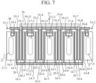
- the common-source transistor 12 and the common-gate transistor 32 are separate transistors. However, this is only an example, and for example, as illustrated in FIG. 7 , it is possible to use a dual gate transistor in which the common-source transistor 12 and the common-gate transistor 32 are implemented in one transistor cell.
- FIG. 7 is a configuration diagram illustrating still another high-frequency amplifier 1 according to the first embodiment.
- the high-frequency amplifier 1 illustrated in FIG. 7 includes drain source fingers 20-1 to 20-8.
- the drain source fingers 20-1 to 20-8 are fingers in which the drain fingers 15-1 to 15-4 of the common-source transistor 12 and the source fingers 33-1 to 33-8 of the common-gate transistor 32 are integrated.
- the gate fingers 14-1 to 14-8, the source fingers 16-1 to 16-5, the drain source fingers 20-1 to 20-8, the drain fingers 34-1 to 34-4, and the gate fingers 35-1 to 35-8 are arranged in parallel with each other.
- the high-frequency amplifier 1 illustrated in FIG. 7 includes the capacitors 39-1, 39-8, 39-11, 39-12, and 39-13 similarly to the high-frequency amplifier 1 illustrated in FIG. 6 , but does include the capacitors 39-1 to 39-8 similarly to the high-frequency amplifier 1 illustrated in FIG. 3 .
- the common-source transistor 12 and the common-gate transistor 32 are implemented as a dual gate transistor, a high-frequency amplifier having a higher frequency or a wider band than the high-frequency amplifiers 1 illustrated in FIGS. 3 and 6 can be implemented.
- the drain source fingers 20-1 to 20-8 may be omitted.
- each of the capacitors 39-1, 39-8, 39-11, 39-12, and 39-13 is connected to the gate bus bar 38.
- one end of each of the capacitors 39-1 to 39-8 is connected to the gate bus bar 38.
- one end of the capacitor 39-m may be connected to each gate finger 35-m of the common-gate transistor 32 via an air bridge 40-m.
- FIG. 8 is a configuration diagram illustrating yet another high-frequency amplifier 1 according to the first embodiment.
- FIG. 9 is a cross-sectional view taken along line A 1 -A 2 in FIG. 8 .
- the parasitic component between the gate finger 35-m and the capacitor 39-m is smaller than that in the configuration in which one end of the capacitor 39-m is connected to the gate bus bar 38.
- a high-frequency amplifier 1 including shunt feedback capacitors 51-1 to 51-4 will be described.
- FIG. 10 is a configuration diagram illustrating the high-frequency amplifier 1 according to the second embodiment.
- the same reference numerals as those in FIGS. 3 and 6 denote the same or corresponding parts, and thus description thereof is omitted.
- the shunt feedback capacitors 51-1 to 51-4 are applied to the high-frequency amplifier 1 illustrated in FIG. 6 .
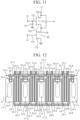
- FIG. 11 is an equivalent circuit diagram illustrating the high-frequency amplifier 1 according to the second embodiment.
- the same reference numerals as those in FIG. 4 denote the same or corresponding parts, and thus description thereof is omitted.
- the shunt feedback capacitor 51 is any one of the shunt feedback capacitors 51-1 to 51-4.
- the other end of the shunt feedback capacitor 51-j is connected to the drain finger 15-j.
- One end of the air bridge 52-j is connected to the drain finger 34-j, and the other end of the air bridge 52-j is connected to one end of the shunt feedback capacitor 51-j.
- the high-frequency amplifier 1 includes the shunt feedback capacitors 51-1 to 51-4, impedance matching between the common-source transistor 12 and the common-gate transistor 32 can be implemented.
- the shunt feedback capacitors 51-1 to 51-4 are arranged in a distributed manner for each of the drain fingers 15-j, an imbalanced operation of the drain fingers 15-1 to 15-4 is suppressed.
- the common-source transistor 12 and the common-gate transistor 32 are separate transistors. However, this is only an example, and for example, as illustrated in FIG. 12 , it is possible to use a dual gate transistor in which the common-source transistor 12 and the common-gate transistor 32 are implemented in one transistor cell.
- FIG. 12 is a configuration diagram illustrating another high-frequency amplifier 1 according to the second embodiment.
- the gate fingers 14-1 to 14-8, the source fingers 16-1 to 16-5, the drain source fingers 20-1 to 20-8, the drain fingers 34-1 to 34-4, and the gate fingers 35-1 to 35-8 are arranged in parallel with each other.
- the high-frequency amplifier 1 illustrated in FIG. 12 includes the capacitors 39-1, 39-8, 39-11, 39-12, and 39-13 similarly to the high-frequency amplifier 1 illustrated in FIG. 6 , but may include the capacitors 39-1 to 39-8 similarly to the high-frequency amplifier 1 illustrated in FIG. 3 .
- the common-source transistor 12 and the common-gate transistor 32 are implemented as a dual gate transistor, a high-frequency amplifier having a higher frequency or a wider band than the high-frequency amplifiers 1 illustrated in FIG. 10 can be implemented.
- the capacitors 39-1 to 39-8 or the capacitors 39-1, 39-8, 39-11, 39-12, and 39-13 are implemented by metal insulator metal (MIM) capacitors.
- MIM metal insulator metal
- the capacitors 39-1 to 39-8 and 39-11 to 39-13 are not limited to MIM capacitors, and may be implemented by, for example, interdigital capacitors.
- each of the capacitors 39-1 to 39-8 and the like is formed on any of the source fingers 16-1 to 16-5.
- this is only an example, and it is only required that each of the capacitors 39-1 to 39-8 and the like is disposed between each of the gate fingers 35-1 to 35-8 and each of the source fingers 16-1 to 16-5.
- Each of the capacitors 39-1 to 39-8 and the like may be formed on the gate bus bar 38 and then connected to the ground via an air bridge.
- each of the common-source transistor 12 and the common-gate transistor 32 is implemented by a GaN multi-finger transistor.
- each of the common-source transistor 12 and the common-gate transistor 32 may be a transistor formed on a substrate whose material is GaAs (gallium arsenide) or the like.
- each of the common-source transistor 12 and the common-gate transistor 32 may be implemented by a bipolar transistor instead of a field effect transistor.
- each capacitor 39 is disposed at a position sandwiched between two gate fingers 14 or a position adjacent to one gate finger 14.
- the capacitors 39-1 to 39-8 and the like are only required to be arranged at positions where the impedances obtained by looking toward the capacitor 39 from the respective gate fingers 35-m are equal to each other, and are not limited to those arranged as illustrated in FIG. 3 or 5 .
- the capacitors 39 may be dispersedly arranged in every several gate fingers 14, and the effect of reducing the imbalance is obtained.
- the common-source transistor 12 and the common-gate transistor 32 are cascade-connected as two transistors. However, this is only an example, and three or more transistors may be cascade-connected.
- the present disclosure is suitable for a high-frequency amplifier that amplifies a high-frequency signal.
- the present disclosure is suitable for a radio communication device including the high-frequency amplifier.
- the present disclosure is suitable for a radar device including the high-frequency amplifier.
Landscapes
- Engineering & Computer Science (AREA)
- Power Engineering (AREA)
- Microelectronics & Electronic Packaging (AREA)
- Amplifiers (AREA)
- Junction Field-Effect Transistors (AREA)
- Metal-Oxide And Bipolar Metal-Oxide Semiconductor Integrated Circuits (AREA)
Applications Claiming Priority (1)
| Application Number | Priority Date | Filing Date | Title |
|---|---|---|---|
| PCT/JP2020/015343 WO2021199431A1 (ja) | 2020-04-03 | 2020-04-03 | 高周波増幅器、無線通信装置及びレーダ装置 |
Publications (3)
| Publication Number | Publication Date |
|---|---|
| EP4113832A1 EP4113832A1 (en) | 2023-01-04 |
| EP4113832A4 EP4113832A4 (en) | 2023-08-02 |
| EP4113832B1 true EP4113832B1 (en) | 2025-04-23 |
Family
ID=77927770
Family Applications (1)
| Application Number | Title | Priority Date | Filing Date |
|---|---|---|---|
| EP20928877.8A Active EP4113832B1 (en) | 2020-04-03 | 2020-04-03 | High-frequency amplifier, radio communication device, and radar device |
Country Status (4)
| Country | Link |
|---|---|
| US (1) | US12456954B2 (https=) |
| EP (1) | EP4113832B1 (https=) |
| JP (1) | JP7195480B2 (https=) |
| WO (1) | WO2021199431A1 (https=) |
Families Citing this family (3)
| Publication number | Priority date | Publication date | Assignee | Title |
|---|---|---|---|---|
| JP2023049404A (ja) * | 2021-09-29 | 2023-04-10 | 住友電工デバイス・イノベーション株式会社 | 半導体装置 |
| EP4343831A1 (en) * | 2022-09-25 | 2024-03-27 | Wolfspeed, Inc. | Field effect transistor with integrated series capacitance |
| US12599008B2 (en) * | 2023-04-06 | 2026-04-07 | Nxp Usa, Inc. | Transistor with source manifold in non-active die region |
Family Cites Families (5)
| Publication number | Priority date | Publication date | Assignee | Title |
|---|---|---|---|---|
| JP3925417B2 (ja) | 2003-01-29 | 2007-06-06 | 富士通株式会社 | 分布型増幅器実装装置 |
| JP4821214B2 (ja) * | 2005-08-26 | 2011-11-24 | 三菱電機株式会社 | カスコード接続回路 |
| KR101726109B1 (ko) * | 2012-11-09 | 2017-04-11 | 미쓰비시덴키 가부시키가이샤 | 캐스코드 앰프 |
| JP6272102B2 (ja) * | 2014-03-27 | 2018-01-31 | 三菱電機株式会社 | カスコード増幅器 |
| JP7302925B2 (ja) * | 2018-08-29 | 2023-07-04 | 住友電工デバイス・イノベーション株式会社 | 高周波増幅器 |
-
2020
- 2020-04-03 WO PCT/JP2020/015343 patent/WO2021199431A1/ja not_active Ceased
- 2020-04-03 JP JP2022511484A patent/JP7195480B2/ja active Active
- 2020-04-03 EP EP20928877.8A patent/EP4113832B1/en active Active
-
2022
- 2022-08-05 US US17/882,105 patent/US12456954B2/en active Active
Also Published As
| Publication number | Publication date |
|---|---|
| JPWO2021199431A1 (https=) | 2021-10-07 |
| EP4113832A4 (en) | 2023-08-02 |
| US20220385246A1 (en) | 2022-12-01 |
| EP4113832A1 (en) | 2023-01-04 |
| US12456954B2 (en) | 2025-10-28 |
| JP7195480B2 (ja) | 2022-12-23 |
| WO2021199431A1 (ja) | 2021-10-07 |
Similar Documents
| Publication | Publication Date | Title |
|---|---|---|
| CN108462477B (zh) | 功率放大电路 | |
| US7804361B2 (en) | Low noise amplifier | |
| US9543914B2 (en) | Doherty amplifier structure | |
| US12456954B2 (en) | High-frequency amplifier, radio communication device, and radar device | |
| EP3700087A1 (en) | Doherty amplifier and doherty amplifier circuit | |
| US8437723B2 (en) | Amplifier circuit and communication device | |
| US7187231B2 (en) | Apparatus, methods and articles of manufacture for multiband signal processing | |
| US10511267B2 (en) | Power amplifier | |
| EP3337035A1 (en) | Inter-stage network for radio frequency amplifier | |
| Kingsley et al. | Adaptive amplifier module technique to support cognitive RF architectures | |
| US7750740B2 (en) | Semiconductor circuit | |
| US20250274082A1 (en) | Power amplifier circuit | |
| US7227392B2 (en) | Frequency multiplier | |
| US9647615B2 (en) | Broadband amplifier | |
| EP3771096B1 (en) | Amplifier | |
| US8570117B2 (en) | Bias circuit | |
| CN115242195A (zh) | 放大装置以及发送机 | |
| US12355401B2 (en) | Doherty amplifier | |
| US11387786B2 (en) | Amplifier | |
| US12176857B2 (en) | Doherty amplifier and communication device | |
| US20160285421A1 (en) | Power amplifier | |
| JP2006093857A (ja) | 歪補償回路 | |
| EP2579458A1 (en) | Switching circuit and envelope signal amplifier | |
| US20250343514A1 (en) | Amplification circuit and communication device | |
| US12580531B2 (en) | Radio frequency circuit and communication device |
Legal Events
| Date | Code | Title | Description |
|---|---|---|---|
| STAA | Information on the status of an ep patent application or granted ep patent |
Free format text: STATUS: THE INTERNATIONAL PUBLICATION HAS BEEN MADE |
|
| PUAI | Public reference made under article 153(3) epc to a published international application that has entered the european phase |
Free format text: ORIGINAL CODE: 0009012 |
|
| STAA | Information on the status of an ep patent application or granted ep patent |
Free format text: STATUS: REQUEST FOR EXAMINATION WAS MADE |
|
| 17P | Request for examination filed |
Effective date: 20220923 |
|
| AK | Designated contracting states |
Kind code of ref document: A1 Designated state(s): AL AT BE BG CH CY CZ DE DK EE ES FI FR GB GR HR HU IE IS IT LI LT LU LV MC MK MT NL NO PL PT RO RS SE SI SK SM TR |
|
| REG | Reference to a national code |
Ref country code: DE Ref legal event code: R079 Free format text: PREVIOUS MAIN CLASS: H03F0001220000 Ipc: H01L0023482000 Ref document number: 602020050199 Country of ref document: DE |
|
| DAV | Request for validation of the european patent (deleted) | ||
| DAX | Request for extension of the european patent (deleted) | ||
| A4 | Supplementary search report drawn up and despatched |
Effective date: 20230705 |
|
| RIC1 | Information provided on ipc code assigned before grant |
Ipc: H01L 23/48 20060101ALN20230629BHEP Ipc: H03F 3/24 20060101ALI20230629BHEP Ipc: H03F 3/195 20060101ALI20230629BHEP Ipc: H01L 27/06 20060101ALI20230629BHEP Ipc: H01L 27/02 20060101ALI20230629BHEP Ipc: H01L 23/66 20060101ALI20230629BHEP Ipc: H01L 23/522 20060101ALI20230629BHEP Ipc: H03F 3/193 20060101ALI20230629BHEP Ipc: H03F 1/22 20060101ALI20230629BHEP Ipc: H01L 23/482 20060101AFI20230629BHEP |
|
| STAA | Information on the status of an ep patent application or granted ep patent |
Free format text: STATUS: EXAMINATION IS IN PROGRESS |
|
| 17Q | First examination report despatched |
Effective date: 20240408 |
|
| GRAP | Despatch of communication of intention to grant a patent |
Free format text: ORIGINAL CODE: EPIDOSNIGR1 |
|
| STAA | Information on the status of an ep patent application or granted ep patent |
Free format text: STATUS: GRANT OF PATENT IS INTENDED |
|
| INTG | Intention to grant announced |
Effective date: 20241105 |
|
| GRAS | Grant fee paid |
Free format text: ORIGINAL CODE: EPIDOSNIGR3 |
|
| GRAA | (expected) grant |
Free format text: ORIGINAL CODE: 0009210 |
|
| STAA | Information on the status of an ep patent application or granted ep patent |
Free format text: STATUS: THE PATENT HAS BEEN GRANTED |
|
| AK | Designated contracting states |
Kind code of ref document: B1 Designated state(s): AL AT BE BG CH CY CZ DE DK EE ES FI FR GB GR HR HU IE IS IT LI LT LU LV MC MK MT NL NO PL PT RO RS SE SI SK SM TR |
|
| REG | Reference to a national code |
Ref country code: GB Ref legal event code: FG4D |
|
| REG | Reference to a national code |
Ref country code: CH Ref legal event code: EP |
|
| REG | Reference to a national code |
Ref country code: DE Ref legal event code: R096 Ref document number: 602020050199 Country of ref document: DE |
|
| REG | Reference to a national code |
Ref country code: IE Ref legal event code: FG4D |
|
| REG | Reference to a national code |
Ref country code: NL Ref legal event code: MP Effective date: 20250423 |
|
| PG25 | Lapsed in a contracting state [announced via postgrant information from national office to epo] |
Ref country code: NL Free format text: LAPSE BECAUSE OF FAILURE TO SUBMIT A TRANSLATION OF THE DESCRIPTION OR TO PAY THE FEE WITHIN THE PRESCRIBED TIME-LIMIT Effective date: 20250423 |
|
| REG | Reference to a national code |
Ref country code: AT Ref legal event code: MK05 Ref document number: 1788671 Country of ref document: AT Kind code of ref document: T Effective date: 20250423 |
|
| PG25 | Lapsed in a contracting state [announced via postgrant information from national office to epo] |
Ref country code: FI Free format text: LAPSE BECAUSE OF FAILURE TO SUBMIT A TRANSLATION OF THE DESCRIPTION OR TO PAY THE FEE WITHIN THE PRESCRIBED TIME-LIMIT Effective date: 20250423 Ref country code: PT Free format text: LAPSE BECAUSE OF FAILURE TO SUBMIT A TRANSLATION OF THE DESCRIPTION OR TO PAY THE FEE WITHIN THE PRESCRIBED TIME-LIMIT Effective date: 20250825 Ref country code: ES Free format text: LAPSE BECAUSE OF FAILURE TO SUBMIT A TRANSLATION OF THE DESCRIPTION OR TO PAY THE FEE WITHIN THE PRESCRIBED TIME-LIMIT Effective date: 20250423 |
|
| REG | Reference to a national code |
Ref country code: LT Ref legal event code: MG9D |
|
| PG25 | Lapsed in a contracting state [announced via postgrant information from national office to epo] |
Ref country code: GR Free format text: LAPSE BECAUSE OF FAILURE TO SUBMIT A TRANSLATION OF THE DESCRIPTION OR TO PAY THE FEE WITHIN THE PRESCRIBED TIME-LIMIT Effective date: 20250724 Ref country code: NO Free format text: LAPSE BECAUSE OF FAILURE TO SUBMIT A TRANSLATION OF THE DESCRIPTION OR TO PAY THE FEE WITHIN THE PRESCRIBED TIME-LIMIT Effective date: 20250723 |
|
| PG25 | Lapsed in a contracting state [announced via postgrant information from national office to epo] |
Ref country code: PL Free format text: LAPSE BECAUSE OF FAILURE TO SUBMIT A TRANSLATION OF THE DESCRIPTION OR TO PAY THE FEE WITHIN THE PRESCRIBED TIME-LIMIT Effective date: 20250423 |
|
| PG25 | Lapsed in a contracting state [announced via postgrant information from national office to epo] |
Ref country code: BG Free format text: LAPSE BECAUSE OF FAILURE TO SUBMIT A TRANSLATION OF THE DESCRIPTION OR TO PAY THE FEE WITHIN THE PRESCRIBED TIME-LIMIT Effective date: 20250423 |
|
| PG25 | Lapsed in a contracting state [announced via postgrant information from national office to epo] |
Ref country code: HR Free format text: LAPSE BECAUSE OF FAILURE TO SUBMIT A TRANSLATION OF THE DESCRIPTION OR TO PAY THE FEE WITHIN THE PRESCRIBED TIME-LIMIT Effective date: 20250423 |
|
| PG25 | Lapsed in a contracting state [announced via postgrant information from national office to epo] |
Ref country code: AT Free format text: LAPSE BECAUSE OF FAILURE TO SUBMIT A TRANSLATION OF THE DESCRIPTION OR TO PAY THE FEE WITHIN THE PRESCRIBED TIME-LIMIT Effective date: 20250423 |
|
| PG25 | Lapsed in a contracting state [announced via postgrant information from national office to epo] |
Ref country code: RS Free format text: LAPSE BECAUSE OF FAILURE TO SUBMIT A TRANSLATION OF THE DESCRIPTION OR TO PAY THE FEE WITHIN THE PRESCRIBED TIME-LIMIT Effective date: 20250723 |
|
| PG25 | Lapsed in a contracting state [announced via postgrant information from national office to epo] |
Ref country code: IS Free format text: LAPSE BECAUSE OF FAILURE TO SUBMIT A TRANSLATION OF THE DESCRIPTION OR TO PAY THE FEE WITHIN THE PRESCRIBED TIME-LIMIT Effective date: 20250823 |
|
| PG25 | Lapsed in a contracting state [announced via postgrant information from national office to epo] |
Ref country code: LV Free format text: LAPSE BECAUSE OF FAILURE TO SUBMIT A TRANSLATION OF THE DESCRIPTION OR TO PAY THE FEE WITHIN THE PRESCRIBED TIME-LIMIT Effective date: 20250423 |
|
| REG | Reference to a national code |
Ref country code: DE Ref legal event code: R079 Ref document number: 602020050199 Country of ref document: DE Free format text: PREVIOUS MAIN CLASS: H01L0023482000 Ipc: H10W0072000000 |
|
| PG25 | Lapsed in a contracting state [announced via postgrant information from national office to epo] |
Ref country code: DK Free format text: LAPSE BECAUSE OF FAILURE TO SUBMIT A TRANSLATION OF THE DESCRIPTION OR TO PAY THE FEE WITHIN THE PRESCRIBED TIME-LIMIT Effective date: 20250423 Ref country code: SM Free format text: LAPSE BECAUSE OF FAILURE TO SUBMIT A TRANSLATION OF THE DESCRIPTION OR TO PAY THE FEE WITHIN THE PRESCRIBED TIME-LIMIT Effective date: 20250423 |
|
| PG25 | Lapsed in a contracting state [announced via postgrant information from national office to epo] |
Ref country code: CZ Free format text: LAPSE BECAUSE OF FAILURE TO SUBMIT A TRANSLATION OF THE DESCRIPTION OR TO PAY THE FEE WITHIN THE PRESCRIBED TIME-LIMIT Effective date: 20250423 |
|
| PG25 | Lapsed in a contracting state [announced via postgrant information from national office to epo] |
Ref country code: EE Free format text: LAPSE BECAUSE OF FAILURE TO SUBMIT A TRANSLATION OF THE DESCRIPTION OR TO PAY THE FEE WITHIN THE PRESCRIBED TIME-LIMIT Effective date: 20250423 |
|
| REG | Reference to a national code |
Ref country code: DE Ref legal event code: R097 Ref document number: 602020050199 Country of ref document: DE |
|
| PG25 | Lapsed in a contracting state [announced via postgrant information from national office to epo] |
Ref country code: SK Free format text: LAPSE BECAUSE OF FAILURE TO SUBMIT A TRANSLATION OF THE DESCRIPTION OR TO PAY THE FEE WITHIN THE PRESCRIBED TIME-LIMIT Effective date: 20250423 |
|
| PG25 | Lapsed in a contracting state [announced via postgrant information from national office to epo] |
Ref country code: IT Free format text: LAPSE BECAUSE OF FAILURE TO SUBMIT A TRANSLATION OF THE DESCRIPTION OR TO PAY THE FEE WITHIN THE PRESCRIBED TIME-LIMIT Effective date: 20250423 |
|
| PLBE | No opposition filed within time limit |
Free format text: ORIGINAL CODE: 0009261 |
|
| STAA | Information on the status of an ep patent application or granted ep patent |
Free format text: STATUS: NO OPPOSITION FILED WITHIN TIME LIMIT |
|
| REG | Reference to a national code |
Ref country code: CH Ref legal event code: L10 Free format text: ST27 STATUS EVENT CODE: U-0-0-L10-L00 (AS PROVIDED BY THE NATIONAL OFFICE) Effective date: 20260304 |
|
| 26N | No opposition filed |
Effective date: 20260126 |
|
| PGFP | Annual fee paid to national office [announced via postgrant information from national office to epo] |
Ref country code: GB Payment date: 20260313 Year of fee payment: 7 |
|
| PGFP | Annual fee paid to national office [announced via postgrant information from national office to epo] |
Ref country code: FR Payment date: 20260309 Year of fee payment: 7 |