EP4113648B1 - Electrode-forming device equipped with notching pilot pin, and method for forming electrode using same - Google Patents
Electrode-forming device equipped with notching pilot pin, and method for forming electrode using same Download PDFInfo
- Publication number
- EP4113648B1 EP4113648B1 EP21880612.3A EP21880612A EP4113648B1 EP 4113648 B1 EP4113648 B1 EP 4113648B1 EP 21880612 A EP21880612 A EP 21880612A EP 4113648 B1 EP4113648 B1 EP 4113648B1
- Authority
- EP
- European Patent Office
- Prior art keywords
- electrode
- electrode sheet
- notching
- punching
- unit
- Prior art date
- Legal status (The legal status is an assumption and is not a legal conclusion. Google has not performed a legal analysis and makes no representation as to the accuracy of the status listed.)
- Active
Links
Images


Classifications
-
- H—ELECTRICITY
- H01—ELECTRIC ELEMENTS
- H01M—PROCESSES OR MEANS, e.g. BATTERIES, FOR THE DIRECT CONVERSION OF CHEMICAL ENERGY INTO ELECTRICAL ENERGY
- H01M4/00—Electrodes
- H01M4/02—Electrodes composed of, or comprising, active material
- H01M4/04—Processes of manufacture in general
-
- H—ELECTRICITY
- H01—ELECTRIC ELEMENTS
- H01M—PROCESSES OR MEANS, e.g. BATTERIES, FOR THE DIRECT CONVERSION OF CHEMICAL ENERGY INTO ELECTRICAL ENERGY
- H01M4/00—Electrodes
- H01M4/02—Electrodes composed of, or comprising, active material
- H01M4/04—Processes of manufacture in general
- H01M4/043—Processes of manufacture in general involving compressing or compaction
-
- B—PERFORMING OPERATIONS; TRANSPORTING
- B26—HAND CUTTING TOOLS; CUTTING; SEVERING
- B26F—PERFORATING; PUNCHING; CUTTING-OUT; STAMPING-OUT; SEVERING BY MEANS OTHER THAN CUTTING
- B26F1/00—Perforating; Punching; Cutting-out; Stamping-out; Apparatus therefor
- B26F1/02—Perforating by punching, e.g. with relatively-reciprocating punch and bed
- B26F1/12—Perforating by punching, e.g. with relatively-reciprocating punch and bed to notch margins of work
-
- B—PERFORMING OPERATIONS; TRANSPORTING
- B26—HAND CUTTING TOOLS; CUTTING; SEVERING
- B26F—PERFORATING; PUNCHING; CUTTING-OUT; STAMPING-OUT; SEVERING BY MEANS OTHER THAN CUTTING
- B26F1/00—Perforating; Punching; Cutting-out; Stamping-out; Apparatus therefor
- B26F1/02—Perforating by punching, e.g. with relatively-reciprocating punch and bed
- B26F1/14—Punching tools; Punching dies
-
- H—ELECTRICITY
- H01—ELECTRIC ELEMENTS
- H01M—PROCESSES OR MEANS, e.g. BATTERIES, FOR THE DIRECT CONVERSION OF CHEMICAL ENERGY INTO ELECTRICAL ENERGY
- H01M10/00—Secondary cells; Manufacture thereof
- H01M10/04—Construction or manufacture in general
- H01M10/0404—Machines for assembling batteries
-
- H—ELECTRICITY
- H01—ELECTRIC ELEMENTS
- H01M—PROCESSES OR MEANS, e.g. BATTERIES, FOR THE DIRECT CONVERSION OF CHEMICAL ENERGY INTO ELECTRICAL ENERGY
- H01M4/00—Electrodes
- H01M4/02—Electrodes composed of, or comprising, active material
- H01M4/04—Processes of manufacture in general
- H01M4/0402—Methods of deposition of the material
-
- H—ELECTRICITY
- H01—ELECTRIC ELEMENTS
- H01M—PROCESSES OR MEANS, e.g. BATTERIES, FOR THE DIRECT CONVERSION OF CHEMICAL ENERGY INTO ELECTRICAL ENERGY
- H01M50/00—Constructional details or processes of manufacture of the non-active parts of electrochemical cells other than fuel cells, e.g. hybrid cells
- H01M50/50—Current conducting connections for cells or batteries
- H01M50/531—Electrode connections inside a battery casing
- H01M50/54—Connection of several leads or tabs of plate-like electrode stacks, e.g. electrode pole straps or bridges
-
- B—PERFORMING OPERATIONS; TRANSPORTING
- B26—HAND CUTTING TOOLS; CUTTING; SEVERING
- B26F—PERFORATING; PUNCHING; CUTTING-OUT; STAMPING-OUT; SEVERING BY MEANS OTHER THAN CUTTING
- B26F2210/00—Perforating, punching, cutting-out, stamping-out, severing by means other than cutting of specific products
-
- Y—GENERAL TAGGING OF NEW TECHNOLOGICAL DEVELOPMENTS; GENERAL TAGGING OF CROSS-SECTIONAL TECHNOLOGIES SPANNING OVER SEVERAL SECTIONS OF THE IPC; TECHNICAL SUBJECTS COVERED BY FORMER USPC CROSS-REFERENCE ART COLLECTIONS [XRACs] AND DIGESTS
- Y02—TECHNOLOGIES OR APPLICATIONS FOR MITIGATION OR ADAPTATION AGAINST CLIMATE CHANGE
- Y02E—REDUCTION OF GREENHOUSE GAS [GHG] EMISSIONS, RELATED TO ENERGY GENERATION, TRANSMISSION OR DISTRIBUTION
- Y02E60/00—Enabling technologies; Technologies with a potential or indirect contribution to GHG emissions mitigation
- Y02E60/10—Energy storage using batteries
-
- Y—GENERAL TAGGING OF NEW TECHNOLOGICAL DEVELOPMENTS; GENERAL TAGGING OF CROSS-SECTIONAL TECHNOLOGIES SPANNING OVER SEVERAL SECTIONS OF THE IPC; TECHNICAL SUBJECTS COVERED BY FORMER USPC CROSS-REFERENCE ART COLLECTIONS [XRACs] AND DIGESTS
- Y02—TECHNOLOGIES OR APPLICATIONS FOR MITIGATION OR ADAPTATION AGAINST CLIMATE CHANGE
- Y02P—CLIMATE CHANGE MITIGATION TECHNOLOGIES IN THE PRODUCTION OR PROCESSING OF GOODS
- Y02P70/00—Climate change mitigation technologies in the production process for final industrial or consumer products
- Y02P70/50—Manufacturing or production processes characterised by the final manufactured product
Definitions
- the present invention relates to an electrode shaping apparatus having a notching pilot pin and an electrode shaping method using the same. More particularly, the present invention relates to an electrode shaping apparatus having a notching pilot pin configured to reduce a step that may occur during notching of an electrode and an electrode shaping method using the same.
- a secondary battery is manufactured by mounting an electrode assembly in a cylindrical or prismatic case made of a metal material or a pouch case made of a laminate sheet including aluminum, injecting an electrolytic solution into the case, and hermetically sealing the case.
- the electrode assembly which has a structure in which a positive electrode and a negative electrode are stacked in the state in which a separator is interposed therebetween, is classified as a jelly-roll type electrode assembly, which is configured to have a structure in which a long sheet type positive electrode having an active material applied thereto and a long sheet type negative electrode having an active material applied thereto are wound in the state in which a separator is interposed therebetween; a stacked type electrode assembly which is configured to have a structure in which a flat positive electrode and a flat negative electrode are stacked in the state in which a separator is interposed therebetween; a stacked and folded type electrode assembly, which is configured to have a structure in which unit cells are wound in a state of being disposed on a long sheet type separator; or a laminated and stacked type electrode assembly, which is configured to have a structure in which unit cells are stacked in the state in which a separator is interposed therebetween.
- a single-sided electrode plate or a double-sided electrode plate configured such that an electrode active material is applied to one surface or opposite surfaces of a current collector is used.
- a method of manufacturing the electrode assembly includes a process of manufacturing an electrode sheet, a process of pressing the electrode sheet, a process of slitting the electrode sheet by a predetermined length so as to be suitable for the standards of a cell, a vacuum drying process, a process of notching an electrode tab on the electrode sheet, and a process of manufacturing an electrode assembly including the electrode sheet and a separator.
- FIG. 1 is a plan view showing a portion of a conventional electrode manufacturing process.
- an electrode material coating portion 120 is formed on only a portion of the electrode sheet 110 excluding opposite side outer peripheries 111 and a middle part of the electrode sheet in a transfer direction A, and an electrode material non-coating portion 121 is formed on the remaining portion of the electrode sheet excluding the electrode material coating portion 120.
- the electrode sheet 110 is divided into two equal parts, i.e., two unit electrode sheets 130, along a slitting line 112 at the middle part of the electrode sheet 110 in the transfer direction A.
- a first side outer periphery 114 of the unit electrode sheet 130 divided along the slitting line 112 in the transfer direction A is notched in order to form an electrode tab 113
- a second side outer periphery 115 of the unit electrode sheet is notched in order to form a portion to be cut for manufacture of a unit electrode.
- the electrode tab 113 may be simultaneously notched when the electrode sheet is divided into two equal parts along the slitting line 112.
- notching includes not only a process of cutting the electrode tab so as to fit the shape thereof but also cutting the electrode sheet into two equal parts along the slitting line.
- the electrode sheet and a sheet include a metal electrode sheet with or without an electrode material coating portion.
- the electrode sheet When the electrode is notched, theoretically, the electrode sheet must be cut so as to be parallel to the transfer direction of the electrode sheet and the electrode tab must be cut so as to be perpendicular thereto, as shown in the upper part of FIG. 2 .
- the electrode material coating portion 120 and the electrode material non-coating portion 121 are different in thickness from each other.
- the electrode tab When notching is performed, therefore, the electrode tab is not correctly cut but is cut (notched) in a retarded state, i.e., meandering defects occur (see the lower part of FIG. 2 ).
- Patent Document 1 discloses a method of manufacturing an electrode plate for batteries that continuously forms a plurality of electrode plates from a belt type or hoop type electrode plate by punching using a punching press constituted by an upper press and a lower press capable of moving upwards and downwards, wherein the upper press has a punch and a shear blade mounted in the front thereof in a cutting direction, the lower press has a die having a punch hole, into which the punch is inserted, and a shear blade mounted in the front thereof in the cutting direction, when punching is performed in the state in which opposite sides of electrode plates are adjacent to each other as a common side in a longitudinal direction of the electrode plate, on the assumption that one of the opposite sides in a direction in which the electrode plates are adjacent to each other is opposite side A and the common side is side B, a corner formed by side A and side B is chamfered, and the lower press is configured such that a stepped upper part having two or more steps having a hole size increased stepwise in the punching direction is formed in the lower part of
- Patent Document 1 does not disclose the construction of the notching pilot pin according to the present invention, and does not suggest a solution to the problem to be solved by the present invention, since this document relates to preventing clogging due to cut scraps of the electrode plate and increasing the lifespan of the notching punch.
- Patent Document 2 discloses a notching apparatus for notching a continuous electrode sheet having an electrode active material applied to one surface or opposite surfaces thereof at unit electrode intervals in order to manufacture a plurality of unit electrodes from the electrode sheet, the notching apparatus including a press configured to notch the upper end and the lower end of the electrode sheet in the state in which the position of the press is fixed and two or more grippers located at the rear of the press in a direction in which the electrode sheet is supplied, the grippers being configured to hold and transfer the electrode sheet by one pitch, which is a size corresponding to a unit electrode, in response to the operation of the press, wherein, when one of the grippers holds and transfers the electrode sheet, the other grippers moves to positions for holding.
- Patent Document 2 is characterized in that notches are formed in the electrode sheet, and the electrode sheet is supplied by one pitch by the first and second grippers and is then punched, whereby notching is performed at predetermined intervals, which, however, is not a solution to meandering defects.
- Patent Document 3 discloses an electrode manufacturing apparatus including a notching roller, the electrode manufacturing apparatus including a transfer unit configured to continuously transfer a first electrode sheet having an electrode active material applied to a long sheet type current collector in order to notch and cut the first electrode sheet, a notching roller having a cylindrical structure, the notching roller being configured to notch one surface of the first electrode sheet by rotation in order to manufacture a second electrode sheet having one side outer periphery and the other side outer periphery continuously formed, and a cutter configured to cut the notched second electrode sheet to a length corresponding to the width of the electrode in order to manufacture a final electrode, wherein the notching roller includes a first notching portion configured to form one side outer periphery of the second electrode sheet and a second notching portion configured to form the other side outer periphery of the second electrode sheet when viewed in plan.
- Patent Document 3 it is described that the notching roller is used, whereby no notching step occurs.
- the roller type roller deviation in thickness between an electrode material coating portion and an electrode material non-coating portion is continuously accumulated, whereby meandering defects may be increased, and Patent Document 3 does not recognize such a problem.
- Patent Document 4 relates to a press apparatus configured to form a plurality of electrode plates of a lithium ion polymer battery used in a hybrid electric vehicle at once, wherein an upper press having a cutting means and a lower press configured to assist the upper press are installed, a thin flat electrode plate material is continuously supplied therebetween to simultaneously form a plurality of electrode plate members provided in a battery, whereby it is possible to accurately, uniformly, and continuously manufacture a plurality of electrode plates at once.
- Patent Document 4 a notching portion is formed on a middle cutter blade such that punching is performed while the boundary between the electrode plate members is marked; A punching unit is configured to remove a portion of an outer periphery of the electrode sheet by notching. however, this document does not recognize a problem of meandering defects.
- the present invention has been made in view of the above problems, and it is an object of the present invention to provide an electrode shaping apparatus capable of solving a problem of a step being formed at an electrode tab that may occur during notching and an electrode shaping method using the same.
- the present invention provides an electrode shaping apparatus including a sheet transfer unit configured to move an electrode sheet at a predetermined speed; a fixing unit configured to fix the electrode sheet; and a punch unit including a center punching unit configured to remove a central part of the electrode sheet and a side punching unit configured to remove a portion of an outer periphery of the electrode sheet by notching, wherein the center punching unit includes a hole punching member and a notching pilot pin.
- the center punching unit includes a rectangular parallelepiped main body having a major axis in a movement direction of the electrode sheet; the hole punching member formed at a rear end of the main body in the movement direction of the electrode sheet; and the notching pilot pin formed under a front end of the main body in the movement direction of the electrode sheet.
- a pin punching portion is configured to punch a catching recess, in which the notching pilot pin is configured to be caught.
- the main body may be formed in a rectangular parallelepiped shape having a major axis in the movement direction of the electrode sheet, and may include a main body punching surface configured to punch the electrode sheet as the lower surface of the rectangular parallelepiped.
- the hole punching member may include an enlarged portion extending from the rear end of the main body in the movement direction of the electrode sheet, the width of the punching surface being increased at the enlarged portion and configured to punch the electrode sheet; a reduced portion extending from the enlarged portion, the width of the punching surface being decreased at the reduced portion along the major axis and configured to punch the electrode sheet; and a pin punching portion extending from the reduced portion, the pin punching portion configured to punch a catching recess, in which the notching pilot pin is configured to be caught, in the electrode sheet.
- the section of the notching pilot pin may be any one of a circle, an arc, a wedge, a triangle, and a quadrangle.
- the fixing unit may be provided in the middle thereof with a middle groove corresponding in shape to the center punching unit.
- the middle groove may have a sufficient depth for the notching pilot pin to be inserted into the middle groove.
- the present invention provides an electrode shaping method using the electrode shaping apparatus, the electrode shaping method including S1) transferring an electrode sheet by a predetermined length using the sheet transfer unit; S2) transferring the electrode sheet or the punch unit such that the notching pilot pin is caught in a recess formed in the electrode sheet in a previous step of punching such that the notching pilot pin is caught in the recess; S3) pressing the electrode sheet using the punch unit to punch the electrode sheet; and S4) spacing the punch unit apart from the electrode sheet.
- a distance by which the punch unit is spaced apart from the electrode sheet may be equal to or less than a distance by which at least a portion of the notching pilot pin remains inserted in the recess of the electrode sheet.
- an electrode shaping apparatus having a notching pilot pin according to the present invention and an electrode shaping method using the same have an effect in that it is possible to solve a problem, which may occur during notching, of a step being formed at an electrode tab, compared to a conventional electrode shaping apparatus.
- the present invention has an effect in that it is possible to remove meandering defects that may occur in the conventional electrode shaping apparatus, whereby 1) an upper layer and a lower layer are accurately aligned with each other in a stacking process to manufacture the electrode assembly, whereby efficiency of a battery is increased, 2) there is no protruding portion of the electrode tab, whereby damage to a separator and occurrence of a short circuit are prevented, and 3) when each electrode is rotated during manufacture of the electrode assembly, a criterion based on which the position of the electrodes is accurately controlled and the electrodes are stacked becomes clear.
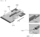
- FIG. 3 is a perspective view of an electrode shaping apparatus according to an embodiment of the present invention
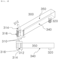
- FIG. 4 is a perspective view and a sectional view of a center punching unit according to an embodiment of the present invention
- FIG. 5 is a schematic view showing a coupling relationship between a notching pilot pin and a catching recess according to an embodiment of the present invention.
- the electrode shaping apparatus includes a sheet transfer unit (not shown) configured to move an electrode sheet 110 at a predetermined speed; a fixing unit 200 configured to fix the electrode sheet 110; and a punch unit constituted by a center punching unit 300 and a side punching unit (not shown) configured respectively to remove a central part of the electrode sheet and a portion of the outer periphery of the electrode sheet by notching, wherein the center punching unit 300 includes a hole punching member 310 and a notching pilot pin 320.
- the side punching unit is configured to perform notching into a special shape, as shown in FIG. 3 , or to perform notching into a common electrode tab shape, as shown in FIG. 2 .
- the present invention is not limited thereto.
- the center punching unit 300 includes a rectangular parallelepiped main body 350 having a major axis in a movement direction A of the electrode sheet 110, the hole punching member 310 formed at the rear end of the main body 350 in the movement direction A of the electrode sheet 110, and the notching pilot pin 320 formed under the front end of the main body 350 in the movement direction A of the electrode sheet 110.
- the main body 350 may be formed in a rectangular parallelepiped shape having a major axis in the movement direction A of the electrode sheet 110, and may include a main body punching surface 340 configured to punch the electrode sheet as the lower surface of the rectangular parallelepiped.
- the hole punching member 310 may include an enlarged portion 312 extending from the rear end of the main body 350 in the movement direction A of the electrode sheet 110, the width of the punching surface configured to punch the electrode sheet being increased at the enlarged portion; a reduced portion 314 extending from the enlarged portion 312, the width of the punching surface configured to punch the electrode sheet 110 being decreased at the reduced portion along the major axis A; and a pin punching portion 316 extending from the reduced portion 314, the pin punching portion 316 being configured to punch a catching recess 116, in which the notching pilot pin 320 is caught, in the electrode sheet 110.
- the catching recess 116 is formed in the electrode sheet 110 as indicated by a dotted line in FIG. 5 , and is formed in the electrode sheet 110 as indicated by a blue color in FIG. 3 .
- the section of the notching pilot pin 320 may be any one of a circle, an arc, a wedge, a triangle, and a quadrangle, although the notching pilot pin is formed in a cylindrical shape as shown in FIGS. 3 to 5 .
- the wedge type or triangular notching pilot pin may be connected to the reduced portion 314 in order not only to perform alignment in the transfer direction A of the electrode sheet 110 but also to perform alignment in a direction perpendicular to the transfer direction A.
- the fixing unit 200 may be provided in the middle thereof with a middle groove 210 corresponding in shape to the center punching unit.
- the middle groove 210 may be formed so as to have a sufficient depth for the notching pilot pin 320 to be inserted thereinto.
- the present invention provides an electrode shaping method using the electrode shaping apparatus, the electrode shaping method including S1) a step of transferring an electrode sheet by a predetermined length using the sheet transfer unit; S2) a step of transferring the electrode sheet or the punch unit such that the notching pilot pin is caught in a recess formed in the electrode sheet in a previous step of punching such that the notching pilot pin is caught in the recess; S3) a step of pressing the electrode sheet using the punch unit to punch the electrode sheet; and S4) a step of spacing the punch unit apart from the electrode sheet.
- step S4) the distance by which the punch unit is spaced apart from the electrode sheet is equal to or less than the distance by which at least a portion of the notching pilot pin remains inserted in the recess of the electrode sheet.
- the electrode shaping apparatus having the notching pilot pin according to the present invention and the electrode shaping method using the same have an effect in that it is possible to solve a problem of a step being formed at an electrode tab that may occur during notching, compared to a conventional electrode shaping apparatus.
- the present invention relates to an electrode shaping apparatus having a notching pilot pin configured to reduce a step that may occur during notching of an electrode and an electrode shaping method using the same, and therefore the present invention has industrial applicability.
Landscapes
- Engineering & Computer Science (AREA)
- Chemical & Material Sciences (AREA)
- Chemical Kinetics & Catalysis (AREA)
- Electrochemistry (AREA)
- General Chemical & Material Sciences (AREA)
- Manufacturing & Machinery (AREA)
- Life Sciences & Earth Sciences (AREA)
- Forests & Forestry (AREA)
- Mechanical Engineering (AREA)
- Battery Electrode And Active Subsutance (AREA)
Applications Claiming Priority (2)
| Application Number | Priority Date | Filing Date | Title |
|---|---|---|---|
| KR1020200134693A KR102820000B1 (ko) | 2020-10-16 | 2020-10-16 | 노칭 파일럿 핀을 구비한 전극 성형 장치 및 이를 이용하여 전극을 성형하는 방법 |
| PCT/KR2021/014395 WO2022080966A1 (ko) | 2020-10-16 | 2021-10-15 | 노칭 파일럿 핀을 구비한 전극 성형 장치 및 이를 이용하여 전극을 성형하는 방법 |
Publications (3)
| Publication Number | Publication Date |
|---|---|
| EP4113648A1 EP4113648A1 (en) | 2023-01-04 |
| EP4113648A4 EP4113648A4 (en) | 2023-10-25 |
| EP4113648B1 true EP4113648B1 (en) | 2025-01-29 |
Family
ID=81207396
Family Applications (1)
| Application Number | Title | Priority Date | Filing Date |
|---|---|---|---|
| EP21880612.3A Active EP4113648B1 (en) | 2020-10-16 | 2021-10-15 | Electrode-forming device equipped with notching pilot pin, and method for forming electrode using same |
Country Status (9)
| Country | Link |
|---|---|
| US (1) | US11901541B2 (pl) |
| EP (1) | EP4113648B1 (pl) |
| JP (1) | JP7477077B2 (pl) |
| KR (1) | KR102820000B1 (pl) |
| CN (1) | CN115380396B (pl) |
| ES (1) | ES3015187T3 (pl) |
| HU (1) | HUE070627T2 (pl) |
| PL (1) | PL4113648T3 (pl) |
| WO (1) | WO2022080966A1 (pl) |
Family Cites Families (13)
| Publication number | Priority date | Publication date | Assignee | Title |
|---|---|---|---|---|
| JP5159007B2 (ja) | 2001-05-11 | 2013-03-06 | パナソニック株式会社 | 電池用極板の製造方法 |
| KR100872498B1 (ko) | 2007-06-13 | 2008-12-05 | (주)한국대화금속 | 프레스 가공 장치 |
| JP2011081964A (ja) * | 2009-10-05 | 2011-04-21 | Toshiba Corp | 電極の製造装置、電極の製造方法、電極及び非水電解質電池 |
| KR101326628B1 (ko) | 2010-12-02 | 2013-11-07 | 주식회사 엘지화학 | 신규한 노칭 장치 및 이를 사용하여 생산되는 이차전지 |
| KR101313971B1 (ko) * | 2011-12-07 | 2013-10-01 | 세방전지(주) | 천공 스위치를 가지는 리튬 이차 전지 |
| KR101719026B1 (ko) * | 2013-08-30 | 2017-03-22 | 주식회사 엘지화학 | 전극판 제조 방법 및 이에 의해 제조되는 전극판 및 이차 전지 |
| EP3316349B1 (en) * | 2015-06-25 | 2022-02-23 | Envision AESC Japan Ltd. | Method for manufacturing electrochemical device |
| KR102026126B1 (ko) | 2015-10-27 | 2019-09-27 | 주식회사 엘지화학 | 노칭 롤러를 포함하고 있는 전극 제조 장치 |
| KR101737790B1 (ko) | 2016-07-15 | 2017-05-19 | 안혁 | 하이브리드 자동차용 전지 극판을 동시에 복수 개 가공하는 프레스 금형장치 |
| KR101901777B1 (ko) * | 2017-09-27 | 2018-09-28 | 주성용 | 단조에 의한 단자용 금속 부품 제조 방법 및 이에 의해 제조된 단자용 금속 부품 |
| KR102219013B1 (ko) * | 2019-03-22 | 2021-02-23 | 주식회사 엠플러스 | 노칭 금형의 엣지 포지션 컨트롤러 기능을 구현한 노칭 복합장비 |
| KR102757189B1 (ko) * | 2019-03-28 | 2025-01-21 | 주식회사 엘지에너지솔루션 | 이차전지용 전극 제조장치와, 이를 통해 제조된 이차전지용 전극 및 이차전지 |
| KR20200134693A (ko) | 2019-05-23 | 2020-12-02 | 주식회사 동진쎄미켐 | 신규 화합물 및 이를 포함하는 유기발광 소자 |
-
2020
- 2020-10-16 KR KR1020200134693A patent/KR102820000B1/ko active Active
-
2021
- 2021-10-15 US US18/013,114 patent/US11901541B2/en active Active
- 2021-10-15 ES ES21880612T patent/ES3015187T3/es active Active
- 2021-10-15 EP EP21880612.3A patent/EP4113648B1/en active Active
- 2021-10-15 WO PCT/KR2021/014395 patent/WO2022080966A1/ko not_active Ceased
- 2021-10-15 CN CN202180028119.8A patent/CN115380396B/zh active Active
- 2021-10-15 PL PL21880612.3T patent/PL4113648T3/pl unknown
- 2021-10-15 JP JP2022562486A patent/JP7477077B2/ja active Active
- 2021-10-15 HU HUE21880612A patent/HUE070627T2/hu unknown
Also Published As
| Publication number | Publication date |
|---|---|
| PL4113648T3 (pl) | 2025-04-14 |
| JP7477077B2 (ja) | 2024-05-01 |
| KR102820000B1 (ko) | 2025-06-12 |
| EP4113648A1 (en) | 2023-01-04 |
| US11901541B2 (en) | 2024-02-13 |
| ES3015187T3 (en) | 2025-04-30 |
| EP4113648A4 (en) | 2023-10-25 |
| HUE070627T2 (hu) | 2025-06-28 |
| KR20220050709A (ko) | 2022-04-25 |
| CN115380396A (zh) | 2022-11-22 |
| CN115380396B (zh) | 2025-05-16 |
| JP2023522648A (ja) | 2023-05-31 |
| US20230335702A1 (en) | 2023-10-19 |
| WO2022080966A1 (ko) | 2022-04-21 |
Similar Documents
| Publication | Publication Date | Title |
|---|---|---|
| JP7789806B2 (ja) | 電池用電極板、電池及び電池用電極板の製作方法 | |
| US20160111699A1 (en) | Electrode assembly block and method of manufacturing the same, and secondary battery and method of manufacturing the same | |
| EP2487738A1 (en) | Electrode assembly and secondary battery using the same | |
| US11050103B2 (en) | Pouch cell and method of forming same | |
| US10693192B2 (en) | Wound-type cell | |
| CN101507040A (zh) | 蓄电装置和制造蓄电装置的方法 | |
| KR101147241B1 (ko) | 전극 어셈블리, 이차 전지, 및 전극의 제조 방법 | |
| US12087900B2 (en) | Method of manufacturing electrode plate for battery, method of manufacturing battery, and battery | |
| CN111525178A (zh) | 二次电池 | |
| JP2023521720A (ja) | 電極の積層特性を改善した負極シート及び負極を含む電極組立体及びその製造方法 | |
| KR102403673B1 (ko) | 전극 조립체, 이를 포함하는 이차 전지 및 전극 조립체의 제조 방법 | |
| EP4113648B1 (en) | Electrode-forming device equipped with notching pilot pin, and method for forming electrode using same | |
| KR102196103B1 (ko) | 전극조립체의 제조방법 및 이에 의해서 제조된 전극조립체 및 이를 포함하는 리튬이차전지 | |
| CN116404269A (zh) | 电芯、电池及用电设备 | |
| KR102152213B1 (ko) | 전극조립체 제조방법 및 그를 포함하는 이차전지 제조방법 | |
| KR102914055B1 (ko) | 단위 셀 제조 장치 및 방법 | |
| KR20220021841A (ko) | 전극의 적층 특성을 개선한 음극시트 및 음극을 포함하는 전극조립체 및 그 제조방법 | |
| CN115939686A (zh) | 多极耳电芯制造方法及极片 | |
| KR102205425B1 (ko) | 이차전지용 전극 조립체, 이의 제조 방법 및 이를 포함하는 리튬이차전지 | |
| KR20210104264A (ko) | 전극 제조방법 및 이에 사용되는 전극 제조장치 | |
| US20250125361A1 (en) | Secondary battery and method for manufacturing secondary battery | |
| KR20180006732A (ko) | 이차전지 | |
| EP4550512A1 (en) | Method for manufacturing electrode assembly with improved processability, and electrode assembly manufactured using same | |
| KR102920239B1 (ko) | 전극조립체 제조 방법 | |
| EP4625512A1 (en) | Electrode for secondary battery and manufacturing method thereof |
Legal Events
| Date | Code | Title | Description |
|---|---|---|---|
| STAA | Information on the status of an ep patent application or granted ep patent |
Free format text: STATUS: THE INTERNATIONAL PUBLICATION HAS BEEN MADE |
|
| PUAI | Public reference made under article 153(3) epc to a published international application that has entered the european phase |
Free format text: ORIGINAL CODE: 0009012 |
|
| STAA | Information on the status of an ep patent application or granted ep patent |
Free format text: STATUS: REQUEST FOR EXAMINATION WAS MADE |
|
| 17P | Request for examination filed |
Effective date: 20220926 |
|
| AK | Designated contracting states |
Kind code of ref document: A1 Designated state(s): AL AT BE BG CH CY CZ DE DK EE ES FI FR GB GR HR HU IE IS IT LI LT LU LV MC MK MT NL NO PL PT RO RS SE SI SK SM TR |
|
| A4 | Supplementary search report drawn up and despatched |
Effective date: 20230925 |
|
| RIC1 | Information provided on ipc code assigned before grant |
Ipc: B26F 1/14 20060101ALI20230919BHEP Ipc: B26F 1/12 20060101ALI20230919BHEP Ipc: H01M 50/531 20210101ALI20230919BHEP Ipc: H01M 4/04 20060101AFI20230919BHEP |
|
| DAV | Request for validation of the european patent (deleted) | ||
| DAX | Request for extension of the european patent (deleted) | ||
| STAA | Information on the status of an ep patent application or granted ep patent |
Free format text: STATUS: EXAMINATION IS IN PROGRESS |
|
| 17Q | First examination report despatched |
Effective date: 20240411 |
|
| GRAP | Despatch of communication of intention to grant a patent |
Free format text: ORIGINAL CODE: EPIDOSNIGR1 |
|
| STAA | Information on the status of an ep patent application or granted ep patent |
Free format text: STATUS: GRANT OF PATENT IS INTENDED |
|
| INTG | Intention to grant announced |
Effective date: 20241014 |
|
| P01 | Opt-out of the competence of the unified patent court (upc) registered |
Free format text: CASE NUMBER: APP_59669/2024 Effective date: 20241104 |
|
| GRAS | Grant fee paid |
Free format text: ORIGINAL CODE: EPIDOSNIGR3 |
|
| GRAA | (expected) grant |
Free format text: ORIGINAL CODE: 0009210 |
|
| STAA | Information on the status of an ep patent application or granted ep patent |
Free format text: STATUS: THE PATENT HAS BEEN GRANTED |
|
| AK | Designated contracting states |
Kind code of ref document: B1 Designated state(s): AL AT BE BG CH CY CZ DE DK EE ES FI FR GB GR HR HU IE IS IT LI LT LU LV MC MK MT NL NO PL PT RO RS SE SI SK SM TR |
|
| REG | Reference to a national code |
Ref country code: GB Ref legal event code: FG4D |
|
| REG | Reference to a national code |
Ref country code: CH Ref legal event code: EP |
|
| REG | Reference to a national code |
Ref country code: DE Ref legal event code: R096 Ref document number: 602021025680 Country of ref document: DE |
|
| REG | Reference to a national code |
Ref country code: IE Ref legal event code: FG4D Ref country code: NL Ref legal event code: FP |
|
| REG | Reference to a national code |
Ref country code: SE Ref legal event code: TRGR |
|
| REG | Reference to a national code |
Ref country code: ES Ref legal event code: FG2A Ref document number: 3015187 Country of ref document: ES Kind code of ref document: T3 Effective date: 20250430 |
|
| REG | Reference to a national code |
Ref country code: HU Ref legal event code: AG4A Ref document number: E070627 Country of ref document: HU |
|
| PG25 | Lapsed in a contracting state [announced via postgrant information from national office to epo] |
Ref country code: RS Free format text: LAPSE BECAUSE OF FAILURE TO SUBMIT A TRANSLATION OF THE DESCRIPTION OR TO PAY THE FEE WITHIN THE PRESCRIBED TIME-LIMIT Effective date: 20250429 |
|
| PG25 | Lapsed in a contracting state [announced via postgrant information from national office to epo] |
Ref country code: FI Free format text: LAPSE BECAUSE OF FAILURE TO SUBMIT A TRANSLATION OF THE DESCRIPTION OR TO PAY THE FEE WITHIN THE PRESCRIBED TIME-LIMIT Effective date: 20250129 |
|
| REG | Reference to a national code |
Ref country code: LT Ref legal event code: MG9D |
|
| PG25 | Lapsed in a contracting state [announced via postgrant information from national office to epo] |
Ref country code: IS Free format text: LAPSE BECAUSE OF FAILURE TO SUBMIT A TRANSLATION OF THE DESCRIPTION OR TO PAY THE FEE WITHIN THE PRESCRIBED TIME-LIMIT Effective date: 20250529 Ref country code: NO Free format text: LAPSE BECAUSE OF FAILURE TO SUBMIT A TRANSLATION OF THE DESCRIPTION OR TO PAY THE FEE WITHIN THE PRESCRIBED TIME-LIMIT Effective date: 20250429 |
|
| REG | Reference to a national code |
Ref country code: AT Ref legal event code: MK05 Ref document number: 1764371 Country of ref document: AT Kind code of ref document: T Effective date: 20250129 |
|
| PG25 | Lapsed in a contracting state [announced via postgrant information from national office to epo] |
Ref country code: HR Free format text: LAPSE BECAUSE OF FAILURE TO SUBMIT A TRANSLATION OF THE DESCRIPTION OR TO PAY THE FEE WITHIN THE PRESCRIBED TIME-LIMIT Effective date: 20250129 |
|
| PG25 | Lapsed in a contracting state [announced via postgrant information from national office to epo] |
Ref country code: PT Free format text: LAPSE BECAUSE OF FAILURE TO SUBMIT A TRANSLATION OF THE DESCRIPTION OR TO PAY THE FEE WITHIN THE PRESCRIBED TIME-LIMIT Effective date: 20250529 Ref country code: LV Free format text: LAPSE BECAUSE OF FAILURE TO SUBMIT A TRANSLATION OF THE DESCRIPTION OR TO PAY THE FEE WITHIN THE PRESCRIBED TIME-LIMIT Effective date: 20250129 |
|
| PG25 | Lapsed in a contracting state [announced via postgrant information from national office to epo] |
Ref country code: GR Free format text: LAPSE BECAUSE OF FAILURE TO SUBMIT A TRANSLATION OF THE DESCRIPTION OR TO PAY THE FEE WITHIN THE PRESCRIBED TIME-LIMIT Effective date: 20250430 Ref country code: BG Free format text: LAPSE BECAUSE OF FAILURE TO SUBMIT A TRANSLATION OF THE DESCRIPTION OR TO PAY THE FEE WITHIN THE PRESCRIBED TIME-LIMIT Effective date: 20250129 |
|
| PG25 | Lapsed in a contracting state [announced via postgrant information from national office to epo] |
Ref country code: AT Free format text: LAPSE BECAUSE OF FAILURE TO SUBMIT A TRANSLATION OF THE DESCRIPTION OR TO PAY THE FEE WITHIN THE PRESCRIBED TIME-LIMIT Effective date: 20250129 |
|
| PG25 | Lapsed in a contracting state [announced via postgrant information from national office to epo] |
Ref country code: SM Free format text: LAPSE BECAUSE OF FAILURE TO SUBMIT A TRANSLATION OF THE DESCRIPTION OR TO PAY THE FEE WITHIN THE PRESCRIBED TIME-LIMIT Effective date: 20250129 |
|
| PG25 | Lapsed in a contracting state [announced via postgrant information from national office to epo] |
Ref country code: DK Free format text: LAPSE BECAUSE OF FAILURE TO SUBMIT A TRANSLATION OF THE DESCRIPTION OR TO PAY THE FEE WITHIN THE PRESCRIBED TIME-LIMIT Effective date: 20250129 |
|
| PGFP | Annual fee paid to national office [announced via postgrant information from national office to epo] |
Ref country code: TR Payment date: 20250924 Year of fee payment: 5 Ref country code: NL Payment date: 20250922 Year of fee payment: 5 Ref country code: IT Payment date: 20250924 Year of fee payment: 5 |
|
| PGFP | Annual fee paid to national office [announced via postgrant information from national office to epo] |
Ref country code: BE Payment date: 20250922 Year of fee payment: 5 Ref country code: GB Payment date: 20250922 Year of fee payment: 5 |
|
| PGFP | Annual fee paid to national office [announced via postgrant information from national office to epo] |
Ref country code: FR Payment date: 20250925 Year of fee payment: 5 |
|
| PGFP | Annual fee paid to national office [announced via postgrant information from national office to epo] |
Ref country code: SE Payment date: 20250923 Year of fee payment: 5 |
|
| PG25 | Lapsed in a contracting state [announced via postgrant information from national office to epo] |
Ref country code: EE Free format text: LAPSE BECAUSE OF FAILURE TO SUBMIT A TRANSLATION OF THE DESCRIPTION OR TO PAY THE FEE WITHIN THE PRESCRIBED TIME-LIMIT Effective date: 20250129 Ref country code: CZ Free format text: LAPSE BECAUSE OF FAILURE TO SUBMIT A TRANSLATION OF THE DESCRIPTION OR TO PAY THE FEE WITHIN THE PRESCRIBED TIME-LIMIT Effective date: 20250129 |
|
| PG25 | Lapsed in a contracting state [announced via postgrant information from national office to epo] |
Ref country code: RO Free format text: LAPSE BECAUSE OF FAILURE TO SUBMIT A TRANSLATION OF THE DESCRIPTION OR TO PAY THE FEE WITHIN THE PRESCRIBED TIME-LIMIT Effective date: 20250129 |
|
| PG25 | Lapsed in a contracting state [announced via postgrant information from national office to epo] |
Ref country code: SK Free format text: LAPSE BECAUSE OF FAILURE TO SUBMIT A TRANSLATION OF THE DESCRIPTION OR TO PAY THE FEE WITHIN THE PRESCRIBED TIME-LIMIT Effective date: 20250129 |
|
| REG | Reference to a national code |
Ref country code: DE Ref legal event code: R097 Ref document number: 602021025680 Country of ref document: DE |
|
| PGFP | Annual fee paid to national office [announced via postgrant information from national office to epo] |
Ref country code: HU Payment date: 20251029 Year of fee payment: 5 |
|
| PLBE | No opposition filed within time limit |
Free format text: ORIGINAL CODE: 0009261 |
|
| STAA | Information on the status of an ep patent application or granted ep patent |
Free format text: STATUS: NO OPPOSITION FILED WITHIN TIME LIMIT |
|
| 26N | No opposition filed |
Effective date: 20251030 |
|
| PGFP | Annual fee paid to national office [announced via postgrant information from national office to epo] |
Ref country code: DE Payment date: 20250922 Year of fee payment: 5 |
|
| PGFP | Annual fee paid to national office [announced via postgrant information from national office to epo] |
Ref country code: PL Payment date: 20250925 Year of fee payment: 5 |
|
| PGFP | Annual fee paid to national office [announced via postgrant information from national office to epo] |
Ref country code: ES Payment date: 20251117 Year of fee payment: 5 |