EP4113583A1 - Atomic-scale leveling device with microstructure, and method for preparing same - Google Patents
Atomic-scale leveling device with microstructure, and method for preparing same Download PDFInfo
- Publication number
- EP4113583A1 EP4113583A1 EP20942599.0A EP20942599A EP4113583A1 EP 4113583 A1 EP4113583 A1 EP 4113583A1 EP 20942599 A EP20942599 A EP 20942599A EP 4113583 A1 EP4113583 A1 EP 4113583A1
- Authority
- EP
- European Patent Office
- Prior art keywords
- dielectric layer
- atomic
- microstructure
- smooth
- substrate
- Prior art date
- Legal status (The legal status is an assumption and is not a legal conclusion. Google has not performed a legal analysis and makes no representation as to the accuracy of the status listed.)
- Pending
Links
Images


Classifications
-
- H—ELECTRICITY
- H10—SEMICONDUCTOR DEVICES; ELECTRIC SOLID-STATE DEVICES NOT OTHERWISE PROVIDED FOR
- H10W—GENERIC PACKAGES, INTERCONNECTIONS, CONNECTORS OR OTHER CONSTRUCTIONAL DETAILS OF DEVICES COVERED BY CLASS H10
- H10W99/00—Subject matter not provided for in other groups of this subclass
-
- B—PERFORMING OPERATIONS; TRANSPORTING
- B81—MICROSTRUCTURAL TECHNOLOGY
- B81C—PROCESSES OR APPARATUS SPECIALLY ADAPTED FOR THE MANUFACTURE OR TREATMENT OF MICROSTRUCTURAL DEVICES OR SYSTEMS
- B81C1/00—Manufacture or treatment of devices or systems in or on a substrate
- B81C1/00349—Creating layers of material on a substrate
- B81C1/00357—Creating layers of material on a substrate involving bonding one or several substrates on a non-temporary support, e.g. another substrate
-
- B—PERFORMING OPERATIONS; TRANSPORTING
- B81—MICROSTRUCTURAL TECHNOLOGY
- B81B—MICROSTRUCTURAL DEVICES OR SYSTEMS, e.g. MICROMECHANICAL DEVICES
- B81B7/00—Microstructural systems ; Auxiliary parts of microstructural devices or systems
- B81B7/02—Microstructural systems ; Auxiliary parts of microstructural devices or systems containing distinct electrical or optical devices of particular relevance for their function, e.g. microelectro-mechanical systems [MEMS]
-
- B—PERFORMING OPERATIONS; TRANSPORTING
- B81—MICROSTRUCTURAL TECHNOLOGY
- B81C—PROCESSES OR APPARATUS SPECIALLY ADAPTED FOR THE MANUFACTURE OR TREATMENT OF MICROSTRUCTURAL DEVICES OR SYSTEMS
- B81C1/00—Manufacture or treatment of devices or systems in or on a substrate
- B81C1/00436—Shaping materials, i.e. techniques for structuring the substrate or the layers on the substrate
- B81C1/00555—Achieving a desired geometry, i.e. controlling etch rates, anisotropy or selectivity
- B81C1/00611—Processes for the planarisation of structures
-
- H—ELECTRICITY
- H02—GENERATION; CONVERSION OR DISTRIBUTION OF ELECTRIC POWER
- H02N—ELECTRIC MACHINES NOT OTHERWISE PROVIDED FOR
- H02N1/00—Electrostatic generators or motors using a solid moving electrostatic charge carrier
- H02N1/06—Influence generators
- H02N1/08—Influence generators with conductive charge carrier, i.e. capacitor machines
-
- B—PERFORMING OPERATIONS; TRANSPORTING
- B81—MICROSTRUCTURAL TECHNOLOGY
- B81B—MICROSTRUCTURAL DEVICES OR SYSTEMS, e.g. MICROMECHANICAL DEVICES
- B81B2201/00—Specific applications of microelectromechanical systems
- B81B2201/03—Microengines and actuators
- B81B2201/038—Microengines and actuators not provided for in B81B2201/031 - B81B2201/037
-
- B—PERFORMING OPERATIONS; TRANSPORTING
- B81—MICROSTRUCTURAL TECHNOLOGY
- B81B—MICROSTRUCTURAL DEVICES OR SYSTEMS, e.g. MICROMECHANICAL DEVICES
- B81B2203/00—Basic microelectromechanical structures
- B81B2203/04—Electrodes
-
- B—PERFORMING OPERATIONS; TRANSPORTING
- B81—MICROSTRUCTURAL TECHNOLOGY
- B81C—PROCESSES OR APPARATUS SPECIALLY ADAPTED FOR THE MANUFACTURE OR TREATMENT OF MICROSTRUCTURAL DEVICES OR SYSTEMS
- B81C2201/00—Manufacture or treatment of microstructural devices or systems
- B81C2201/01—Manufacture or treatment of microstructural devices or systems in or on a substrate
- B81C2201/0101—Shaping material; Structuring the bulk substrate or layers on the substrate; Film patterning
- B81C2201/0102—Surface micromachining
-
- B—PERFORMING OPERATIONS; TRANSPORTING
- B81—MICROSTRUCTURAL TECHNOLOGY
- B81C—PROCESSES OR APPARATUS SPECIALLY ADAPTED FOR THE MANUFACTURE OR TREATMENT OF MICROSTRUCTURAL DEVICES OR SYSTEMS
- B81C2201/00—Manufacture or treatment of microstructural devices or systems
- B81C2201/01—Manufacture or treatment of microstructural devices or systems in or on a substrate
- B81C2201/0101—Shaping material; Structuring the bulk substrate or layers on the substrate; Film patterning
- B81C2201/0118—Processes for the planarization of structures
- B81C2201/0126—Processes for the planarization of structures not provided for in B81C2201/0119 - B81C2201/0125
-
- B—PERFORMING OPERATIONS; TRANSPORTING
- B81—MICROSTRUCTURAL TECHNOLOGY
- B81C—PROCESSES OR APPARATUS SPECIALLY ADAPTED FOR THE MANUFACTURE OR TREATMENT OF MICROSTRUCTURAL DEVICES OR SYSTEMS
- B81C2201/00—Manufacture or treatment of microstructural devices or systems
- B81C2201/01—Manufacture or treatment of microstructural devices or systems in or on a substrate
- B81C2201/0101—Shaping material; Structuring the bulk substrate or layers on the substrate; Film patterning
- B81C2201/0128—Processes for removing material
- B81C2201/013—Etching
- B81C2201/0132—Dry etching, i.e. plasma etching, barrel etching, reactive ion etching [RIE], sputter etching or ion milling
-
- B—PERFORMING OPERATIONS; TRANSPORTING
- B81—MICROSTRUCTURAL TECHNOLOGY
- B81C—PROCESSES OR APPARATUS SPECIALLY ADAPTED FOR THE MANUFACTURE OR TREATMENT OF MICROSTRUCTURAL DEVICES OR SYSTEMS
- B81C2201/00—Manufacture or treatment of microstructural devices or systems
- B81C2201/01—Manufacture or treatment of microstructural devices or systems in or on a substrate
- B81C2201/0101—Shaping material; Structuring the bulk substrate or layers on the substrate; Film patterning
- B81C2201/0128—Processes for removing material
- B81C2201/013—Etching
- B81C2201/0135—Controlling etch progression
- B81C2201/014—Controlling etch progression by depositing an etch stop layer, e.g. silicon nitride, silicon oxide, metal
-
- B—PERFORMING OPERATIONS; TRANSPORTING
- B81—MICROSTRUCTURAL TECHNOLOGY
- B81C—PROCESSES OR APPARATUS SPECIALLY ADAPTED FOR THE MANUFACTURE OR TREATMENT OF MICROSTRUCTURAL DEVICES OR SYSTEMS
- B81C2201/00—Manufacture or treatment of microstructural devices or systems
- B81C2201/01—Manufacture or treatment of microstructural devices or systems in or on a substrate
- B81C2201/0174—Manufacture or treatment of microstructural devices or systems in or on a substrate for making multi-layered devices, film deposition or growing
- B81C2201/0181—Physical Vapour Deposition [PVD], i.e. evaporation, sputtering, ion plating or plasma assisted deposition, ion cluster beam technology
-
- B—PERFORMING OPERATIONS; TRANSPORTING
- B81—MICROSTRUCTURAL TECHNOLOGY
- B81C—PROCESSES OR APPARATUS SPECIALLY ADAPTED FOR THE MANUFACTURE OR TREATMENT OF MICROSTRUCTURAL DEVICES OR SYSTEMS
- B81C2203/00—Forming microstructural systems
- B81C2203/01—Packaging MEMS
- B81C2203/0136—Growing or depositing of a covering layer
-
- B—PERFORMING OPERATIONS; TRANSPORTING
- B81—MICROSTRUCTURAL TECHNOLOGY
- B81C—PROCESSES OR APPARATUS SPECIALLY ADAPTED FOR THE MANUFACTURE OR TREATMENT OF MICROSTRUCTURAL DEVICES OR SYSTEMS
- B81C2203/00—Forming microstructural systems
- B81C2203/03—Bonding two components
- B81C2203/032—Gluing
-
- B—PERFORMING OPERATIONS; TRANSPORTING
- B82—NANOTECHNOLOGY
- B82Y—SPECIFIC USES OR APPLICATIONS OF NANOSTRUCTURES; MEASUREMENT OR ANALYSIS OF NANOSTRUCTURES; MANUFACTURE OR TREATMENT OF NANOSTRUCTURES
- B82Y40/00—Manufacture or treatment of nanostructures
Definitions
- the present disclosure relates to the technical field of micro-nano processing and, in particular, to an atomic-smooth device with a microstructure and a method for preparing the same.
- the atomic-smooth surface is widely applied to various devices, such as the magnetic disk in hard disk drive, and an integrated circuit chip.
- the atomic-smooth surface refers to a surface which does not have steps exceeding the atomic scale. Atomic-smooth surface has many excellent properties and ultralow undulations which allow for extremely precise control.
- a capacitive superlubricity generator is a new type of micro-generator that utilizes the principle of capacitor power generation in conjunction with the SSL characteristic. From the perspective of theoretical calculation, the power generation efficiency is very high, the current density is at least 100 times the highest density of existing micro-generators, and the service life is unlimited long.
- the capacitive superlubricity generator is a future micro-generator with great advantages. However, to achieve the capacitive superlubricity generator, a large area (about 100 ⁇ 100 ⁇ m 2 ) of atomic-smooth surface with a microstructure needs to be prepared.
- the existing processes for preparing a smooth surface include etching, sacrificial layer method, direct deposition, and the like.
- the microstructure and the smooth surface are heterogeneous materials, some burrs or pits often exist at the junction of the materials, causing the junction to be not smooth, and the undulation is about tens of nanometers so that the atomic-smooth surface cannot be formed on the final device surface with the microstructure, especially at the edge.
- high-precision polishing equipment and technical means are required.
- the polishing process not only requires high precision control, but also has high equipment cost, and it is also difficult to form a relatively complex atomic-smooth surface of the device with the microstructure. Therefore, a method for preparing a large-area atomic-smooth device with a microstructure which is convenient to perform must be provided to avoid problems such as the burrs/pits.
- the characteristics of a two-dimensional material with atomic-smooth and a relatively low interlayer force are utilized, under the action of an external force, a substrate and the two-dimensional material are mechanically peeled off, and a surface on which pits or burrs may appear is used as a bottom surface that is connected to the substrate through a bonding material, thereby effectively avoiding the phenomenon of pits or burrs caused by the existing micromachining process; the residual two-dimensional material may be removed by oxygen plasma etching to obtain an atomic-smooth surface with a microstructure.
- An atomic-smooth device with a microstructure includes a substrate, a bonding material, a second dielectric layer on the substrate, the microstructure, and a first dielectric layer from bottom to top in sequence.
- a surface of the first dielectric layer is an atomic-smooth surface and has a diameter of 1 to 100 ⁇ m.
- the microstructure is located under a film.
- the microstructure and the first dielectric layer and the second dielectric layer are heterogeneous materials, and no reaction occurs between the microstructure and the dielectric layers.
- the edge of the atomic-smooth device has no burrs and the inner of the atomic-smooth device has no burrs or pits at least within a range of 10 ⁇ 10 ⁇ m 2 .
- the present disclosure further provides a method for preparing an atomic-smooth device with a microstructure.
- a first dielectric layer is grown on a surface of a two-dimensional material to obtain an atomic-smooth film
- the microstructure is next prepared on the film
- a second dielectric layer is grown on the microstructure and connected to a substrate
- the two-dimensional material is mechanically peeled off to obtain the substrate with a small amount of residual two-dimensional material, the first dielectric layer, the microstructure, a bonding material, and the second dielectric layer.
- the small amount of residual two-dimensional material on the substrate is then removed by oxygen plasma etching to obtain the atomic-smooth device with the microstructure under the film.
- the preparation process may effectively avoid edge burrs or pits caused by traditional microstructure machining and can prepare a large-area atomic-smooth device with a scale of hundreds of microns.
- a method for preparing an atomic-smooth device with a microstructure includes steps described below.
- step 1 a first dielectric layer is grown on a surface of a two-dimensional material to obtain an atomic-smooth film.
- step 2 the microstructure is prepared on the first dielectric layer by micromachining.
- step 3 a second dielectric layer is grown on the microstructure.
- step 4 a bonding material is coated on the second dielectric layer.
- step 5 the second dielectric layer is connected to a substrate through the bonding material.
- step 6 the two-dimensional material is mechanically peeled off to obtain the substrate having a small amount of residual two-dimensional material, the first dielectric layer, the microstructure, the second dielectric layer, and the bonding material.
- step 7 the small amount of residual two-dimensional material on the substrate is removed by oxygen plasma etching.
- step 8 the atomic-smooth device with the microstructure is obtained.
- the two-dimensional material is graphene or highly oriented pyrolytic graphite (HOPG).
- both the first dielectric layer and the second dielectric layer are preferably insulating layers and preferably silicon oxide layers.
- both the first dielectric layer and the second dielectric layer may be prepared by deposition.
- microstructure is a metal electrode and preferably Aurum (Au), Cuprum (Cu), or Argentum (Ag).
- the metal electrode has a thickness of 10 to 150 nm and preferably 20 to 50 nm.
- the bonding material is selected from at least one of ultraviolet (UV)-curable glue or resin.
- the substrate is selected from one or a combination of Silicon (Si), Silicon Carbide (SiC), Silicon-On-Insulator (SOI), sapphire, mica, graphene, or molybdenum disulfide.
- the atomic-smooth film has a diameter of 1 ⁇ m to 100 ⁇ m.
- a structure shown in step 8 of FIG. 1 is an atomic-smooth device with a metal electrode in this embodiment.
- the device includes, from bottom to top, a sapphire substrate, ultraviolet (UV)-curable glue, a second silicon oxide layer on the substrate, an Au electrode array arranged according to application requirements, and a first silicon oxide layer.
- a surface of the first silicon oxide layer is an atomic-smooth surface and has a diameter of 1 to 100 ⁇ m, and an Au electrode array under the first silicon oxide layer does not react with the first silicon oxide layer and the second silicon oxide layer.
- the edge of the atomic-smooth device has no burrs and the inner of the atomic-smooth device has no protrusions or pits at least within a range of 10 ⁇ m ⁇ 10 ⁇ m.
- FIGS. 1 and 2 a method for preparing a device according to an embodiment of the present disclosure is described, and the case where silicon oxide is used as insulating dielectric material, Au is used as a metal electrode, UV-curable glue is used as the binder, and sapphire is used as the substrate is used as an example. As shown in FIG.
- HOPG is dissociated to obtain a new smooth surface
- a 100nm-thick first dielectric layer silicon oxide is next grown on the new smooth surface at low temperature
- metal electrode plates of a capacitive superlubricity generator such as a 6 ⁇ 6 ⁇ 0.2 ⁇ m 3 Au electrode array with an electrode interval of 6 ⁇ m are then made on silicon oxide
- a 500nm-thick second dielectric layer silicon oxide is then grown at low temperature and can completely cover the Au electrode array
- a drop of UV-curable glue is then dripped on a silicon oxide surface of the second dielectric layer, and a glue dispenser is used to make the glue thickness about 100 ⁇ m
- the UV-curable glue is then covered with a 1mm-thick sapphire sheet with a size equivalent to the HOPG, the UV-curable glue is irradiated with a UV lamp so that the UV-curable glue and the sapphire sheet are bonded, and after irradiated for 1 min, the UV-curable glue is cured; since
- the large-area atomic-smooth device with the microstructure under the film prepared and obtained in the present disclosure has a diameter of up to 100 ⁇ m.
- the preparation method is simple and convenient, so as to effectively avoid pits or burrs generated when the existing microstructure is machined. Since a polishing process is not performed on surfaces of heterogeneous structures, the use of ultra-high-demand polishing equipment and processing technology in order to obtain a superlubricity smooth surface is avoided, thereby ensuring wide applicability.
- FIG. 3 is a flowchart illustrating preparation of a device with a microstructure through the existing process.
- a layer of photoresist is first spin-coated on the silicon oxide substrate, a mask is used to expose the photoresist-coated substrate, and then a developer is used to wash off the exposed photoresist to form the pattern of the subsequent metal electrodes; then photolithography is performed to remove the silicon oxide of the metal electrode pattern on the silicon oxide substrate, that is, the vacant metal electrode pattern is pre-etched; then Au is evaporated on the vacant silicon oxide substrate, and a thickness of the evaporation is approximately the same as a thickness of the etching; then peeling off is performed, that is, a solution such as acetone is used to react with the photoresist to remove the photoresist and Au evaporated on the photoresist; then an insulating layer of silicon oxide is grown on the substrate to cover Au and silicon oxide.
- FIG. 4 is a schematic diagram illustrating that burrs and pits are generated during preparation of an atomic-smooth device through an existing etching method. Due to different adsorption properties of the grown silicon oxide for Au and the silicon oxide substrate, growth rates of the grown silicon oxide on Au and the silicon oxide substrate are also different, resulting in some burrs or pits at the junction of Au and the silicon oxide substrate, thereby causing the junction to be not smooth. As shown in FIG. 5 , the undulation is about tens of nanometers so that the atomic-smooth surface cannot be formed on the final device surface with the microstructure, especially at the edge.
Landscapes
- Engineering & Computer Science (AREA)
- Microelectronics & Electronic Packaging (AREA)
- Manufacturing & Machinery (AREA)
- Power Engineering (AREA)
- Computer Hardware Design (AREA)
- Physics & Mathematics (AREA)
- Geometry (AREA)
- Micromachines (AREA)
Abstract
Description
- The present disclosure relates to the technical field of micro-nano processing and, in particular, to an atomic-smooth device with a microstructure and a method for preparing the same.
- With the continuous progress of current technology, the atomic-smooth surface is widely applied to various devices, such as the magnetic disk in hard disk drive, and an integrated circuit chip. The atomic-smooth surface refers to a surface which does not have steps exceeding the atomic scale. Atomic-smooth surface has many excellent properties and ultralow undulations which allow for extremely precise control.
- At the same time, with the development of technology and human requirements, the miniaturization of devices has become a development trend. As the devices become smaller and smaller, the wear and energy consumption caused by friction is increasing. After the world's first micromotor was manufactured, the micromotor only ran for about 1 minute before failing due to wear. On the other hand, how to supply power to miniaturized devices is also an important research filed. Existing micro-generators, such as triboelectric nanogenerators, inevitably lead to friction and wear due to the limitation of the internal mechanism, thereby shortening the service life, and the energy loss also limits the output power of the generators. If the structural superlubricity (SSL) technology is applied to the micro-generator, the service life and output power of the generator would be greatly improved due to characteristics of the SSL technology with ultralow friction and non-wear.
- A capacitive superlubricity generator is a new type of micro-generator that utilizes the principle of capacitor power generation in conjunction with the SSL characteristic. From the perspective of theoretical calculation, the power generation efficiency is very high, the current density is at least 100 times the highest density of existing micro-generators, and the service life is unlimited long. The capacitive superlubricity generator is a future micro-generator with great advantages. However, to achieve the capacitive superlubricity generator, a large area (about 100 × 100 µm2) of atomic-smooth surface with a microstructure needs to be prepared.
- The existing processes for preparing a smooth surface include etching, sacrificial layer method, direct deposition, and the like. However, since the microstructure and the smooth surface are heterogeneous materials, some burrs or pits often exist at the junction of the materials, causing the junction to be not smooth, and the undulation is about tens of nanometers so that the atomic-smooth surface cannot be formed on the final device surface with the microstructure, especially at the edge. To further solve the above-mentioned burrs and pits or achieve a smooth surface, high-precision polishing equipment and technical means are required. However, the polishing process not only requires high precision control, but also has high equipment cost, and it is also difficult to form a relatively complex atomic-smooth surface of the device with the microstructure. Therefore, a method for preparing a large-area atomic-smooth device with a microstructure which is convenient to perform must be provided to avoid problems such as the burrs/pits.
- To solve the preceding problems, in the present disclosure, the characteristics of a two-dimensional material with atomic-smooth and a relatively low interlayer force are utilized, under the action of an external force, a substrate and the two-dimensional material are mechanically peeled off, and a surface on which pits or burrs may appear is used as a bottom surface that is connected to the substrate through a bonding material, thereby effectively avoiding the phenomenon of pits or burrs caused by the existing micromachining process; the residual two-dimensional material may be removed by oxygen plasma etching to obtain an atomic-smooth surface with a microstructure.
- An atomic-smooth device with a microstructure is provided and includes a substrate, a bonding material, a second dielectric layer on the substrate, the microstructure, and a first dielectric layer from bottom to top in sequence. A surface of the first dielectric layer is an atomic-smooth surface and has a diameter of 1 to 100 µm. The microstructure is located under a film. The microstructure and the first dielectric layer and the second dielectric layer are heterogeneous materials, and no reaction occurs between the microstructure and the dielectric layers. The edge of the atomic-smooth device has no burrs and the inner of the atomic-smooth device has no burrs or pits at least within a range of 10 × 10 µm2.
- The present disclosure further provides a method for preparing an atomic-smooth device with a microstructure. First, a first dielectric layer is grown on a surface of a two-dimensional material to obtain an atomic-smooth film, the microstructure is next prepared on the film, a second dielectric layer is grown on the microstructure and connected to a substrate, the two-dimensional material is mechanically peeled off to obtain the substrate with a small amount of residual two-dimensional material, the first dielectric layer, the microstructure, a bonding material, and the second dielectric layer. The small amount of residual two-dimensional material on the substrate is then removed by oxygen plasma etching to obtain the atomic-smooth device with the microstructure under the film. The preparation process may effectively avoid edge burrs or pits caused by traditional microstructure machining and can prepare a large-area atomic-smooth device with a scale of hundreds of microns.
- A method for preparing an atomic-smooth device with a microstructure includes steps described below.
- In
step 1, a first dielectric layer is grown on a surface of a two-dimensional material to obtain an atomic-smooth film. - In
step 2, the microstructure is prepared on the first dielectric layer by micromachining. - In
step 3, a second dielectric layer is grown on the microstructure. - In
step 4, a bonding material is coated on the second dielectric layer. - In
step 5, the second dielectric layer is connected to a substrate through the bonding material. - In
step 6, the two-dimensional material is mechanically peeled off to obtain the substrate having a small amount of residual two-dimensional material, the first dielectric layer, the microstructure, the second dielectric layer, and the bonding material. - In
step 7, the small amount of residual two-dimensional material on the substrate is removed by oxygen plasma etching. - In
step 8, the atomic-smooth device with the microstructure is obtained. - Further, the two-dimensional material is graphene or highly oriented pyrolytic graphite (HOPG).
- Further, both the first dielectric layer and the second dielectric layer are preferably insulating layers and preferably silicon oxide layers.
- Further, both the first dielectric layer and the second dielectric layer may be prepared by deposition.
- Further, the microstructure is a metal electrode and preferably Aurum (Au), Cuprum (Cu), or Argentum (Ag).
- Further, the metal electrode has a thickness of 10 to 150 nm and preferably 20 to 50 nm.
- Further, the bonding material is selected from at least one of ultraviolet (UV)-curable glue or resin.
- Further, the substrate is selected from one or a combination of Silicon (Si), Silicon Carbide (SiC), Silicon-On-Insulator (SOI), sapphire, mica, graphene, or molybdenum disulfide.
- Further, the atomic-smooth film has a diameter of 1 µm to 100 µm.
-
- (1) In the present disclosure, a polishing process is not performed on surfaces of heterogeneous structures, thereby avoiding the use of ultra-high-demand polishing equipment and processing technology in order to obtain a superlubricity smooth surface.
- (2) In the present disclosure, the characteristics of the two-dimensional material with atomic-smooth and a relatively low interlayer force are utilized, layers can be peeled off from each other, and in a process of mechanically peeling off the substrate and the two-dimensional material under the action of an external force, the two-dimensional material is inevitably sheared and attached to the first dielectric layer, thereby ensuring the integrity of the required structure; the surface on which pits or burrs may appear is used as the bottom surface that is connected to the substrate through the bonding material, thereby effectively avoiding the phenomenon of pits or burrs caused by the existing micromachining process; the residual two-dimensional material may be removed by oxygen plasma etching, and the oxygen plasma does not react with the dielectric layers and does not damage a surface of a target film. The atomic-smooth and smooth device is obtained and has a diameter of up to 100 µm, and the microstructure is under the film. The preparation method in the present disclosure is simple and convenient, so as to effectively avoid pits or burrs generated when the existing microstructure is machined.
- (3) In the present disclosure, the atomic-smooth of the surface of the two-dimensional material is also utilized, that is, the smooth surface of the two-dimensional material (such as graphene) may be equivalent to the smooth surface of the first dielectric layer grown on the two-dimensional material correspondingly, thereby ensuring broad applicability.
-
-
FIG. 1 is a flowchart illustrating preparation process steps of an atomic-smooth device with a microstructure under a film according to present disclosure; -
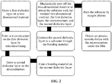
FIG. 2 is a flowchart illustrating preparation of an atomic-smooth device with a microstructure under a film according to present disclosure; -
FIG. 3 is a flowchart illustrating preparation of a device with a microstructure through the existing process; -
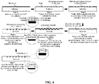
FIG. 4 is a schematic diagram illustrating that burrs and pits are generated during preparation of an atomic-smooth device through an existing etching method; and -
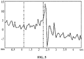
FIG. 5 is an atomic force microscopy (AFM) scanning sectional diagram of a device surface obtained through an existing etching method. - Embodiment for preparation of an atomic-smooth device with metal electrodes under a film
- A structure shown in
step 8 ofFIG. 1 is an atomic-smooth device with a metal electrode in this embodiment. The device includes, from bottom to top, a sapphire substrate, ultraviolet (UV)-curable glue, a second silicon oxide layer on the substrate, an Au electrode array arranged according to application requirements, and a first silicon oxide layer. A surface of the first silicon oxide layer is an atomic-smooth surface and has a diameter of 1 to 100 µm, and an Au electrode array under the first silicon oxide layer does not react with the first silicon oxide layer and the second silicon oxide layer. The edge of the atomic-smooth device has no burrs and the inner of the atomic-smooth device has no protrusions or pits at least within a range of 10 µm × 10 µm. - In conjunction with
FIGS. 1 and2 , a method for preparing a device according to an embodiment of the present disclosure is described, and the case where silicon oxide is used as insulating dielectric material, Au is used as a metal electrode, UV-curable glue is used as the binder, and sapphire is used as the substrate is used as an example. As shown inFIG. 1 , first, HOPG is dissociated to obtain a new smooth surface; a 100nm-thick first dielectric layer silicon oxide is next grown on the new smooth surface at low temperature; metal electrode plates of a capacitive superlubricity generator such as a 6×6×0.2µm3 Au electrode array with an electrode interval of 6 µm are then made on silicon oxide; a 500nm-thick second dielectric layer silicon oxide is then grown at low temperature and can completely cover the Au electrode array; a drop of UV-curable glue is then dripped on a silicon oxide surface of the second dielectric layer, and a glue dispenser is used to make the glue thickness about 100 µm; the UV-curable glue is then covered with a 1mm-thick sapphire sheet with a size equivalent to the HOPG, the UV-curable glue is irradiated with a UV lamp so that the UV-curable glue and the sapphire sheet are bonded, and after irradiated for 1 min, the UV-curable glue is cured; since the HOPG is a layered material and the interlayer dissociation energy is relatively low, when the HOPG and sapphire are dissociated by the mechanical peeling method, the UV-curable glue, the second dielectric layer silicon oxide, Au electrodes, a silicon oxide film of the first dielectric layer, and part of the HOPG remain on the sapphire; the residual HOPG on the sapphire is finally bombarded with O2--Plasma, and the bombardment time depends on the thickness of the residual HOPG. O2- does not react with silicon oxide, so after the HOPG is removed, a large-area atomic-smooth device with metal electrodes under the film may be obtained. The surface of the device is observed to be atomic-smooth under an atomic force microscope. - The large-area atomic-smooth device with the microstructure under the film prepared and obtained in the present disclosure has a diameter of up to 100 µm. The preparation method is simple and convenient, so as to effectively avoid pits or burrs generated when the existing microstructure is machined. Since a polishing process is not performed on surfaces of heterogeneous structures, the use of ultra-high-demand polishing equipment and processing technology in order to obtain a superlubricity smooth surface is avoided, thereby ensuring wide applicability.
- Comparative embodiment for preparation of a device with metal electrodes by the existing etching method
- In conjunction with
FIGS. 3 ,4 and5 , the preparation method and effect in the comparative embodiment of the present disclosure are described below, and the case of a silicon oxide substrate and Au electrodes is used as an example.FIG. 3 is a flowchart illustrating preparation of a device with a microstructure through the existing process. A layer of photoresist is first spin-coated on the silicon oxide substrate, a mask is used to expose the photoresist-coated substrate, and then a developer is used to wash off the exposed photoresist to form the pattern of the subsequent metal electrodes; then photolithography is performed to remove the silicon oxide of the metal electrode pattern on the silicon oxide substrate, that is, the vacant metal electrode pattern is pre-etched; then Au is evaporated on the vacant silicon oxide substrate, and a thickness of the evaporation is approximately the same as a thickness of the etching; then peeling off is performed, that is, a solution such as acetone is used to react with the photoresist to remove the photoresist and Au evaporated on the photoresist; then an insulating layer of silicon oxide is grown on the substrate to cover Au and silicon oxide. -
FIG. 4 is a schematic diagram illustrating that burrs and pits are generated during preparation of an atomic-smooth device through an existing etching method. Due to different adsorption properties of the grown silicon oxide for Au and the silicon oxide substrate, growth rates of the grown silicon oxide on Au and the silicon oxide substrate are also different, resulting in some burrs or pits at the junction of Au and the silicon oxide substrate, thereby causing the junction to be not smooth. As shown inFIG. 5 , the undulation is about tens of nanometers so that the atomic-smooth surface cannot be formed on the final device surface with the microstructure, especially at the edge. That is to say, it is difficult for the heterogeneous material layer to satisfy requirements of atomic-smooth, and it is difficult to achieve the atomic-smooth device with the microstructure under the film. Therefore, from the perspective of the existing common process means, it is difficult to solve the above-mentioned tens of nanometer protrusions or burrs so that requirements of the atomic-smooth surface cannot be satisfied. - The above are only preferred embodiments of the present disclosure. Any equivalent variations or modification made according to the scope of the claims in the present disclosure should belong to the coverage scope of the claims in the present disclosure.
Claims (10)
- An atomic-smooth device with a microstructure, comprising:a substrate, a bonding material, a second dielectric layer on the substrate, the microstructure, and a first dielectric layer in sequence,wherein a surface of the first dielectric layer is an atomic-smooth surface.
- The atomic-smooth device of claim 1, whereinthe atomic-smooth surface has a diameter of 1 to 100 µm;preferably, the microstructure, the first dielectric layer, and the second dielectric layer are heterogeneous materials, and no reaction occurs between the microstructure and the dielectric layers; andan edge of the atomic-smooth device has no burrs and an inner of the atomic-smooth device has no burrs or pits at least within a range of 10 µm × 10 µm.
- The atomic-smooth device of claim 1 or 2, whereinthe first dielectric layer has a thickness of 2 to 100 nm; andboth the first dielectric layer and the second dielectric layer are preferably insulating layers and more preferably silicon oxide layers and preferably prepared by deposition.
- The atomic-smooth device of claim 1 or 2, whereinthe microstructure is a metal electrode and preferably Aurum, Au, Cuprum, Cu, or Argentum, Ag; andthe metal electrode preferably has a thickness of 10 to 150 nm and more preferably 20 to 50 nm.
- A method for preparing the atomic-smooth device with the microstructure of claim 1, comprising:in step 1, growing the first dielectric layer on a surface of a two-dimensional material to obtain an atomic-smooth film;in step 2, preparing the microstructure on the first dielectric layer by micromachining;in step 3, growing the second dielectric layer on the microstructure;in step 4, coating the bonding material on the second dielectric layer;in step 5, connecting the second dielectric layer to the substrate through the bonding material;in step 6, peeling off the two-dimensional material to obtain the substrate having a small amount of residual two-dimensional material, the first dielectric layer, the microstructure, the second dielectric layer, and the bonding material;in step 7, removing the small amount of residual two-dimensional material on the substrate by oxygen plasma etching; andin step 8, obtaining the atomic-smooth device with the microstructure.
- The method of claim 5, whereinthe two-dimensional material is preferably graphene or highly oriented pyrolytic graphite, HOPG, andboth the first dielectric layer and the second dielectric layer are preferably insulating layers and more preferably silicon oxide layers and preferably prepared by deposition.
- The method of claim 5 or 6, whereinthe microstructure is a metal electrode and preferably Aurum, Au, Cuprum, Cu, or Argentum, Ag, andmore preferably, the metal electrode has a thickness of 10 to 150 nm and more preferably 20 to 50 nm.
- The method of any one of claims 5 to 7, wherein the bonding material is selected from at least one of ultraviolet, UV,-curable glue or resin.
- The method of any one of claims 5 to 8, wherein the substrate is selected from one or a combination of Silicon, Si, Silicon Carbide, SiC, Silicon-On-Insulator, SOI, sapphire, mica, graphene, or molybdenum disulfide.
- The method of any one of claims 4 to 9, wherein the atomic-smooth film has a diameter of 1 µm to 100 µm.
Applications Claiming Priority (1)
| Application Number | Priority Date | Filing Date | Title |
|---|---|---|---|
| PCT/CN2020/098480 WO2022000123A1 (en) | 2020-06-28 | 2020-06-28 | Atomic-scale leveling device with microstructure, and method for preparing same |
Publications (2)
| Publication Number | Publication Date |
|---|---|
| EP4113583A1 true EP4113583A1 (en) | 2023-01-04 |
| EP4113583A4 EP4113583A4 (en) | 2023-05-03 |
Family
ID=79317770
Family Applications (1)
| Application Number | Title | Priority Date | Filing Date |
|---|---|---|---|
| EP20942599.0A Pending EP4113583A4 (en) | 2020-06-28 | 2020-06-28 | ATOMIC-SCALE LEVELING DEVICE WITH MICROSTRUCTURE, AND METHOD FOR PREPARING IT |
Country Status (6)
| Country | Link |
|---|---|
| US (1) | US20230271825A1 (en) |
| EP (1) | EP4113583A4 (en) |
| JP (1) | JP7388666B2 (en) |
| KR (1) | KR102781882B1 (en) |
| CN (1) | CN115004343B (en) |
| WO (1) | WO2022000123A1 (en) |
Families Citing this family (1)
| Publication number | Priority date | Publication date | Assignee | Title |
|---|---|---|---|---|
| CN119456361B (en) * | 2024-12-04 | 2025-10-28 | 四川大学 | A process for suppressing burrs in micro-nanostructure processing |
Family Cites Families (30)
| Publication number | Priority date | Publication date | Assignee | Title |
|---|---|---|---|---|
| US6767475B2 (en) * | 2000-05-25 | 2004-07-27 | Atomic Telecom | Chemical-organic planarization process for atomically smooth interfaces |
| EP1535315B1 (en) * | 2002-09-06 | 2010-11-24 | Fraunhofer-Gesellschaft zur Förderung der angewandten Forschung e.V. | Glass-type planar substrate, use thereof, and method for the production thereof |
| SG195119A1 (en) * | 2011-05-23 | 2013-12-30 | Univ Singapore | Method of transferring thin films |
| US8518491B2 (en) * | 2011-07-14 | 2013-08-27 | The United States Of America, As Represented By The Secretary Of The Navy | Preparation of epitaxial graphene surfaces for atomic layer deposition of dielectrics |
| US9139420B2 (en) * | 2012-04-18 | 2015-09-22 | Taiwan Semiconductor Manufacturing Company, Ltd. | MEMS device structure and methods of forming same |
| CN102684546B (en) * | 2012-05-15 | 2015-03-18 | 纳米新能源(唐山)有限责任公司 | Friction generator |
| KR20130132103A (en) * | 2012-05-25 | 2013-12-04 | 삼성테크윈 주식회사 | Method for manufacturing circuit board by using graphene |
| CN202818150U (en) * | 2012-09-20 | 2013-03-20 | 纳米新能源(唐山)有限责任公司 | Nano friction generator |
| CA2918872A1 (en) * | 2013-07-26 | 2015-01-29 | Jx Nippon Oil & Energy Corporation | Method for manufacturing substrate having textured structure |
| CN103824566B (en) * | 2014-03-18 | 2016-08-24 | 清华大学 | The read-write magnetic head of contact hard disk, hard disc apparatus and transfer method |
| WO2015174797A1 (en) * | 2014-05-15 | 2015-11-19 | 주식회사 엘지화학 | Organic light emitting device |
| CN105679647B (en) * | 2015-12-31 | 2018-06-29 | 清华大学 | The preparation method of substrate with atomically flating surface |
| KR101723769B1 (en) | 2016-02-17 | 2017-04-05 | 원광대학교산학협력단 | Direct Transfer Method of Graphene and Method for Selective Atomic Layer Deposition onto Graphene Layer |
| US10622247B2 (en) * | 2016-02-19 | 2020-04-14 | Globalwafers Co., Ltd. | Semiconductor on insulator structure comprising a buried high resistivity layer |
| CN109791876B (en) | 2016-05-12 | 2023-08-15 | 环球晶圆股份有限公司 | Direct Formation of Hexagonal Boron Nitride on Silicon-Based Dielectrics |
| CN106399929B (en) * | 2016-09-28 | 2018-10-30 | 常州工学院 | A kind of atomically flating Sr/Si(100)The preparation method on -2 × 3 structure surfaces again |
| KR20180091569A (en) * | 2017-02-07 | 2018-08-16 | 주식회사 가온인터내셔널 | Method for manufacturing pattern using graphene |
| CN106896088A (en) * | 2017-03-31 | 2017-06-27 | 王利兵 | A kind of preparation method of super even curface plasma resonance chip |
| JP2018202508A (en) * | 2017-05-31 | 2018-12-27 | 国立研究開発法人産業技術総合研究所 | Manufacturing method of substrate with three-dimensional structure |
| CN109148157B (en) * | 2017-06-16 | 2022-01-07 | 深圳清力技术有限公司 | Composite capacitor structure and preparation method and application thereof |
| KR102049323B1 (en) * | 2017-07-05 | 2019-11-27 | 재단법인 나노기반소프트일렉트로닉스연구단 | Nanopatch graphene composite and method for preparing the same |
| CN108456850B (en) * | 2018-03-07 | 2020-06-23 | 深圳大学 | A sandwich structure film and its preparation method and application |
| KR102237576B1 (en) * | 2018-03-28 | 2021-04-07 | 한양대학교 산학협력단 | Electric device using reaction of sacrificial film containing graphene oxide and water, and manufacturing method thereof |
| CN110146113A (en) * | 2018-04-24 | 2019-08-20 | 北京纳米能源与系统研究所 | Self-propelled Hall vehicle sensor based on triboelectric nanogenerator |
| CN109585269B (en) * | 2018-11-09 | 2020-06-26 | 北京大学 | A method for preparing a semiconductor single crystal substrate using a two-dimensional crystal transition layer |
| CN109949832B (en) * | 2019-03-26 | 2021-06-04 | 北京清正泰科技术有限公司 | Contact type magnetic head slider formed based on ultra-smooth structure |
| CN110350819B (en) * | 2019-06-22 | 2020-10-23 | 深圳清华大学研究院 | Electrostatic generator based on ultra-smooth material |
| CN110542942B (en) * | 2019-08-22 | 2021-09-03 | 武汉理工大学 | Optical band asymmetric metamaterial polarization regulator and manufacturing method thereof |
| US11551921B1 (en) * | 2019-09-25 | 2023-01-10 | National Technology & Engineering Solutions Of Sandia, Llc | Miniaturized vacuum package and methods of making same |
| CN213738598U (en) * | 2020-06-28 | 2021-07-20 | 深圳清华大学研究院 | An atomically flat device with microstructures |
-
2020
- 2020-06-28 JP JP2022559671A patent/JP7388666B2/en active Active
- 2020-06-28 US US17/923,648 patent/US20230271825A1/en active Pending
- 2020-06-28 EP EP20942599.0A patent/EP4113583A4/en active Pending
- 2020-06-28 CN CN202080092515.2A patent/CN115004343B/en active Active
- 2020-06-28 KR KR1020227039171A patent/KR102781882B1/en active Active
- 2020-06-28 WO PCT/CN2020/098480 patent/WO2022000123A1/en not_active Ceased
Also Published As
| Publication number | Publication date |
|---|---|
| CN115004343A (en) | 2022-09-02 |
| JP7388666B2 (en) | 2023-11-29 |
| WO2022000123A1 (en) | 2022-01-06 |
| KR20220166850A (en) | 2022-12-19 |
| US20230271825A1 (en) | 2023-08-31 |
| EP4113583A4 (en) | 2023-05-03 |
| CN115004343B (en) | 2025-02-28 |
| JP2023520429A (en) | 2023-05-17 |
| KR102781882B1 (en) | 2025-03-18 |
Similar Documents
| Publication | Publication Date | Title |
|---|---|---|
| CN111505767B (en) | Preparation method of lithium niobate photonic chip based on silicon oxide mask | |
| US6020215A (en) | Process for manufacturing microstructure | |
| CN108461622B (en) | Method for manufacturing piezoelectric sensor and piezoelectric sensor using the same | |
| CN103023371A (en) | Micro-nano integrated generator and manufacturing method thereof | |
| CN104701146A (en) | Graphene nano-electronical appliance and preparation method thereof | |
| US8829436B2 (en) | Phase plate and method of fabricating same | |
| CN111071986A (en) | A method for preparing silicon carbide multilevel microstructure assisted by laser modification and an acceleration sensor | |
| US20230271825A1 (en) | Atomic-smooth device with microstructure, and method for preparing same | |
| CN101359701A (en) | A method for preparing localized back contacts of crystalline silicon solar cells based on nanoimprinting technology | |
| CN213738598U (en) | An atomically flat device with microstructures | |
| RU2469369C2 (en) | X-ray lithographic template and method for production thereof | |
| KR101971825B1 (en) | Large scale graphene liquid cell, and large scale graphene liquid cell fabrication method | |
| CN101825842A (en) | Method for manufacturing nano-imprinting seal | |
| CN111071984B (en) | Method for preparing micro-nano structure by selectively stripping photoresist | |
| CN107871705B (en) | Manufacturing method of high-precision ultrathin THz thin-film circuit | |
| CN111115563A (en) | A kind of method of fully dry functional material stripping | |
| CN101083301A (en) | A method for preparing an organic molecular device with a nanoscale cross wire array structure | |
| JP3120783B2 (en) | Method of manufacturing mask for LIGA process | |
| CN113064227B (en) | Preparation method of sinusoidal grating | |
| CN101734619B (en) | Method for preparing material with highly gradient surface micronano structure | |
| JP3945561B2 (en) | Method for producing extraction electrode | |
| CN102040185B (en) | Manufacturing method of load bearing wafer and load bearing wafer | |
| CN113707357B (en) | Preparation method of high-aspect-ratio zone plate | |
| CN103523743A (en) | Miniature friction energy harvester and method for manufacturing same | |
| US9152036B2 (en) | X-ray mask structure and method for preparing the same |
Legal Events
| Date | Code | Title | Description |
|---|---|---|---|
| STAA | Information on the status of an ep patent application or granted ep patent |
Free format text: STATUS: THE INTERNATIONAL PUBLICATION HAS BEEN MADE |
|
| PUAI | Public reference made under article 153(3) epc to a published international application that has entered the european phase |
Free format text: ORIGINAL CODE: 0009012 |
|
| STAA | Information on the status of an ep patent application or granted ep patent |
Free format text: STATUS: REQUEST FOR EXAMINATION WAS MADE |
|
| 17P | Request for examination filed |
Effective date: 20220930 |
|
| AK | Designated contracting states |
Kind code of ref document: A1 Designated state(s): AL AT BE BG CH CY CZ DE DK EE ES FI FR GB GR HR HU IE IS IT LI LT LU LV MC MK MT NL NO PL PT RO RS SE SI SK SM TR |
|
| REG | Reference to a national code |
Ref country code: DE Ref legal event code: R079 Free format text: PREVIOUS MAIN CLASS: H01L0021480000 Ipc: B81C0001000000 |
|
| STAA | Information on the status of an ep patent application or granted ep patent |
Free format text: STATUS: EXAMINATION IS IN PROGRESS |
|
| A4 | Supplementary search report drawn up and despatched |
Effective date: 20230331 |
|
| RIC1 | Information provided on ipc code assigned before grant |
Ipc: B82Y 40/00 20110101ALI20230327BHEP Ipc: H01L 21/48 20060101ALI20230327BHEP Ipc: B81C 1/00 20060101AFI20230327BHEP |
|
| 17Q | First examination report despatched |
Effective date: 20230417 |
|
| DAV | Request for validation of the european patent (deleted) | ||
| DAX | Request for extension of the european patent (deleted) | ||
| GRAP | Despatch of communication of intention to grant a patent |
Free format text: ORIGINAL CODE: EPIDOSNIGR1 |
|
| STAA | Information on the status of an ep patent application or granted ep patent |
Free format text: STATUS: GRANT OF PATENT IS INTENDED |