EP4105709B1 - Optische abtastvorrichtung, antriebsverfahren einer optischen abtastvorrichtung und bildzeichnungssystem - Google Patents
Optische abtastvorrichtung, antriebsverfahren einer optischen abtastvorrichtung und bildzeichnungssystem Download PDFInfo
- Publication number
- EP4105709B1 EP4105709B1 EP22173297.7A EP22173297A EP4105709B1 EP 4105709 B1 EP4105709 B1 EP 4105709B1 EP 22173297 A EP22173297 A EP 22173297A EP 4105709 B1 EP4105709 B1 EP 4105709B1
- Authority
- EP
- European Patent Office
- Prior art keywords
- time
- angle
- axis
- mirror portion
- signal
- Prior art date
- Legal status (The legal status is an assumption and is not a legal conclusion. Google has not performed a legal analysis and makes no representation as to the accuracy of the status listed.)
- Active
Links
Images


Classifications
-
- G—PHYSICS
- G02—OPTICS
- G02B—OPTICAL ELEMENTS, SYSTEMS OR APPARATUS
- G02B26/00—Optical devices or arrangements for the control of light using movable or deformable optical elements
- G02B26/08—Optical devices or arrangements for the control of light using movable or deformable optical elements for controlling the direction of light
- G02B26/0816—Optical devices or arrangements for the control of light using movable or deformable optical elements for controlling the direction of light by means of one or more reflecting elements
- G02B26/0833—Optical devices or arrangements for the control of light using movable or deformable optical elements for controlling the direction of light by means of one or more reflecting elements the reflecting element being a micromechanical device, e.g. a MEMS mirror, DMD
- G02B26/0858—Optical devices or arrangements for the control of light using movable or deformable optical elements for controlling the direction of light by means of one or more reflecting elements the reflecting element being a micromechanical device, e.g. a MEMS mirror, DMD the reflecting means being moved or deformed by piezoelectric means
-
- G—PHYSICS
- G02—OPTICS
- G02B—OPTICAL ELEMENTS, SYSTEMS OR APPARATUS
- G02B26/00—Optical devices or arrangements for the control of light using movable or deformable optical elements
- G02B26/08—Optical devices or arrangements for the control of light using movable or deformable optical elements for controlling the direction of light
- G02B26/10—Scanning systems
- G02B26/101—Scanning systems with both horizontal and vertical deflecting means, e.g. raster or XY scanners
-
- G—PHYSICS
- G02—OPTICS
- G02B—OPTICAL ELEMENTS, SYSTEMS OR APPARATUS
- G02B26/00—Optical devices or arrangements for the control of light using movable or deformable optical elements
- G02B26/08—Optical devices or arrangements for the control of light using movable or deformable optical elements for controlling the direction of light
- G02B26/10—Scanning systems
- G02B26/105—Scanning systems with one or more pivoting mirrors or galvano-mirrors
-
- G—PHYSICS
- G02—OPTICS
- G02B—OPTICAL ELEMENTS, SYSTEMS OR APPARATUS
- G02B7/00—Mountings, adjusting means, or light-tight connections, for optical elements
- G02B7/18—Mountings, adjusting means, or light-tight connections, for optical elements for prisms; for mirrors
- G02B7/182—Mountings, adjusting means, or light-tight connections, for optical elements for prisms; for mirrors for mirrors
- G02B7/1821—Mountings, adjusting means, or light-tight connections, for optical elements for prisms; for mirrors for mirrors for rotating or oscillating mirrors
-
- H—ELECTRICITY
- H04—ELECTRIC COMMUNICATION TECHNIQUE
- H04N—PICTORIAL COMMUNICATION, e.g. TELEVISION
- H04N9/00—Details of colour television systems
- H04N9/12—Picture reproducers
- H04N9/31—Projection devices for colour picture display, e.g. using electronic spatial light modulators [ESLM]
- H04N9/3129—Projection devices for colour picture display, e.g. using electronic spatial light modulators [ESLM] scanning a light beam on the display screen
- H04N9/3135—Driving therefor
-
- H—ELECTRICITY
- H04—ELECTRIC COMMUNICATION TECHNIQUE
- H04N—PICTORIAL COMMUNICATION, e.g. TELEVISION
- H04N9/00—Details of colour television systems
- H04N9/12—Picture reproducers
- H04N9/31—Projection devices for colour picture display, e.g. using electronic spatial light modulators [ESLM]
- H04N9/3191—Testing thereof
- H04N9/3194—Testing thereof including sensor feedback
Definitions
- the present disclosure relates to an optical scanning device, a driving method of an optical scanning device, and an image drawing system.
- a micromirror device (also referred to as a microscanner) is known as one of micro electro mechanical systems (MEMS) devices manufactured using the silicon (Si) microfabrication technique.
- MEMS micro electro mechanical systems
- An optical scanning device comprising the micromirror device is small and has low power consumption. Thus, applications in image drawing systems such as laser displays or laser projectors are expected.
- a mirror portion is formed to be capable of swinging around a first axis and a second axis that are orthogonal to each other, and light reflected by the mirror portion is two-dimensionally scanned by the swing of the mirror portion around each axis.
- a micromirror device that enables Lissajous scanning of light by causing a mirror portion to resonate around each axis has been known.
- JP2010-256774A discloses a micromirror device comprising a protective member that protects a mirror portion and is provided in a reflection direction of light by the mirror portion to transmit the light reflected by the mirror portion, and a photodetector that is provided across from an inside of a range of transmission of the light reflected by the mirror portion to an outside of the range in the protective member.
- This micromirror device controls an amplitude of the mirror portion in accordance with a detection state of the light by the photodetector.
- WO2014/097683A discloses an optical scanning device comprising a photodetector for detecting angle information of a mirror portion.
- US 2020/314395 A1 discloses a controllable for a tiltable MEMS reflector configured to oscillate the reflector about X axis or about X and Y axes.
- JP 2020016720 A discloses an optical scan device comprising: an optical deflector that causes a mirror part to reflect collimater light, and causes reflected light to exit as scanning light; an optical detection device that is disposed in a rim part of a scan range of the scanning light; a calibration unit that detects a passing time when the scanning light passes through a prescribed location in the scan direction on the basis of an output of the optical detection device, and detects a scan deviation of the scanning light on the basis of the passing time; and a MEMS control unit that controls the optical deflector on the basis of the detected scan deviation.
- EP 1455217 A1 discloses an optical scanning device, a correction method of the position of an image, an image display method, and an image display device able to improve a light projection efficiency and lower the electric power and able to reduce error of the projection image along with an increase in efficiency of light projection in an image display device for scanning by a one-dimensional image to generate a two-dimensional image.
- JP 2010079198 A discloses an image projection device including: an image modulator generating the light beam in which the light emission of a light source part is modulated on the basis of an image signal; an optical scanner for performing outward and homeward scanning by a reflective surface for oscillating the light beam; a reference timing generation part generating the reference timing for causing the light source part to emit light; a light emission timing correction part correcting the light emission start timing of the light beam in each of outward and homeward paths on the basis of the reference timing; and a photosensor detecting the light beam in the outward and homeward paths.
- JP 2012063413 A discloses an optical scanner including: a movable plate with a reflection plane; a pair of torsion beams; two pairs of cantilevers; a support frame; sensor parts by which a mechanical potential generated according to displacement of the movable plate is converted into an electric signal.
- an irradiation timing of light by a light source that irradiates the mirror portion with the light is controlled based on a reference signal (for example, a zero cross signal) representing that the angle of the mirror portion is equal to a reference angle. That is, in a case where sensing accuracy of a timing at which the angle of the mirror portion is equal to the reference angle by the optical scanning device is decreased, image quality of a drawn image is decreased.
- a reference signal for example, a zero cross signal
- the present disclosure is conceived in view of the above matter, and an object thereof is to provide an optical scanning device, a driving method of an optical scanning device, and an image drawing system that can suppress a decrease in image quality of a drawn image.
- This object is achieved by providing an optical scanning device according to claim 1, and a driving method according to claim 18.
- An optical scanning device is an optical scanning device comprising a mirror portion that has a reflecting surface on which an incidence ray is reflected, a first actuator that causes the mirror portion to swing around a first axis which is in a plane including the reflecting surface at a time of a standstill of the mirror portion, a second actuator that causes the mirror portion to swing around a second axis which is in the plane including the reflecting surface at the time of the standstill of the mirror portion and intersects with the first axis, a first angle detection sensor that outputs a signal corresponding to an angle of the mirror portion around the first axis, a second angle detection sensor that outputs a signal corresponding to an angle of the mirror portion around the second axis, at least one photodetector provided at a position at which reflected light from the mirror portion is receivable, and at least one processor, in which the processor is configured to provide a first driving signal having a first driving frequency to the first actuator, provide a second driving signal having a second driving frequency
- one photodetector may be provided at a center of a region in which an image is drawn by the reflected light from the mirror portion.
- the photodetector may be provided on an axis corresponding to the first axis and on an axis corresponding to the second axis in a region in which an image is drawable by the reflected light from the mirror portion.
- At least one photodetector may be provided in each end part on the axis corresponding to the first axis and each end part on the axis corresponding to the second axis in the region in which the image is drawable by the reflected light from the mirror portion.
- the processor is configured to derive a first average phase delay time by averaging a first phase delay time of the output signal of the first angle detection sensor with respect to the first driving signal in a plurality of cycles, and derive a second average phase delay time by averaging a second phase delay time of the output signal of the second angle detection sensor with respect to the second driving signal in a plurality of cycles,
- the point in time when the output signal of the first angle detection sensor represents that the angle of the mirror portion around the first axis is equal to the first reference angle may be a point in time after an elapse of the first average phase delay time from a point in time when the first driving signal represents that the angle of the mirror portion around the first axis is equal to the first reference angle
- the point in time when the output signal of the second angle detection sensor represents that the angle of the mirror portion around the second axis is equal to the second reference angle may be a point in time after an elapse of the second average phase delay time from a
- the processor may be configured to derive the first average phase delay time by averaging the first phase delay time at a point in time when the output signal of the first angle detection sensor is zero, and derive the second average phase delay time by averaging the second phase delay time at a point in time when the output signal of the second angle detection sensor is zero.
- the processor may be configured to derive the first average phase delay time by averaging the first phase delay time from a point in time when the first driving signal is zero to the point in time when the output signal of the first angle detection sensor is zero in a corresponding cycle, and derive the second average phase delay time by averaging the second phase delay time from a point in time when the second driving signal is zero to the point in time when the output signal of the second angle detection sensor is zero in a corresponding cycle.
- the first reference angle and the second reference angle may be zero
- the first shift time may be a time from a point in time when the output signal of the first angle detection sensor represents that the angle of the mirror portion around the first axis is zero to a point in time when the output signal of the photodetector represents that the angle of the mirror portion around the first axis is zero
- the second shift time may be a time from a point in time when the output signal of the second angle detection sensor represents that the angle of the mirror portion around the second axis is zero to a point in time when the output signal of the photodetector represents that the angle of the mirror portion around the second axis is zero.
- the processor may be configured to generate the first reference signal at a point in time after an elapse of the first shift time from the point in time when the output signal of the first angle detection sensor represents that the angle of the mirror portion around the first axis is equal to the first reference angle, and generate the second reference signal at a point in time after an elapse of the second shift time from the point in time when the output signal of the second angle detection sensor represents that the angle of the mirror portion around the second axis is equal to the second reference angle.
- a shift time derivation mode in which the first shift time and the second shift time are derived may be provided, and the processor may be configured to acquire the first shift time and the second shift time for each preset condition by executing the shift time derivation mode in calibration, and use the first shift time and the second shift time acquired in advance in the calibration in generating the first reference signal and the second reference signal.
- the condition may include the first phase delay time and the second phase delay time.
- the condition may further include a driving voltage of the first driving signal and a driving voltage of the second driving signal.
- condition may further include the first driving frequency and the second driving frequency.
- the condition may further include an ambient temperature.
- the photodetector may be a photodiode.
- the photodetector may be in a non-driven state during drawing of an image.
- the first angle detection sensor may include a pair of angle detection sensors arranged at positions that face each other with the first axis or the second axis interposed between the positions
- the output signal of the first angle detection sensor may be an output signal obtained by adding or subtracting a pair of output signals output from the pair of angle detection sensors
- the second angle detection sensor may include a pair of angle detection sensors arranged at positions that face each other with the first axis or the second axis interposed between the positions
- the output signal of the second angle detection sensor may be an output signal obtained by adding or subtracting a pair of output signals output from the pair of angle detection sensors.
- an image drawing system comprises above any optical scanning device, and a light source that irradiates the mirror portion with light.
- a driving method of an optical scanning device is a driving method of an optical scanning device including a mirror portion that has a reflecting surface on which an incidence ray is reflected, a first actuator that causes the mirror portion to swing around a first axis which is in a plane including the reflecting surface at a time of a standstill of the mirror portion, a second actuator that causes the mirror portion to swing around a second axis which is in the plane including the reflecting surface at the time of the standstill of the mirror portion and intersects with the first axis, a first angle detection sensor that outputs a signal corresponding to an angle of the mirror portion around the first axis, a second angle detection sensor that outputs a signal corresponding to an angle of the mirror portion around the second axis, and at least one photodetector provided at a position at which reflected light from the mirror portion is receivable, the driving method comprising providing a first driving signal having a first driving frequency to the first actuator, providing a second driving signal
- a decrease in image quality of a drawn image can be suppressed.
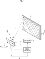
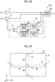
- the image drawing system 10 includes an optical scanning device 2 and a light source 3.
- the optical scanning device 2 includes a micromirror device (hereinafter, referred to as an "MMD") 4, a driving controller 5, and a photodetector 7.
- the driving controller 5 is an example of a processor according to the embodiment of the technique of the disclosure.
- the image drawing system 10 draws an image by optically scanning a surface to be scanned 6 by reflecting a light beam L of irradiation from the light source 3 by the MMD 4 under control of the driving controller 5.
- the surface to be scanned 6 is, for example, a screen for projecting the image, or a retina of an eye of a person.
- the image drawing system 10 is applied to, for example, a Lissajous scanning type laser display.
- the image drawing system 10 can be applied to a laser scanning display such as augmented reality (AR) glasses or virtual reality (VR) glasses.
- AR augmented reality
- VR virtual reality
- the MMD 4 is a piezoelectric biaxial drive type micromirror device capable of causing a mirror portion 20 (see Fig. 2 ) to swing around a first axis a 1 and a second axis a 2 orthogonal to the first axis a 1 .
- a direction parallel to the second axis a 2 will be referred to as an X direction
- a direction parallel to the first axis a 1 will be referred to as a Y direction
- a direction orthogonal to the first axis a 1 and the second axis a 2 will be referred to as a Z direction.
- first axis a 1 may intersect with the second axis a 2 at an angle other than 90°.
- intersecting means being within a constant angle range centered at 90 degrees including an allowable error.
- the light source 3 is a laser device that emits, for example, laser light as the light beam L.
- the light source 3 outputs laser light of three colors of red (R), green (G), and blue (B).
- R red
- G green
- B blue
- the light source 3 perpendicularly irradiates a reflecting surface 20A (see Fig. 2 ) comprised in the mirror portion 20 with the light beam L in a state where the mirror portion 20 of the MMD 4 is at a standstill.
- the reflecting surface 20A is perpendicularly irradiated with the light beam L from the light source 3
- the light source 3 may be an obstacle in the drawing by scanning the surface to be scanned 6 with the light beam L.
- the reflecting surface 20A is perpendicularly irradiated with the light beam L emitted from the light source 3 by controlling the light beam L by an optical system.
- the optical system may include a lens or may not include a lens.
- an angle at which the reflecting surface 20A is irradiated with the light beam L emitted from the light source 3 is not limited to a perpendicular angle.
- the reflecting surface 20A may be irradiated with the light beam L in an inclined manner.
- the driving controller 5 outputs a driving signal to the light source 3 and the MMD 4 based on optical scanning information.
- the light source 3 generates the light beam L based on the input driving signal and irradiates the MMD 4 with the light beam L.
- the MMD 4 causes the mirror portion 20 to swing around the first axis a 1 and the second axis a 2 based on the input driving signal.
- the mirror portion 20 By causing the mirror portion 20 to resonate around each of the first axis a 1 and the second axis a 2 by the driving controller 5, the light beam L reflected by the mirror portion 20 is scanned onto the surface to be scanned 6 such that the light beam L draws a Lissajous waveform.
- This optical scanning method is called a Lissajous scanning method.
- the photodetector 7 photoelectrically converts an incidence ray and outputs a signal corresponding to a light quantity. As will be described in detail later, the photodetector 7 is not used in the drawing of the image on the surface to be scanned 6 by reflected light from the MMD 4 based on the drawing data and is used in calibration. Examples of the photodetector 7 include a photodiode.
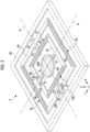
- the MMD 4 includes the mirror portion 20, a first support portion 21, a first movable frame 22, a second support portion 23, a second movable frame 24, a connecting portion 25, and a fixed frame 26.
- the MMD 4 is a so-called MEMS scanner.
- the mirror portion 20 has the reflecting surface 20A for reflecting the incidence ray.
- the reflecting surface 20A is provided on one surface of the mirror portion 20 and is formed with a metal thin film of, for example, gold (Au), aluminum (Al), silver (Ag), or a silver alloy.
- a shape of the reflecting surface 20A is, for example, a circular shape centered at an intersection between the first axis a 1 and the second axis a 2 .
- the first axis a 1 and the second axis a 2 are present in a plane including the reflecting surface 20A at a time of a standstill when the mirror portion 20 is at a standstill.
- a planar shape of the MMD 4 is a rectangular shape and is axially symmetric with respect to the first axis a 1 and axially symmetric with respect to the second axis a 2 .
- the first support portion 21 is arranged outside the mirror portion 20 at each of positions that face each other with the second axis a 2 interposed therebetween.
- the first support portions 21 are connected to the mirror portion 20 on the first axis a 1 and support the mirror portion 20 to be capable of swinging around the first axis a 1 .
- the first support portions 21 are torsion bars that stretch along the first axis a 1 .
- the first movable frame 22 is a frame having a rectangular shape surrounding the mirror portion 20 and is connected to the mirror portion 20 through the first support portion 21 on the first axis a 1 .
- a piezoelectric element 30 is formed on the first movable frame 22 at each of positions that face each other with the first axis a 1 interposed therebetween. In such a manner, a pair of first actuators 31 are configured by forming two piezoelectric elements 30 on the first movable frame 22.
- the pair of first actuators 31 are arranged at positions that face each other with the first axis a 1 interposed therebetween.
- the first actuators 31 cause the mirror portion 20 to swing around the first axis a 1 by applying rotational torque around the first axis a 1 to the mirror portion 20.
- the second support portion 23 is arranged outside the first movable frame 22 at each of positions with the first axis a 1 interposed therebetween.
- the second support portions 23 are connected to the first movable frame 22 on the second axis a 2 and support the first movable frame 22 and the mirror portion 20 to be capable of swinging around the second axis a 2 .
- the second support portions 23 are torsion bars that stretch along the second axis a 2 .
- the second movable frame 24 is a frame having a rectangular shape surrounding the first movable frame 22 and is connected to the first movable frame 22 through the second support portion 23 on the second axis a 2 .
- the piezoelectric element 30 is formed on the second movable frame 24 at each of positions that face each other with the second axis a 2 interposed therebetween. In such a manner, a pair of second actuators 32 are configured by forming two piezoelectric elements 30 on the second movable frame 24.
- the pair of second actuators 32 are arranged at positions that face each other with the second axis a 2 interposed therebetween.
- the second actuators 32 cause the mirror portion 20 to swing around the second axis a 2 by applying rotational torque about the second axis a 2 to the mirror portion 20 and the first movable frame 22.
- the connecting portion 25 is arranged outside the second movable frame 24 at each of positions with the first axis a 1 interposed therebetween.
- the connecting portions 25 are connected to the second movable frame 24 on the second axis a 2 .
- the fixed frame 26 is a frame having a rectangular shape surrounding the second movable frame 24 and is connected to the second movable frame 24 through the connecting portion 25 on the second axis a 2 .
- a pair of first angle detection sensors 11A and 11B are provided in the first movable frame 22 near the first support portions 21 at positions that face each other with the first axis a 1 interposed therebetween.
- Each of the pair of first angle detection sensors 11A and 11B is configured with a piezoelectric element.
- Each of the first angle detection sensors 11A and 11B outputs a signal by converting a force applied by deformation of the first support portion 21 accompanied by rotational movement of the mirror portion 20 around the first axis a 1 into a voltage. That is, the first angle detection sensors 11A and 11B output signals corresponding to an angle of the mirror portion 20 around the first axis a 1 .
- a pair of second angle detection sensors 12A and 12B are provided in the second movable frame 24 near the second support portions 23 at positions that face each other with the second axis a 2 interposed therebetween.
- Each of the pair of second angle detection sensors 12A and 12B is configured with a piezoelectric element.
- Each of the second angle detection sensors 12A and 12B outputs a signal by converting a force applied by deformation of the second support portion 23 accompanied by rotational movement of the mirror portion 20 around the second axis a 2 into a voltage. That is, the second angle detection sensors 12A and 12B output signals corresponding to the angle of the mirror portion 20 around the second axis a 2 .
- wiring lines and electrode pads for providing driving signals to the first actuators 31 and the second actuators 32 are not shown.
- wiring lines and electrode pads for outputting signals from the first angle detection sensors 11A and 11B and the second angle detection sensors 12A and 12B are not shown.
- a plurality of electrode pads are provided on the fixed frame 26.
- a deflection angle (hereinafter, referred to as a "first deflection angle”) ⁇ 1 of the mirror portion 20 around the first axis a 1 is controlled by the driving signal (hereinafter, referred to as a "first driving signal") provided to the first actuators 31 by the driving controller 5.
- the first driving signal is, for example, a sinusoidal alternating current voltage.
- the first driving signal includes a driving voltage waveform V 1A (t) applied to one of the pair of first actuators 31 and a driving voltage waveform V 1B (t) applied to the other.
- the driving voltage waveform V 1A (t) and the driving voltage waveform V 1B (t) are in anti-phase with each other (that is, have a phase difference of 180°).
- the first deflection angle ⁇ 1 is an angle at which a line normal to the reflecting surface 20A is inclined with respect to the Z direction in an XZ plane.
- a deflection angle (hereinafter, referred to as a "second deflection angle") ⁇ 2 of the mirror portion 20 around the second axis a 2 is controlled by the driving signal (hereinafter, referred to as a "second driving signal") provided to the second actuators 32 by the driving controller 5.
- the second driving signal is, for example, a sinusoidal alternating current voltage.
- the second driving signal includes a driving voltage waveform V 2A (t) applied to one of the pair of second actuators 32 and a driving voltage waveform V 2B (t) applied to the other.
- the driving voltage waveform V 2A (t) and the driving voltage waveform V 2B (t) are in anti-phase with each other (that is, have a phase difference of 180°).
- the second deflection angle ⁇ 2 is an angle at which the line normal to the reflecting surface 20A is inclined with respect to the Z direction in a YZ plane.
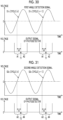
- Fig. 3 shows an example of the first driving signal
- Fig. 4 shows an example of the second driving signal
- Fig. 3 shows the driving voltage waveforms V 1A (t) and V 1B (t) included in the first driving signal
- Fig. 4 shows the driving voltage waveforms V 2A (t) and V 2B (t) included in the second driving signal.
- V 1A (t) and V 1B (t) are represented as follows.
- V 1A t V off1 + V 1 sin 2 ⁇ f d1 t
- V 1B t V off1 + V 1 sin 2 ⁇ f d1 t + ⁇
- V 1 is an amplitude voltage.
- V off1 is a bias voltage.
- V off1 may be zero.
- f d1 is a driving frequency (hereinafter, referred to as a "first driving frequency").
- t is time.
- the mirror portion 20 swings around the first axis a 1 with the first driving frequency f d1 .
- V 2A (t) and V 2B (t) are represented as follows.
- V 2A t V off2 + V 2 sin 2 ⁇ f d2 t + ⁇
- V 2B t V off2 + V 2 sin 2 ⁇ f d2 t + ⁇ + ⁇
- V 2 is an amplitude voltage.
- V off2 is a bias voltage.
- V off2 may be zero.
- f d2 is a driving frequency (hereinafter, referred to as a "second driving frequency").
- t is time.
- ⁇ is a phase difference between the driving voltage waveforms V 1A (t) and V 1B (t) and the driving voltage waveforms V 2A (t) and V 2B (t).
- the mirror portion 20 swings around the second axis a 2 with the second driving frequency f d2 .
- the first driving frequency f d1 is set to match a resonance frequency of the mirror portion 20 around the first axis a 1 .
- the second driving frequency f d2 is set to match the resonance frequency of the mirror portion 20 around the second axis a 2 .
- f d1 > f d2 is assumed. That is, the mirror portion 20 has a higher swing frequency around the first axis a 1 than a swing frequency around the second axis a 2 .
- the first driving frequency f d1 and the second driving frequency f d2 may not necessarily match the resonance frequency.
- each of the first driving frequency f d1 and the second driving frequency f d2 may be a frequency within a frequency range near the resonance frequency (for example, a half-width range of a frequency distribution having the resonance frequency as a peak value).
- this frequency range is within a range of a so-called Q-value.
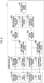
- the driving controller 5 includes a first driving signal generation portion 60A, a second driving signal generation portion 60B, a first signal processing portion 61A, a second signal processing portion 61B, a first phase shift portion 62A, a second phase shift portion 62B, a first derivation portion 63A, a second derivation portion 63B, a third derivation portion 64, a first zero cross pulse output portion 65A, a second zero cross pulse output portion 65B, and a light source driving portion 66.
- the first driving signal generation portion 60A, the first signal processing portion 61A, and the first phase shift portion 62A may perform a feedback control to maintain a vibration state where the swing of the mirror portion 20 around the first axis a 1 has a designated frequency.
- the second driving signal generation portion 60B, the second signal processing portion 61B, and the second phase shift portion 62B may perform a feedback control to maintain a vibration state where the swing of the mirror portion 20 around the second axis a 2 has a designated frequency.
- the first driving signal generation portion 60A generates the first driving signal including the driving voltage waveforms V 1A (t) and V 1B (t) based on a reference waveform and provides the generated first driving signal to the pair of first actuators 31 through the first phase shift portion 62A. Accordingly, the mirror portion 20 swings around the first axis a 1 .
- the second driving signal generation portion 60B generates the second driving signal including the driving voltage waveforms V 2A (t) and V 2B (t) based on the reference waveform and provides the generated second driving signal to the pair of second actuators 32 through the second phase shift portion 62B. Accordingly, the mirror portion 20 swings around the second axis a 2 .
- the first driving signal generated by the first driving signal generation portion 60A and the second driving signal generated by the second driving signal generation portion 60B are synchronized in phase as shown by ⁇ in the expression showing the driving voltage waveforms V 2A (t) and V 2B (t) included in the second driving signal.
- the first angle detection sensors 11A and 11B output the signals corresponding to the angle of the mirror portion 20 around the first axis a 1 .
- the second angle detection sensors 12A and 12B output the signals corresponding to the angle of the mirror portion 20 around the second axis a 2 .
- Fig. 6 shows an example of the signals output from the pair of first angle detection sensors 11A and 11B.
- S1a 1 and S1a 2 represent the signals output from the pair of first angle detection sensors 11A and 11B in a case where the mirror portion 20 is caused to swing around only the first axis a 1 and not swing around the second axis a 2 .
- the signals S1a 1 and S1a 2 are waveform signals similar to a sinusoidal wave having the first driving frequency f d1 and are in anti-phase with each other.
- a vibration noise RN1 caused by the swing of the mirror portion 20 around the second axis a 2 is superimposed on the output signals of the pair of first angle detection sensors 11A and 11B.
- S1b 1 represents a signal after the vibration noise RN1 is superimposed on the signal S1a 1 .
- S1b 2 represents a signal after the vibration noise RN1 is superimposed on the signal S1a 2 .
- the vibration noise RN1 is shown in a highlighted manner for description of the present embodiment.
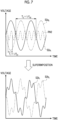
- Fig. 7 shows an example of the signals output from the pair of second angle detection sensors 12A and 12B.
- S2a 1 and S2a 2 represent the signals output from the pair of second angle detection sensors 12A and 12B in a case where the mirror portion 20 is caused to swing around only the second axis a 2 and not swing around the first axis a 1 .
- the signals S2a 1 and S2a 2 are waveform signals similar to a sinusoidal wave having the second driving frequency f d2 and are in anti-phase with each other.
- a vibration noise RN2 caused by the swing of the mirror portion 20 around the first axis a 1 is superimposed on the output signals of the pair of second angle detection sensors 12A and 12B.
- S2b 1 represents a signal obtained by the superimposition of the vibration noise RN2 on the signal S2a 1 .
- S2b 2 represents a signal obtained by the superimposition of the vibration noise RN2 on the signal S2a 2 .
- the vibration noise RN2 is shown in a highlighted manner for description of the present embodiment.
- the first signal processing portion 61A generates a signal (hereinafter, referred to as a "first angle detection signal”) S1c obtained by removing the vibration noise RN1 based on S1a 1 and S1a 2 output from the pair of first angle detection sensors 11A and 11B.
- the second signal processing portion 61B generates a signal (hereinafter, referred to as a "second angle detection signal”) S2c obtained by removing the vibration noise RN2 based on S2a 1 and S2a 2 output from the pair of second angle detection sensors 12A and 12B.
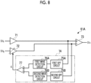
- the first signal processing portion 61A can be implemented by, for example, a circuit having a configuration shown in Fig. 8 as an example. As shown in Fig. 8 , the first signal processing portion 61A is configured with a buffer amplifier 71, a variable gain amplifier 72, a subtraction circuit 73, and a gain adjustment circuit 74.
- the gain adjustment circuit 74 is configured with a first band pass filter (BPF) circuit 75A, a second BPF circuit 75B, a first wave detection circuit 76A, a second wave detection circuit 76B, and a subtraction circuit 77.
- BPF band pass filter
- the subtraction circuit 73 and the subtraction circuit 77 are differential amplification circuits configured with operational amplifiers.
- the signal S1b 1 output from the first angle detection sensor 11A is input into a positive input terminal (non-inverting input terminal) of the subtraction circuit 73 through the buffer amplifier 71.
- a signal output from the buffer amplifier 71 branches in the middle of being input into the subtraction circuit 73 and is input into the first BPF circuit 75A in the gain adjustment circuit 74.
- the signal S1b 2 output from the first angle detection sensor 11B is input into a negative input terminal (inverting input terminal) of the subtraction circuit 73 through the variable gain amplifier 72.
- a signal output from the variable gain amplifier 72 branches in the middle of being input into the subtraction circuit 73 and is input into the second BPF circuit 75B in the gain adjustment circuit 74.
- Each of the first BPF circuit 75A and the second BPF circuit 75B has a passband B1 having the second driving frequency f d2 as a center frequency.
- the passband B1 is a frequency band of f d2 ⁇ 5 kH.
- the vibration noise RN1 has the second driving frequency f d2 and thus, passes through the passband B1. Accordingly, the first BPF circuit 75A extracts the vibration noise RN1 from the signal input from the buffer amplifier 71 and outputs the vibration noise RN1.
- the second BPF circuit 75B extracts the vibration noise RN1 from the signal input from the variable gain amplifier 72 and outputs the vibration noise RN1.
- Each of the first wave detection circuit 76A and the second wave detection circuit 76B is configured with, for example, a root mean squared value to direct current converter (RMS-DC converter).
- the first wave detection circuit 76A converts an amplitude of the vibration noise RN1 input from the first BPF circuit 75A into a DC voltage signal and inputs the DC voltage signal into a positive input terminal of the subtraction circuit 77.
- the second wave detection circuit 76B converts the amplitude of the vibration noise RN1 input from the second BPF circuit 75B into a DC voltage signal and inputs the DC voltage signal into a negative input terminal of the subtraction circuit 77.
- the subtraction circuit 77 outputs a value d 1 obtained by subtracting the DC voltage signal input from the second wave detection circuit 76B from the DC voltage signal input from the first wave detection circuit 76A.
- the value d 1 corresponds to a difference between the amplitude of the vibration noise RN1 included in the signal S1b 1 output from the first angle detection sensor 11A and the amplitude of the vibration noise RN1 included in the signal S1b 2 output from the first angle detection sensor 11B.
- the subtraction circuit 77 inputs the value d 1 into a gain adjustment terminal of the variable gain amplifier 72 as a gain adjustment value.
- the variable gain amplifier 72 adjusts an amplitude level of the signal S1b 2 by multiplying the signal S1b 2 input from the first angle detection sensor 11B by the value d 1 input as the gain adjustment value. In such a manner, by performing a feedback control by the gain adjustment circuit 74, the amplitude of the vibration noise RN1 included in the signal S1b 2 after passing through the variable gain amplifier 72 is adjusted to match the amplitude of the vibration noise RN1 included in the signal S1b 1 after passing through the buffer amplifier 71.
- the subtraction circuit 73 outputs a value obtained by subtracting the signal S1b 2 input to the negative input terminal from the signal S1b 1 input to the positive input terminal. Since the amplitudes of the vibration noises RN1 included in both signals are matched by the feedback control, the vibration noises RN1 included in both signals are offset by subtraction processing performed by the subtraction circuit 73. Accordingly, the first angle detection signal S1c (see Fig. 9 ) that is a signal obtained by removing the vibration noise RN1 is output from the subtraction circuit 73.
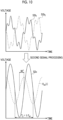
- Fig. 9 shows a state where the first angle detection signal S1c is generated based on S1b 1 and S1b 2 output from the pair of first angle detection sensors 11A and 11B.
- the first angle detection signal S1c corresponds to a signal obtained by doubling an amplitude of the signal obtained by removing the vibration noise RN1 from the signal S1b 1 .
- the first angle detection signal S1c output from the first signal processing portion 61A has a delay of 90° in phase with respect to the driving voltage waveform V 1A (t) included in the first driving signal as shown in Fig. 9 .
- the second signal processing portion 61B can be implemented by the same configuration as the first signal processing portion 61A and thus, will not be described.
- Fig. 10 shows a state where the second angle detection signal S2c is generated based on S2b 1 and S2b 2 output from the pair of second angle detection sensors 12A and 12B.
- the second angle detection signal S2c corresponds to a signal obtained by doubling an amplitude of the signal obtained by removing the vibration noise RN2 from the signal S2b 1 .
- the second angle detection signal S2c output from the second signal processing portion 61B has a delay of 90° in phase with respect to the driving voltage waveform V 2A (t) included in the second driving signal as shown in Fig. 10 .
- the first angle detection signal S1c generated by the first signal processing portion 61A is fed back to the first driving signal generation portion 60A.
- the first phase shift portion 62A shifts phases of the driving voltage waveforms output from the first driving signal generation portion 60A. For example, the first phase shift portion 62A shifts the phases by 90°.
- the second angle detection signal S2c generated by the second signal processing portion 61B is fed back to the second driving signal generation portion 60B.
- the second phase shift portion 62B shifts phases of the driving voltage waveforms output from the second driving signal generation portion 60B. For example, the second phase shift portion 62B shifts the phases by 90°.
- the first angle detection signal S1c generated by the first signal processing portion 61A is ideally a sinusoidal wave but generally not a smooth sinusoidal wave. This is because an influence of the swing of the mirror portion 20 around the second axis a 2 cannot be removed in processing performed by the first signal processing portion 61A.
- a zero cross timing of the first angle detection signal S1c is slightly shifted depending on a cycle.
- waveforms of the zero cross timing of first angle detection signal S1c in a plurality of cycles are superimposed is shown.
- the first derivation portion 63A reduces an influence of the shift for each cycle by averaging the first angle detection signal S1c in the plurality of cycles.
- processing performed by the first derivation portion 63A will be described.
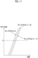
- the first derivation portion 63A derives a first average phase delay time by averaging a phase delay time (hereinafter, referred to as a "first phase delay time") of the first angle detection signal S1c with respect to the first driving signal in the most recent plurality of cycles. Specifically, as shown in Fig. 12 as an example, for the first driving signal and the first angle detection signal S1c in the most recent plurality of cycles, the first derivation portion 63A derives the first average phase delay time by averaging a first phase delay time t1 from a point in time when the first driving signal is zero to a point in time when the first angle detection signal S1c is zero in a corresponding cycle.
- the first driving signal is offset by an amount corresponding to the bias voltage V off1 .
- the point in time when the first driving signal is zero means a point in time when the first driving signal is V off1 .
- the second angle detection signal S2c generated by the second signal processing portion 61B is also ideally a sinusoidal wave but generally not a smooth sinusoidal wave because an influence of the swing of the mirror portion 20 around the first axis a 1 remains. Therefore, the second derivation portion 63B reduces the influence of the shift for each cycle by averaging the second angle detection signal S2c in the plurality of cycles.
- processing performed by the second derivation portion 63B will be described.
- the second derivation portion 63B derives a second average phase delay time by averaging a phase delay time (hereinafter, referred to as a "second phase delay time") of the second angle detection signal S2c with respect to the second driving signal in the most recent plurality of cycles. Specifically, as shown in Fig. 13 as an example, for the second driving signal and the second angle detection signal S2c in the most recent plurality of cycles, the second derivation portion 63B derives the second average phase delay time by averaging a second phase delay time t2 from a point in time when the second driving signal is zero to a point in time when the second angle detection signal S2c is zero in a corresponding cycle.
- the second driving signal is offset by an amount corresponding to the bias voltage V off2 .
- the point in time when the second driving signal is zero means a point in time when the second driving signal is V off2 .
- the present disclosure is not limited thereto.
- a point in time when the sinusoidal wave is zero from a positive value toward a negative value may be used, or both of the point in time when the sinusoidal wave is zero from a negative value toward a positive value and the point in time when the sinusoidal wave is zero from a positive value toward a negative value may be used.
- first shift time t3 1 a shift having a shift time t3 1 (hereinafter, referred to as the "first shift time t3 1 ") may occur between a timing at which the first angle detection signal S1c is zero and an actual timing at which the first deflection angle ⁇ 1 is zero.
- a shift having a shift time t3 2 (hereinafter, referred to as the "second shift time t3 2 ") may occur between a timing at which the second angle detection signal S2c is zero and an actual timing at which the second deflection angle ⁇ 2 is zero.
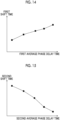
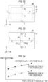
- Fig. 14 shows an example of a relationship between the first average phase delay time and the first shift time t3 1
- Fig. 15 shows an example of a relationship between the second average phase delay time and the second shift time t3 2 .
- the first average phase delay time is increased
- the first shift time t3 1 is increased
- the second average phase delay time is increased
- the second shift time t3 2 is decreased.
- the third derivation portion 64 derives the first shift time t3 1 and the second shift time t3 2 as shift times corresponding to a preset condition.
- first average phase delay time for example, the first phase delay time in the most recent cycle may be used.
- second average phase delay time for example, the second phase delay time in the most recent cycle may be used.
- the third derivation portion 64 derives the first shift time t3 1 corresponding to a first average phase delay time t1 avg in accordance with the following function f1.
- t3 1 f1 t1 avg
- the third derivation portion 64 may derive the first shift time t3 1 corresponding to the first average phase delay time t1 avg using a look-up table in which the first average phase delay time t1 avg is associated with the first shift time t3 1 .
- the third derivation portion 64 derives the second shift time t3 2 corresponding to a second average phase delay time t2 avg in accordance with the following function f2.
- t3 2 f2 t2 avg
- the third derivation portion 64 may derive the second shift time t3 2 corresponding to the second average phase delay time t2 avg using a look-up table in which the second average phase delay time t2 avg is associated with the second shift time t3 2 .
- the function f1 is a function obtained by calibration and is obtained by approximating a relationship between the first average phase delay time and the first shift time t3 1 .
- the function f2 is a function obtained by calibration and is obtained by approximating a relationship between the second average phase delay time and the second shift time t3 2 . Details of the calibration will be described later.
- the first zero cross pulse output portion 65A generates a reference signal (hereinafter, referred to as a "first reference signal") based on the first driving signal, the first average phase delay time derived by the first derivation portion 63A, and the first shift time t3 1 derived by the third derivation portion 64.
- the first reference signal is a signal representing that the angle of the mirror portion 20 around the first axis a 1 is equal to a reference angle (hereinafter, referred to as a first reference angle"). In the present embodiment, an example of applying zero as the first reference angle will be described.
- the first zero cross pulse output portion 65A generates a zero cross pulse (hereinafter, referred to as a "first zero cross pulse”) ZC1 as an example of the first reference signal based on the first driving signal, the first average phase delay time derived by the first derivation portion 63A, and the first shift time t3 1 derived by the third derivation portion 64.
- the first zero cross pulse output portion 65A is configured with a zero cross detection circuit.
- the first zero cross pulse is a zero cross signal representing that the angle of the mirror portion 20 around the first axis a 1 is zero.
- the first shift time t3 1 is a shift time used for correcting a generation timing of the first reference signal.
- the first shift time t3 1 is a shift time of a point in time when the angle of the mirror portion 20 around the first axis a 1 is actually equal to the first reference angle with respect to a point in time (in the present embodiment, a point in time when the first angle detection signal S1c crosses zero) when the first angle detection signal S1c represents that the angle of the mirror portion 20 around the first axis a 1 is equal to the first reference angle (in the present embodiment, zero).
- the point in time when the first angle detection signal S1c represents that the angle of the mirror portion 20 around the first axis a 1 is equal to the first reference angle is a point in time after an elapse of the first average phase delay time from a point in time (in the present embodiment, a point in time when the first driving signal crosses V off1 ) when the first driving signal represents that the angle of the mirror portion 20 around the first axis a 1 is equal to the first reference angle.
- the second zero cross pulse output portion 65B generates a zero cross pulse (hereinafter, referred to as a "second zero cross pulse") ZC2 as an example of the second reference signal based on the second driving signal, the second average phase delay time derived by the second derivation portion 63B, and the second shift time t3 2 derived by the third derivation portion 64.
- the second zero cross pulse output portion 65B is configured with a zero cross detection circuit.
- the second zero cross pulse is a zero cross signal representing that the angle of the mirror portion 20 around the second axis a 2 is zero.
- the second zero cross pulse output portion 65B generates the second zero cross pulse ZC2 at a timing after an elapse of an added time of the second average phase delay time and the second shift time t3 2 from a timing at which the second driving signal crosses zero (in the present embodiment, V off2 ).
- the second zero cross pulse output portion 65B outputs the generated second zero cross pulse ZC2 to the light source driving portion 66.
- the second shift time t3 2 is a shift time used for correcting a generation timing of the second reference signal.
- the second shift time t3 2 is a shift time of a point in time when the angle of the mirror portion 20 around the second axis a 2 is actually equal to the second reference angle with respect to a point in time (in the present embodiment, a point in time when the second angle detection signal S2c crosses zero) when the second angle detection signal S2c represents that the angle of the mirror portion 20 around the second axis a 2 is equal to the second reference angle (in the present embodiment, zero).
- the point in time when the second angle detection signal S2c represents that the angle of the mirror portion 20 around the second axis a 2 is equal to the second reference angle is a point in time after an elapse of the second average phase delay time from a point in time (in the present embodiment, a point in time when the second driving signal crosses V off2 ) when the second driving signal represents that the angle of the mirror portion 20 around the second axis a 2 is equal to the second reference angle.
- first zero cross pulse output portion 65A and the second zero cross pulse output portion 65B output the zero cross pulses using both of the point in time when the sinusoidal wave is zero from a negative value toward a positive value and the point in time when the sinusoidal wave is zero from a positive value toward a negative value
- the present disclosure is not limited thereto.
- the first zero cross pulse output portion 65A and the second zero cross pulse output portion 65B may output the zero cross pulses using any one of the point in time when the sinusoidal wave is zero from a negative value toward a positive value or the point in time when the sinusoidal wave is zero from a positive value toward a negative value.
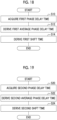
- first shift time derivation processing is executed at a predetermined time interval during the drawing of the image by the image drawing system 10.
- This time interval may be, for example, a time interval corresponding to one cycle of the first driving signal, a time interval corresponding to a plurality of cycles, or a preset time interval regardless of the cycle.
- step S10 in Fig. 18 for each cycle, acquires the first phase delay time from the point in time when the first driving signal is zero to the point in time when the first angle detection signal S1c is zero in the corresponding cycle.
- step S12 the first derivation portion 63A derives the first average phase delay time by averaging the first phase delay time in the most recent plurality of cycles acquired in step S10.
- step S14 the third derivation portion 64 derives the first shift time t3 1 corresponding to the first average phase delay time derived in step S12 in accordance with the function f1.
- the first shift time derivation processing is finished.
- the first average phase delay time and the first shift time t3 1 are updated by periodically executing the first shift time derivation processing during the drawing of the image.
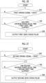
- the second shift time derivation processing is executed at a predetermined time interval during the drawing of the image by the image drawing system 10.
- This time interval may be, for example, a time interval corresponding to one cycle of the second driving signal, a time interval corresponding to a plurality of cycles, or a preset time interval regardless of the cycle.
- step S20 in Fig. 19 for each cycle, the second derivation portion 63B acquires the second phase delay time from the point in time when the second driving signal is zero to the point in time when the second angle detection signal S2c is zero in the corresponding cycle.
- step S22 the second derivation portion 63B derives the second average phase delay time by averaging the second phase delay time in the most recent plurality of cycles acquired in step S20.
- first zero cross pulse generation processing is executed during the drawing of the image by the image drawing system 10.
- step S30 in Fig. 20 the first zero cross pulse output portion 65A determines whether or not the first driving signal is zero. In a case where this determination results in a positive determination, the processing transitions to step S32. In a case where a negative determination is made, step S30 is executed again.
- step S32 the first zero cross pulse output portion 65A waits for the elapse of the added time of the first average phase delay time and the first shift time t3 1 derived by the first shift time derivation processing from the timing at which the first driving signal is zero in step S30.
- the determination in step S32 results in a positive determination, and the processing transitions to step S34.
- step S34 the first zero cross pulse output portion 65A generates the first zero cross pulse ZC1 and outputs the generated first zero cross pulse ZC1 to the light source driving portion 66.
- the processing in step S34 returns to step S30.
- the first zero cross pulse generation processing is finished.
- the second zero cross pulse generation processing is executed during the drawing of the image by the image drawing system 10.
- step S40 in Fig. 21 the second zero cross pulse output portion 65B determines whether or not the second driving signal is zero. In a case where this determination results in a positive determination, the processing transitions to step S42. In a case where a negative determination is made, step S40 is executed again.
- step S42 the second zero cross pulse output portion 65B waits for the elapse of the added time of the second average phase delay time and the second shift time t3 2 derived by the second shift time derivation processing from the timing at which the second driving signal is zero in step S40.
- the determination in step S42 results in a positive determination, and the processing transitions to step S44.
- step S44 the second zero cross pulse output portion 65B generates the second zero cross pulse ZC2 and outputs the generated second zero cross pulse ZC2 to the light source driving portion 66.
- the processing in step S44 is finished, the processing returns to step S40.
- the drawing processing of the image by the image drawing system 10 is finished, the second zero cross pulse generation processing is finished.
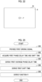
- Fig. 22 is a diagram for describing an arrangement position of the photodetector 7 in the calibration.
- the photodetector 7 is provided at a position at which the reflected light from the mirror portion 20 can be received.
- one photodetector 7 is provided at a center of a region (hereinafter, referred to as a "drawing region") R1 in which the image is drawn by the reflected light from the mirror portion 20.
- the photodetector 7 In a state where the mirror portion 20 is at a standstill, that is, in a case where the angle of the mirror portion 20 around the first axis a 1 and the angle of the mirror portion 20 around the second axis a 2 are zero, the photodetector 7 is irradiated with the light beam L reflected from the mirror portion 20. In this case, the photodetector 7 outputs a signal (hereinafter, referred to as an "irradiation signal”) representing that the irradiation is performed with the light beam L to the driving controller 5.
- irradiation signal a signal representing that the irradiation is performed with the light beam L to the driving controller 5.
- the optical scanning device 2 has a shift time derivation mode in which the first shift time t3 1 and the second shift time t3 2 are derived.
- First calibration processing shown in Fig. 23 and second calibration processing shown in Fig. 25 are executed by executing the shift time derivation mode in the calibration.
- Examples of an execution timing of the calibration include when the optical scanning device 2 is started, and a timing at which an instruction to execute the calibration is input by a user.
- the execution timing of the calibration may be before the optical scanning device 2 is shipped from a factory. In this case, for example, data obtained by the calibration is stored in a non-volatile storage portion comprised in the driving controller 5.
- the photodetector 7 may not be included in the image drawing system 10 in a user location that is a shipment destination of the optical scanning device 2.
- the reflecting surface 20A of the mirror portion 20 is continuously irradiated with the light beam L from the light source 3.
- step S50 in Fig. 23 the first driving signal generation portion 60A generates the first driving signal and provides the generated first driving signal to the pair of first actuators 31 through the first phase shift portion 62A. That is, in the first calibration processing, the mirror portion 20 is caused to swing around only the first axis a 1 and not swing around the second axis a 2 .
- step S52 for each cycle, the first derivation portion 63A acquires the first phase delay time from the point in time when the first driving signal is zero to the point in time when the first angle detection signal S1c is zero in the corresponding cycle.
- the first derivation portion 63A also acquires a shift time t4 from the point in time when the first angle detection signal S1c is zero to a point in time when the irradiation signal is input from the photodetector 7.
- the point in time when the irradiation signal is input represents a point in time when the output signal of the photodetector 7 represents that the angle of the mirror portion 20 around the first axis a 1 is zero.
- step S54 the first derivation portion 63A derives the first average phase delay time by averaging the first phase delay time in the most recent plurality of cycles acquired in step S52.
- step S56 the first derivation portion 63A derives the first shift time t3 1 by averaging the shift time t4 in the most recent plurality of cycles acquired in step S52.
- step S50 to step S56 is executed a plurality of times while the first driving frequency is changed.
- the first average phase delay time and the first shift time t3 1 also have different values. That is, since a plurality of combinations of the first average phase delay time and the first shift time t3 1 are obtained, a relationship between the first average phase delay time and the first shift time t3 1 shown in Fig. 14 as an example is obtained.
- step S58 the third derivation portion 64 derives the function f1 by approximating the obtained relationship between the first average phase delay time and the first shift time t3 1 .
- the function f1 is used in step S14 of the first shift time derivation processing (see Fig. 18 ).
- the third derivation portion 64 may store the obtained relationship between the first average phase delay time and the first shift time t3 1 as a look-up table. In a case where the processing in step S58 is finished, the first calibration processing is finished.
- step S70 in Fig. 25 the second driving signal generation portion 60B generates the second driving signal and provides the generated second driving signal to the pair of second actuators 32 through the second phase shift portion 62B. That is, in the second calibration processing, the mirror portion 20 is caused to swing around only the second axis a 2 and not swing around the first axis a 1 .
- step S72 for each cycle, the second derivation portion 63B acquires the second phase delay time from the point in time when the second driving signal is zero to the point in time when the second angle detection signal S2c is zero in the corresponding cycle.
- the second derivation portion 63B also acquires a shift time t5 from the point in time when the second angle detection signal S2c is zero to the point in time when the irradiation signal is input from the photodetector 7.
- the point in time when the irradiation signal is input represents a point in time when the output signal of the photodetector 7 represents that the angle of the mirror portion 20 around the second axis a 2 is zero.
- step S74 the second derivation portion 63B derives the second average phase delay time by averaging the second phase delay time in the most recent plurality of cycles acquired in step S72.
- step S76 the second derivation portion 63B derives the second shift time t3 2 by averaging the shift time t5 in the most recent plurality of cycles acquired in step S72.
- step S70 to step S76 is executed a plurality of times while the second driving frequency is changed.
- the second average phase delay time and the second shift time t3 2 also have different values. That is, since a plurality of combinations of the second average phase delay time and the second shift time t3 2 are obtained, a relationship between the second average phase delay time and the second shift time t3 2 shown in Fig. 15 as an example is obtained.
- step S78 the third derivation portion 64 derives the function f2 by approximating the obtained relationship between the second average phase delay time and the second shift time t3 2 .
- the function f2 is used in step S24 of the second shift time derivation processing (see Fig. 19 ).
- the third derivation portion 64 may store the obtained relationship between the second average phase delay time and the second shift time t3 2 as a look-up table. In a case where the processing in step S78 is finished, the second calibration processing is finished.
- sensing accuracy of a timing at which the angle of the mirror portion 20 is equal to the reference angle by the optical scanning device 2 can be improved using the photodetector 7. Consequently, a decrease in image quality of the drawn image can be suppressed.
- the configuration of the MMD 4 shown in the embodiment is an example.
- the configuration of the MMD 4 can be variously modified.
- the first actuators 31 that cause the mirror portion 20 to swing around the first axis a 1 may be arranged in the second movable frame 24, and the second actuators 32 that cause the mirror portion 20 to swing around the second axis a 2 may be arranged in the first movable frame 22.
- the pair of first angle detection sensors 11A and 11B are arranged at positions that face each other with the first axis a 1 interposed therebetween is described, the present disclosure is not limited thereto.
- the pair of first angle detection sensors 11A and 11B may be arranged at positions that face each other with the second axis a 2 interposed therebetween.
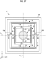
- each of the pair of first angle detection sensors 11A and 11B is arranged near the first support portions 21 on the first movable frame 22.
- the first angle detection sensor 11A is arranged near the first support portion 21 connected to one side of the mirror portion 20.
- the first angle detection sensor 11B is arranged near the first support portion 21 connected to the other side of the mirror portion 20. Accordingly, the pair of first angle detection sensors 11A and 11B are arranged at positions that face each other with the second axis a 2 interposed therebetween and face each other with the mirror portion 20 interposed therebetween. In addition, the pair of first angle detection sensors 11A and 11B are arranged at positions that are shifted in the same direction (in the example in Fig. 27 , the -X direction) from the first axis a 1 .
- the vibration noise can be removed by subtracting one of the output signals of both of the first angle detection sensors 11A and 11B from the other.
- the vibration noise can be removed by adding the output signals of both of the first angle detection sensors 11A and 11B.
- the first signal processing portion 61A includes an addition circuit 73A instead of the subtraction circuit 73.
- the addition circuit 73A outputs a value obtained by adding the signal S1b 1 input from the first angle detection sensor 11A through the buffer amplifier 71 to the signal S1b 2 input from the first angle detection sensor 11B through the variable gain amplifier 72.
- the pair of second angle detection sensors 12A and 12B may be arranged at positions that face each other with the second axis a 1 interposed therebetween.
- each of the pair of second angle detection sensors 12A and 12B is arranged near the second support portions 23 on the second movable frame 24.
- the second angle detection sensor 12A is arranged near the second support portion 23 connected to one side of the first movable frame 22.
- the second angle detection sensor 12B is arranged near the second support portion 23 connected to the other side of the first movable frame 22. Accordingly, the pair of second angle detection sensors 12A and 12B are arranged at positions that face each other with the first axis a 1 interposed therebetween and face each other with the mirror portion 20 and the first movable frame 22 interposed therebetween. In addition, the pair of second angle detection sensors 12A and 12B are arranged at positions that are shifted in the same direction (in the example in Fig. 27 , the +Y direction) from the second axis a 2 .
- the vibration noise can be removed by subtracting one of the output signals of both of the second angle detection sensors 12A and 12B from the other.
- the vibration noise can be removed by adding the output signals of both of the second angle detection sensors 12A and 12B.
- a configuration of the second signal processing portion 61B in this form example can be implemented by the same configuration as the first signal processing portion 61A shown in Fig. 28 and thus, will not be described.
- a form of providing any one of the pair of first angle detection sensors 11A and 11B in the MMD 4 may be applied.
- a form of providing any one of the pair of second angle detection sensors 12A and 12B in the MMD 4 may be applied.
- the shift times t4 and t5 are derived based on distances A1 to A4 from a position P (in the example in Fig. 29 , the center of the drawing region R1) irradiated with the light beam L reflected from the mirror portion 20 to the photodetectors 7 in a state where the mirror portion 20 is at a standstill, and an input timing of the irradiation signal from the photodetector 7.
- the first derivation portion 63A derives a point in time T1 when the angle of the mirror portion 20 around the first axis a 1 is zero, based on a ratio of the distances A1 and A2 from the position P to each photodetector 7 on the axis a 4 and a point in time when the irradiation signal is input from each photodetector 7 on the axis a 4 .
- the distance A1 is equal to the distance A2.
- the point in time T1 is a center point in time between the points in time when the irradiation signal is input from each photodetector 7 on the axis a 4 .
- the first derivation portion 63A uses a time from the point in time when the first angle detection signal S1c is zero to the derived point in time T1 as the shift time t4.
- the point in time T1 represents a point in time when the output signal of the photodetector 7 represents that the angle of the mirror portion 20 around the first axis a 1 is zero.
- the second derivation portion 63B derives a point in time T2 when the angle of the mirror portion 20 around the second axis a 2 is zero, based on a ratio of the distances A3 and A4 from the position P to each photodetector 7 on the axis a 3 and a point in time when the irradiation signal is input from each photodetector 7 on the axis a 3 .
- the distance A3 is equal to the distance A4.
- the point in time T2 is a center point in time between the points in time when the irradiation signal is input from each photodetector 7 on the axis a 3 .
- the second derivation portion 63B uses a time from the point in time when the second angle detection signal S2c is zero to the derived point in time T2 as the shift time t5.
- the point in time T2 represents a point in time when the output signal of the photodetector 7 represents that the angle of the mirror portion 20 around the second axis a 2 is zero.
- the mirror portion 20 may be capable of reflecting the light beam L in a wider region than the drawing region R1 based on the drawing data. That is, as specifications of the device, the mirror portion 20 may be capable of drawing the image in a state where the first deflection angle ⁇ 1 and the second deflection angle ⁇ 2 are set to be larger than when the image is drawn in the drawing region R1 based on the drawing data.
- one photodetector 7 may be provided in each end part on the axis as and each end part on the axis a 4 in a drawable region R2 outside the drawing region R1.
- one photodetector 7 may be provided at each of two points other than each end part on the axis as corresponding to the first axis a 1 and each of two points other than each end part on the axis a 4 corresponding to the second axis a 2 in the drawable region.
- FIG. 33 an example of applying the drawing region R1 as the drawable region is shown.
- the first derivation portion 63A can derive the point in time T1 when the angle of the mirror portion 20 around the first axis a 1 is zero, based on the ratio of the distances A1 and A2 from the position P to each photodetector 7 on the axis a 4 and the point in time when the irradiation signal is input from each photodetector 7 on the axis a 4 .
- the second derivation portion 63B can derive the point in time T2 when the angle of the mirror portion 20 around the second axis a 2 is zero, based on the ratio of the distances A3 and A4 from the position P to each photodetector 7 on the axis as and the point in time when the irradiation signal is input from each photodetector 7 on the axis as.
- the photodetector 7 may be in a non-driven state during the drawing of the image. In this case, power supply to the photodetector 7 can be stopped. Consequently, power consumption can be reduced.
- the present disclosure is not limited thereto.
- a form of acquiring the first average phase delay time and the second average phase delay time by executing an average phase delay time derivation mode in which the first average phase delay time and the second average phase delay time are derived in the calibration may be applied.
- the first average phase delay time and the second average phase delay time acquired in advance in the calibration are used in the generation of the first zero cross pulse ZC1 and the second zero cross pulse ZC2.
- Examples of the execution timing of the calibration in this case include when the MMD 4 is started, and the timing at which the instruction to execute the calibration is input by the user.
- Fig. 34 shows an example of the relationship between the first average phase delay time and the first shift time t3 1 in a case where a driving voltage V1 of the first driving signal is differently set.
- the driving voltage V1 of the first driving signal corresponds to an amplitude of the first driving signal.
- a solid line in Fig. 34 shows a case where the driving voltage V1 is higher than a broken line.
- the first shift time t3 1 is increased.
- the first shift time t3 1 changes in accordance with not only the driving voltage V1 of the first driving signal but also the first driving frequency.
- the third derivation portion 64 may further derive the first shift time t3 1 corresponding to a first driving frequency F1 and a driving voltage V1 of the first driving signal in accordance with a function f3 shown as follows.
- t3 1 f3 t1 avg , F1 , V1
- the third derivation portion 64 may further derive the second shift time t3 2 corresponding to a second driving frequency F2 and a driving voltage V2 of the second driving signal in accordance with a function f4 shown as follows.
- t3 2 f4 t2 avg , F2 , V2
- the third derivation portion 64 may further derive the first shift time t3 1 and the second shift time t3 2 corresponding to an ambient temperature T in accordance with functions f5 and f6 shown as follows.
- a temperature sensor that measures the ambient temperature is provided in the MMD 4.
- t3 1 f5 t1 avg
- T t3 2 f6 t2 avg
- the third derivation portion 64 may further derive the first shift time t3 1 corresponding to the first driving frequency F1, the driving voltage V1 of the first driving signal, and the ambient temperature T in accordance with a function f7 shown as follows.
- t 3 1 f 7 t1 avg , F1 , V1 , T
- the driving controller 5 can be configured using at least one of an analog operation circuit or a digital operation circuit.
- the driving controller 5 may be configured with one processor or may be configured with a combination of two or more processors of the same type or different types.
- Examples of the processor include a central processing unit (CPU), a programmable logic device (PLD), and a dedicated electric circuit.
- the CPU is a general-purpose processor that executes software (program) to function as various processing portions.
- the PLD is a processor such as a field programmable gate array (FPGA) that has a circuit configuration changeable after manufacturing.
- the dedicated electric circuit is a processor such as an application specific integrated circuit (ASIC) that has a circuit configuration dedicatedly designed to perform specific processing.
- ASIC application specific integrated circuit
Landscapes
- Physics & Mathematics (AREA)
- Optics & Photonics (AREA)
- General Physics & Mathematics (AREA)
- Engineering & Computer Science (AREA)
- Multimedia (AREA)
- Signal Processing (AREA)
- Mechanical Optical Scanning Systems (AREA)
Claims (18)
- Optische Abtastvorrichtung (2), umfassend:einen Spiegelabschnitt (20) mit einer reflektierenden Oberfläche (20A), auf der ein einfallender Strahl reflektiert wird;ein erstes Stellglied (31), das bewirkt, dass der Spiegelabschnitt (20) um eine erste Achse (a1) schwenkt, die in einer Ebene ist, welche die reflektierende Oberfläche (20A) zu einer Zeit eines Stillstands des Spiegelabschnittes (20) beinhaltet;ein zweites Stellglied (32), das bewirkt, dass der Spiegelabschnitt (20) um eine zweite Achse (a2) schwenkt, die in der Ebene ist, welche die reflektierende Oberfläche (20A) zu der Zeit des Stillstands des Spiegelabschnittes (20) beinhaltet und die erste Achse (a1) schneidet;einen ersten Winkelerkennungssensor, der ein Signal ausgibt, das einem Winkel des Spiegelabschnittes (20) um die erste Achse (a1) entspricht;einen zweiten Winkelerkennungssensor, der ein Signal ausgibt, das einem Winkel des Spiegelabschnittes (20) um die zweite Achse (a2) entspricht;zumindest einen Photodetektor (7), der an einer Position bereitgestellt ist, an der reflektiertes Licht von dem Spiegelabschnitt (20) empfangbar ist; undzumindest einen Prozessor, der konfiguriert ist, um eine Zeitsteuerung eines ersten Referenzsignals zu erzeugen, das repräsentiert, dass der Winkel des Spiegelabschnittes (20) um die erste Achse (a1) gleich einem ersten Referenzwinkel ist, und um eine Zeitsteuerung eines zweiten Referenzsignals zu erzeugen, das repräsentiert, dass der Winkel des Spiegelabschnittes (20) um die zweite Achse (a2) gleich einem zweiten Referenzwinkel ist,wobei der Prozessor konfiguriert ist zumBereitstellen eines ersten Antriebssignals mit einer ersten Antriebsfrequenz für das erste Stellglied (31),Bereitstellen eines zweiten Antriebssignals mit einer zweiten Antriebsfrequenz für das zweite Stellglied (32),Ableiten einer ersten durchschnittlichen Phasenverzögerungszeit durch Mitteln einer ersten Phasenverzögerungszeit des Ausgangssignals des ersten Winkelerkennungssensors in Bezug auf das erste Antriebssignal in einer Vielzahl von Zyklen, undAbleiten einer zweiten durchschnittlichen Phasenverzögerungszeit durch Mitteln einer zweiten Phasenverzögerungszeit des Ausgangssignals des zweiten Winkelerkennungssensors in Bezug auf das zweite Antriebssignal in einer Vielzahl von Zyklen,Ableiten einer ersten Verschiebungszeit, die eine Verschiebungszeit ist, die zum Korrigieren einer Erzeugungszeitsteuerung eines ersten Referenzsignals verwendet wird, das repräsentiert, dass der Winkel des Spiegelabschnittes (20) um die erste Achse (a1) gleich einem ersten Referenzwinkel ist, und eine Verschiebungszeit eines Zeitpunktes ist, zu dem der Winkel des Spiegelabschnittes (20) um die erste Achse (a1) gleich dem ersten Referenzwinkel in Bezug auf einen Zeitpunkt ist, zu dem das Ausgangssignal des ersten Winkelerkennungssensors repräsentiert, dass der Winkel des Spiegelabschnittes (20) um die erste Achse (a1) gleich dem ersten Referenzwinkel ist, basierend auf einem Ausgangssignal des Photodetektors (7), wobei der Zeitpunkt, zu dem das Ausgangssignal des ersten Winkelerkennungssensors repräsentiert, dass der Winkel des Spiegelabschnittes (20) um die erste Achse (a1) gleich dem ersten Referenzwinkel ist, ein Zeitpunkt nach einem Verstreichen der ersten durchschnittlichen Phasenverzögerungszeit von einem Zeitpunkt ist, zu dem das erste Antriebssignal repräsentiert, dass der Winkel des Spiegelabschnittes (20) um die erste Achse (a1) gleich dem ersten Referenzwinkel ist, undAbleiten einer zweiten Verschiebungszeit, die eine Verschiebungszeit ist, die zum Korrigieren einer Erzeugungszeitsteuerung eines zweiten Referenzsignals verwendet wird, das repräsentiert, dass der Winkel des Spiegelabschnittes (20) um die zweite Achse (a2) gleich einem zweiten Referenzwinkel ist, und eine Verschiebungszeit eines Zeitpunktes ist, zu dem der Winkel des Spiegelabschnittes (20) um die zweite Achse (a2) gleich dem zweiten Referenzwinkel in Bezug auf einen Zeitpunkt ist, zu dem das Ausgangssignal des zweiten Winkelerkennungssensors repräsentiert, dass der Winkel des Spiegelabschnittes (20) um die zweite Achse (a2) gleich dem zweiten Referenzwinkel ist, basierend auf dem Ausgangssignal des Photodetektors (7), wobei der Zeitpunkt, zu dem das Ausgangssignal des zweiten Winkelerkennungssensors repräsentiert, dass der Winkel des Spiegelabschnittes (20) um die zweite Achse (a2) gleich dem zweiten Referenzwinkel ist, ein Zeitpunkt nach einem Verstreichen der zweiten durchschnittlichen Phasenverzögerungszeit von einem Zeitpunkt ist, zu dem das zweite Antriebssignal repräsentiert, dass der Winkel des Spiegelabschnittes (20) um die zweite Achse (a2) gleich dem zweiten Referenzwinkel ist.
- Optische Abtastvorrichtung (2) nach Anspruch 1,
wobei ein Photodetektor (7) in einer Mitte eines Bereichs bereitgestellt ist, in dem ein Bild durch das reflektierte Licht von dem Spiegelabschnitt (20) gezeichnet wird. - Optische Abtastvorrichtung (2) nach Anspruch 1,
wobei der Photodetektor (7) an einer Achse, die der ersten Achse (a1) entspricht, und an einer Achse, die der zweiten Achse (a2) entspricht, in einem Bereich, in dem ein Bild durch das reflektierte Licht von dem Spiegelabschnitt (20) gezeichnet werden kann, bereitgestellt ist. - Optische Abtastvorrichtung (2) nach Anspruch 3,
wobei zumindest ein Photodetektor (7) in jedem Endteil auf der Achse, die der ersten Achse (a1) entspricht, und jedem Endteil auf der Achse, die der zweiten Achse (a2) entspricht, in dem Bereich, in dem das Bild durch das reflektierte Licht von dem Spiegelabschnitt (20) gezeichnet werden kann, bereitgestellt ist. - Optische Abtastvorrichtung (2) nach Anspruch 1,wobei der Prozessor konfiguriert ist zumAbleiten der ersten durchschnittlichen Phasenverzögerungszeit durch Mitteln der ersten Phasenverzögerungszeit zu einem Zeitpunkt, zu dem das Ausgangssignal des ersten Winkelerkennungssensors null ist, undAbleiten der zweiten durchschnittlichen Phasenverzögerungszeit durch Mitteln der zweiten Phasenverzögerungszeit zu einem Zeitpunkt, zu dem das Ausgangssignal des zweiten Winkelerkennungssensors null ist.
- Optische Abtastvorrichtung (2) nach Anspruch 5,wobei der Prozessor konfiguriert ist zumAbleiten der ersten durchschnittlichen Phasenverzögerungszeit durch Mitteln der ersten Phasenverzögerungszeit von einem Zeitpunkt, zu dem das erste Antriebssignal null ist, zu dem Zeitpunkt, zu dem das Ausgangssignal des ersten Winkelerkennungssensors null ist, in einem entsprechenden Zyklus, undAbleiten der zweiten durchschnittlichen Phasenverzögerungszeit durch Mitteln der zweiten Phasenverzögerungszeit von einem Zeitpunkt, zu dem das zweite Antriebssignal null ist, zu dem Zeitpunkt, zu dem das Ausgangssignal des zweiten Winkelerkennungssensors null ist, in einem entsprechenden Zyklus.
- Optische Abtastvorrichtung (2) nach einem der Ansprüche 1 bis 6,wobei der erste Referenzwinkel und der zweite Referenzwinkel null sind,die erste Verschiebungszeit eine Zeit ist von einem Zeitpunkt, zu dem das Ausgangssignal des ersten Winkelerkennungssensors repräsentiert, dass der Winkel des Spiegelabschnittes (20) um die erste Achse (a1) null ist, zu einem Zeitpunkt, zu dem das Ausgangssignal des Photodetektors (7) repräsentiert, dass der Winkel des Spiegelabschnittes (20) um die erste Achse (a1) null ist, unddie zweite Verschiebungszeit eine Zeit ist von einem Zeitpunkt, zu dem das Ausgangssignal des zweiten Winkelerkennungssensors repräsentiert, dass der Winkel des Spiegelabschnittes (20) um die zweite Achse (a2) null ist, zu einem Zeitpunkt, zu dem das Ausgangssignal des Photodetektors (7) repräsentiert, dass der Winkel des Spiegelabschnittes (20) um die zweite Achse (a2) null ist.
- Optische Abtastvorrichtung (2) nach einem der Ansprüche 1 bis 7,wobei der Prozessor konfiguriert ist zumErzeugen des ersten Referenzsignals zu einem Zeitpunkt nach einem Ablauf der ersten Verschiebungszeit von dem Zeitpunkt, zu dem das Ausgangssignal des ersten Winkelerkennungssensors repräsentiert, dass der Winkel des Spiegelabschnittes (20) um die erste Achse (a1) gleich dem ersten Referenzwinkel ist, undErzeugen des zweiten Referenzsignals zu einem Zeitpunkt nach einem Ablauf der zweiten Verschiebungszeit von dem Zeitpunkt, zu dem das Ausgangssignal des zweiten Winkelerkennungssensors repräsentiert, dass der Winkel des Spiegelabschnittes (20) um die zweite Achse (a2) gleich dem zweiten Referenzwinkel ist.
- Optische Abtastvorrichtung (2) nach Anspruch 8,wobei ein Verschiebungszeitableitungsmodus, in dem die erste Verschiebungszeit und die zweite Verschiebungszeit abgeleitet werden, bereitgestellt ist, undder Prozessor konfiguriert ist zumErfassen der ersten Verschiebungszeit und der zweiten Verschiebungszeit für jede voreingestellte Bedingung durch Ausführen des Verschiebungszeitableitungsmodus bei Kalibrierung, undVerwenden der ersten Verschiebungszeit und der zweiten Verschiebungszeit, die im Voraus bei der Kalibrierung erfasst werden, bei dem Erzeugen des ersten Referenzsignals und des zweiten Referenzsignals.
- Optische Abtastvorrichtung (2) nach Anspruch 9,
wobei die Bedingung die erste Phasenverzögerungszeit und die zweite Phasenverzögerungszeit beinhaltet. - Optische Abtastvorrichtung (2) nach Anspruch 10,
wobei die Bedingung ferner eine Antriebsspannung des ersten Antriebssignals und eine Antriebsspannung des zweiten Antriebssignals beinhaltet. - Optische Abtastvorrichtung (2) nach Anspruch 10 oder 11,
wobei die Bedingung ferner die erste Antriebsfrequenz und die zweite Antriebsfrequenz beinhaltet. - Optische Abtastvorrichtung (2) nach einem der Ansprüche 10 bis 12,
wobei die Bedingung ferner eine Umgebungstemperatur beinhaltet. - Optische Abtastvorrichtung (2) nach einem der Ansprüche 1 bis 13,
wobei der Photodetektor (7) eine Photodiode ist. - Optische Abtastvorrichtung (2) nach einem der Ansprüche 1 bis 14,
wobei der Photodetektor (7) während des Zeichnens eines Bildes in einem nicht angetriebenen Zustand ist. - Optische Abtastvorrichtung (2) nach einem der Ansprüche 1 bis 15,wobei der erste Winkelerkennungssensor ein Paar von Winkelerkennungssensoren (11A, 11B) beinhaltet, die an Positionen angeordnet sind, die einander zugewandt sind, wobei die erste Achse (a1) oder die zweite Achse (a2) zwischen den Positionen liegt,das Ausgangssignal des ersten Winkelerkennungssensors ein Ausgangssignal ist, das durch Addieren oder Subtrahieren eines Paares von Ausgangssignalen erhalten wird, die von dem Paar von Winkelerkennungssensoren (11A, 11B) ausgegeben werden,der zweite Winkelerkennungssensor ein Paar von Winkelerkennungssensoren (12A, 12B) beinhaltet, die an Positionen angeordnet sind, die einander zugewandt sind, wobei die erste Achse (a1) oder die zweite Achse (a2) zwischen den Positionen liegt, unddas Ausgangssignal des zweiten Winkelerkennungssensors ein Ausgangssignal ist, das durch Addieren oder Subtrahieren eines Paares von Ausgangssignalen erhalten wird, die von dem Paar von Winkelerkennungssensoren (12A, 12B) ausgegeben werden.
- Bildzeichnungssystem (10), umfassend:die optische Abtastvorrichtung (2) nach einem der Ansprüche 1 bis 16; undeine Lichtquelle (3), die den Spiegelabschnitt (20) mit Licht bestrahlt.
- Antriebsverfahren einer optischen Abtastvorrichtung (2), die einen Spiegelabschnitt (20) mit einer reflektierenden Oberfläche (20A), auf der ein einfallender Strahl reflektiert wird, ein erstes Stellglied (31), das bewirkt, dass der Spiegelabschnitt (20) um eine erste Achse (a1) schwingt, die in einer Ebene ist, welche die reflektierende Oberfläche (20A) zu einer Zeit eines Stillstands des Spiegelabschnittes (20) beinhaltet, ein zweites Stellglied (32), das bewirkt, dass der Spiegelabschnitt (20) um eine zweite Achse (a2) schwingt, die in der Ebene ist, welche die reflektierende Oberfläche (20A) zu dem Zeit des Stillstands des Spiegelabschnittes (20) beinhaltet und die erste Achse (a1) schneidet, einen ersten Winkelerkennungssensor, der ein Signal ausgibt, das einem Winkel des Spiegelabschnittes (20) um die erste Achse (a1) entspricht, einen zweiten Winkelerkennungssensor, der ein Signal ausgibt, das einem Winkel des Spiegelabschnittes (20) um die zweite Achse (a2) entspricht, und zumindest einen Photodetektor (7), der an einer Position bereitgestellt ist, an der reflektiertes Licht von dem Spiegelabschnitt (20) empfangbar ist, beinhaltet, wobei das Antriebsverfahren Folgendes umfasst:Bereitstellen eines ersten Antriebssignals mit einer ersten Antriebsfrequenz für das erste Stellglied (31);Bereitstellen eines zweiten Antriebssignals mit einer zweiten Antriebsfrequenz für das zweite Stellglied (32);Ableiten einer ersten durchschnittlichen Phasenverzögerungszeit durch Mitteln einer ersten Phasenverzögerungszeit des Ausgangssignals des ersten Winkelerkennungssensors in Bezug auf das erste Antriebssignal in einer Vielzahl von Zyklen; undAbleiten einer zweiten durchschnittlichen Phasenverzögerungszeit durch Mitteln einer zweiten Phasenverzögerungszeit des Ausgangssignals des zweiten Winkelerkennungssensors in Bezug auf das zweite Antriebssignal in einer Vielzahl von Zyklen;Erzeugen einer Zeitsteuerung eines ersten Referenzsignals, das repräsentiert, dass der Winkel des Spiegelabschnittes (20) um die erste Achse (a1) gleich einem ersten Referenzwinkel ist, und Erzeugen einer Zeitsteuerung eines zweiten Referenzsignals, das repräsentiert, dass der Winkel des Spiegelabschnittes (20) um die zweite Achse (a2) gleich einem zweiten Referenzwinkel ist;Ableiten einer ersten Verschiebungszeit, die eine Verschiebungszeit ist, die zum Korrigieren der Erzeugungszeitsteuerung des ersten Referenzsignals verwendet wird, und eine Verschiebungszeit eines Zeitpunktes ist, zu dem der Winkel des Spiegelabschnittes (20) um die erste Achse (a1) gleich dem ersten Referenzwinkel in Bezug auf einen Zeitpunkt ist, zu dem das Ausgangssignal des ersten Winkelerkennungssensors repräsentiert, dass der Winkel des Spiegelabschnittes (20) um die erste Achse (a1) gleich dem ersten Referenzwinkel ist, basierend auf einem Ausgangssignal des Photodetektors (7), wobei der Zeitpunkt, zu dem das Ausgangssignal des ersten Winkelerkennungssensors repräsentiert, dass der Winkel des Spiegelabschnittes (20) um die erste Achse (a1) gleich dem ersten Referenzwinkel ist, ein Zeitpunkt nach einem Verstreichen der ersten durchschnittlichen Phasenverzögerungszeit von einem Zeitpunkt ist, zu dem das erste Antriebssignal repräsentiert, dass der Winkel des Spiegelabschnittes (20) um die erste Achse (a1) gleich dem ersten Referenzwinkel ist; undAbleiten einer zweiten Verschiebungszeit, die eine Verschiebungszeit ist, die zum Korrigieren der Erzeugungszeitsteuerung eines zweiten Referenzsignals verwendet wird, und eine Verschiebungszeit eines Zeitpunkts ist, zu dem der Winkel des Spiegelabschnittes (20) um die zweite Achse (a2) gleich dem zweiten Referenzwinkel in Bezug auf einen Zeitpunkt ist, zu dem das Ausgangssignal des zweiten Winkelerkennungssensors repräsentiert, dass der Winkel des Spiegelabschnittes (20) um die zweite Achse (a2) gleich dem zweiten Referenzwinkel ist, basierend auf dem Ausgangssignal des Photodetektors (7), wobei der Zeitpunkt, zu dem das Ausgangssignal des zweiten Winkelerkennungssensors repräsentiert, dass der Winkel des Spiegelabschnittes (20) um die zweite Achse (a2) gleich dem zweiten Referenzwinkel ist, ein Zeitpunkt nach einem Ablauf der zweiten durchschnittlichen Phasenverzögerungszeit von einem Zeitpunkt ist, zu dem das zweite Antriebssignal repräsentiert, dass der Winkel des Spiegelabschnittes (20) um die zweite Achse (a2) gleich dem zweiten Referenzwinkel ist.
Applications Claiming Priority (1)
| Application Number | Priority Date | Filing Date | Title |
|---|---|---|---|
| JP2021101749A JP7601720B2 (ja) | 2021-06-18 | 2021-06-18 | 光走査装置、光走査装置の駆動方法、及び画像描画システム |
Publications (2)
| Publication Number | Publication Date |
|---|---|
| EP4105709A1 EP4105709A1 (de) | 2022-12-21 |
| EP4105709B1 true EP4105709B1 (de) | 2024-12-11 |
Family
ID=81653479
Family Applications (1)
| Application Number | Title | Priority Date | Filing Date |
|---|---|---|---|
| EP22173297.7A Active EP4105709B1 (de) | 2021-06-18 | 2022-05-13 | Optische abtastvorrichtung, antriebsverfahren einer optischen abtastvorrichtung und bildzeichnungssystem |
Country Status (4)
| Country | Link |
|---|---|
| US (1) | US12282155B2 (de) |
| EP (1) | EP4105709B1 (de) |
| JP (1) | JP7601720B2 (de) |
| CN (1) | CN115494635A (de) |
Families Citing this family (4)
| Publication number | Priority date | Publication date | Assignee | Title |
|---|---|---|---|---|
| JP7481099B2 (ja) * | 2019-09-11 | 2024-05-10 | 浜松ホトニクス株式会社 | 光走査システムの製造方法、光走査装置の製造方法及びデータ取得方法 |
| JP7612521B2 (ja) * | 2021-06-01 | 2025-01-14 | 富士フイルム株式会社 | 光走査装置、光走査装置の駆動方法、及び画像描画システム |
| JP7770970B2 (ja) * | 2022-03-25 | 2025-11-17 | 富士フイルム株式会社 | 光走査装置、光走査装置の駆動方法、及び画像描画システム |
| CN121002420A (zh) * | 2023-03-27 | 2025-11-21 | 富士胶片株式会社 | 光学扫描装置、图像绘制系统及反射镜装置的驱动方法 |
Family Cites Families (11)
| Publication number | Priority date | Publication date | Assignee | Title |
|---|---|---|---|---|
| TWI226940B (en) | 2002-10-01 | 2005-01-21 | Sony Corp | Optical scan device, image position calibration method, and image display device |
| KR100682955B1 (ko) | 2006-01-06 | 2007-02-15 | 삼성전자주식회사 | 스캐너의 구동특성 평가장치 및 방법 |
| JP2010079198A (ja) | 2008-09-29 | 2010-04-08 | Brother Ind Ltd | 画像投影装置 |
| JP5375309B2 (ja) | 2009-04-28 | 2013-12-25 | リコーイメージング株式会社 | マイクロミラー装置 |
| JP2012063413A (ja) | 2010-09-14 | 2012-03-29 | Ricoh Co Ltd | 光走査装置およびこの光走査装置を組み込んだ画像形成装置ならびに投影装置 |
| DE112013006119B4 (de) | 2012-12-21 | 2021-03-18 | Mitsubishi Electric Corp. | Optische Abtasteinrichtung und Projektor |
| US9693029B1 (en) | 2015-12-22 | 2017-06-27 | Microvision, Inc. | System and method for feedback control in scanning projectors |
| JP6978659B2 (ja) * | 2016-12-21 | 2021-12-08 | ミツミ電機株式会社 | 画像投影装置および補償方法 |
| JP2020016720A (ja) * | 2018-07-24 | 2020-01-30 | スタンレー電気株式会社 | 光走査装置 |
| US10939080B2 (en) * | 2019-03-29 | 2021-03-02 | Facebook Technologies, Llc | Trajectory estimation for a MEMS reflector |
| JP2021033011A (ja) * | 2019-08-22 | 2021-03-01 | パイオニア株式会社 | 光走査装置、光走査方法およびプログラム |
-
2021
- 2021-06-18 JP JP2021101749A patent/JP7601720B2/ja active Active
-
2022
- 2022-05-06 US US17/738,788 patent/US12282155B2/en active Active
- 2022-05-13 EP EP22173297.7A patent/EP4105709B1/de active Active
- 2022-05-20 CN CN202210550007.5A patent/CN115494635A/zh active Pending
Also Published As
| Publication number | Publication date |
|---|---|
| JP2023000751A (ja) | 2023-01-04 |
| CN115494635A (zh) | 2022-12-20 |
| US12282155B2 (en) | 2025-04-22 |
| JP7601720B2 (ja) | 2024-12-17 |
| US20220404613A1 (en) | 2022-12-22 |
| EP4105709A1 (de) | 2022-12-21 |
Similar Documents
| Publication | Publication Date | Title |
|---|---|---|
| EP4105709B1 (de) | Optische abtastvorrichtung, antriebsverfahren einer optischen abtastvorrichtung und bildzeichnungssystem | |
| US12320971B2 (en) | Optical scanning device, driving method of optical scanning device, and image drawing system | |
| US7821694B2 (en) | Optical scan device, image display device, method of modifying resonance frequency of optical scanner, and method of correcting position of reflection mirror | |
| JP5316346B2 (ja) | 網膜走査型画像表示装置 | |
| US20230176361A1 (en) | Optical scanning device, method of driving optical scanning device, and image drawing system | |
| WO2017183368A1 (ja) | ミラー装置、ミラーの駆動方法、光照射装置及び画像取得装置 | |
| EP4099083B1 (de) | Optische abtastvorrichtung, antriebsverfahren einer optischen abtastvorrichtung und bildzeichnungssystem | |
| JP2020106741A (ja) | 光走査装置及びその制御方法 | |
| US12401771B2 (en) | Optical scanning device, driving method of optical scanning device, and image drawing system | |
| US12422666B2 (en) | Optical scanning device, driving method of optical scanning device, and image drawing system | |
| WO2011108395A1 (ja) | 光走査装置及びそれを備えた画像表示装置 | |
| US20260009999A1 (en) | Optical scanning device, image drawing system, and driving method of mirror device | |
| JPS62237420A (ja) | ガルバノミラ−を用いた画像記録装置 | |
| JP2024115218A (ja) | 測距方法及び測距装置 | |
| JP2018536195A (ja) | 光ビームを偏向するための装置及び方法 | |
| CN121969977A (zh) | 光扫描装置及光扫描装置的驱动方法 | |
| JP2022187717A (ja) | 画像形成装置、及びその作動方法 | |
| JPH09226174A (ja) | マルチビーム走査装置 | |
| WO2017195256A1 (ja) | 光走査型観察装置および光走査型観察方法 |
Legal Events
| Date | Code | Title | Description |
|---|---|---|---|
| PUAI | Public reference made under article 153(3) epc to a published international application that has entered the european phase |
Free format text: ORIGINAL CODE: 0009012 |
|
| STAA | Information on the status of an ep patent application or granted ep patent |
Free format text: STATUS: THE APPLICATION HAS BEEN PUBLISHED |
|
| AK | Designated contracting states |
Kind code of ref document: A1 Designated state(s): AL AT BE BG CH CY CZ DE DK EE ES FI FR GB GR HR HU IE IS IT LI LT LU LV MC MK MT NL NO PL PT RO RS SE SI SK SM TR |
|
| STAA | Information on the status of an ep patent application or granted ep patent |
Free format text: STATUS: REQUEST FOR EXAMINATION WAS MADE |
|
| 17P | Request for examination filed |
Effective date: 20230426 |
|
| RBV | Designated contracting states (corrected) |
Designated state(s): AL AT BE BG CH CY CZ DE DK EE ES FI FR GB GR HR HU IE IS IT LI LT LU LV MC MK MT NL NO PL PT RO RS SE SI SK SM TR |
|
| GRAP | Despatch of communication of intention to grant a patent |
Free format text: ORIGINAL CODE: EPIDOSNIGR1 |
|
| STAA | Information on the status of an ep patent application or granted ep patent |
Free format text: STATUS: GRANT OF PATENT IS INTENDED |
|
| RIC1 | Information provided on ipc code assigned before grant |
Ipc: H04N 9/31 20060101ALI20240802BHEP Ipc: G02B 26/08 20060101ALI20240802BHEP Ipc: G02B 26/10 20060101AFI20240802BHEP |
|
| INTG | Intention to grant announced |
Effective date: 20240821 |
|
| GRAS | Grant fee paid |
Free format text: ORIGINAL CODE: EPIDOSNIGR3 |
|
| GRAA | (expected) grant |
Free format text: ORIGINAL CODE: 0009210 |
|
| STAA | Information on the status of an ep patent application or granted ep patent |
Free format text: STATUS: THE PATENT HAS BEEN GRANTED |
|
| P01 | Opt-out of the competence of the unified patent court (upc) registered |
Free format text: CASE NUMBER: APP_55537/2024 Effective date: 20241009 |
|
| AK | Designated contracting states |
Kind code of ref document: B1 Designated state(s): AL AT BE BG CH CY CZ DE DK EE ES FI FR GB GR HR HU IE IS IT LI LT LU LV MC MK MT NL NO PL PT RO RS SE SI SK SM TR |
|
| REG | Reference to a national code |
Ref country code: GB Ref legal event code: FG4D |
|
| REG | Reference to a national code |
Ref country code: CH Ref legal event code: EP |
|
| REG | Reference to a national code |
Ref country code: IE Ref legal event code: FG4D |
|
| REG | Reference to a national code |
Ref country code: DE Ref legal event code: R096 Ref document number: 602022008536 Country of ref document: DE |
|
| REG | Reference to a national code |
Ref country code: LT Ref legal event code: MG9D |
|
| PG25 | Lapsed in a contracting state [announced via postgrant information from national office to epo] |
Ref country code: HR Free format text: LAPSE BECAUSE OF FAILURE TO SUBMIT A TRANSLATION OF THE DESCRIPTION OR TO PAY THE FEE WITHIN THE PRESCRIBED TIME-LIMIT Effective date: 20241211 |
|
| PG25 | Lapsed in a contracting state [announced via postgrant information from national office to epo] |
Ref country code: FI Free format text: LAPSE BECAUSE OF FAILURE TO SUBMIT A TRANSLATION OF THE DESCRIPTION OR TO PAY THE FEE WITHIN THE PRESCRIBED TIME-LIMIT Effective date: 20241211 |
|
| PG25 | Lapsed in a contracting state [announced via postgrant information from national office to epo] |
Ref country code: BG Free format text: LAPSE BECAUSE OF FAILURE TO SUBMIT A TRANSLATION OF THE DESCRIPTION OR TO PAY THE FEE WITHIN THE PRESCRIBED TIME-LIMIT Effective date: 20241211 |
|
| REG | Reference to a national code |
Ref country code: NL Ref legal event code: MP Effective date: 20241211 |
|
| PG25 | Lapsed in a contracting state [announced via postgrant information from national office to epo] |
Ref country code: ES Free format text: LAPSE BECAUSE OF FAILURE TO SUBMIT A TRANSLATION OF THE DESCRIPTION OR TO PAY THE FEE WITHIN THE PRESCRIBED TIME-LIMIT Effective date: 20241211 |
|
| PG25 | Lapsed in a contracting state [announced via postgrant information from national office to epo] |
Ref country code: NO Free format text: LAPSE BECAUSE OF FAILURE TO SUBMIT A TRANSLATION OF THE DESCRIPTION OR TO PAY THE FEE WITHIN THE PRESCRIBED TIME-LIMIT Effective date: 20250311 |
|
| PG25 | Lapsed in a contracting state [announced via postgrant information from national office to epo] |
Ref country code: LV Free format text: LAPSE BECAUSE OF FAILURE TO SUBMIT A TRANSLATION OF THE DESCRIPTION OR TO PAY THE FEE WITHIN THE PRESCRIBED TIME-LIMIT Effective date: 20241211 Ref country code: GR Free format text: LAPSE BECAUSE OF FAILURE TO SUBMIT A TRANSLATION OF THE DESCRIPTION OR TO PAY THE FEE WITHIN THE PRESCRIBED TIME-LIMIT Effective date: 20250312 |
|
| PG25 | Lapsed in a contracting state [announced via postgrant information from national office to epo] |
Ref country code: RS Free format text: LAPSE BECAUSE OF FAILURE TO SUBMIT A TRANSLATION OF THE DESCRIPTION OR TO PAY THE FEE WITHIN THE PRESCRIBED TIME-LIMIT Effective date: 20250311 |
|
| PG25 | Lapsed in a contracting state [announced via postgrant information from national office to epo] |
Ref country code: NL Free format text: LAPSE BECAUSE OF FAILURE TO SUBMIT A TRANSLATION OF THE DESCRIPTION OR TO PAY THE FEE WITHIN THE PRESCRIBED TIME-LIMIT Effective date: 20241211 |
|
| REG | Reference to a national code |
Ref country code: AT Ref legal event code: MK05 Ref document number: 1750847 Country of ref document: AT Kind code of ref document: T Effective date: 20241211 |
|
| PG25 | Lapsed in a contracting state [announced via postgrant information from national office to epo] |
Ref country code: SM Free format text: LAPSE BECAUSE OF FAILURE TO SUBMIT A TRANSLATION OF THE DESCRIPTION OR TO PAY THE FEE WITHIN THE PRESCRIBED TIME-LIMIT Effective date: 20241211 |
|
| PG25 | Lapsed in a contracting state [announced via postgrant information from national office to epo] |
Ref country code: PL Free format text: LAPSE BECAUSE OF FAILURE TO SUBMIT A TRANSLATION OF THE DESCRIPTION OR TO PAY THE FEE WITHIN THE PRESCRIBED TIME-LIMIT Effective date: 20241211 |
|
| PGFP | Annual fee paid to national office [announced via postgrant information from national office to epo] |
Ref country code: DE Payment date: 20250402 Year of fee payment: 4 |
|
| PG25 | Lapsed in a contracting state [announced via postgrant information from national office to epo] |
Ref country code: IS Free format text: LAPSE BECAUSE OF FAILURE TO SUBMIT A TRANSLATION OF THE DESCRIPTION OR TO PAY THE FEE WITHIN THE PRESCRIBED TIME-LIMIT Effective date: 20250411 |
|
| PGFP | Annual fee paid to national office [announced via postgrant information from national office to epo] |
Ref country code: IT Payment date: 20250531 Year of fee payment: 4 |
|
| PG25 | Lapsed in a contracting state [announced via postgrant information from national office to epo] |
Ref country code: PT Free format text: LAPSE BECAUSE OF FAILURE TO SUBMIT A TRANSLATION OF THE DESCRIPTION OR TO PAY THE FEE WITHIN THE PRESCRIBED TIME-LIMIT Effective date: 20250411 |
|
| PG25 | Lapsed in a contracting state [announced via postgrant information from national office to epo] |
Ref country code: EE Free format text: LAPSE BECAUSE OF FAILURE TO SUBMIT A TRANSLATION OF THE DESCRIPTION OR TO PAY THE FEE WITHIN THE PRESCRIBED TIME-LIMIT Effective date: 20241211 |
|
| PG25 | Lapsed in a contracting state [announced via postgrant information from national office to epo] |
Ref country code: RO Free format text: LAPSE BECAUSE OF FAILURE TO SUBMIT A TRANSLATION OF THE DESCRIPTION OR TO PAY THE FEE WITHIN THE PRESCRIBED TIME-LIMIT Effective date: 20241211 Ref country code: AT Free format text: LAPSE BECAUSE OF FAILURE TO SUBMIT A TRANSLATION OF THE DESCRIPTION OR TO PAY THE FEE WITHIN THE PRESCRIBED TIME-LIMIT Effective date: 20241211 |
|
| PG25 | Lapsed in a contracting state [announced via postgrant information from national office to epo] |
Ref country code: SK Free format text: LAPSE BECAUSE OF FAILURE TO SUBMIT A TRANSLATION OF THE DESCRIPTION OR TO PAY THE FEE WITHIN THE PRESCRIBED TIME-LIMIT Effective date: 20241211 |
|
| PG25 | Lapsed in a contracting state [announced via postgrant information from national office to epo] |
Ref country code: CZ Free format text: LAPSE BECAUSE OF FAILURE TO SUBMIT A TRANSLATION OF THE DESCRIPTION OR TO PAY THE FEE WITHIN THE PRESCRIBED TIME-LIMIT Effective date: 20241211 |
|
| PG25 | Lapsed in a contracting state [announced via postgrant information from national office to epo] |
Ref country code: SE Free format text: LAPSE BECAUSE OF FAILURE TO SUBMIT A TRANSLATION OF THE DESCRIPTION OR TO PAY THE FEE WITHIN THE PRESCRIBED TIME-LIMIT Effective date: 20241211 |
|
| REG | Reference to a national code |
Ref country code: DE Ref legal event code: R097 Ref document number: 602022008536 Country of ref document: DE |
|
| PG25 | Lapsed in a contracting state [announced via postgrant information from national office to epo] |
Ref country code: DK Free format text: LAPSE BECAUSE OF FAILURE TO SUBMIT A TRANSLATION OF THE DESCRIPTION OR TO PAY THE FEE WITHIN THE PRESCRIBED TIME-LIMIT Effective date: 20241211 |
|
| PLBE | No opposition filed within time limit |
Free format text: ORIGINAL CODE: 0009261 |
|
| STAA | Information on the status of an ep patent application or granted ep patent |
Free format text: STATUS: NO OPPOSITION FILED WITHIN TIME LIMIT |
|
| REG | Reference to a national code |
Ref country code: CH Ref legal event code: L10 Free format text: ST27 STATUS EVENT CODE: U-0-0-L10-L00 (AS PROVIDED BY THE NATIONAL OFFICE) Effective date: 20251022 |
|
| 26N | No opposition filed |
Effective date: 20250912 |
|
| REG | Reference to a national code |
Ref country code: CH Ref legal event code: H13 Free format text: ST27 STATUS EVENT CODE: U-0-0-H10-H13 (AS PROVIDED BY THE NATIONAL OFFICE) Effective date: 20251223 |
|
| PG25 | Lapsed in a contracting state [announced via postgrant information from national office to epo] |
Ref country code: LU Free format text: LAPSE BECAUSE OF NON-PAYMENT OF DUE FEES Effective date: 20250513 |
|
| PG25 | Lapsed in a contracting state [announced via postgrant information from national office to epo] |
Ref country code: CH Free format text: LAPSE BECAUSE OF NON-PAYMENT OF DUE FEES Effective date: 20250531 |
|
| REG | Reference to a national code |
Ref country code: BE Ref legal event code: MM Effective date: 20250531 |
|
| PG25 | Lapsed in a contracting state [announced via postgrant information from national office to epo] |
Ref country code: MC Free format text: LAPSE BECAUSE OF FAILURE TO SUBMIT A TRANSLATION OF THE DESCRIPTION OR TO PAY THE FEE WITHIN THE PRESCRIBED TIME-LIMIT Effective date: 20241211 |
|
| PG25 | Lapsed in a contracting state [announced via postgrant information from national office to epo] |
Ref country code: IE Free format text: LAPSE BECAUSE OF NON-PAYMENT OF DUE FEES Effective date: 20250513 |
|
| PG25 | Lapsed in a contracting state [announced via postgrant information from national office to epo] |
Ref country code: BE Free format text: LAPSE BECAUSE OF NON-PAYMENT OF DUE FEES Effective date: 20250531 |
|
| PG25 | Lapsed in a contracting state [announced via postgrant information from national office to epo] |
Ref country code: FR Free format text: LAPSE BECAUSE OF NON-PAYMENT OF DUE FEES Effective date: 20250531 |