EP4099330B1 - Speicherchiptestverfahren, computervorrichtung und medium - Google Patents
Speicherchiptestverfahren, computervorrichtung und medium Download PDFInfo
- Publication number
- EP4099330B1 EP4099330B1 EP21876735.8A EP21876735A EP4099330B1 EP 4099330 B1 EP4099330 B1 EP 4099330B1 EP 21876735 A EP21876735 A EP 21876735A EP 4099330 B1 EP4099330 B1 EP 4099330B1
- Authority
- EP
- European Patent Office
- Prior art keywords
- data strobe
- memory chip
- test
- resistance value
- state
- Prior art date
- Legal status (The legal status is an assumption and is not a legal conclusion. Google has not performed a legal analysis and makes no representation as to the accuracy of the status listed.)
- Active
Links
Images


Classifications
-
- G—PHYSICS
- G11—INFORMATION STORAGE
- G11C—STATIC STORES
- G11C29/00—Checking stores for correct operation ; Subsequent repair; Testing stores during standby or offline operation
- G11C29/02—Detection or location of defective auxiliary circuits, e.g. defective refresh counters
- G11C29/022—Detection or location of defective auxiliary circuits, e.g. defective refresh counters in I/O circuitry
-
- G—PHYSICS
- G11—INFORMATION STORAGE
- G11C—STATIC STORES
- G11C29/00—Checking stores for correct operation ; Subsequent repair; Testing stores during standby or offline operation
- G11C29/56—External testing equipment for static stores, e.g. automatic test equipment [ATE]; Interfaces therefor
- G11C29/56012—Timing aspects, clock generation, synchronisation
-
- G—PHYSICS
- G11—INFORMATION STORAGE
- G11C—STATIC STORES
- G11C29/00—Checking stores for correct operation ; Subsequent repair; Testing stores during standby or offline operation
- G11C29/04—Detection or location of defective memory elements, e.g. cell constructio details, timing of test signals
- G11C29/08—Functional testing, e.g. testing during refresh, power-on self testing [POST] or distributed testing
- G11C29/12—Built-in arrangements for testing, e.g. built-in self testing [BIST] or interconnection details
- G11C29/1201—Built-in arrangements for testing, e.g. built-in self testing [BIST] or interconnection details comprising I/O circuitry
-
- G—PHYSICS
- G11—INFORMATION STORAGE
- G11C—STATIC STORES
- G11C29/00—Checking stores for correct operation ; Subsequent repair; Testing stores during standby or offline operation
- G11C29/04—Detection or location of defective memory elements, e.g. cell constructio details, timing of test signals
- G11C29/50—Marginal testing, e.g. race, voltage or current testing
- G11C29/50008—Marginal testing, e.g. race, voltage or current testing of impedance
Definitions
- the disclosure relates to the field of chip test technologies, and specifically, to a method for testing a memory chip, a computer device, and a computer-readable storage medium.
- the chip packages may generally be categorized into different types according to a packaging material of a chip package, a connection manner between a chip package and a Printed Circuit Board (PCB), and the appearance of a chip package. Different types of chip packages have different test methods and different test procedures.
- PCB Printed Circuit Board
- Common test terminals for a memory chip package generally include a data terminal, a power source terminal, a data strobe terminal, a complementary data strobe terminal, and the like. Restricted by structural properties and functional parameters of a memory chip, a current signal or a voltage signal acquired by the data strobe terminal or the complementary data strobe terminal of the memory chip is generally a pulse signal, and cannot be directly used to test electrical performance parameters of the memory chip. As a result, the data strobe terminal and the complementary data strobe terminal of the memory chip have test blind spots.
- Document US 2007/063731 A1 discloses an impedance adjusting circuit for adjusting an impedance of an output buffer of a DDR2 memory, using an OCD impedance adjusting function, from a side of a memory controller, includes first and second terminals, first and second switches, a comparator, and a control circuit.
- the DDR2 memory has an OCD impedance adjusting function and includes a first output buffer and a second buffer each having a pull-up buffer and a pull-down buffer that receive an input signal in common and with impedances thereof capable of being variably set.
- the first and second terminals receive first and second signals output from the first buffer and the second buffers, respectively.
- the first and second switches are connected between the first terminal and the second terminal in series.
- the comparator compares a reference voltage VREF with a voltage at a connection node between the first and second switches.
- the control circuit receives a comparison result from the comparator to perform control for adjustably setting the impedance of the first buffer and/or the impedance of the second buffer, and also performs on/off control of the first and second switches.
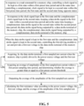
- a data strobe terminal and a complementary data strobe terminal of the semiconductor memory chip package may be configured to test electrical performance parameters of a semiconductor memory chip.
- a data strobe signal DQS acquired by the data strobe terminal and a complementary data strobe signal DQSn acquired by the complementary data strobe terminal are shown as pulse square wave signals in FIG. 1 , and as a result cannot be directly used for testing electrical performance parameters of a memory chip, and the data strobe terminal and the complementary data strobe terminal of the memory chip have test blind spots.
- a method for testing a memory chip including the following steps.
- step 22 in response to a read command for the memory chip, a clock signal is controlled to be kept in a first state within a first preset time period and at the same time a complementary clock signal is controlled to be kept in a second state within the first preset time period, the first state and the second state being opposite states.
- step 24 in response to the clock signal kept in the first state and the complementary clock signal kept in the second state, a data strobe signal is kept in the first state within a second preset time period and at the same time a complementary data strobe signal is kept in the second state within the second preset time period, the data strobe signal being outputted by a data strobe terminal of a memory chip, the complementary data strobe signal being outputted by a complementary data strobe terminal of the memory chip.
- step 26 when the data strobe signal is kept in the first state and the complementary data strobe signal is kept in the second state, a first driving module connected to the data strobe terminal is controlled to operate and measure a first resistance value and a second driving module connected to the complementary data strobe terminal is controlled to operate and measure a second resistance value.
- the clock signal of the memory chip is controlled to be kept in the first state such as a high level state within the first preset time period and at the same time the complementary clock signal of the memory chip is controlled to be kept in the second state such as a low level state within the first preset time period, the first state and the second state being opposite states.
- the clock signal is inputted into the memory chip through a clock terminal port of the memory chip, and the complementary clock signal is inputted into the memory chip through a complementary clock terminal port of the memory chip.
- the memory chip is controlled to respond to the read command for the memory chip, to enable the memory chip to keep, in response to the clock signal kept in the first state and the complementary clock signal kept in the second state, a data strobe signal in the first state within a second preset time period and at the same time keep a complementary data strobe signal in the second state within the second preset time period, the data strobe signal being outputted by a data strobe terminal of the memory chip, the complementary data strobe signal being outputted by a complementary data strobe terminal of the memory chip, so that while the data strobe signal is kept in the first state and the complementary data strobe signal is kept in the second state, the first driving module connected to the data strobe terminal is controlled to operate and measure the first resistance value and the second driving module connected to the complementary data strobe terminal is controlled to operate and measure the second resistance value.
- a read command for the memory chip is sent to a memory chip, the memory chip is controlled to keep a clock signal in a first state within a first preset time period and keep a complementary clock signal in a second state within the first preset time period, and a data strobe signal is kept in the first state within a second preset time period and at the same time a complementary data strobe signal is kept in the second state within the second preset time period, so that a test current or a test voltage can be acquired by a data strobe terminal and a complementary data strobe terminal, a first driving module connected to the data strobe terminal operates and measures a first resistance value, and a second driving module connected to the complementary data strobe terminal operates and measures a second resistance value, to determine, according to the measured first resistance value and second resistance value, whether there is an anomaly in the memory chip.
- the test method in this embodiment is simple and has low costs and an adequate test effect.
- the memory chip is controlled to respond to a read command for the memory chip Read CMD, and a clock signal CK of the memory chip is controlled to be kept in a high level state within the first preset time period and at the same time a complementary clock signal CKn of the memory chip is controlled to be kept in a low level state within the first preset time period.
- a clock signal CK of the memory chip is controlled to be kept in a high level state within the first preset time period and at the same time a complementary clock signal CKn of the memory chip is controlled to be kept in a low level state within the first preset time period.
- the first driving module connected to the data strobe terminal is controlled to operate and measure the first resistance value
- the second driving module connected to the complementary data strobe terminal is controlled to operate and measure the second resistance value
- the read command for the memory chip Read CMD is sent to the memory chip, the clock signal CK of the memory chip is controlled to be kept in a high level state within the first preset time period, and the complementary clock signal CKn is kept in a low level state within the first preset time period, to keep the data strobe signal in a high level state within the second preset time period and at the same time keep the complementary data strobe signal in a low level state within the second preset time period, so that a test current or a test voltage can be acquired by a data strobe terminal and a complementary data strobe terminal, the first driving module connected to the data strobe terminal operates and measures the first resistance value, and the second driving module connected to the complementary data strobe terminal operates and measures the second resistance value, to determine, according to the measured first resistance value and second resistance value, whether there is an anomaly in the memory chip.
- the test method in this embodiment is simple and has low costs and an adequate test effect.
- a time difference between a starting point t2 of the second preset time period and a starting point t1 of the first preset time period is an integer multiple of a value T of a clock period of the clock signal CK.
- a clock circuit such as a DLL circuit and/or a PLL circuit in the memory chip may enable a data strobe signal DQS to be kept in the first state and at the same time enable the complementary data strobe signal DQSn to be kept in the second state. That is, in the disclosure, inherent properties of a circuit inside the memory chip are used to implement the control of the data strobe signal DQS and the complementary data strobe signal DQSn, to enable a first driving circuit connected to the data strobe terminal to operate and measure the first resistance value and a second driving circuit connected to the complementary data strobe terminal to operate and measure the second resistance value.
- step 26 includes the following steps.
- step 261 when the data strobe signal is kept in the first state and the complementary data strobe signal is kept in the second state, the first driving module is controlled to act and provide a first test voltage to the data strobe terminal of the memory chip.
- step 262 the data strobe terminal acquires a first test current when the memory chip is jointly driven by a power source voltage and the first test voltage.
- the first resistance value is calculated according to the power source voltage, the first test voltage and the first test current.
- the first driving module may be controlled to act and provide a first test voltage to the data strobe terminal of the memory chip, and the data strobe terminal acquires the first test current when the memory chip is jointly driven by the power source voltage and the first test voltage.
- a method for testing a memory chip including the following steps.
- step 22 in response to a read command for the memory chip, a clock signal is controlled to be kept in a first state within a first preset time period and at the same time a complementary clock signal is controlled to be kept in a second state within the first preset time period, the first state and the second state being opposite states.
- step 24 in response to the clock signal kept in the first state and the complementary clock signal kept in the second state, a data strobe signal is kept in the first state within a second preset time period and at the same time a complementary data strobe signal is kept in the second state within the second preset time period, the data strobe signal being outputted by a data strobe terminal of a memory chip, the complementary data strobe signal being outputted by a complementary data strobe terminal of the memory chip.
- step 261 when the data strobe signal is kept in the first state and the complementary data strobe signal is kept in the second state, the first driving module is controlled to act and provide a first test voltage to the data strobe terminal of the memory chip.
- step 2621 a first sampled test current when the memory chip is jointly driven by the power source voltage and the first test voltage is acquired by the data strobe terminal.
- step 2622 an average of amplitudes of the first sampled test current within a first preset sampling time period is acquired, and it is determined whether the average is greater than or equal to a first preset current threshold.
- step 2623 if the average is greater than or equal to the first preset current threshold, the average of the amplitudes of the first sampled test current is outputted.
- the first resistance value is calculated according to the power source voltage, the first test voltage and the average of the amplitudes of the first sampled test current.
- the average of the amplitudes of the first sampled test current within the first preset sampling time period is acquired, and a first sampled test current with an average being greater than or equal to the first preset current threshold is acquired, to prevent excessive noise signals in the acquired first sampled test current, thereby avoiding affecting the accuracy of the first resistance value calculated according to the power source voltage, the first test voltage and the first test current.
- the calculating the first resistance value according to the power source voltage, the first test voltage and the average of the amplitudes of the first sampled test current includes:
- an output driving circuit when the memory chip is in a read data mode (an output driving mode) in response to the read command, an output driving circuit operates, a pull-up driving circuit operates, a pull-down driving circuit is turned off, and the pull-up driving circuit enables a data strobe terminal DQS to output a high level.
- the pull-up driving circuit is turned on, that is, the first driving module operates, and provides a first test voltage V Test1 to the data strobe terminal DQS, to measure equivalent resistance R pu of the pull-up driving circuit, that is, the first driving module according to Formula (1).
- step 24 differences between this embodiment of the disclosure and the embodiment shown in FIG. 5 lie in that, after step 24, the method further includes the following steps.
- step 264 when the data strobe signal is kept in the first state and the complementary data strobe signal is kept in the second state, the second driving module is controlled to act and provide a second test voltage to the complementary data strobe terminal of the memory chip.
- step 265 a second test current when the memory chip is driven by the second test voltage is acquired by the complementary data strobe terminal.
- step 266 the second resistance value is calculated according to the second test voltage and the second test current.
- the second driving module is controlled to act and provide the second test voltage to the complementary data strobe terminal of the memory chip, to calculate the second resistance value according to the second test voltage and the second test current.
- step 264 differences between this embodiment of the disclosure and the embodiment shown in FIG. 6 lie in that, after step 264, the method further includes the following steps.
- step 2651 a second sampled test current when the memory chip is driven by the second test voltage is acquired by the complementary data strobe terminal.
- step 2652 an average of amplitudes of the second sampled test current within a second preset sampling time period is acquired, and it is determined whether the average is greater than or equal to a second preset current threshold.
- step 2653 if the average is greater than or equal to the second preset current threshold, the average of the amplitudes of the second sampled test current is outputted.
- step 2661 the second resistance value is calculated according to the second test voltage and the average of the amplitudes of the second sampled test current.
- the obtained average of the amplitudes of the second sampled test current within the second preset sampling time period is acquired, and a second sampled test current with an average being greater than or equal to the second preset current threshold is acquired, to prevent excessive noise signals in the acquired second sampled test current, thereby avoiding affecting the accuracy of the second resistance value calculated according to the second test voltage and the second test current.
- the calculating the second resistance value according to the second test voltage and the average of the amplitudes of the second sampled test current includes:
- an output driving circuit when the memory chip is in a read data mode (an output driving mode) in response to the read command, an output driving circuit operates, a pull-down driving circuit operates, a pull-up driving circuit is turned off, and the pull-down driving circuit enables a complementary data strobe terminal DQSn to output a low level.
- the pull-down driving circuit is turned on, that is, the second driving module operates, and provides the second test voltage V Test2 to the complementary data strobe terminal DQSn, to measure the equivalent resistance R pd of the pull-down driving circuit, that is, a second driving circuit according to Formula (2).
- the method for testing a memory chip further includes the following step.
- step 267 when the clock signal is kept in the second state and the complementary clock signal is kept in the first state, a third driving module connected to the data strobe terminal is controlled to operate and measure a third resistance value, and a fourth driving module connected to the complementary data strobe terminal is controlled to operate and measure a fourth resistance value.
- the first driving module connected to the data strobe terminal is controlled to operate and measure the first resistance value
- the second driving module connected to the complementary data strobe terminal is controlled to operate and measure the second resistance value.
- the third driving module connected to the data strobe terminal is controlled to operate and measure the third resistance value
- the fourth driving module connected to the complementary data strobe terminal is controlled to operate and measure the fourth resistance value.
- comprehensive test of the memory chip can be implemented by the data strobe terminal and the complementary data strobe terminal.
- the first resistance value and the fourth resistance value acquired in two test processes may be compared, and the second resistance value and the third resistance value are compared, to assist in determining whether there is an anomaly in the memory chip.
- the first resistance value and the fourth resistance value are both equivalent resistance values obtained by measuring the pull-up driving circuit, and the second resistance value and the third resistance value are both equivalent resistance values obtained by measuring the pull-down driving circuit.
- a computer device may be a terminal, and an internal structural diagram of the terminal may be shown in FIG. 10 .
- the computer device includes a processor, a memory, a network interface, a display screen and an input device that are connected by a system bus.
- the processor of the computer device is configured to provide a computing and control capability.
- the memory of the computer device includes a non-volatile storage medium and internal memory.
- the non-volatile storage medium stores an operating system and a computer program.
- the computer program is executed by the processor to implement a method for testing a memory chip.
- the display screen of the computer device may be a liquid crystal display screen or an e-ink display screen.
- the input device of the computer device may be a touch layer covering the display screen, or may be a button, a trackball or a touchpad disposed on a housing of the computer device, or may be an external keyboard, a touchpad or mouse or the like.
- FIG. 10 is only a block diagram of a partial structure related to the solution of the disclosure, but does not constitute a limitation to the computer device on which the solution of the disclosure is applied.
- the specific computer device may include more or fewer components than those shown in the drawings, or some components may be combined, or different component arrangements are used.
- a computer-readable storage medium storing a computer program, the computer program being executed by a processor to implement the steps in the method for testing a memory chip in any embodiment of the disclosure.
- the computer program may be stored in a non-volatile computer-readable storage medium.
- the computer program is executed to perform the procedures in the foregoing embodiments of the methods.
- Any usage of a memory, storage, a database or another medium in the embodiments of the disclosure may include non-volatile and/or volatile memories.
- the non-volatile memory may include a read-only memory (ROM), a programmable ROM (PROM), an electrically programmable ROM (EPROM), an electrically erasable programmable ROM (EEPROM) or a flash memory.
- the volatile memory may include a random access memory (RAM) or an external cache memory.
- the RAM may be in various forms, for example, a static RAM (SRAM), a dynamic RAM (DRAM), a synchronous DRAM (SDRAM), a double data rate SDRAM (DDRSDRAM), an enhanced SDRAM (ESDRAM), a Synchlink DRAM (SLDRAM), a Rambus direct RAM (RDRAM), a Direct Rambus Dynamic RAM (DRDRAM), and a memory bus dynamic RAM (RDRAM).
- SRAM static RAM
- DRAM dynamic RAM
- SDRAM synchronous DRAM
- DDRSDRAM double data rate SDRAM
- ESDRAM enhanced SDRAM
- SLDRAM Synchlink DRAM
- RDRAM Rambus direct RAM
- DRAM Direct Rambus Dynamic RAM
- RDRAM memory bus dynamic RAM
Landscapes
- Tests Of Electronic Circuits (AREA)
Claims (13)
- Verfahren zum Testen eines Speicherchips, dadurch gekennzeichnet, dass das Verfahren Folgendes umfasst:als Reaktion auf einen Lesebefehl für den Speicherchip, Steuern eines Taktsignals des Speicherchips, sodass es in einem ersten Zustand innerhalb einer ersten voreingestellten Zeitspanne gehalten wird, und gleichzeitig Steuern eines komplementären Taktsignals des Speicherchips, sodass es in einem zweiten Zustand innerhalb der ersten voreingestellten Zeitspanne gehalten wird, wobei der erste Zustand und der zweite Zustand entgegengesetzte Zustände sind (22);als Reaktion auf das im ersten Zustand gehaltene Taktsignal und das im zweiten Zustand gehaltene komplementäre Taktsignal, Halten eines Datenimpulssignals im ersten Zustand innerhalb einer zweiten voreingestellten Zeitspanne und gleichzeitig Halten eines komplementären Datenimpulssignals im zweiten Zustand innerhalb der zweiten voreingestellten Zeitspanne, wobei das Datenimpulssignal von einem Datenimpulsendgerät des Speicherchips ausgegeben wird, wobei das komplementäre Datenimpulssignal von einem komplementären Datenimpulsendgerät des Speicherchips ausgegeben wird (24); undwenn das Datenimpulssignal in dem ersten Zustand gehalten wird und das komplementäre Datenimpulssignal in dem zweiten Zustand gehalten wird, Steuern einer ersten Pull-up-Treiberschaltung, die mit dem Datenimpulsendgerät verbunden ist, um betrieben zu werden, um einen ersten Widerstandswert der ersten Pull-up-Treiberschaltung messen zu können, und Steuern einer zweiten Pull-down-Treiberschaltung, die mit dem komplementären Datenimpulsendgerät verbunden ist, um betrieben zu werden, um einen zweiten Widerstandswert der zweiten Pull-down-Treiberschaltung messen zu können (26).
- Verfahren nach Anspruch 1, wobei das Steuern der ersten Pull-up-Treiberschaltung, die mit dem Datenimpulsendgerät verbunden ist, um betrieben zu werden, um den ersten Widerstandswert der ersten Pull-up-Treiberschaltung messen zu können, Folgendes umfasst:wenn das Taktsignal im ersten Zustand gehalten wird, Steuern der ersten Pull-up-Treiberschaltung, um zu agieren und eine erste Testspannung für das Datenimpulsendgerät des Speicherchips bereitzustellen (261);Erfassen, durch das Datenimpulsendgerät, eines ersten Teststroms, wenn der Speicherchip gemeinsam von einer Leistungsquellenspannung und der ersten Testspannung angetrieben wird (262); undBerechnen des ersten Widerstandswerts gemäß der Leistungsquellenspannung, der ersten Testspannung und dem ersten Teststrom (263).
- Verfahren nach Anspruch 2, wobei das Erfassen, durch das Datenimpulsendgerät, des ersten Teststroms, wenn der Speicherchip gemeinsam von der Leistungsquellenspannung und der ersten Testspannung angetrieben wird (262), Folgendes umfasst:Erfassen, durch das Datenimpulsendgerät, eines ersten abgetasteten Teststroms, wenn der Speicherchip gemeinsam von der Leistungsquellenspannung und der ersten Testspannung angetrieben wird (2621);Erfassen eines Mittelwerts von Amplituden des ersten abgetasteten Teststroms innerhalb einer ersten voreingestellten Abtastzeitspanne und Bestimmen, ob der Mittelwert größer oder gleich einem ersten voreingestellten Stromschwellenwert ist (2622);wenn der Mittelwert größer oder gleich dem ersten voreingestellten Stromschwellenwert ist, Ausgeben des Mittelwerts der Amplituden des ersten abgetasteten Teststroms (2623); undandernfalls erneutes Erfassen des ersten abgetasteten Teststroms.
- Verfahren nach Anspruch 3, wobei das Berechnen des ersten Widerstandswerts gemäß der Leistungsquellenspannung, der ersten Testspannung und dem ersten Teststrom (263) Folgendes umfasst:
Berechnen des ersten Widerstandswerts gemäß der Leistungsquellenspannung, der ersten Testspannung und dem Mittelwert der Amplituden des ersten abgetasteten Teststroms (2631). - Verfahren nach Anspruch 4, wobei das Berechnen des ersten Widerstandswerts gemäß der Leistungsquellenspannung, der ersten Testspannung und dem Mittelwert der Amplituden des ersten abgetasteten Teststroms (2631) Folgendes umfasst:Berechnen des ersten Widerstandswerts Rpu gemäß der folgenden Formel:
 wobei VDDQ die Leistungsquellenspannung ist, VTest1 die erste Testspannung ist und Iout1 der Mittelwert der Amplituden des ersten abgetasteten Teststroms ist.
 - Verfahren nach einem der Ansprüche 1 bis 5, wobei das Steuern der zweiten Pull-down-Treiberschaltung, die mit dem komplementären Datenimpulsendgerät verbunden ist, um betrieben zu werden, um den zweiten Widerstandswert der zweiten Pull-down-Treiberschaltung messen zu können, Folgendes umfasst:wenn das komplementäre Taktsignal im zweiten Zustand gehalten wird, Steuern der zweiten Pull-down-Treiberschaltung, um zu agieren und eine zweite Testspannung für das komplementäre Datenimpulsendgerät des Speicherchips bereitzustellen (264);Erfassen, durch das komplementäre Datenimpulsendgerät, eines zweiten Teststroms, wenn der Speicherchip durch die zweite Testspannung angetrieben wird (265); undBerechnen des zweiten Widerstandswerts gemäß der zweiten Testspannung und dem zweiten Teststrom (266).
- Verfahren nach Anspruch 6, wobei das Erfassen, durch das komplementäre Datenimpulsendgerät, eines zweiten Teststroms, wenn der Speicherchip durch die zweite Testspannung angetrieben wird (265), Folgendes umfasst:Erfassen, durch das komplementäre Datenimpulsendgerät, eines zweiten abgetasteten Teststroms, wenn der Speicherchip durch die zweite Testspannung angetrieben wird (2651);Erfassen eines Mittelwerts von Amplituden des zweiten abgetasteten Teststroms innerhalb einer zweiten voreingestellten Abtastzeitspanne und Bestimmen, ob der Mittelwert größer oder gleich einem zweiten voreingestellten Stromschwellenwert ist (2652);wenn der Mittelwert größer oder gleich dem zweiten voreingestellten Stromschwellenwert ist, Ausgeben des Mittelwerts der Amplituden des zweiten abgetasteten Teststroms (2653); undandernfalls erneutes Erfassen des zweiten abgetasteten Teststroms.
- Verfahren nach Anspruch 7, wobei das Berechnen des zweiten Widerstandswerts gemäß der zweiten Testspannung und dem zweiten Teststrom (266) Folgendes umfasst:
Berechnen des zweiten Widerstandswerts gemäß der zweiten Testspannung und dem Mittelwert der Amplituden des zweiten abgetasteten Teststroms (2661). - Verfahren nach Anspruch 8, wobei das Berechnen des zweiten Widerstandswerts gemäß der zweiten Testspannung und dem Mittelwert der Amplituden des zweiten abgetasteten Teststroms (2661) Folgendes umfasst:Berechnen des zweiten Widerstandswerts Rpd gemäß der folgenden Formel:
 wobei VTest2 die zweite Testspannung ist und Iout2 der Mittelwert der Amplituden des zweiten abgetasteten Teststroms ist.
 - Verfahren nach einem der Ansprüche 1 bis 5, wobei eine Zeitdifferenz zwischen einem Startpunkt der zweiten voreingestellten Zeitspanne und einem Startpunkt der ersten voreingestellten Zeitspanne ein ganzzahliges Vielfaches eines Wertes einer Taktperiode des Taktsignals ist.
- Verfahren nach einem der Ansprüche 1 bis 5, ferner umfassend:
wenn das Taktsignal in dem zweiten Zustand gehalten wird und das komplementäre Taktsignal in dem ersten Zustand gehalten wird, Steuern einer dritten Pull-up-Treiberschaltung, die mit dem Datenimpulsendgerät verbunden ist, um betrieben zu werden, um einen dritten Widerstandswert der dritten Pull-up-Treiberschaltung messen zu können, und Steuern einer vierten Pull-down-Treiberschaltung, die mit dem komplementären Datenimpulsendgerät verbunden ist, um betrieben zu werden, um einen vierten Widerstandswert der vierten Pull-down-Treiberschaltung messen zu können (267). - Rechnervorrichtung, die Mittel zum Umsetzen der Schritte des Verfahrens nach einem der Ansprüche 1 bis 11 umfasst.
- Computerlesbares Speichermedium, das ein Computerprogramm speichert, wobei das Computerprogramm von einem Prozessor ausgeführt wird, um die Schritte des Verfahrens nach einem der Ansprüche 1 bis 11 umzusetzen.
Applications Claiming Priority (2)
| Application Number | Priority Date | Filing Date | Title |
|---|---|---|---|
| CN202110441989.XA CN115240748B (zh) | 2021-04-23 | 2021-04-23 | 存储芯片测试方法、计算机设备及介质 |
| PCT/CN2021/112894 WO2022222327A1 (zh) | 2021-04-23 | 2021-08-17 | 存储芯片测试方法、计算机设备及介质 |
Publications (3)
| Publication Number | Publication Date |
|---|---|
| EP4099330A1 EP4099330A1 (de) | 2022-12-07 |
| EP4099330A4 EP4099330A4 (de) | 2023-06-07 |
| EP4099330B1 true EP4099330B1 (de) | 2025-04-09 |
Family
ID=83693389
Family Applications (1)
| Application Number | Title | Priority Date | Filing Date |
|---|---|---|---|
| EP21876735.8A Active EP4099330B1 (de) | 2021-04-23 | 2021-08-17 | Speicherchiptestverfahren, computervorrichtung und medium |
Country Status (2)
| Country | Link |
|---|---|
| US (1) | US11721411B2 (de) |
| EP (1) | EP4099330B1 (de) |
Families Citing this family (2)
| Publication number | Priority date | Publication date | Assignee | Title |
|---|---|---|---|---|
| FR3130132B1 (fr) | 2021-12-09 | 2023-11-17 | Oreal | Dispersion comprenant une particule polymerique, un agent stabilisant a groupe cycloalkyle, une huile, et de l’eau, procede de traitement des matieres keratiniques mettant en œuvre la dispersion |
| CN115840130A (zh) * | 2022-12-06 | 2023-03-24 | 安测半导体技术(义乌)有限公司 | 射频芯片的自动补偿方法及系统、设备及介质 |
Family Cites Families (9)
| Publication number | Priority date | Publication date | Assignee | Title |
|---|---|---|---|---|
| JP4075140B2 (ja) | 1998-06-25 | 2008-04-16 | 富士通株式会社 | 電子装置及び半導体記憶装置 |
| JP2000074986A (ja) * | 1998-08-31 | 2000-03-14 | Ando Electric Co Ltd | デバイス試験装置 |
| KR100557636B1 (ko) | 2003-12-23 | 2006-03-10 | 주식회사 하이닉스반도체 | 클럭신호를 이용한 데이터 스트로브 회로 |
| KR100605590B1 (ko) * | 2004-05-10 | 2006-07-31 | 주식회사 하이닉스반도체 | 데이터 출력드라이버의 임피던스를 조정할 수 있는 반도체메모리 장치 |
| JP2007036546A (ja) * | 2005-07-26 | 2007-02-08 | Nec Electronics Corp | インピーダンス調整回路と方法 |
| KR100640158B1 (ko) * | 2005-09-27 | 2006-11-01 | 주식회사 하이닉스반도체 | 데이터 출력드라이버의 임피던스를 조정할 수 있는 반도체메모리 장치 |
| KR100733430B1 (ko) | 2005-09-29 | 2007-06-29 | 주식회사 하이닉스반도체 | 반도체 메모리 장치 |
| CN106875966B (zh) | 2017-01-09 | 2020-02-07 | 上海兆芯集成电路有限公司 | 数据选通信号处理系统以及处理方法 |
| US10803914B1 (en) | 2019-08-27 | 2020-10-13 | Micron Technology, Inc. | Selectively squelching differential strobe input signal in memory-device testing system |
-
2021
- 2021-08-17 EP EP21876735.8A patent/EP4099330B1/de active Active
-
2022
- 2022-02-11 US US17/669,520 patent/US11721411B2/en active Active
Also Published As
| Publication number | Publication date |
|---|---|
| EP4099330A4 (de) | 2023-06-07 |
| EP4099330A1 (de) | 2022-12-07 |
| US20220343997A1 (en) | 2022-10-27 |
| US11721411B2 (en) | 2023-08-08 |
Similar Documents
| Publication | Publication Date | Title |
|---|---|---|
| EP4099330B1 (de) | Speicherchiptestverfahren, computervorrichtung und medium | |
| EP2430634B1 (de) | Verfahren zur kalibrierung von startwerten zur schreibvorgangsnivellierung in einem speichersystem | |
| US6456544B1 (en) | Selective forwarding of a strobe based on a predetermined delay following a memory read command | |
| EP0855653B1 (de) | Speichersteuerungsvorrichtung mit programmierbarer Impulsverzögerung | |
| JP2007116574A (ja) | Dll回路及びこれらを備えた半導体装置 | |
| EP2015309A1 (de) | Oszillator, Verfahren zu seiner Einstellung und Speicher | |
| US6871306B2 (en) | Method and device for reading and for checking the time position of data response signals read out from a memory module to be tested | |
| US6876219B2 (en) | Test configuration with automatic test machine and integrated circuit and method for determining the time behavior of an integrated circuit | |
| JPH027530B2 (de) | ||
| US6215345B1 (en) | Semiconductor device for setting delay time | |
| DE112004003057A1 (de) | Adaptive Eingabe/Ausgabe-Puffer und Verfahren dafür | |
| CN115240748B (zh) | 存储芯片测试方法、计算机设备及介质 | |
| US6418547B1 (en) | Internal guardband for semiconductor testing | |
| US6327218B1 (en) | Integrated circuit time delay measurement apparatus | |
| US20170163250A1 (en) | Delay circuit and test method of delay circuit | |
| RU2363059C2 (ru) | Адаптивная калибровка памяти с использованием бункеров | |
| CN100517515C (zh) | 测定方法及测定系统 | |
| US11817165B2 (en) | Signal generation circuit and method, and semiconductor memory | |
| KR102718902B1 (ko) | 메모리 | |
| US20070247958A1 (en) | Column selection signal generator for semiconductor memory | |
| CN115902585A (zh) | 一种设备Wi-Fi的调测方法、装置、系统及设备 | |
| CN111010181B (zh) | 一种ddr信号时序校准方法和装置 | |
| KR20240007735A (ko) | 메모리, 제어 장치, 클럭 처리 방법과 전자 기기 | |
| US8120983B2 (en) | Semiconductor device having plurality of operation modes | |
| KR102897879B1 (ko) | 제어 장치, 메모리, 신호 처리 방법 및 전자 기기 |
Legal Events
| Date | Code | Title | Description |
|---|---|---|---|
| STAA | Information on the status of an ep patent application or granted ep patent |
Free format text: STATUS: UNKNOWN |
|
| STAA | Information on the status of an ep patent application or granted ep patent |
Free format text: STATUS: THE INTERNATIONAL PUBLICATION HAS BEEN MADE |
|
| PUAI | Public reference made under article 153(3) epc to a published international application that has entered the european phase |
Free format text: ORIGINAL CODE: 0009012 |
|
| STAA | Information on the status of an ep patent application or granted ep patent |
Free format text: STATUS: REQUEST FOR EXAMINATION WAS MADE |
|
| 17P | Request for examination filed |
Effective date: 20220422 |
|
| AK | Designated contracting states |
Kind code of ref document: A1 Designated state(s): AL AT BE BG CH CY CZ DE DK EE ES FI FR GB GR HR HU IE IS IT LI LT LU LV MC MK MT NL NO PL PT RO RS SE SI SK SM TR |
|
| A4 | Supplementary search report drawn up and despatched |
Effective date: 20230509 |
|
| RIC1 | Information provided on ipc code assigned before grant |
Ipc: G11C 29/02 20060101ALI20230502BHEP Ipc: G11C 29/50 20060101ALI20230502BHEP Ipc: G11C 29/12 20060101AFI20230502BHEP |
|
| DAV | Request for validation of the european patent (deleted) | ||
| DAX | Request for extension of the european patent (deleted) | ||
| GRAP | Despatch of communication of intention to grant a patent |
Free format text: ORIGINAL CODE: EPIDOSNIGR1 |
|
| STAA | Information on the status of an ep patent application or granted ep patent |
Free format text: STATUS: GRANT OF PATENT IS INTENDED |
|
| INTG | Intention to grant announced |
Effective date: 20241128 |
|
| P01 | Opt-out of the competence of the unified patent court (upc) registered |
Free format text: CASE NUMBER: APP_1891/2025 Effective date: 20250111 |
|
| GRAS | Grant fee paid |
Free format text: ORIGINAL CODE: EPIDOSNIGR3 |
|
| GRAA | (expected) grant |
Free format text: ORIGINAL CODE: 0009210 |
|
| STAA | Information on the status of an ep patent application or granted ep patent |
Free format text: STATUS: THE PATENT HAS BEEN GRANTED |
|
| AK | Designated contracting states |
Kind code of ref document: B1 Designated state(s): AL AT BE BG CH CY CZ DE DK EE ES FI FR GB GR HR HU IE IS IT LI LT LU LV MC MK MT NL NO PL PT RO RS SE SI SK SM TR |
|
| REG | Reference to a national code |
Ref country code: GB Ref legal event code: FG4D |
|
| REG | Reference to a national code |
Ref country code: CH Ref legal event code: EP |
|
| REG | Reference to a national code |
Ref country code: DE Ref legal event code: R096 Ref document number: 602021029061 Country of ref document: DE |
|
| REG | Reference to a national code |
Ref country code: IE Ref legal event code: FG4D |
|
| REG | Reference to a national code |
Ref country code: NL Ref legal event code: MP Effective date: 20250409 |
|
| PG25 | Lapsed in a contracting state [announced via postgrant information from national office to epo] |
Ref country code: NL Free format text: LAPSE BECAUSE OF FAILURE TO SUBMIT A TRANSLATION OF THE DESCRIPTION OR TO PAY THE FEE WITHIN THE PRESCRIBED TIME-LIMIT Effective date: 20250409 |
|
| REG | Reference to a national code |
Ref country code: AT Ref legal event code: MK05 Ref document number: 1784309 Country of ref document: AT Kind code of ref document: T Effective date: 20250409 |
|
| PG25 | Lapsed in a contracting state [announced via postgrant information from national office to epo] |
Ref country code: FI Free format text: LAPSE BECAUSE OF FAILURE TO SUBMIT A TRANSLATION OF THE DESCRIPTION OR TO PAY THE FEE WITHIN THE PRESCRIBED TIME-LIMIT Effective date: 20250409 Ref country code: PT Free format text: LAPSE BECAUSE OF FAILURE TO SUBMIT A TRANSLATION OF THE DESCRIPTION OR TO PAY THE FEE WITHIN THE PRESCRIBED TIME-LIMIT Effective date: 20250811 Ref country code: ES Free format text: LAPSE BECAUSE OF FAILURE TO SUBMIT A TRANSLATION OF THE DESCRIPTION OR TO PAY THE FEE WITHIN THE PRESCRIBED TIME-LIMIT Effective date: 20250409 |
|
| PGFP | Annual fee paid to national office [announced via postgrant information from national office to epo] |
Ref country code: DE Payment date: 20250820 Year of fee payment: 5 |
|
| REG | Reference to a national code |
Ref country code: LT Ref legal event code: MG9D |
|
| PG25 | Lapsed in a contracting state [announced via postgrant information from national office to epo] |
Ref country code: NO Free format text: LAPSE BECAUSE OF FAILURE TO SUBMIT A TRANSLATION OF THE DESCRIPTION OR TO PAY THE FEE WITHIN THE PRESCRIBED TIME-LIMIT Effective date: 20250709 Ref country code: GR Free format text: LAPSE BECAUSE OF FAILURE TO SUBMIT A TRANSLATION OF THE DESCRIPTION OR TO PAY THE FEE WITHIN THE PRESCRIBED TIME-LIMIT Effective date: 20250710 |
|
| PG25 | Lapsed in a contracting state [announced via postgrant information from national office to epo] |
Ref country code: PL Free format text: LAPSE BECAUSE OF FAILURE TO SUBMIT A TRANSLATION OF THE DESCRIPTION OR TO PAY THE FEE WITHIN THE PRESCRIBED TIME-LIMIT Effective date: 20250409 |
|
| PG25 | Lapsed in a contracting state [announced via postgrant information from national office to epo] |
Ref country code: BG Free format text: LAPSE BECAUSE OF FAILURE TO SUBMIT A TRANSLATION OF THE DESCRIPTION OR TO PAY THE FEE WITHIN THE PRESCRIBED TIME-LIMIT Effective date: 20250409 |
|
| PG25 | Lapsed in a contracting state [announced via postgrant information from national office to epo] |
Ref country code: HR Free format text: LAPSE BECAUSE OF FAILURE TO SUBMIT A TRANSLATION OF THE DESCRIPTION OR TO PAY THE FEE WITHIN THE PRESCRIBED TIME-LIMIT Effective date: 20250409 |
|
| PG25 | Lapsed in a contracting state [announced via postgrant information from national office to epo] |
Ref country code: AT Free format text: LAPSE BECAUSE OF FAILURE TO SUBMIT A TRANSLATION OF THE DESCRIPTION OR TO PAY THE FEE WITHIN THE PRESCRIBED TIME-LIMIT Effective date: 20250409 |
|
| PG25 | Lapsed in a contracting state [announced via postgrant information from national office to epo] |
Ref country code: RS Free format text: LAPSE BECAUSE OF FAILURE TO SUBMIT A TRANSLATION OF THE DESCRIPTION OR TO PAY THE FEE WITHIN THE PRESCRIBED TIME-LIMIT Effective date: 20250709 |
|
| PG25 | Lapsed in a contracting state [announced via postgrant information from national office to epo] |
Ref country code: IS Free format text: LAPSE BECAUSE OF FAILURE TO SUBMIT A TRANSLATION OF THE DESCRIPTION OR TO PAY THE FEE WITHIN THE PRESCRIBED TIME-LIMIT Effective date: 20250809 |
|
| PG25 | Lapsed in a contracting state [announced via postgrant information from national office to epo] |
Ref country code: LV Free format text: LAPSE BECAUSE OF FAILURE TO SUBMIT A TRANSLATION OF THE DESCRIPTION OR TO PAY THE FEE WITHIN THE PRESCRIBED TIME-LIMIT Effective date: 20250409 |
|
| REG | Reference to a national code |
Ref country code: DE Ref legal event code: R097 Ref document number: 602021029061 Country of ref document: DE |
|
| PG25 | Lapsed in a contracting state [announced via postgrant information from national office to epo] |
Ref country code: DK Free format text: LAPSE BECAUSE OF FAILURE TO SUBMIT A TRANSLATION OF THE DESCRIPTION OR TO PAY THE FEE WITHIN THE PRESCRIBED TIME-LIMIT Effective date: 20250409 Ref country code: SM Free format text: LAPSE BECAUSE OF FAILURE TO SUBMIT A TRANSLATION OF THE DESCRIPTION OR TO PAY THE FEE WITHIN THE PRESCRIBED TIME-LIMIT Effective date: 20250409 |
|
| PG25 | Lapsed in a contracting state [announced via postgrant information from national office to epo] |
Ref country code: CZ Free format text: LAPSE BECAUSE OF FAILURE TO SUBMIT A TRANSLATION OF THE DESCRIPTION OR TO PAY THE FEE WITHIN THE PRESCRIBED TIME-LIMIT Effective date: 20250409 |
|
| PG25 | Lapsed in a contracting state [announced via postgrant information from national office to epo] |
Ref country code: EE Free format text: LAPSE BECAUSE OF FAILURE TO SUBMIT A TRANSLATION OF THE DESCRIPTION OR TO PAY THE FEE WITHIN THE PRESCRIBED TIME-LIMIT Effective date: 20250409 |
|
| PG25 | Lapsed in a contracting state [announced via postgrant information from national office to epo] |
Ref country code: SK Free format text: LAPSE BECAUSE OF FAILURE TO SUBMIT A TRANSLATION OF THE DESCRIPTION OR TO PAY THE FEE WITHIN THE PRESCRIBED TIME-LIMIT Effective date: 20250409 |
|
| PG25 | Lapsed in a contracting state [announced via postgrant information from national office to epo] |
Ref country code: IT Free format text: LAPSE BECAUSE OF FAILURE TO SUBMIT A TRANSLATION OF THE DESCRIPTION OR TO PAY THE FEE WITHIN THE PRESCRIBED TIME-LIMIT Effective date: 20250409 |
|
| PG25 | Lapsed in a contracting state [announced via postgrant information from national office to epo] |
Ref country code: RO Free format text: LAPSE BECAUSE OF FAILURE TO SUBMIT A TRANSLATION OF THE DESCRIPTION OR TO PAY THE FEE WITHIN THE PRESCRIBED TIME-LIMIT Effective date: 20250409 |
|
| PLBE | No opposition filed within time limit |
Free format text: ORIGINAL CODE: 0009261 |
|
| STAA | Information on the status of an ep patent application or granted ep patent |
Free format text: STATUS: NO OPPOSITION FILED WITHIN TIME LIMIT |
|
| REG | Reference to a national code |
Ref country code: CH Ref legal event code: L10 Free format text: ST27 STATUS EVENT CODE: U-0-0-L10-L00 (AS PROVIDED BY THE NATIONAL OFFICE) Effective date: 20260218 |
|
| 26N | No opposition filed |
Effective date: 20260112 |
|
| REG | Reference to a national code |
Ref country code: CH Ref legal event code: H13 Free format text: ST27 STATUS EVENT CODE: U-0-0-H10-H13 (AS PROVIDED BY THE NATIONAL OFFICE) Effective date: 20260324 |
|
| PG25 | Lapsed in a contracting state [announced via postgrant information from national office to epo] |
Ref country code: MC Free format text: LAPSE BECAUSE OF FAILURE TO SUBMIT A TRANSLATION OF THE DESCRIPTION OR TO PAY THE FEE WITHIN THE PRESCRIBED TIME-LIMIT Effective date: 20250409 |
|
| PG25 | Lapsed in a contracting state [announced via postgrant information from national office to epo] |
Ref country code: LU Free format text: LAPSE BECAUSE OF NON-PAYMENT OF DUE FEES Effective date: 20250817 |