EP4092897B1 - Bidirektionaler gleichstromwandler und steuerungsverfahren dafür sowie vorrichtung dafür und speichermedium - Google Patents
Bidirektionaler gleichstromwandler und steuerungsverfahren dafür sowie vorrichtung dafür und speichermedium Download PDFInfo
- Publication number
- EP4092897B1 EP4092897B1 EP21921637.1A EP21921637A EP4092897B1 EP 4092897 B1 EP4092897 B1 EP 4092897B1 EP 21921637 A EP21921637 A EP 21921637A EP 4092897 B1 EP4092897 B1 EP 4092897B1
- Authority
- EP
- European Patent Office
- Prior art keywords
- voltage
- voltage value
- switching tube
- bridge arm
- control cycle
- Prior art date
- Legal status (The legal status is an assumption and is not a legal conclusion. Google has not performed a legal analysis and makes no representation as to the accuracy of the status listed.)
- Active
Links
Images

Classifications
-
- H—ELECTRICITY
- H02—GENERATION; CONVERSION OR DISTRIBUTION OF ELECTRIC POWER
- H02M—APPARATUS FOR CONVERSION BETWEEN AC AND AC, BETWEEN AC AND DC, OR BETWEEN DC AND DC, AND FOR USE WITH MAINS OR SIMILAR POWER SUPPLY SYSTEMS; CONVERSION OF DC OR AC INPUT POWER INTO SURGE OUTPUT POWER; CONTROL OR REGULATION THEREOF
- H02M1/00—Details of apparatus for conversion
- H02M1/0003—Details of control, feedback or regulation circuits
- H02M1/0025—Arrangements for modifying reference values, feedback values or error values in the control loop of a converter
-
- H—ELECTRICITY
- H02—GENERATION; CONVERSION OR DISTRIBUTION OF ELECTRIC POWER
- H02M—APPARATUS FOR CONVERSION BETWEEN AC AND AC, BETWEEN AC AND DC, OR BETWEEN DC AND DC, AND FOR USE WITH MAINS OR SIMILAR POWER SUPPLY SYSTEMS; CONVERSION OF DC OR AC INPUT POWER INTO SURGE OUTPUT POWER; CONTROL OR REGULATION THEREOF
- H02M3/00—Conversion of DC power input into DC power output
- H02M3/22—Conversion of DC power input into DC power output with intermediate conversion into AC
- H02M3/24—Conversion of DC power input into DC power output with intermediate conversion into AC by static converters
- H02M3/28—Conversion of DC power input into DC power output with intermediate conversion into AC by static converters using discharge tubes with control electrode or semiconductor devices with control electrode to produce the intermediate AC
- H02M3/325—Conversion of DC power input into DC power output with intermediate conversion into AC by static converters using discharge tubes with control electrode or semiconductor devices with control electrode to produce the intermediate AC using devices of a triode or a transistor type requiring continuous application of a control signal
- H02M3/335—Conversion of DC power input into DC power output with intermediate conversion into AC by static converters using discharge tubes with control electrode or semiconductor devices with control electrode to produce the intermediate AC using devices of a triode or a transistor type requiring continuous application of a control signal using semiconductor devices only
- H02M3/33569—Conversion of DC power input into DC power output with intermediate conversion into AC by static converters using discharge tubes with control electrode or semiconductor devices with control electrode to produce the intermediate AC using devices of a triode or a transistor type requiring continuous application of a control signal using semiconductor devices only having several active switching elements
- H02M3/33576—Conversion of DC power input into DC power output with intermediate conversion into AC by static converters using discharge tubes with control electrode or semiconductor devices with control electrode to produce the intermediate AC using devices of a triode or a transistor type requiring continuous application of a control signal using semiconductor devices only having several active switching elements having at least one active switching element at the secondary side of an isolation transformer
- H02M3/33584—Bidirectional converters
-
- H—ELECTRICITY
- H02—GENERATION; CONVERSION OR DISTRIBUTION OF ELECTRIC POWER
- H02M—APPARATUS FOR CONVERSION BETWEEN AC AND AC, BETWEEN AC AND DC, OR BETWEEN DC AND DC, AND FOR USE WITH MAINS OR SIMILAR POWER SUPPLY SYSTEMS; CONVERSION OF DC OR AC INPUT POWER INTO SURGE OUTPUT POWER; CONTROL OR REGULATION THEREOF
- H02M3/00—Conversion of DC power input into DC power output
- H02M3/22—Conversion of DC power input into DC power output with intermediate conversion into AC
- H02M3/24—Conversion of DC power input into DC power output with intermediate conversion into AC by static converters
- H02M3/28—Conversion of DC power input into DC power output with intermediate conversion into AC by static converters using discharge tubes with control electrode or semiconductor devices with control electrode to produce the intermediate AC
- H02M3/325—Conversion of DC power input into DC power output with intermediate conversion into AC by static converters using discharge tubes with control electrode or semiconductor devices with control electrode to produce the intermediate AC using devices of a triode or a transistor type requiring continuous application of a control signal
- H02M3/335—Conversion of DC power input into DC power output with intermediate conversion into AC by static converters using discharge tubes with control electrode or semiconductor devices with control electrode to produce the intermediate AC using devices of a triode or a transistor type requiring continuous application of a control signal using semiconductor devices only
- H02M3/3353—Conversion of DC power input into DC power output with intermediate conversion into AC by static converters using discharge tubes with control electrode or semiconductor devices with control electrode to produce the intermediate AC using devices of a triode or a transistor type requiring continuous application of a control signal using semiconductor devices only having at least two simultaneously operating switches on the input side, e.g. "double forward" or "double (switched) flyback" converter
-
- B—PERFORMING OPERATIONS; TRANSPORTING
- B60—VEHICLES IN GENERAL
- B60L—PROPULSION OF ELECTRICALLY-PROPELLED VEHICLES; SUPPLYING ELECTRIC POWER FOR AUXILIARY EQUIPMENT OF ELECTRICALLY-PROPELLED VEHICLES; ELECTRODYNAMIC BRAKE SYSTEMS FOR VEHICLES IN GENERAL; MAGNETIC SUSPENSION OR LEVITATION FOR VEHICLES; MONITORING OPERATING VARIABLES OF ELECTRICALLY-PROPELLED VEHICLES; ELECTRIC SAFETY DEVICES FOR ELECTRICALLY-PROPELLED VEHICLES
- B60L53/00—Methods of charging batteries, specially adapted for electric vehicles; Charging stations or on-board charging equipment therefor; Exchange of energy storage elements in electric vehicles
- B60L53/10—Methods of charging batteries, specially adapted for electric vehicles; Charging stations or on-board charging equipment therefor; Exchange of energy storage elements in electric vehicles characterised by the energy transfer between the charging station and the vehicle
- B60L53/11—DC charging controlled by the charging station, e.g. mode 4
-
- B—PERFORMING OPERATIONS; TRANSPORTING
- B60—VEHICLES IN GENERAL
- B60L—PROPULSION OF ELECTRICALLY-PROPELLED VEHICLES; SUPPLYING ELECTRIC POWER FOR AUXILIARY EQUIPMENT OF ELECTRICALLY-PROPELLED VEHICLES; ELECTRODYNAMIC BRAKE SYSTEMS FOR VEHICLES IN GENERAL; MAGNETIC SUSPENSION OR LEVITATION FOR VEHICLES; MONITORING OPERATING VARIABLES OF ELECTRICALLY-PROPELLED VEHICLES; ELECTRIC SAFETY DEVICES FOR ELECTRICALLY-PROPELLED VEHICLES
- B60L53/00—Methods of charging batteries, specially adapted for electric vehicles; Charging stations or on-board charging equipment therefor; Exchange of energy storage elements in electric vehicles
- B60L53/20—Methods of charging batteries, specially adapted for electric vehicles; Charging stations or on-board charging equipment therefor; Exchange of energy storage elements in electric vehicles characterised by converters located in the vehicle
- B60L53/24—Using the vehicle's propulsion converter for charging
-
- H—ELECTRICITY
- H02—GENERATION; CONVERSION OR DISTRIBUTION OF ELECTRIC POWER
- H02J—ELECTRIC POWER NETWORKS; CIRCUIT ARRANGEMENTS OR SYSTEMS FOR SUPPLYING OR DISTRIBUTING ELECTRIC POWER; SYSTEMS FOR STORING ELECTRIC ENERGY
- H02J7/00—Circuit arrangements for charging or discharging batteries or for supplying loads from batteries
- H02J7/02—Circuit arrangements for charging or discharging batteries or for supplying loads from batteries for charging batteries from AC mains by converters
-
- H—ELECTRICITY
- H02—GENERATION; CONVERSION OR DISTRIBUTION OF ELECTRIC POWER
- H02J—ELECTRIC POWER NETWORKS; CIRCUIT ARRANGEMENTS OR SYSTEMS FOR SUPPLYING OR DISTRIBUTING ELECTRIC POWER; SYSTEMS FOR STORING ELECTRIC ENERGY
- H02J7/00—Circuit arrangements for charging or discharging batteries or for supplying loads from batteries
- H02J7/90—Regulation of charging or discharging current or voltage
-
- H—ELECTRICITY
- H02—GENERATION; CONVERSION OR DISTRIBUTION OF ELECTRIC POWER
- H02J—ELECTRIC POWER NETWORKS; CIRCUIT ARRANGEMENTS OR SYSTEMS FOR SUPPLYING OR DISTRIBUTING ELECTRIC POWER; SYSTEMS FOR STORING ELECTRIC ENERGY
- H02J7/00—Circuit arrangements for charging or discharging batteries or for supplying loads from batteries
- H02J7/90—Regulation of charging or discharging current or voltage
- H02J7/92—Regulation of charging or discharging current or voltage with prioritisation of loads or sources
-
- H—ELECTRICITY
- H02—GENERATION; CONVERSION OR DISTRIBUTION OF ELECTRIC POWER
- H02M—APPARATUS FOR CONVERSION BETWEEN AC AND AC, BETWEEN AC AND DC, OR BETWEEN DC AND DC, AND FOR USE WITH MAINS OR SIMILAR POWER SUPPLY SYSTEMS; CONVERSION OF DC OR AC INPUT POWER INTO SURGE OUTPUT POWER; CONTROL OR REGULATION THEREOF
- H02M1/00—Details of apparatus for conversion
- H02M1/0003—Details of control, feedback or regulation circuits
- H02M1/0012—Control circuits using digital or numerical techniques
-
- H—ELECTRICITY
- H02—GENERATION; CONVERSION OR DISTRIBUTION OF ELECTRIC POWER
- H02M—APPARATUS FOR CONVERSION BETWEEN AC AND AC, BETWEEN AC AND DC, OR BETWEEN DC AND DC, AND FOR USE WITH MAINS OR SIMILAR POWER SUPPLY SYSTEMS; CONVERSION OF DC OR AC INPUT POWER INTO SURGE OUTPUT POWER; CONTROL OR REGULATION THEREOF
- H02M1/00—Details of apparatus for conversion
- H02M1/08—Circuits specially adapted for the generation of control voltages for semiconductor devices incorporated in static converters
- H02M1/088—Circuits specially adapted for the generation of control voltages for semiconductor devices incorporated in static converters for the simultaneous control of series or parallel connected semiconductor devices
-
- H—ELECTRICITY
- H02—GENERATION; CONVERSION OR DISTRIBUTION OF ELECTRIC POWER
- H02M—APPARATUS FOR CONVERSION BETWEEN AC AND AC, BETWEEN AC AND DC, OR BETWEEN DC AND DC, AND FOR USE WITH MAINS OR SIMILAR POWER SUPPLY SYSTEMS; CONVERSION OF DC OR AC INPUT POWER INTO SURGE OUTPUT POWER; CONTROL OR REGULATION THEREOF
- H02M3/00—Conversion of DC power input into DC power output
- H02M3/01—Resonant DC/DC converters
-
- H—ELECTRICITY
- H02—GENERATION; CONVERSION OR DISTRIBUTION OF ELECTRIC POWER
- H02M—APPARATUS FOR CONVERSION BETWEEN AC AND AC, BETWEEN AC AND DC, OR BETWEEN DC AND DC, AND FOR USE WITH MAINS OR SIMILAR POWER SUPPLY SYSTEMS; CONVERSION OF DC OR AC INPUT POWER INTO SURGE OUTPUT POWER; CONTROL OR REGULATION THEREOF
- H02M3/00—Conversion of DC power input into DC power output
- H02M3/02—Conversion of DC power input into DC power output without intermediate conversion into AC
- H02M3/04—Conversion of DC power input into DC power output without intermediate conversion into AC by static converters
- H02M3/10—Conversion of DC power input into DC power output without intermediate conversion into AC by static converters using discharge tubes with control electrode or semiconductor devices with control electrode
- H02M3/145—Conversion of DC power input into DC power output without intermediate conversion into AC by static converters using discharge tubes with control electrode or semiconductor devices with control electrode using devices of a triode or transistor type requiring continuous application of a control signal
- H02M3/155—Conversion of DC power input into DC power output without intermediate conversion into AC by static converters using discharge tubes with control electrode or semiconductor devices with control electrode using devices of a triode or transistor type requiring continuous application of a control signal using semiconductor devices only
- H02M3/156—Conversion of DC power input into DC power output without intermediate conversion into AC by static converters using discharge tubes with control electrode or semiconductor devices with control electrode using devices of a triode or transistor type requiring continuous application of a control signal using semiconductor devices only with automatic control of output voltage or current, e.g. switching regulators
- H02M3/157—Conversion of DC power input into DC power output without intermediate conversion into AC by static converters using discharge tubes with control electrode or semiconductor devices with control electrode using devices of a triode or transistor type requiring continuous application of a control signal using semiconductor devices only with automatic control of output voltage or current, e.g. switching regulators with digital control
-
- H—ELECTRICITY
- H02—GENERATION; CONVERSION OR DISTRIBUTION OF ELECTRIC POWER
- H02M—APPARATUS FOR CONVERSION BETWEEN AC AND AC, BETWEEN AC AND DC, OR BETWEEN DC AND DC, AND FOR USE WITH MAINS OR SIMILAR POWER SUPPLY SYSTEMS; CONVERSION OF DC OR AC INPUT POWER INTO SURGE OUTPUT POWER; CONTROL OR REGULATION THEREOF
- H02M3/00—Conversion of DC power input into DC power output
- H02M3/22—Conversion of DC power input into DC power output with intermediate conversion into AC
- H02M3/24—Conversion of DC power input into DC power output with intermediate conversion into AC by static converters
- H02M3/28—Conversion of DC power input into DC power output with intermediate conversion into AC by static converters using discharge tubes with control electrode or semiconductor devices with control electrode to produce the intermediate AC
-
- H—ELECTRICITY
- H02—GENERATION; CONVERSION OR DISTRIBUTION OF ELECTRIC POWER
- H02M—APPARATUS FOR CONVERSION BETWEEN AC AND AC, BETWEEN AC AND DC, OR BETWEEN DC AND DC, AND FOR USE WITH MAINS OR SIMILAR POWER SUPPLY SYSTEMS; CONVERSION OF DC OR AC INPUT POWER INTO SURGE OUTPUT POWER; CONTROL OR REGULATION THEREOF
- H02M3/00—Conversion of DC power input into DC power output
- H02M3/22—Conversion of DC power input into DC power output with intermediate conversion into AC
- H02M3/24—Conversion of DC power input into DC power output with intermediate conversion into AC by static converters
- H02M3/28—Conversion of DC power input into DC power output with intermediate conversion into AC by static converters using discharge tubes with control electrode or semiconductor devices with control electrode to produce the intermediate AC
- H02M3/325—Conversion of DC power input into DC power output with intermediate conversion into AC by static converters using discharge tubes with control electrode or semiconductor devices with control electrode to produce the intermediate AC using devices of a triode or a transistor type requiring continuous application of a control signal
- H02M3/335—Conversion of DC power input into DC power output with intermediate conversion into AC by static converters using discharge tubes with control electrode or semiconductor devices with control electrode to produce the intermediate AC using devices of a triode or a transistor type requiring continuous application of a control signal using semiconductor devices only
- H02M3/33507—Conversion of DC power input into DC power output with intermediate conversion into AC by static converters using discharge tubes with control electrode or semiconductor devices with control electrode to produce the intermediate AC using devices of a triode or a transistor type requiring continuous application of a control signal using semiconductor devices only with automatic control of the output voltage or current, e.g. flyback converters
-
- H—ELECTRICITY
- H02—GENERATION; CONVERSION OR DISTRIBUTION OF ELECTRIC POWER
- H02M—APPARATUS FOR CONVERSION BETWEEN AC AND AC, BETWEEN AC AND DC, OR BETWEEN DC AND DC, AND FOR USE WITH MAINS OR SIMILAR POWER SUPPLY SYSTEMS; CONVERSION OF DC OR AC INPUT POWER INTO SURGE OUTPUT POWER; CONTROL OR REGULATION THEREOF
- H02M3/00—Conversion of DC power input into DC power output
- H02M3/22—Conversion of DC power input into DC power output with intermediate conversion into AC
- H02M3/24—Conversion of DC power input into DC power output with intermediate conversion into AC by static converters
- H02M3/28—Conversion of DC power input into DC power output with intermediate conversion into AC by static converters using discharge tubes with control electrode or semiconductor devices with control electrode to produce the intermediate AC
- H02M3/325—Conversion of DC power input into DC power output with intermediate conversion into AC by static converters using discharge tubes with control electrode or semiconductor devices with control electrode to produce the intermediate AC using devices of a triode or a transistor type requiring continuous application of a control signal
- H02M3/335—Conversion of DC power input into DC power output with intermediate conversion into AC by static converters using discharge tubes with control electrode or semiconductor devices with control electrode to produce the intermediate AC using devices of a triode or a transistor type requiring continuous application of a control signal using semiconductor devices only
- H02M3/33569—Conversion of DC power input into DC power output with intermediate conversion into AC by static converters using discharge tubes with control electrode or semiconductor devices with control electrode to produce the intermediate AC using devices of a triode or a transistor type requiring continuous application of a control signal using semiconductor devices only having several active switching elements
- H02M3/33573—Full-bridge at primary side of an isolation transformer
-
- B—PERFORMING OPERATIONS; TRANSPORTING
- B60—VEHICLES IN GENERAL
- B60L—PROPULSION OF ELECTRICALLY-PROPELLED VEHICLES; SUPPLYING ELECTRIC POWER FOR AUXILIARY EQUIPMENT OF ELECTRICALLY-PROPELLED VEHICLES; ELECTRODYNAMIC BRAKE SYSTEMS FOR VEHICLES IN GENERAL; MAGNETIC SUSPENSION OR LEVITATION FOR VEHICLES; MONITORING OPERATING VARIABLES OF ELECTRICALLY-PROPELLED VEHICLES; ELECTRIC SAFETY DEVICES FOR ELECTRICALLY-PROPELLED VEHICLES
- B60L2210/00—Converter types
- B60L2210/10—DC to DC converters
-
- H—ELECTRICITY
- H02—GENERATION; CONVERSION OR DISTRIBUTION OF ELECTRIC POWER
- H02J—ELECTRIC POWER NETWORKS; CIRCUIT ARRANGEMENTS OR SYSTEMS FOR SUPPLYING OR DISTRIBUTING ELECTRIC POWER; SYSTEMS FOR STORING ELECTRIC ENERGY
- H02J2207/00—Details of circuit arrangements for charging or discharging batteries or supplying loads from batteries
- H02J2207/20—Charging or discharging characterised by the power electronics converter
-
- Y—GENERAL TAGGING OF NEW TECHNOLOGICAL DEVELOPMENTS; GENERAL TAGGING OF CROSS-SECTIONAL TECHNOLOGIES SPANNING OVER SEVERAL SECTIONS OF THE IPC; TECHNICAL SUBJECTS COVERED BY FORMER USPC CROSS-REFERENCE ART COLLECTIONS [XRACs] AND DIGESTS
- Y02—TECHNOLOGIES OR APPLICATIONS FOR MITIGATION OR ADAPTATION AGAINST CLIMATE CHANGE
- Y02T—CLIMATE CHANGE MITIGATION TECHNOLOGIES RELATED TO TRANSPORTATION
- Y02T10/00—Road transport of goods or passengers
- Y02T10/60—Other road transportation technologies with climate change mitigation effect
- Y02T10/64—Electric machine technologies in electromobility
Definitions
- This application relates to the field of battery charging technologies, and in particular, to a bi-directional DC/DC converter, a control method and apparatus thereof, and a storage medium.
- a CLLLC isolated bi-directional DC/DC converter is widely used in a vehicle due to its good soft switching characteristics and high efficiency.
- a mainstream modulation strategy for this topology is frequency modulation + PI control.
- PI parameters are required to be adjusted a plurality of times depending on different working conditions and load conditions, and dynamic performance is poor; and frequency hopping occurs on a control quantity, namely switching frequency, output by a PI controller when a load switches in a large range.
- PI parameters are required to be adjusted a plurality of times depending on different working conditions and load conditions, and dynamic performance is poor; and frequency hopping occurs on a control quantity, namely switching frequency, output by a PI controller when a load switches in a large range.
- due to an excessive quantity of passive components and complex circuit modes it is difficult to accurately establish a mathematical model for describing circuit dynamics in the existing control strategy, and there is a relatively large error.
- the embodiments of this application aim to provide a bidirectional DC/DC converter, a control method and an apparatus thereof, and a storage medium, which may reduce a voltage tracking error in a next control cycle. Moreover, because PI parameters are not required for control, an output theoretical voltage control quantity is no longer a frequency but a switching signal, which may avoid frequency hopping during switching.
- an embodiment of this application provides a control method of a bi-directional DC/DC converter.
- a source terminal transmits electric energy to a destination terminal sequentially through a first rectifier module and a rectifier module of the bi-directional DC/DC converter.
- the method includes: obtaining a first voltage value output by a first rectifier module in a current control cycle; obtaining a second voltage value output by a second rectifier module in the current control cycle; calculating a theoretical voltage control quantity of the bi-directional DC/DC converter in the current control cycle based on a preset reference voltage value and the second voltage value; and setting an actual output voltage of the bi-directional DC/DC converter in a next control cycle based on the theoretical voltage control quantity and the first voltage value.
- a theoretical voltage control quantity that makes a voltage tracking error in a next control cycle minimized or relatively small is calculated based on a preset reference voltage value and the second voltage value, and then an actual output voltage of the bi-directional DC/DC converter in next power supply is regulated in combination with the theoretical voltage control quantity and a first voltage value output by a first rectifier module, thus achieving a beneficial effect of reducing the voltage tracking error in the next control cycle.
- an output theoretical voltage control quantity is no longer a frequency but a switching signal, which may avoid frequency hopping during switching.
- the setting an actual output voltage of the bi-directional DC/DC converter in a next control cycle based on the theoretical voltage control quantity and the first voltage value includes: generating a switching signal based on the theoretical voltage control quantity and the first voltage value to control an actual output voltage of the bi-directional DC/DC converter in the next control cycle.
- the generating a switching signal based on the theoretical voltage control quantity and the first voltage value includes: comparing the theoretical voltage control quantity with the first voltage value to generate the switching signal, where the switching signal is used to be sent to a control terminal of the first rectifier module to control a first voltage value output by the rectifier module in the next control cycle, and then further to control an actual output voltage of the bi-directional DC/DC converter in the next control cycle.
- a switching signal is generated to control an output voltage of the first rectifier module in the next control cycle, and then further to control an actual output voltage of the bi-directional DC/DC converter in the next control cycle, which may reduce a tracking error in the next control cycle.
- the setting an actual output voltage of the bi-directional DC/DC converter in a next control cycle based on the theoretical voltage control quantity and the first voltage value includes: outputting the voltage control quantity and the first voltage value to a hysteresis comparator for comparison to generate a switching signal.
- the switching signal is used to be output to a control terminal of the first rectifier module to regulate a first voltage value of the first rectifier module in the next control cycle, and then further to control an actual output voltage of the bi-directional DC/DC converter in the next control cycle.
- no switching frequency information is required to be generated or then converted into a corresponding switching signal, so that fewer oscillators may be used, costs may be reduced, and efficiency is improved.
- the first rectifier module includes a first bridge arm and a second bridge arm.
- the setting an actual output voltage of the bi-directional DC/DC converter in a next control cycle based on the theoretical voltage control quantity and the first voltage value includes: comparing the voltage control quantity with the first voltage value to obtain a first switching signal and a second switching signal in the next control cycle, where the first switching signal is used to control switch-on and switch-off of an upper bridge arm of the first bridge arm and a lower bridge arm of the second bridge arm, and the second switching signal is used to control switch-on and switch-off of a lower bridge arm of the first bridge arm and an upper bridge arm of the second bridge arm.
- the upper arm of the first bridge arm and the lower arm of the second bridge arm are switched on, and the lower arm of the first bridge arm and the upper arm of the second bridge arm are switched off.
- the first voltage value is in a second interval in the current control cycle, in the next control cycle, the upper bridge arm of the first bridge arm and the lower bridge arm of the second bridge arm are switched off, and the lower bridge arm of the first bridge arm and the upper bridge arm of the second bridge arm are switched on.
- the first voltage value includes a valley value V 11 and a peak value V 22 in each control cycle.
- the first interval is a union set of (-U c1_off , V 11 ] and [V 11 , U c1_off ); and the second interval is a union set of [V 22 , U c1_off ) and (U c1_off , V 22 ], and U c1_off is a theoretical voltage control quantity.
- U c1_off (k) is a theoretical voltage control quantity in the current control cycle
- C 1 is a capacitance value of a first capacitor
- the first rectifier module is connected with the second rectifier module through a first capacitor.
- U 0 (k) is a second voltage value in the current control cycle
- U ref is a reference voltage value
- T s is a duration of the control cycle
- V in is a voltage value of the direct current voltage
- C oss is a parasitic capacitance value of a first switching tube, a second switching tube, a third switching tube and a fourth switching tube
- R L is a resistance value of an output load resistance of the second rectifier module.
- the second switching tube and the third switching tube form the first bridge arm
- the first switching tube and the fourth switching tube form a second bridge arm.
- an embodiment of this application further provides a bi-directional DC/DC converter, including: a first rectifier module, configured to convert a first direct current into a first alternating current for output; a transformer, whose primary side is connected with the first rectifier module through a first capacitor to receive the first alternating current, and whose secondary side outputs a second alternating current; a second rectifier module, configured to be connected with the secondary side to rectify the second alternating current and output a second direct current obtained through rectification; and a control module, configured to be connected with each of an output terminal of the second rectifier module and an input terminal of the first capacitor to obtain a first voltage value of a first alternating current output by the first rectifier module and a second voltage value of a second direct current in the current control cycle; and configured to calculate a theoretical voltage control quantity of the bi-directional DC/DC converter in the current control cycle based on a preset reference voltage value and the second voltage value, to reduce a voltage tracking error in the next control cycle, and set an
- a theoretical voltage control quantity that makes a voltage tracking error in a next control cycle minimized or relatively small is calculated based on a preset reference voltage value and the second voltage value, and then an actual output voltage of the bi-directional DC/DC converter in next power supply is regulated in combination with the theoretical voltage control quantity and a first voltage value output by a first rectifier module, thus achieving a beneficial effect of reducing a voltage tracking error in the next control cycle.
- an output theoretical voltage control quantity is no longer a frequency but a switching signal, which may avoid frequency hopping during switching.
- no switching frequency information is required to be generated or then converted into a corresponding switching signal, so that fewer oscillators may be used, costs may be reduced, and efficiency is improved.
- the control module includes: a first sampling unit, configured to be connected with the first capacitor and the first rectifier module to obtain a first voltage value; a second sampling unit, configured to be connected with the output terminal of the second rectifier module to obtain a second voltage value; a predictive controller, configured to be connected with the second sampling unit to calculate the theoretical voltage control quantity in the current control cycle based on the reference voltage value and the second voltage value, so as to reduce the voltage tracking error in the next control cycle; and a comparator unit, configured to be connected with the first sampling unit and the predictive controller to compare the theoretical voltage control quantity with the first voltage value, generate a switching signal based on the comparison result, and send the switching signal to a control terminal of the first rectifier module.
- the comparator unit is a hysteresis comparator.
- the first rectifier module includes: a first bridge arm and a second bridge arm.
- the first bridge arm includes a first switching tube and a third switching tube.
- the second bridge arm includes a second switching tube and a fourth switching tube.
- An input terminal of the first switching tube and an input terminal of the second switching tube are connected for connecting a positive electrode of a source terminal.
- An output terminal of the third switching tube and an output terminal of the fourth switching tube are connected for connecting a negative electrode of the source terminal.
- An output terminal of the first switching tube and an input terminal of the third switching tube are connected and then connected with a positive terminal on a primary side of the transformer through the first capacitor.
- An output terminal of the second switching tube and an input terminal of the fourth switching tube are connected and then connected with a negative terminal on the primary side of the transformer.
- the control module is connected with a control terminal of each of the first switching tube, the second switching tube, the third switching tube, and the fourth switching tube.
- the first switching tube and the fourth switching tube are switched on, and the second switching tube and the third switching tube are switched off.
- the first switching tube and the fourth switching tube are switched off, and the second switching tube and the third switching tube are switched on.
- the first voltage value includes a valley value V 11 and a peak value V 22 in each control cycle.
- the first interval is a union set of (-U c1_off , V l1 ] and [V l1 , U c1_off ); and the second interval is a union set of [V 22 , U c1_off ) and (U c1_off , V 22 ], and U c1_off is a theoretical voltage control quantity.
- U c1_off (k) [C 1 U 0 (k) U ref - C 1 U 0 2 (k) * (1 - Ts/R L C1) - 4C oss V in 2 ]/(4C 1 V in ), which is used to calculate a theoretical voltage control quantity in the current control cycle that makes a voltage tracking error of the bi-directional DC/DC converter in the next control cycle minimized.
- U c1_off (k) is a theoretical voltage control quantity in the current control cycle
- C 1 is a capacitance value of a first capacitor
- the first rectifier module is connected with the second rectifier module through a first capacitor.
- U 0 (k) is a second voltage value in the current control cycle
- U ref is a reference voltage value
- T s is a duration of the control cycle
- V in is a voltage value of the direct current voltage
- C oss is a parasitic capacitance value of a first switching tube, a second switching tube, a third switching tube, and a fourth switching tube
- R L is a resistance value of an output load resistance of the second rectifier module.
- an embodiment of this application further provides a control apparatus for a bi-directional DC/DC converter.
- a source terminal transmits electric energy to a destination terminal sequentially through a first rectifier module and a second rectifier module of the bi-directional DC/DC converter, and the apparatus includes: a first obtaining module, configured to obtain a first voltage value output by a first rectifier module in a current control cycle; a second obtaining module, configured to obtain a second voltage value output by a second rectifier module in the current control cycle; a calculation module, configured to calculate theoretical voltage control quantity of the bi-directional DC/DC converter in the current control cycle based on a preset reference voltage value and the second voltage value, to reduce a voltage tracking error in a next control cycle; and a control module, configured to carry out a method of the invention and to set an actual output voltage of the bi-directional DC/DC converter in the next control cycle based on the theoretical voltage control quantity and the first voltage value.
- an embodiment of this application further provides a storage medium on which a computer program is stored, and when the computer program is executed by a processor, the method according to any implementation of the first aspect is implemented.
- FIG. 1 is an architecture diagram of a bi-directional DC/DC converter in the embodiments of this application.
- the bi-directional DC/DC converter 100 includes a first rectifier module 101, a second rectifier module 102, a first capacitor C1, a transformer 104, and a main control module 105.
- the first rectifier module 101, the first capacitor C1, the transformer 104, and the second rectifier module 102 are connected in sequence.
- the main control module 105 is connected with the node between the first capacitor and the first rectifier module 101, the main control module 105 is connected with the output terminal of the second rectifier module 102, and the main control module 105 is further connected with the control terminal of the first rectifier module 101.
- a source terminal 200 is connected with the input terminal of the first rectifier module 101, and a destination terminal 300 is connected with the output terminal of the second rectifier module 102.
- the source terminal 200 transmits electric energy to the destination terminal 300 through the bi-directional DC/DC converter 100.
- the source terminal 200 may be a DC power supply, and the destination terminal 300 may be a battery pack to be charged.
- the first rectifier module 101 is configured to receive a first direct current input by the source terminal 200 and to convert the first direct current into a first alternating current for output.
- the first alternating current is transmitted to the transformer 104 through the first capacitor C1, and the first alternating current is input to the second rectifier module 102 after voltage rising or dropping.
- the first alternating current is rectified by the second rectifier module 102 to output a corresponding second direct current, and the second direct current is input to the destination terminal.
- the main control module 105 is configured to: obtain a first voltage value of a first alternating current and a second voltage value of a second direct current that are output by a first rectifier module in a current control cycle; calculate a theoretical voltage control quantity of the bi-directional DC/DC converter in the current control cycle based on a preset reference voltage value and the second voltage value, to reduce a voltage tracking error in a next control cycle; and set, based on the theoretical voltage control quantity and the first voltage value, an actual output voltage of the second rectifier module 102 in the next control cycle, namely, an actual output voltage of the DC/DC converter in the next control cycle.
- the bi-directional DC/DC converter is described in detail in combination with a circuit diagram below.
- the first rectifier module 101 includes a first bridge arm and a second bridge arm.
- the first bridge arm includes a first switching tube S1 and a third switching tube S3.
- the first switching tube S1 is an upper bridge arm of the first bridge arm
- the third switching tube S3 is a lower bridge arm of the first bridge arm.
- the second bridge arm includes a second switching tube S2 and a fourth switching tube S4.
- the second switching tube S2 is an upper bridge arm of the second bridge arm
- the fourth switching tube S4 is a lower bridge arm of the second bridge arm.
- An input terminal of the first switching tube S1 and an input terminal of the second switching tube S2 are connected, and used to connect a positive electrode of the source terminal.
- An output terminal of the third switching tube S3 and an output terminal of the fourth switching tube S4 are connected, and used to connect a negative electrode of the source terminal.
- An output terminal of the first switching tube S1 and an input terminal of the third switching tube S3 are connected, and further connected with a positive terminal on a primary side of the transformer 104 through the first capacitor C1.
- An output terminal of the second switching tube S2 and an input terminal of the fourth switching tube S4 are connected, and further connected with a negative terminal on the primary side of the transformer 104.
- the control module 105 is connected with each of control terminals of the first switching tube S1, the second switching tube S2, the third switching tube S3, and the fourth switching tube S4.
- the first switching tube S1, the second switching tube S2, the third switching tube S3, and the fourth switching tube S4 are all PMOS tubes.
- an NMOS tube or another type of switching tube may alternatively be used.
- the first switching tube S1, the second switching tube S2, the third switching tube S3, and the fourth switching tube S4 are all parasitic capacitors of PMOS tube, which are all marked with C oss .
- a switching state of the first switching tube S1 is the same as that of the fourth switching tube S4, a switching state of the second switching tube S2 is the same as that of the third switching tube S3, and the switching states of the first switching tube S1 and the second switching tube S2 are reversed.
- the second rectifier module 102 may include a fifth switching tube Q1, a sixth switching tube Q2, a seventh switching tube Q3, and an eighth switching tube Q4.
- the fifth switching tube Q1 and the seventh switching tube Q3 form a third bridge arm of the second rectifier module 102
- the sixth switching tube Q2 and the eighth switching tube Q4 form a fourth bridge arm of the second rectifier module 102.
- An input terminal of the fifth switching tube Q1 and an input terminal of the sixth switching tube Q2 are connected, and further connected with a positive electrode of a destination terminal.
- An output terminal of the fifth switching tube Q1 and an input terminal of the seventh switching tube Q3 are connected, and further connected with a positive terminal on a secondary side of the transformer 104.
- An output terminal of the seventh switching tube Q3 and an output terminal of the eighth switching tube Q4 are connected, and further connected with a negative electrode of the destination terminal.
- An output terminal of the sixth switching tube Q2 and an input terminal of the eighth switching tube Q4 are connected, and further connected with a negative terminal on the secondary side of the transformer 104.
- the fifth switching tube Q1, the sixth switching tube Q2, the seventh switching tube Q3, and the eighth switching tube Q4 are all PMOS tubes, which are equivalent to diodes.
- Parasitic capacitance of the fifth switching tube Q1, the sixth switching tube Q2, the seventh switching tube Q3, and the eighth switching tube Q4 is C oss .
- the bi-directional DC/DC converter further includes a first inductor L1, a second inductor L2, a second capacitor C2, a filter capacitor C0, and an output load resistor RL.
- One terminal of the first inductor L1 is connected with a common node between the first switching tube and the third switching tube, the other terminal of the first inductor L1 is connected with one terminal of the first capacitor C1, and the other terminal of the first capacitor C1 is connected with a positive terminal on a primary side of the transformer 104.
- the first inductor L1 and the first capacitor C1 may form an LC resonant circuit.
- One terminal of the second inductor L2 is connected with the positive terminal on the secondary side of the transformer 104, the other terminal of the second inductor L2 is connected with one terminal of the second capacitor C2, and the other terminal of the second capacitor C2 is connected with a common node between the fifth switching tube and the seventh switching tube.
- the second inductor L2 and the second capacitor C2 may form an LC resonant circuit.
- all functions of the main control module 105 may be integrated into a chip, and all functions of the main control module 105 are implemented based on a computer program. For example, all functions may be integrated into a battery management system.
- the main control module 105 may include: a first sampling unit 1051, a second sampling unit 1052, a predictive controller 1053, and a comparator unit 1054.
- the first sampling unit 1051 is connected with a common node between the first capacitor C1 and the first rectifier module 101 to obtain a first voltage value.
- the second sampling unit 1052 is connected with an output terminal of the second rectifier module 102 to obtain a second voltage value.
- the predictive controller 1053 is connected with the second sampling unit 1052 to calculate a theoretical voltage control quantity in a current control cycle based on the reference voltage value and the second voltage value, so as to reduce a voltage tracking error in a next control cycle.
- the comparator unit 1054 is connected with the first sampling unit 1051 and the predictive controller 1053 to compare the theoretical voltage control quantity with the first voltage value, so as to generate a switching signal based on the comparison results and send the switching signal to the control terminal of the first rectifier module 101.
- the first sampling unit 1051 may be a common single sampling circuit, for example, a voltage divider sampling circuit combined with a corresponding A/D converter.
- the voltage divider sampling circuit detects an input voltage of the first capacitor C1, and then converts the input voltage into a digital signal through the A/D converter to obtain a first voltage value, which is certainly not limited thereto.
- the second sampling unit 1052 may be a common single sampling circuit, for example, a voltage divider sampling circuit combined with a corresponding A/D converter.
- the voltage divider sampling circuit detects an output voltage of the second rectifier module 102, and then converts the output voltage into a digital signal through the A/D converter to obtain a second voltage value.
- the predictive controller 1053 may be a chip, or functions of the predictive controller may be integrated into a battery management system in the form of a computer.
- the predictive controller 1053 may use the following formula to calculate a theoretical voltage control quantity in a current control cycle that makes the voltage tracking error of the bi-directional DC/DC converter in the next control cycle minimized or relatively small:
- U c 1 _ off k C 1 U 0 k U ref ⁇ C 1 U 0 2 k ⁇ 1 ⁇ Ts / R L C 1 ⁇ 4 C oss V in 2 / 4 C 1 V in .
- U c1_off (k) is a theoretical voltage control quantity in the current control cycle
- C 1 is a capacitance value of a first capacitor
- the first rectifier module is connected with the second rectifier module sequentially through a first capacitor and a transformer.
- U 0 (k) is a second voltage value in the current control cycle
- U ref is a reference voltage value
- T s is a duration of the control cycle
- V in is a voltage value of a first direct current voltage
- C oss is the parasitic capacitance value of a first switching tube S1, a second switching tube S2, a third switching tube S3, and a fourth switching tube S4, and RL is a resistance value of an output load resistance of the second rectifier module 102.
- the first switching tube S1 and the third switching tube S3 form the first bridge arm
- the second switching tube S2 and the fourth switching tube S4 form a second bridge arm.
- the comparator unit 1054 may be a comparator, for example, a hysteresis comparator may be used.
- the switching signal may include a first switching signal and a second switching signal. The first switching signal is output to a control terminal of each of the first switching tube and the fourth switching tube, the second switching signal is output to a control terminal of each of the second switching tube and the third switching tube, and the first switching signal and the second switching signal are phase reversal signals.
- the first voltage value includes a valley value V 11 and a peak value V 22 in each control cycle.
- the first interval is a union set of (-U c1_off , V l1 ] and [V l1 , U c1_off ); and the second interval is a union set of [V 22 , U c1_off ) and (U c1_off , V 22 ], and U cl_off is a theoretical voltage control quantity.
- an output voltage in the next control cycle may be predicted in real time based on circuit parameters of the control cycle k, where I out (k) may be obtained according to Formula (3).
- I out (k) may be obtained according to Formula (3).
- a theoretical voltage control quantity in a current control cycle that makes the voltage tracking error in the next control cycle minimized may be calculated.
- a theoretical voltage control quantity that makes a voltage tracking error in a next control cycle minimized or relatively small is calculated based on a preset reference voltage value and the second voltage value, and then an actual output voltage of the bi-directional DC/DC converter in next power supply is regulated in combination with the theoretical voltage control quantity and a first voltage value output by a first rectifier module, so that a beneficial effect of reducing the voltage tracking error in the next control cycle is achieved and an extremely fast dynamic response may be received in all working conditions.
- Predictive control can avoid parameter setting smoothly, and a theoretical voltage control quantity is directly calculated in each control cycle.
- An output theoretical voltage control quantity is no longer a frequency but a switching signal, so that a pulse frequency modulator is not required to generate a corresponding switching signal, which may reduce a time delay and reduce costs of devices.
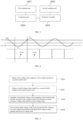
- FIG. 5 shows a control method of a bi-directional DC/DC converter in some embodiments of this application, which is used in a main control module of the bi-directional DC/DC converter in any of the above embodiments.
- the control method of a bi-directional DC/DC converter includes the following steps:
- the first voltage value may be obtained as follows: a first sampling unit samples a voltage at a corresponding node and conducts an A/D conversion.
- the second voltage value may be obtained as follows: a second sampling unit samples a voltage at an output node of the second rectifier module and conducts an A/D conversion.
- step S203 a formula obtained through inference in the above embodiments may be used to calculate the theoretical voltage control quantity.
- a theoretical voltage control quantity in the current control cycle that makes a voltage tracking error of the bi-directional DC/DC converter in the next control cycle minimized or relatively small is calculated.
- U c1_off (k) is a theoretical voltage control quantity in the current control cycle
- C 1 is a capacitance value of a first capacitor
- the first rectifier module is connected with the second rectifier module sequentially through a first capacitor and a transformer.
- U 0 (k) is a second voltage value in the current control cycle
- U ref is a reference voltage value
- T s is a duration of the control cycle
- V in is a voltage value of a first direct current voltage
- C oss is a parasitic capacitance value of a first switching tube S1, a second switching tube S2, a third switching tube S3, and a fourth switching tube S4,
- R L is a resistance value of an output load resistance of the second rectifier module 102.
- the first switching tube S1 and the third switching tube S3 form the first bridge arm
- the second switching tube S2 and the fourth switching tube S4 form a second bridge arm.
- step S03 may include the following sub-steps: S1031, obtaining a first relation between a voltage control quantity of the current control cycle and a voltage control quantity of the next control cycle; S1032, setting an evaluation function of a tracking error based on the preset reference voltage and a voltage control quantity of the next control cycle; and S1033, calculating the theoretical voltage control quantity of the bi-directional DC/DC converter in the current control cycle based on a preset reference voltage value, the second voltage value, the first relation, and the evaluation function.
- J opt is minimum, a minimum tracking error is obtained.
- a preset calculation formula may be obtained based on the first relation and the evaluation function; and then the theoretical voltage control quantity that makes a voltage tracking error of the bi-directional DC/DC converter in the next control cycle minimized may be calculated based on the preset calculation formula, the second voltage value, and the preset reference voltage.
- step S204 an output switching signal is used to regulate switch-on and switch-off of each switching tube of the first rectifier module, so as to achieve a purpose of regulating an actual output voltage in the next control cycle.
- step S204 may include: generating a switching signal based on the theoretical voltage control quantity and the first voltage value to control an actual output voltage of the bi-directional DC/DC converter in the next control cycle.
- the switching signal may be a single signal or a plurality of signals, thus controlling switch-on/switch-off of each switching tube of the first rectifier module.
- the step of generating a switching signal based on the theoretical voltage control quantity and the first voltage value includes: comparing the theoretical voltage control quantity with the first voltage value to generate the switching signal, where the switching signal is used to be sent to a control terminal of the first rectifier module to control a first voltage value output by the first rectifier module in the next control cycle, and further to control an actual output voltage of the bi-directional DC/DC converter in the next control cycle.
- the control signal includes a first control signal and a second control signal.
- Step S204 is specifically as follows: comparing the voltage control quantity with the first voltage value to obtain a first switching signal and a second switching signal in the next control cycle.
- the first switching signal is used to control switch-on and switch-off of an upper bridge arm of the first bridge arm and a lower bridge arm of the second bridge arm
- the second switching signal is used to control switch-on and switch-off of a lower bridge arm of the first bridge arm and an upper bridge arm of the second bridge arm.
- the upper bridge arm of the first bridge arm is a first switching tube
- the lower bridge arm of the first bridge arm is a third switching tube
- the upper bridge arm of the second bridge arm is a second switching tube
- the lower bridge arm of the second bridge arm is a fourth switching tube.
- the upper arm of the first bridge arm and the lower arm of the second bridge arm are switched on, and the lower arm of the first bridge arm and the upper arm of the second bridge arm are switched off.
- the first voltage value is in a second interval in the current control cycle, in the next control cycle, the upper bridge arm of the first bridge arm and the lower bridge arm of the second bridge arm are switched off, and the lower bridge arm of the first bridge arm and the upper bridge arm of the second bridge arm are switched on.
- the first voltage value includes a valley value V 11 and a peak value V 22 in each control cycle.
- the first interval is a union set of (-U c1_off , V l1 ] and [V l1 , U c1_off ); and the second interval is a union set of [V 22 , -U c1_off ) and (U c1_off , V 22 ], and U c1_off is a theoretical voltage control quantity.
- a first voltage value output by a first rectifier module in the current control cycle is obtained; a second voltage value output by a second rectifier module in the current control cycle is obtained, where a source terminal transmits electric energy to the destination terminal sequentially through the first rectifier module and the second rectifier module; a theoretical voltage control quantity of the bi-directional DC/DC converter in the current control cycle is calculated based on a preset reference voltage value and the second voltage value; and an actual output voltage of the bi-directional DC/DC converter in a next control cycle is set based on the theoretical voltage control quantity and the first voltage value, so that a beneficial effect of reducing a voltage tracking error in the next control cycle is achieved, and an extremely fast dynamic response may be received in all working conditions.
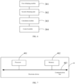
- FIG. 6 is a structural diagram of a control apparatus of a bi-directional DC/DC converter in some embodiments of this application.
- the apparatus includes a first obtaining module 301, a second obtaining module 302, a calculation module 303, and a control module 304.
- the first obtaining module 301 is configured to obtain a first voltage value output by a first rectifier module in the current control cycle; and the first voltage value may be obtained as follows: a first sampling unit samples a voltage at a corresponding node and conducts an A/D conversion.
- the second obtaining module 302 is configured to obtain a second voltage value output by a second rectifier module in the current control cycle.
- a source terminal transmits electric energy to a destination terminal sequentially through the first rectifier module and the second rectifier module.
- the second voltage value may be obtained as follows: a second sampling unit samples a voltage at an output node of the second rectifier module and conducts an A/D conversion
- the calculation module 303 is configured to calculate a theoretical voltage control quantity of the bi-directional DC/DC converter in the current control cycle based on a preset reference voltage value and the second voltage value, to reduce a voltage tracking error in the next control cycle.
- a theoretical voltage control quantity in the current control cycle that makes a voltage tracking error of the bi-directional DC/DC converter in the next control cycle minimized or relatively small is calculated.
- U c1_off (k) is a theoretical voltage control quantity in the current control cycle
- C 1 is a capacitance value of a first capacitor
- the first rectifier module is connected with the second rectifier module sequentially through a first capacitor and a transformer.
- U 0 (k) is a second voltage value in the current control cycle
- U ref is a reference voltage value
- T s is a duration of the control cycle
- V in is a voltage value of a first direct current voltage
- C oss is a parasitic capacitance value of a first switching tube S1, a second switching tube S2, a third switching tube S3, and a fourth switching tube S4,
- R L is a resistance value of an output load resistance of the second rectifier module 102.
- the first switching tube S1 and the third switching tube S3 form the first bridge arm
- the second switching tube S2 and the fourth switching tube S4 form a second bridge arm.
- the control module 304 is configured to set an actual output voltage of the bi-directional DC/DC converter in the next control cycle based on the theoretical voltage control quantity and the first voltage value.
- An output switching signal is used to regulate switch-on and switch-off of each switching tube of the first rectifier module, so as to achieve a purpose of regulating an actual output voltage in the next control cycle.
- control module 304 is configured to generate a switching signal based on the theoretical voltage control quantity and the first voltage value to control an actual output voltage of the bi-directional DC/DC converter in the next control cycle.
- the switching signal may be a single signal or a plurality of signals, thus controlling switch-on/switch-off of each switching tube of the first rectifier module.
- the step of generating a switching signal based on the theoretical voltage control quantity and the first voltage value includes: comparing the theoretical voltage control quantity with the first voltage value to generate the switching signal, where the switching signal is used to be sent to a control terminal of the first rectifier module to control a first voltage value output by the first rectifier module in the next control cycle, and further to control an actual output voltage of the bi-directional DC/DC converter in the next control cycle.
- the control signal includes a first control signal and a second control signal.
- the control module 304 is configured to compare the voltage control quantity with the first voltage value to obtain a first switching signal and a second switching signal in the next control cycle.
- the first switching signal is used to control switch-on and switch-off of an upper bridge arm of the first bridge arm and a lower bridge arm of the second bridge arm
- the second switching signal is used to control switch-on and switch-off of a lower bridge arm of the first bridge arm and an upper bridge arm of the second bridge arm.
- the upper bridge arm of the first bridge arm is a first switching tube
- the lower bridge arm of the first bridge arm is a third switching tube
- the upper bridge arm of the second bridge arm is a second switching tube
- the lower bridge arm of the second bridge arm is a fourth switching tube.
- the upper arm of the first bridge arm and the lower arm of the second bridge arm are switched on, and the lower arm of the first bridge arm and the upper arm of the second bridge arm are switched off.
- the first voltage value is in a second interval in the current control cycle, in the next control cycle, the upper bridge arm of the first bridge arm and the lower bridge arm of the second bridge arm are switched off, and the lower bridge arm of the first bridge arm and the upper bridge arm of the second bridge arm are switched on.
- the first voltage value includes a valley value V 11 and a peak value V 22 in each control cycle.
- the first interval is a union set of (-U c1_off , V l1 ] and [V l1 , U c1_off ); and the second interval is a union set of [V 22 , U cl_off ) and (U c1_off , V 22 ], and U cl_off is a theoretical voltage control quantity.
- a first voltage value output by a first rectifier module in the current control cycle is obtained; a second voltage value output by a second rectifier module in the current control cycle is obtained, where a source terminal transmits electric energy to a destination terminal sequentially through the first rectifier module and the second rectifier module; a theoretical voltage control quantity of the bi-directional DC/DC converter in the current control cycle is calculated based on a preset reference voltage value and the second voltage value; and an actual output voltage of the bi-directional DC/DC converter in a next control cycle is set based on the theoretical voltage control quantity and the first voltage value, so that a beneficial effect of reducing the voltage tracking error in the next control cycle is achieved, and an extremely fast dynamic response may be received in all working conditions.
- FIG. 7 is a structural schematic diagram of an electronic device provided in the embodiments of this application.
- This application provides an electronic device 4, including: a processor 401 and a memory 402.
- the processor 401 and the memory 402 are interconnected and communicated with each other through a communication bus 403 and/or another form of connection mechanism (not shown).
- the memory 402 stores a computer program executable on the processor 401.
- the processor 401 executes the computer program so as to implement the method in any of the optional implementations in the above embodiments.
- the embodiments of this application provide a storage medium.
- the storage medium may be any type of volatile or non-volatile storage device or a combination thereof such as a static random access memory (S some embodimentstatic Random Access Memory, SRAM for short), an electrically erasable programmable read-only memory (Electrically Erasable Programmable Read-Only Memory, EEPROM for short), an erasable programmable read only memory (Erasable Programmable Read Only Memory, EPROM for short), a programmable read-only memory (Programmable Red-Only Memory, PROM for short), a read-only memory (Read-Only Memory, ROM for short), a magnetic memory, a flash memory, a magnetic disk or a compact disk.
- SRAM static random access memory
- SRAM static random access memory
- EEPROM Electrically erasable programmable read-only memory
- EPROM Erasable Programmable Read Only Memory
- PROM programmable read-only memory
- PROM Read-Only Memory
Landscapes
- Engineering & Computer Science (AREA)
- Power Engineering (AREA)
- Transportation (AREA)
- Mechanical Engineering (AREA)
- Dc-Dc Converters (AREA)
- Signal Processing For Digital Recording And Reproducing (AREA)
Claims (11)
- Steuerverfahren für einen bidirektionalen DC/DC-Wandler (100), wobei ein Quellenanschluss (200) durch ein erstes Gleichrichtermodul (101) und ein zweites Gleichrichtermodul (102) des bidirektionalen DC/DC-Wandlers (100) sequentiell elektrische Energie zu einem Zielanschluss überträgt, wobei das erste Gleichrichtermodul (101) konfiguriert ist, um einen ersten Gleichstrom zu erhalten, der von dem Quellenanschluss (200) eingegeben wird, und um den ersten Gleichstrom in einen ersten Wechselstrom zu wandeln, der zu einem Transformator (104) durch einen ersten Kondensator (C1) und nachdem ein Spannungsanstieg oder -abfall des ersten Wechselstroms durch das zweite Gleichrichtermodul (102) gleichgerichtet wird, um einen entsprechenden zweiten Gleichstrom an den Zielanschluss auszugeben, übertragen wird,
und wobei das Verfahren Folgendes umfasst:Erhalten eines ersten Spannungswerts, der von einem ersten Gleichrichtermodul (101) in einem aktuellen Steuerzyklus ausgegeben wird;Erhalten eines zweiten Spannungswerts, der von einem zweiten Gleichrichtermodul (102) in dem aktuellen Steuerzyklus ausgegeben wird;Berechnen einer theoretischen Spannungssteuermenge des bidirektionalen DC/DC-Wandlers (100) in dem aktuellen Steuerzyklus basierend auf einem vorab festgelegten Referenzspannungswert und dem zweiten Spannungswert; undFestlegen einer tatsächlichen Ausgangsspannung des bidirektionalen DC/DC-Wandlers (100) in einem nächsten Steuerzyklus basierend auf der theoretischen Spannungssteuermenge und dem ersten Spannungswert;wobei das erste Gleichrichtermodul (101) einen ersten Brückenarm und einen zweiten Brückenarm umfasst; unddas Festlegen eines tatsächlichen Ausgabewerts des bidirektionalen DC/DC-Wandlers (100) in einem nächsten Steuerzyklus basierend auf der theoretischen Spannungssteuermenge und dem ersten Spannungswert Folgendes umfasst:Vergleichen der theoretischen Spannungssteuermenge mit dem ersten Spannungswert, um ein erstes Schaltsignal und ein zweites Schaltsignal in dem nächsten Steuerzyklus zu erhalten, wobei das erste Schaltsignal verwendet wird, um das Einschalten und Ausschalten eines oberen Brückenarms des ersten Brückenarms und eines unteren Brückenarms des zweiten Brückenarms zu steuern, und das zweite Schaltsignal verwendet wird, um das Einschalten und Ausschalten eines unteren Brückenarms des ersten Brückenarms und eines oberen Brückenarms des zweiten Brückenarms zu steuern;wobei das Berechnen einer theoretischen Spannungssteuermenge des bidirektionalen DC/DC-Wandlers (100) in dem aktuellen Steuerzyklus basierend auf einem vorab festgelegten Referenzspannungswert und dem zweiten Spannungswert Folgendes umfasst:Berechnen, gemäß der Formel Uc1_off(k) = [C1U0(k) Uref - C1U0 2(k) * (1 - Ts/RLC1) - 4Coss Vin 2]/(4C1 Vin), einer theoretischen Spannungssteuermenge, die einen Spannungsverfolgungsfehler des bidirektionalen DC/DC-Wandlers (100) in dem nächsten Steuerzyklus minimiert, wobeiUc1_off(k) eine theoretische Spannungssteuermenge in dem aktuellen Steuerzyklus ist, C1 ein Kapazitätswert des ersten Kondensators (C1) ist, U0(k) ein zweiter Spannungswert in dem aktuellen Steuerzyklus ist, Uref ein Referenzspannungswert ist, Ts eine Dauer des Steuerzyklus ist, Vin ein erster Spannungswert ist, Coss ein parasitärer Kapazitätswert einer ersten Schaltröhre (S1), einer zweiten Schaltröhre (S2), einer dritten Schaltröhre (S3) und einer vierten Schaltröhre (S4) ist, RL ein Widerstandswert eines Ausgangslastwiderstands des zweiten Gleichrichtermoduls (102) ist; und die zweite Schaltröhre (S2) und die dritte Schaltröhre (S3) den ersten Brückenarm bilden, und die erste Schaltröhre (S1) und die vierte Schaltröhre (S4) einen zweiten Brückenarm bilden. - Verfahren nach Anspruch 1, wobei das Festlegen einer tatsächlichen Ausgangsspannung des bidirektionalen DC/DC-Wandlers (100) in einem nächsten Steuerzyklus basierend auf der theoretischen Spannungssteuermenge und dem ersten Spannungswert Folgendes umfasst:
Erzeugen eines Schaltsignals basierend auf der theoretischen Spannungssteuermenge und dem ersten Spannungswert, um eine tatsächliche Ausgangsspannung des bidirektionalen DC/DC-Wandlers (100) in dem nächsten Steuerzyklus zu steuern. - Verfahren nach Anspruch 2, wobei das Erzeugen eines Schaltsignals basierend auf der theoretischen Spannungssteuermenge und dem ersten Spannungswert Folgendes umfasst:
Vergleichen der theoretischen Spannungssteuermenge mit dem ersten Spannungswert, um das Schaltsignal zu erzeugen, wobei das Schaltsignal verwendet wird, um zu einem Steueranschluss des ersten Gleichrichtermoduls (101) gesendet zu werden, um einen ersten Spannungswert, der von dem ersten Gleichrichtermodul (101) ausgegeben wird, in dem nächsten Steuerzyklus zu regeln, und ferner eine tatsächliche Ausgangsspannung des bidirektionalen DC/DC-Wandlers (100) in dem nächsten Steuerzyklus zu steuern. - Verfahren nach Anspruch 1, wobei das Festlegen einer tatsächlichen Ausgangsspannung des bidirektionalen DC/DC-Wandlers (100) in einem nächsten Steuerzyklus basierend auf der theoretischen Spannungssteuermenge und dem ersten Spannungswert Folgendes umfasst:
Ausgeben der theoretischen Spannungssteuermenge und des ersten Spannungswerts an einen Hysterese-Vergleicher zum Vergleich, um ein Schaltsignal zu erzeugen, wobei das Schaltsignal verwendet wird, um an einen Steueranschluss des ersten Gleichrichtermoduls (101) gesendet zu werden, um einen ersten Spannungswert, der von dem ersten Gleichrichtermodul (101) ausgegeben wird, in dem nächsten Steuerzyklus zu regeln, und ferner, um eine tatsächliche Ausgangsspannung des bidirektionalen DC/DC-Wandlers (100) in dem nächsten Steuerzyklus zu steuern. - Verfahren nach Anspruch 1, wobei, wenn der erste Spannungswert in einem ersten Intervall in dem aktuellen Steuerzyklus liegt, in dem nächsten Steuerzyklus der oberer Arm des ersten Brückenarms und der untere Arm des zweiten Brückenarms eingeschaltet werden und der untere Arm des ersten Brückenarms und der obere Arm des zweiten Brückenarms ausgeschaltet werden; undwenn der erste Spannungswert in einem zweiten Intervall in dem aktuellen Steuerzyklus liegt, in dem nächsten Steuerzyklus der obere Brückenarm des ersten Brückenarms und der untere Brückenarm des zweiten Brückenarms ausgeschaltet werden und der untere Brückenarm des ersten Brückenarms und der obere Brückenarm des zweiten Brückenarms eingeschaltet werden;wobei optional der erste Spannungswert einen Talwert V11 und einen Spitzenwert V22 in jedem Steuerzyklus umfasst;das erste Intervall eine Vereinigungsmenge von (-Uc1_off, V11] und [V11, Uc1_off) ist; unddas zweite Intervall eine Vereinigungsmenge von [V22, -Uc1_off) und (Uc1_off, V22] ist und Uc1_off eine theoretische Spannungssteuermenge ist.
- Bidirektionaler DC/DC-Wandler (100), umfassend:ein erstes Gleichrichtermodul (101), das konfiguriert ist, um einen ersten Gleichstrom in einen ersten Wechselstrom zur Ausgabe zu wandeln;einen Transformator (104), dessen Primärseite mit dem ersten Gleichrichtermodul (101) durch einen ersten Kondensator (C1) verbunden ist, um den ersten Wechselstrom zu erhalten, und dessen Sekundärseite einen zweiten Wechselstrom ausgibt;ein zweites Gleichrichtermodul (102), das konfiguriert ist, um mit der Sekundärseite verbunden zu werden, um den zweiten Wechselstrom gleichzurichten und um einen zweiten Gleichstrom auszugeben, der durch Gleichrichten erhalten wird; undwobei das erste Gleichrichtermodul (101) einen ersten Brückenarm und einen zweiten Brückenarm umfasst;wobei der erste Brückenarm eine erste Schaltröhre (S1) und eine dritte Schaltröhre (S3) umfasst;wobei der zweite Brückenarm eine zweite Schaltröhre (S2) und eine vierte Schaltröhre (S4) umfasst;wobei ein Eingangsanschluss der ersten Schaltröhre (S1) und ein Eingangsanschluss der zweiten Schaltröhre (S2) zum Verbinden einer positiven Elektrode eines Quellenanschlusses (200) verbunden sind; ein Ausgangsanschluss der dritten Schaltröhre (S3) und ein Ausgangsanschluss der vierten Schaltröhre (S4) zum Verbinden einer negativen Elektrode des Quellenanschlusses (200) verbunden sind; ein Ausgangsanschluss der ersten Schaltröhre (S1) und ein Eingangsanschluss der dritten Schaltröhre (S3) verbunden sind und dann mit einem positiven Anschluss auf einer Primärseite des Transformators (104) durch den ersten Kondensator (C1) verbunden werden; und ein Ausgangsanschluss der zweiten Schaltröhre (S2) und ein Eingangsanschluss der vierten Schaltröhre (S4) verbunden sind und dann mit einem negativen Anschluss auf der Primärseite des Transformators (104) verbunden werden; undwobei der bidirektionale DC/DC-Wandler ein Hauptsteuermodul (105) umfasst, das die Merkmale von Anspruch 10 umfasst.
- Bidirektionaler DC/DC-Wandler (100) nach Anspruch 6, wobei das Hauptsteuermodul (105) Folgendes umfasst:eine erste Abtasteinheit (1051), die konfiguriert ist, um mit dem ersten Kondensator (C1) und dem ersten Gleichrichtermodul (101) verbunden zu werden, um einen ersten Spannungswert zu erhalten;eine zweite Abtasteinheit (1052), die konfiguriert ist, um mit dem Ausgangsanschluss des zweiten Gleichrichtermoduls (102) verbunden zu werden, um einen zweiten Spannungswert zu erhalten;eine prädiktive Steuerung (1053), die konfiguriert ist, um mit der zweiten Abtasteinheit (1052) verbunden zu werden, um die theoretische Spannungssteuermenge in dem aktuellen Steuerzyklus basierend auf dem Referenzspannungswert und dem zweiten Spannungswert zu berechnen, um den Spannungsverfolgungsfehler in dem nächsten Steuerzyklus zu reduzieren; undeine Vergleichereinheit (1054), die konfiguriert ist, um mit der ersten Abtasteinheit (1051) und der prädiktiven Steuerung (1053) verbunden zu werden, um die theoretische Spannungssteuermenge mit dem ersten Spannungswert zu vergleichen, ein Schaltsignal basierend auf dem Vergleichsergebnis zu erzeugen und das Schaltsignal an einen Steueranschluss des ersten Gleichrichtermoduls (101) zu senden;wobei optional die Vergleichereinheit (1054) ein Hysterese-Vergleicher ist.
- Bidirektionaler DC/DC-Wandler (100) nach Anspruch 6, wobei, wenn der erste Spannungswert in einem ersten Intervall in dem aktuellen Steuerzyklus liegt, in dem nächsten Steuerzyklus die erste Schaltröhre (S1) und die vierte Schaltröhre (S4) eingeschaltet werden und die zweite Schaltröhre (S2) und die dritte Schaltröhre (S3) ausgeschaltet werden; und
wenn der erste Spannungswert in einem zweiten Intervall in dem aktuellen Steuerzyklus liegt, in dem nächsten Steuerzyklus die erste Schaltröhre (S1) und die vierte Schaltröhre (S4) ausgeschaltet werden und die zweite Schaltröhre (S2) und die dritte Schaltröhre (S3) eingeschaltet werden. - Bidirektionaler DC/DC-Wandler nach Anspruch 8, wobei der erste Spannungswert einen Talwert V11 und einen Spitzenwert V22 in jedem Steuerzyklus umfasst und das erste Intervall eine Vereinigungsmenge von (-Uc1_off, V11] und [V11, Uc1_off) ist; und
das zweite Intervall eine Vereinigungsmenge von [V22, -Uc1_off) und (Uc1_off, V22] ist und Uc1_off eine theoretische Spannungssteuermenge ist. - Steuervorrichtung für einen bidirektionalen DC/DC-Wandler (100), wobei ein Quellenanschluss (200) durch ein erstes Gleichrichtermodul (101) und ein zweites Gleichrichtermodul (102) des bidirektionalen DC/DC-Wandlers (100) elektrische Energie zu einem Zielanschluss überträgt, und wobei die Vorrichtung Folgendes umfasst:ein erstes Erhaltungsmodul (301), das konfiguriert ist, um einen ersten Spannungswert, der von einem ersten Gleichrichtermodul (101) ausgegeben wird, in einem aktuellen Steuerzyklus zu erhalten;ein zweites Erhaltungsmodul (302), das konfiguriert ist, um einen zweiten Spannungswert, der von einem zweiten Gleichrichtermodul (102) ausgegeben wird, in dem aktuellen Steuerzyklus zu erhalten;ein Berechnungsmodul (303), das konfiguriert ist, um eine theoretische Spannungssteuermenge des bidirektionalen DC/DC-Wandlers (100) in dem aktuellen Steuerzyklus basierend auf einem vorab festgelegten Referenzspannungswert und dem zweiten Spannungswert zu berechnen, um einen Spannungsverfolgungsfehler in einem nächsten Steuerzyklus zu reduzieren; undein Steuermodul (304), das konfiguriert ist, um ein Verfahren nach einem der Ansprüche 1 bis 5 auszuführen und dadurch eine tatsächliche Ausgangsspannung des bidirektionalen DC/DC-Wandlers (100) in dem nächsten Steuerzyklus basierend auf der theoretischen Spannungssteuermenge und dem ersten Spannungswert festzulegen.
- Speichermedium, wobei das Speichermedium ein Computerprogramm speichert, und wenn das Computerprogramm von einem Prozessor (401) ausgeführt wird, das Verfahren nach einem der Ansprüche 1 bis 5 implementiert wird.
Applications Claiming Priority (2)
| Application Number | Priority Date | Filing Date | Title |
|---|---|---|---|
| CN202110283689.3A CN115085553B (zh) | 2021-03-16 | 2021-03-16 | 双向dc/dc变换器及其控制方法、装置、存储介质 |
| PCT/CN2021/139739 WO2022193765A1 (zh) | 2021-03-16 | 2021-12-20 | 双向dc/dc变换器及其控制方法、装置、存储介质 |
Publications (3)
| Publication Number | Publication Date |
|---|---|
| EP4092897A1 EP4092897A1 (de) | 2022-11-23 |
| EP4092897A4 EP4092897A4 (de) | 2023-08-16 |
| EP4092897B1 true EP4092897B1 (de) | 2024-03-06 |
Family
ID=83246135
Family Applications (1)
| Application Number | Title | Priority Date | Filing Date |
|---|---|---|---|
| EP21921637.1A Active EP4092897B1 (de) | 2021-03-16 | 2021-12-20 | Bidirektionaler gleichstromwandler und steuerungsverfahren dafür sowie vorrichtung dafür und speichermedium |
Country Status (8)
| Country | Link |
|---|---|
| US (1) | US12126247B2 (de) |
| EP (1) | EP4092897B1 (de) |
| JP (1) | JP7446429B2 (de) |
| KR (1) | KR102760676B1 (de) |
| CN (1) | CN115085553B (de) |
| ES (1) | ES2980793T3 (de) |
| HU (1) | HUE066524T2 (de) |
| WO (1) | WO2022193765A1 (de) |
Families Citing this family (1)
| Publication number | Priority date | Publication date | Assignee | Title |
|---|---|---|---|---|
| CN118330311B (zh) * | 2024-06-13 | 2024-09-06 | 中国电力科学研究院有限公司 | 一种三相多功能标准谐波电能表及三相谐波电能测量方法 |
Family Cites Families (23)
| Publication number | Priority date | Publication date | Assignee | Title |
|---|---|---|---|---|
| TWI340528B (en) * | 2007-04-03 | 2011-04-11 | Delta Electronics Inc | Resonant converter system and controlling method thereof having relatively better efficiency |
| CN101976965B (zh) * | 2010-10-08 | 2013-04-03 | 江苏博纬新能源科技有限公司 | 直流跟踪控制的大功率光伏并网逆变器 |
| CN204068709U (zh) * | 2014-07-10 | 2014-12-31 | 西南交通大学 | 移相全桥dc-dc变换器的离散移相角控制装置 |
| US20160181925A1 (en) * | 2014-12-17 | 2016-06-23 | National Chung Shan Institute Of Science And Technology | Bidirectional dc-dc converter |
| CN204615654U (zh) * | 2015-05-12 | 2015-09-02 | 江苏固德威电源科技有限公司 | 谐振电路及采用其的双向储能逆变器 |
| CN105871215A (zh) * | 2016-05-17 | 2016-08-17 | 华南理工大学 | 用于双向clllc谐振变换器的整流控制电路 |
| JP6390823B2 (ja) * | 2016-06-06 | 2018-09-19 | 株式会社村田製作所 | スイッチング電源装置 |
| CN106533204B (zh) * | 2016-10-19 | 2019-11-12 | 南京博兰得电子科技有限公司 | 谐振式交流直流变换装置及其控制方法 |
| US10277140B2 (en) * | 2017-08-31 | 2019-04-30 | Google Llc | High-bandwith resonant power converters |
| JP2020532943A (ja) * | 2017-09-05 | 2020-11-12 | ザ ガバニング カウンシル オブ ザ ユニバーシティ オブ トロントThe Governing Council Of The University Of Toronto | 電気自動車パワーハブおよびその動作モード |
| JP6948918B2 (ja) * | 2017-11-10 | 2021-10-13 | 株式会社Soken | 電力変換装置の制御装置 |
| CN109039083B (zh) * | 2018-07-20 | 2020-06-30 | 清华大学 | 谐振型隔离双向直流变换器的瞬态功率平衡方法及系统 |
| CN109586580B (zh) | 2018-12-12 | 2020-09-15 | 矽力杰半导体技术(杭州)有限公司 | 控制电路、谐振变换器及集成电路控制芯片 |
| US10763756B2 (en) * | 2018-12-13 | 2020-09-01 | Power Integrations, Inc. | Apparatus and methods for sensing resonant circuit signals to enhance control in a resonant converter |
| JP2020108260A (ja) * | 2018-12-27 | 2020-07-09 | パナソニックIpマネジメント株式会社 | 充電装置、及び車両 |
| JP6988839B2 (ja) * | 2019-02-01 | 2022-01-05 | オムロン株式会社 | 共振型コンバータ制御回路とその制御方法及び共振型コンバータ |
| US11437917B2 (en) * | 2019-07-25 | 2022-09-06 | Texas Instruments Incorporated | Predictive synchronous rectifier sensing and control |
| KR102691476B1 (ko) * | 2019-08-21 | 2024-08-01 | 현대자동차주식회사 | 차량용 배터리 승온 시스템 |
| CN110838793B (zh) * | 2019-10-21 | 2021-07-20 | 浙江大学 | 一种应用于双向cllc谐振变换器的同步整流电路及控制策略 |
| CN110855149B (zh) * | 2019-11-22 | 2021-10-01 | 哈尔滨工程大学 | 一种直流变换器预测控制方法 |
| KR102177142B1 (ko) * | 2020-01-09 | 2020-11-10 | 주식회사 효성 | 절연형 양방향 dc-dc 컨버터에서 센서리스 과전류 예측방법 |
| CN112087063B (zh) * | 2020-03-25 | 2022-04-08 | 中国矿业大学 | 一种无线电能传输系统的改进型自抗扰控制方法及系统 |
| CN112187058B (zh) * | 2020-09-17 | 2022-02-22 | 北京智芯微电子科技有限公司 | Dab变流器的鲁棒稳定控制方法及装置 |
-
2021
- 2021-03-16 CN CN202110283689.3A patent/CN115085553B/zh active Active
- 2021-12-20 EP EP21921637.1A patent/EP4092897B1/de active Active
- 2021-12-20 HU HUE21921637A patent/HUE066524T2/hu unknown
- 2021-12-20 JP JP2022534291A patent/JP7446429B2/ja active Active
- 2021-12-20 KR KR1020227018033A patent/KR102760676B1/ko active Active
- 2021-12-20 WO PCT/CN2021/139739 patent/WO2022193765A1/zh not_active Ceased
- 2021-12-20 ES ES21921637T patent/ES2980793T3/es active Active
-
2022
- 2022-08-09 US US17/884,561 patent/US12126247B2/en active Active
Also Published As
| Publication number | Publication date |
|---|---|
| ES2980793T3 (es) | 2024-10-03 |
| US12126247B2 (en) | 2024-10-22 |
| EP4092897A4 (de) | 2023-08-16 |
| JP2023522517A (ja) | 2023-05-31 |
| CN115085553A (zh) | 2022-09-20 |
| KR20220130094A (ko) | 2022-09-26 |
| EP4092897A1 (de) | 2022-11-23 |
| HUE066524T2 (hu) | 2024-08-28 |
| US20220385165A1 (en) | 2022-12-01 |
| JP7446429B2 (ja) | 2024-03-08 |
| WO2022193765A1 (zh) | 2022-09-22 |
| KR102760676B1 (ko) | 2025-02-03 |
| CN115085553B (zh) | 2023-12-22 |
Similar Documents
| Publication | Publication Date | Title |
|---|---|---|
| Rodriguez et al. | Different purpose design strategies and techniques to improve the performance of a dual active bridge with phase-shift control | |
| CN112600432B (zh) | 一种llc谐振变换器预测电荷控制方法 | |
| CN103001494B (zh) | 开关电源及控制其恒定输出电流的控制器 | |
| CN102904466B (zh) | 开关电源控制器 | |
| US12267014B2 (en) | Non-isolated DCDC resonant conversion control circuit and control method | |
| CN114389454B (zh) | 一种隔离电源的副边控制方法及副边控制系统 | |
| EP4092897B1 (de) | Bidirektionaler gleichstromwandler und steuerungsverfahren dafür sowie vorrichtung dafür und speichermedium | |
| Mammeri et al. | Modeling and control of a three-phase interleaved buck converter as a battery charger | |
| He et al. | Unified Two-Time-Scale Modeling and Hybrid ZVS Modulation of LCC–LCC Compensated IPT System With Wide Input Voltage Range | |
| Anitha et al. | Optimized control techniques for enhancing the buck converter performance in lithium-ion battery charging | |
| CN103248246B (zh) | 离线式ac-dc控制电路和包含该控制电路的转换电路 | |
| Migoni et al. | A mixed modeling approach for efficient simulation of PWM switching mode power supplies | |
| US20250192596A1 (en) | Charger control method and apparatus, and charger and vehicle | |
| Agarwal et al. | Large signal analysis of the LCC-type parallel resonant converter using discrete time domain modeling | |
| Adam et al. | A triple active bridge converter based on model predictive control for more electric aircraft applications | |
| CN115149811B (zh) | 反激变换器及其启动控制方法 | |
| CN117375157A (zh) | 一种基于双有源桥变换器三重移相的锂电池模型预测方法 | |
| Du et al. | PSM control technique for primary‐side regulating fly‐back converters | |
| Zeltser et al. | Modeling, analysis and simulation of" AC inductor" based converters | |
| US9673691B2 (en) | Energy balance controller of electronic power converter and energy balance control method | |
| Borkar et al. | Performance Analysis of Half-Bridge LC Resonant Converter for UPS Battery Charging Application | |
| CN114710044A (zh) | 反激变换器及其恒流控制方法 | |
| Yu et al. | Modeling and analysis of primary side regulated flyback converter with pulse frequency modulation | |
| Sidorov et al. | Input Source Identification Algorithm For Isolated Buck-Boost DC-DC Converter | |
| CN117492500B (zh) | 一种用于电池阻抗谱测量的激励电流发生电路及控制方法 |
Legal Events
| Date | Code | Title | Description |
|---|---|---|---|
| STAA | Information on the status of an ep patent application or granted ep patent |
Free format text: STATUS: UNKNOWN |
|
| STAA | Information on the status of an ep patent application or granted ep patent |
Free format text: STATUS: THE INTERNATIONAL PUBLICATION HAS BEEN MADE |
|
| PUAI | Public reference made under article 153(3) epc to a published international application that has entered the european phase |
Free format text: ORIGINAL CODE: 0009012 |
|
| STAA | Information on the status of an ep patent application or granted ep patent |
Free format text: STATUS: REQUEST FOR EXAMINATION WAS MADE |
|
| PUAB | Information related to the publication of an a document modified or deleted |
Free format text: ORIGINAL CODE: 0009199EPPU |
|
| PUAI | Public reference made under article 153(3) epc to a published international application that has entered the european phase |
Free format text: ORIGINAL CODE: 0009012 |
|
| 17P | Request for examination filed |
Effective date: 20220803 |
|
| AK | Designated contracting states |
Kind code of ref document: A1 Designated state(s): AL AT BE BG CH CY CZ DE DK EE ES FI FR GB GR HR HU IE IS IT LI LT LU LV MC MK MT NL NO PL PT RO RS SE SI SK SM TR |
|
| REG | Reference to a national code |
Ref country code: DE Ipc: H02M0003000000 Ref country code: DE Ref legal event code: R079 Ref document number: 602021010222 Country of ref document: DE Free format text: PREVIOUS MAIN CLASS: H02M0003335000 Ipc: H02M0003000000 |
|
| R17P | Request for examination filed (corrected) |
Effective date: 20220803 |
|
| A4 | Supplementary search report drawn up and despatched |
Effective date: 20230717 |
|
| RIC1 | Information provided on ipc code assigned before grant |
Ipc: H02J 7/00 20060101ALI20230711BHEP Ipc: B60L 53/24 20190101ALI20230711BHEP Ipc: B60L 53/10 20190101ALI20230711BHEP Ipc: H02M 3/335 20060101ALI20230711BHEP Ipc: H02M 3/00 20060101AFI20230711BHEP |
|
| GRAP | Despatch of communication of intention to grant a patent |
Free format text: ORIGINAL CODE: EPIDOSNIGR1 |
|
| STAA | Information on the status of an ep patent application or granted ep patent |
Free format text: STATUS: GRANT OF PATENT IS INTENDED |
|
| RIC1 | Information provided on ipc code assigned before grant |
Ipc: H02J 7/00 20060101ALI20230901BHEP Ipc: B60L 53/24 20190101ALI20230901BHEP Ipc: B60L 53/10 20190101ALI20230901BHEP Ipc: H02M 3/335 20060101ALI20230901BHEP Ipc: H02M 3/00 20060101AFI20230901BHEP |
|
| DAV | Request for validation of the european patent (deleted) | ||
| DAX | Request for extension of the european patent (deleted) | ||
| INTG | Intention to grant announced |
Effective date: 20231002 |
|
| GRAS | Grant fee paid |
Free format text: ORIGINAL CODE: EPIDOSNIGR3 |
|
| GRAA | (expected) grant |
Free format text: ORIGINAL CODE: 0009210 |
|
| STAA | Information on the status of an ep patent application or granted ep patent |
Free format text: STATUS: THE PATENT HAS BEEN GRANTED |
|
| AK | Designated contracting states |
Kind code of ref document: B1 Designated state(s): AL AT BE BG CH CY CZ DE DK EE ES FI FR GB GR HR HU IE IS IT LI LT LU LV MC MK MT NL NO PL PT RO RS SE SI SK SM TR |
|
| P01 | Opt-out of the competence of the unified patent court (upc) registered |
Effective date: 20240204 |
|
| REG | Reference to a national code |
Ref country code: CH Ref legal event code: EP |
|
| REG | Reference to a national code |
Ref country code: IE Ref legal event code: FG4D |
|
| REG | Reference to a national code |
Ref country code: DE Ref legal event code: R096 Ref document number: 602021010222 Country of ref document: DE |
|
| REG | Reference to a national code |
Ref country code: LT Ref legal event code: MG9D |
|
| PG25 | Lapsed in a contracting state [announced via postgrant information from national office to epo] |
Ref country code: LT Free format text: LAPSE BECAUSE OF FAILURE TO SUBMIT A TRANSLATION OF THE DESCRIPTION OR TO PAY THE FEE WITHIN THE PRESCRIBED TIME-LIMIT Effective date: 20240306 |
|
| REG | Reference to a national code |
Ref country code: NL Ref legal event code: MP Effective date: 20240306 |
|
| PG25 | Lapsed in a contracting state [announced via postgrant information from national office to epo] |
Ref country code: GR Free format text: LAPSE BECAUSE OF FAILURE TO SUBMIT A TRANSLATION OF THE DESCRIPTION OR TO PAY THE FEE WITHIN THE PRESCRIBED TIME-LIMIT Effective date: 20240607 |
|
| PG25 | Lapsed in a contracting state [announced via postgrant information from national office to epo] |
Ref country code: RS Free format text: LAPSE BECAUSE OF FAILURE TO SUBMIT A TRANSLATION OF THE DESCRIPTION OR TO PAY THE FEE WITHIN THE PRESCRIBED TIME-LIMIT Effective date: 20240606 Ref country code: HR Free format text: LAPSE BECAUSE OF FAILURE TO SUBMIT A TRANSLATION OF THE DESCRIPTION OR TO PAY THE FEE WITHIN THE PRESCRIBED TIME-LIMIT Effective date: 20240306 |
|
| PG25 | Lapsed in a contracting state [announced via postgrant information from national office to epo] |
Ref country code: RS Free format text: LAPSE BECAUSE OF FAILURE TO SUBMIT A TRANSLATION OF THE DESCRIPTION OR TO PAY THE FEE WITHIN THE PRESCRIBED TIME-LIMIT Effective date: 20240606 Ref country code: LT Free format text: LAPSE BECAUSE OF FAILURE TO SUBMIT A TRANSLATION OF THE DESCRIPTION OR TO PAY THE FEE WITHIN THE PRESCRIBED TIME-LIMIT Effective date: 20240306 Ref country code: HR Free format text: LAPSE BECAUSE OF FAILURE TO SUBMIT A TRANSLATION OF THE DESCRIPTION OR TO PAY THE FEE WITHIN THE PRESCRIBED TIME-LIMIT Effective date: 20240306 Ref country code: GR Free format text: LAPSE BECAUSE OF FAILURE TO SUBMIT A TRANSLATION OF THE DESCRIPTION OR TO PAY THE FEE WITHIN THE PRESCRIBED TIME-LIMIT Effective date: 20240607 Ref country code: FI Free format text: LAPSE BECAUSE OF FAILURE TO SUBMIT A TRANSLATION OF THE DESCRIPTION OR TO PAY THE FEE WITHIN THE PRESCRIBED TIME-LIMIT Effective date: 20240306 Ref country code: BG Free format text: LAPSE BECAUSE OF FAILURE TO SUBMIT A TRANSLATION OF THE DESCRIPTION OR TO PAY THE FEE WITHIN THE PRESCRIBED TIME-LIMIT Effective date: 20240306 |
|
| REG | Reference to a national code |
Ref country code: DE Ref legal event code: R081 Ref document number: 602021010222 Country of ref document: DE Owner name: CONTEMPORARY AMPEREX TECHNOLOGY (HONG KONG) LI, HK Free format text: FORMER OWNER: CONTEMPORARY AMPEREX TECHNOLOGY CO., LIMITED, NINGDE CITY, FUJIAN, CN |
|
| REG | Reference to a national code |
Ref country code: AT Ref legal event code: MK05 Ref document number: 1664515 Country of ref document: AT Kind code of ref document: T Effective date: 20240306 |
|
| REG | Reference to a national code |
Ref country code: HU Ref legal event code: AG4A Ref document number: E066524 Country of ref document: HU |
|
| PG25 | Lapsed in a contracting state [announced via postgrant information from national office to epo] |
Ref country code: SE Free format text: LAPSE BECAUSE OF FAILURE TO SUBMIT A TRANSLATION OF THE DESCRIPTION OR TO PAY THE FEE WITHIN THE PRESCRIBED TIME-LIMIT Effective date: 20240306 Ref country code: LV Free format text: LAPSE BECAUSE OF FAILURE TO SUBMIT A TRANSLATION OF THE DESCRIPTION OR TO PAY THE FEE WITHIN THE PRESCRIBED TIME-LIMIT Effective date: 20240306 |
|
| PG25 | Lapsed in a contracting state [announced via postgrant information from national office to epo] |
Ref country code: NL Free format text: LAPSE BECAUSE OF FAILURE TO SUBMIT A TRANSLATION OF THE DESCRIPTION OR TO PAY THE FEE WITHIN THE PRESCRIBED TIME-LIMIT Effective date: 20240306 |
|
| REG | Reference to a national code |
Ref country code: GB Ref legal event code: 732E Free format text: REGISTERED BETWEEN 20240829 AND 20240904 |
|
| REG | Reference to a national code |
Ref country code: HU Ref legal event code: GB9C Owner name: CONTEMPORARY AMPEREX TECHNOLOGY (HONG KONG) LIMITED, HK Free format text: FORMER OWNER(S): CONTEMPORARY AMPEREX TECHNOLOGY CO., LIMITED, CN Ref country code: HU Ref legal event code: FH1C Free format text: FORMER REPRESENTATIVE(S): DANUBIA SZABADALMI ES JOGI IRODA KFT., HU Representative=s name: DANUBIA SZABADALMI ES JOGI IRODA KFT., HU |
|
| PG25 | Lapsed in a contracting state [announced via postgrant information from national office to epo] |
Ref country code: NL Free format text: LAPSE BECAUSE OF FAILURE TO SUBMIT A TRANSLATION OF THE DESCRIPTION OR TO PAY THE FEE WITHIN THE PRESCRIBED TIME-LIMIT Effective date: 20240306 |
|
| RAP2 | Party data changed (patent owner data changed or rights of a patent transferred) |
Owner name: CONTEMPORARY AMPEREX TECHNOLOGY(HONG KONG) LIMITED |
|
| REG | Reference to a national code |
Ref country code: ES Ref legal event code: FG2A Ref document number: 2980793 Country of ref document: ES Kind code of ref document: T3 Effective date: 20241003 |
|
| PG25 | Lapsed in a contracting state [announced via postgrant information from national office to epo] |
Ref country code: IS Free format text: LAPSE BECAUSE OF FAILURE TO SUBMIT A TRANSLATION OF THE DESCRIPTION OR TO PAY THE FEE WITHIN THE PRESCRIBED TIME-LIMIT Effective date: 20240706 |
|
| PG25 | Lapsed in a contracting state [announced via postgrant information from national office to epo] |
Ref country code: SM Free format text: LAPSE BECAUSE OF FAILURE TO SUBMIT A TRANSLATION OF THE DESCRIPTION OR TO PAY THE FEE WITHIN THE PRESCRIBED TIME-LIMIT Effective date: 20240306 Ref country code: PT Free format text: LAPSE BECAUSE OF FAILURE TO SUBMIT A TRANSLATION OF THE DESCRIPTION OR TO PAY THE FEE WITHIN THE PRESCRIBED TIME-LIMIT Effective date: 20240708 |
|
| PG25 | Lapsed in a contracting state [announced via postgrant information from national office to epo] |
Ref country code: CZ Free format text: LAPSE BECAUSE OF FAILURE TO SUBMIT A TRANSLATION OF THE DESCRIPTION OR TO PAY THE FEE WITHIN THE PRESCRIBED TIME-LIMIT Effective date: 20240306 Ref country code: EE Free format text: LAPSE BECAUSE OF FAILURE TO SUBMIT A TRANSLATION OF THE DESCRIPTION OR TO PAY THE FEE WITHIN THE PRESCRIBED TIME-LIMIT Effective date: 20240306 |
|
| PG25 | Lapsed in a contracting state [announced via postgrant information from national office to epo] |
Ref country code: AT Free format text: LAPSE BECAUSE OF FAILURE TO SUBMIT A TRANSLATION OF THE DESCRIPTION OR TO PAY THE FEE WITHIN THE PRESCRIBED TIME-LIMIT Effective date: 20240306 |
|
| PG25 | Lapsed in a contracting state [announced via postgrant information from national office to epo] |
Ref country code: PL Free format text: LAPSE BECAUSE OF FAILURE TO SUBMIT A TRANSLATION OF THE DESCRIPTION OR TO PAY THE FEE WITHIN THE PRESCRIBED TIME-LIMIT Effective date: 20240306 |
|
| PG25 | Lapsed in a contracting state [announced via postgrant information from national office to epo] |
Ref country code: SK Free format text: LAPSE BECAUSE OF FAILURE TO SUBMIT A TRANSLATION OF THE DESCRIPTION OR TO PAY THE FEE WITHIN THE PRESCRIBED TIME-LIMIT Effective date: 20240306 |
|
| PG25 | Lapsed in a contracting state [announced via postgrant information from national office to epo] |
Ref country code: SM Free format text: LAPSE BECAUSE OF FAILURE TO SUBMIT A TRANSLATION OF THE DESCRIPTION OR TO PAY THE FEE WITHIN THE PRESCRIBED TIME-LIMIT Effective date: 20240306 Ref country code: SK Free format text: LAPSE BECAUSE OF FAILURE TO SUBMIT A TRANSLATION OF THE DESCRIPTION OR TO PAY THE FEE WITHIN THE PRESCRIBED TIME-LIMIT Effective date: 20240306 Ref country code: RO Free format text: LAPSE BECAUSE OF FAILURE TO SUBMIT A TRANSLATION OF THE DESCRIPTION OR TO PAY THE FEE WITHIN THE PRESCRIBED TIME-LIMIT Effective date: 20240306 Ref country code: PT Free format text: LAPSE BECAUSE OF FAILURE TO SUBMIT A TRANSLATION OF THE DESCRIPTION OR TO PAY THE FEE WITHIN THE PRESCRIBED TIME-LIMIT Effective date: 20240708 Ref country code: PL Free format text: LAPSE BECAUSE OF FAILURE TO SUBMIT A TRANSLATION OF THE DESCRIPTION OR TO PAY THE FEE WITHIN THE PRESCRIBED TIME-LIMIT Effective date: 20240306 Ref country code: IS Free format text: LAPSE BECAUSE OF FAILURE TO SUBMIT A TRANSLATION OF THE DESCRIPTION OR TO PAY THE FEE WITHIN THE PRESCRIBED TIME-LIMIT Effective date: 20240706 Ref country code: EE Free format text: LAPSE BECAUSE OF FAILURE TO SUBMIT A TRANSLATION OF THE DESCRIPTION OR TO PAY THE FEE WITHIN THE PRESCRIBED TIME-LIMIT Effective date: 20240306 Ref country code: CZ Free format text: LAPSE BECAUSE OF FAILURE TO SUBMIT A TRANSLATION OF THE DESCRIPTION OR TO PAY THE FEE WITHIN THE PRESCRIBED TIME-LIMIT Effective date: 20240306 Ref country code: AT Free format text: LAPSE BECAUSE OF FAILURE TO SUBMIT A TRANSLATION OF THE DESCRIPTION OR TO PAY THE FEE WITHIN THE PRESCRIBED TIME-LIMIT Effective date: 20240306 |
|
| PG25 | Lapsed in a contracting state [announced via postgrant information from national office to epo] |
Ref country code: IT Free format text: LAPSE BECAUSE OF FAILURE TO SUBMIT A TRANSLATION OF THE DESCRIPTION OR TO PAY THE FEE WITHIN THE PRESCRIBED TIME-LIMIT Effective date: 20240306 |
|
| REG | Reference to a national code |
Ref country code: DE Ref legal event code: R097 Ref document number: 602021010222 Country of ref document: DE |
|
| PG25 | Lapsed in a contracting state [announced via postgrant information from national office to epo] |
Ref country code: IT Free format text: LAPSE BECAUSE OF FAILURE TO SUBMIT A TRANSLATION OF THE DESCRIPTION OR TO PAY THE FEE WITHIN THE PRESCRIBED TIME-LIMIT Effective date: 20240306 |
|
| PLBE | No opposition filed within time limit |
Free format text: ORIGINAL CODE: 0009261 |
|
| STAA | Information on the status of an ep patent application or granted ep patent |
Free format text: STATUS: NO OPPOSITION FILED WITHIN TIME LIMIT |
|
| PG25 | Lapsed in a contracting state [announced via postgrant information from national office to epo] |
Ref country code: DK Free format text: LAPSE BECAUSE OF FAILURE TO SUBMIT A TRANSLATION OF THE DESCRIPTION OR TO PAY THE FEE WITHIN THE PRESCRIBED TIME-LIMIT Effective date: 20240306 |
|
| PG25 | Lapsed in a contracting state [announced via postgrant information from national office to epo] |
Ref country code: DK Free format text: LAPSE BECAUSE OF FAILURE TO SUBMIT A TRANSLATION OF THE DESCRIPTION OR TO PAY THE FEE WITHIN THE PRESCRIBED TIME-LIMIT Effective date: 20240306 |
|
| 26N | No opposition filed |
Effective date: 20241209 |
|
| PG25 | Lapsed in a contracting state [announced via postgrant information from national office to epo] |
Ref country code: SI Free format text: LAPSE BECAUSE OF FAILURE TO SUBMIT A TRANSLATION OF THE DESCRIPTION OR TO PAY THE FEE WITHIN THE PRESCRIBED TIME-LIMIT Effective date: 20240306 |
|
| PG25 | Lapsed in a contracting state [announced via postgrant information from national office to epo] |
Ref country code: MC Free format text: LAPSE BECAUSE OF FAILURE TO SUBMIT A TRANSLATION OF THE DESCRIPTION OR TO PAY THE FEE WITHIN THE PRESCRIBED TIME-LIMIT Effective date: 20240306 |
|
| REG | Reference to a national code |
Ref country code: CH Ref legal event code: PL |
|
| PG25 | Lapsed in a contracting state [announced via postgrant information from national office to epo] |
Ref country code: LU Free format text: LAPSE BECAUSE OF NON-PAYMENT OF DUE FEES Effective date: 20241220 |
|
| REG | Reference to a national code |
Ref country code: BE Ref legal event code: MM Effective date: 20241231 |
|
| PG25 | Lapsed in a contracting state [announced via postgrant information from national office to epo] |
Ref country code: BE Free format text: LAPSE BECAUSE OF NON-PAYMENT OF DUE FEES Effective date: 20241231 |
|
| PG25 | Lapsed in a contracting state [announced via postgrant information from national office to epo] |
Ref country code: CH Free format text: LAPSE BECAUSE OF NON-PAYMENT OF DUE FEES Effective date: 20241231 |
|
| PG25 | Lapsed in a contracting state [announced via postgrant information from national office to epo] |
Ref country code: IE Free format text: LAPSE BECAUSE OF NON-PAYMENT OF DUE FEES Effective date: 20241220 |
|
| PGFP | Annual fee paid to national office [announced via postgrant information from national office to epo] |
Ref country code: DE Payment date: 20251212 Year of fee payment: 5 |
|
| PGFP | Annual fee paid to national office [announced via postgrant information from national office to epo] |
Ref country code: GB Payment date: 20251211 Year of fee payment: 5 |
|
| PGFP | Annual fee paid to national office [announced via postgrant information from national office to epo] |
Ref country code: NO Payment date: 20251215 Year of fee payment: 5 |
|
| PGFP | Annual fee paid to national office [announced via postgrant information from national office to epo] |
Ref country code: HU Payment date: 20251209 Year of fee payment: 5 Ref country code: FR Payment date: 20251212 Year of fee payment: 5 |
|
| PGFP | Annual fee paid to national office [announced via postgrant information from national office to epo] |
Ref country code: ES Payment date: 20260105 Year of fee payment: 5 |