EP4092827B1 - Multiband antenna - Google Patents
Multiband antenna Download PDFInfo
- Publication number
- EP4092827B1 EP4092827B1 EP22167249.6A EP22167249A EP4092827B1 EP 4092827 B1 EP4092827 B1 EP 4092827B1 EP 22167249 A EP22167249 A EP 22167249A EP 4092827 B1 EP4092827 B1 EP 4092827B1
- Authority
- EP
- European Patent Office
- Prior art keywords
- multiband antenna
- edge
- slot
- ground terminal
- feeding
- Prior art date
- Legal status (The legal status is an assumption and is not a legal conclusion. Google has not performed a legal analysis and makes no representation as to the accuracy of the status listed.)
- Active
Links
Images




Classifications
-
- H—ELECTRICITY
- H01—ELECTRIC ELEMENTS
- H01Q—ANTENNAS, i.e. RADIO AERIALS
- H01Q1/00—Details of, or arrangements associated with, antennas
- H01Q1/50—Structural association of antennas with earthing switches, lead-in devices or lightning protectors
-
- H—ELECTRICITY
- H01—ELECTRIC ELEMENTS
- H01Q—ANTENNAS, i.e. RADIO AERIALS
- H01Q5/00—Arrangements for simultaneous operation of antennas on two or more different wavebands, e.g. dual-band or multi-band arrangements
- H01Q5/30—Arrangements for providing operation on different wavebands
- H01Q5/307—Individual or coupled radiating elements, each element being fed in an unspecified way
- H01Q5/342—Individual or coupled radiating elements, each element being fed in an unspecified way for different propagation modes
- H01Q5/357—Individual or coupled radiating elements, each element being fed in an unspecified way for different propagation modes using a single feed point
- H01Q5/364—Creating multiple current paths
-
- H—ELECTRICITY
- H01—ELECTRIC ELEMENTS
- H01Q—ANTENNAS, i.e. RADIO AERIALS
- H01Q1/00—Details of, or arrangements associated with, antennas
- H01Q1/36—Structural form of radiating elements, e.g. cone, spiral, umbrella; Particular materials used therewith
- H01Q1/38—Structural form of radiating elements, e.g. cone, spiral, umbrella; Particular materials used therewith formed by a conductive layer on an insulating support
-
- H—ELECTRICITY
- H01—ELECTRIC ELEMENTS
- H01Q—ANTENNAS, i.e. RADIO AERIALS
- H01Q21/00—Antenna arrays or systems
- H01Q21/06—Arrays of individually energised antenna units similarly polarised and spaced apart
- H01Q21/061—Two dimensional planar arrays
- H01Q21/064—Two dimensional planar arrays using horn or slot aerials
-
- H—ELECTRICITY
- H01—ELECTRIC ELEMENTS
- H01Q—ANTENNAS, i.e. RADIO AERIALS
- H01Q1/00—Details of, or arrangements associated with, antennas
- H01Q1/27—Adaptation for use in or on movable bodies
- H01Q1/28—Adaptation for use in or on aircraft, missiles, satellites, or balloons
- H01Q1/282—Modifying the aerodynamic properties of the vehicle, e.g. projecting type aerials
- H01Q1/283—Blade, stub antennas
-
- H—ELECTRICITY
- H01—ELECTRIC ELEMENTS
- H01Q—ANTENNAS, i.e. RADIO AERIALS
- H01Q1/00—Details of, or arrangements associated with, antennas
- H01Q1/36—Structural form of radiating elements, e.g. cone, spiral, umbrella; Particular materials used therewith
-
- H—ELECTRICITY
- H01—ELECTRIC ELEMENTS
- H01Q—ANTENNAS, i.e. RADIO AERIALS
- H01Q1/00—Details of, or arrangements associated with, antennas
- H01Q1/44—Details of, or arrangements associated with, antennas using equipment having another main function to serve additionally as an antenna, e.g. means for giving an antenna an aesthetic aspect
- H01Q1/46—Electric supply lines or communication lines
-
- H—ELECTRICITY
- H01—ELECTRIC ELEMENTS
- H01Q—ANTENNAS, i.e. RADIO AERIALS
- H01Q1/00—Details of, or arrangements associated with, antennas
- H01Q1/48—Earthing means; Earth screens; Counterpoises
-
- H—ELECTRICITY
- H01—ELECTRIC ELEMENTS
- H01Q—ANTENNAS, i.e. RADIO AERIALS
- H01Q5/00—Arrangements for simultaneous operation of antennas on two or more different wavebands, e.g. dual-band or multi-band arrangements
- H01Q5/20—Arrangements for simultaneous operation of antennas on two or more different wavebands, e.g. dual-band or multi-band arrangements characterised by the operating wavebands
- H01Q5/28—Arrangements for establishing polarisation or beam width over two or more different wavebands
-
- H—ELECTRICITY
- H01—ELECTRIC ELEMENTS
- H01Q—ANTENNAS, i.e. RADIO AERIALS
- H01Q5/00—Arrangements for simultaneous operation of antennas on two or more different wavebands, e.g. dual-band or multi-band arrangements
- H01Q5/30—Arrangements for providing operation on different wavebands
-
- H—ELECTRICITY
- H01—ELECTRIC ELEMENTS
- H01Q—ANTENNAS, i.e. RADIO AERIALS
- H01Q5/00—Arrangements for simultaneous operation of antennas on two or more different wavebands, e.g. dual-band or multi-band arrangements
- H01Q5/50—Feeding or matching arrangements for broad-band or multi-band operation
Definitions
- This invention relates to a multiband antenna, particularly to a multiband antenna provided with a conductor main portion formed with a slot.
- US 2018/123261 A1 discloses an antenna device including first and second split ring resonators and a power supply line.
- the first split ring resonator includes a conductor enclosing a first opening and having a first void separating a part of the conductor.
- the second split ring resonator is opposed to the first split ring resonator, including a conductor which encloses a second opening and has a second void separating a part of the conductor.
- the power supply line feeds power to the first or second split ring resonator.
- the first split ring resonator is not electrically connected to the second split ring resonator.
- the first void does not overlap with the second void in an opposing direction of the first split ring resonator and the second split ring resonator.
- US 2003/112198 A1 discloses an antenna that has at least one slotted planar element.
- the slot in the planar element is open at one end and configured such that the planar element has a quarter wave resonance mode at a first frequency and there is a second resonant frequency at which the element has a 3/4 wave resonance mode and/or the element's slot has a quarter wave resonance mode.
- the second frequency is not substantially three time the first frequency.
- US 2011/291895 A1 discloses a multi-band antenna including a conductive ground plane element, a conductive driven element having a feed point and a conductive coupling element located on at least one but not all sides of the conductive driven element and coupled to the conductive ground plane element and to the conductive driven element, wherein a resonant frequency associated with the conductive coupling element is independent of a size of the conductive ground plane element.
- Patent Document 1 JP 2012-85262 A (Patent Document 1) discloses an example of an antenna device provided with a conductive plate formed with a slot.
- an antenna device 90 disclosed in Patent Document 1 is provided with a conductive plate 910 provided on one surface of a dielectric substrate (not shown).
- the conductive plate 910 is formed with two slots 920 and 930.
- the slots 920 and 930 have open ends 922 and 932, respectively.
- the slots 920 and 930 are arranged so that the open ends 922 and 932 face each other.
- the open ends 922 and 932 are contiguous to an opening portion 940 which opens at an edge of the conductive plate 910.
- the antenna device 90 further has a stub 950.
- the stub 950 is formed on the other surface of the dielectric substrate (not shown).
- One end of the stub 950 is connected to the conductive plate 910 through a via 960.
- the stub 950 extends so as to intersect with the slot 920 when viewed in plane.
- the antenna device 90 of Patent Document 1 uses the conductive plate 910 formed on the surface of the dielectric substrate. Accordingly, the antenna device 90 has a problem that it is difficult to reduce a size thereof.
- the object is achieved by the multiband antenna as defined by claim 1.
- the multiband antenna of the present invention has the first ground terminal and the second ground terminal both of which extend from the second long edge of the conductor main portion.
- an external conductor can be used as the host conductor, and the multiband antenna itself can be downsized.
- a high radiation efficiency can be achieved.
- a multiband antenna 10 has a conductor main portion 12, a first ground terminal 14 and a second ground terminal 16.
- the conductor main portion 12 extends in a horizontal plane defined by a first direction and a second direction which are perpendicular to each other.
- the first direction is an X-direction
- the second direction is a Y-direction.
- the conductor main portion 12 has a rectangular shape long in the first direction.
- the conductor main portion 12 has a first short edge 121 and a second short edge 123 at both ends thereof in the first direction, respectively, and has a first long edge 125 and a second long edge 127 at both ends thereof in the second direction, respectively.
- the present invention is not limited thereto.
- Each of the first short edge 121, the second short edge 123, the first long edge 125 and the second long edge 127 may not be linear.
- the conductor main portion 12 is formed with a slot 130 and an opening portion 136.
- the slot 130 has a rectangular shape long in the first direction.
- the slot 130 is apart from each of the first short edge 121, the second short edge 123, the first long edge 125 and the second long edge 127.
- the slot 130 does not open in each of the first short edge 121, the second short edge 123, the first long edge 125 and the second long edge 127.
- the middle M of the slot 130 in the first direction coincides with the middle of the conductor main portion 12 in the first direction.
- the slot 130 is nearer to the first long edge 125 than to the second long edge 127.
- a position of the slot 130 with respect to the conductor main portion 12 may be freely set according to the desired characteristic.
- the opening portion 136 is provided in the first long edge 125 of the conductor main portion 12.
- the opening portion 136 connects the slot 130 with the outside of the conductor main portion 12 in the second direction.
- the opening portion 136 extends from the slot 130 in a positive Y-direction and opens in the first long edge 125 of the conductor main portion 12.
- the slot 130 has a first slot 132 and a second slot 134 which are divided by the opening portion 136.
- the first slot 132 and the second slot 134 are arranged in the first direction.
- the first slot 132 is nearer to the first short edge 121 than to the second short edge 123 in the first direction
- the second slot 134 is nearer to the second short edge 123 than to the first short edge 121 in the first direction.
- a size of the first slot 132 and a size of the second slot 134 are different from each other.
- the size of the first slot 132 is larger than the size of the second slot 134.
- each of the size of the first slot 132 and the size of the second slot 134 is decided according to a desired resonance frequency thereof.
- a first resonance frequency that the first slot 132 has and a second resonance frequency that the second slot 134 has are different from each other.
- the first ground terminal 14 and the second ground terminal 16 extend from the second long edge 127 of the conductor main portion 12.
- the first ground terminal 14 and the second ground terminal 16 extend in a negative Y-direction along the second direction.
- each of the first ground terminal 14 and the second ground terminal 16 has an approximately square shape.
- the first ground terminal 14 has a first edge 141, a second edge 143 and a third edge 145
- the second ground terminal 16 has a first edge 161, a second edge 163 and a third edge 165.
- the present invention is not limited thereto.
- Each of the first ground terminal 14 and the second ground terminal 16 may have a rectangular shape long in the first direction or the second direction.
- the first ground terminal 14 and the second ground terminal 16 may be different from each other in shape.
- each of the second edge 143 of the first ground terminal 14 and the second edge 163 of the second ground terminal 16 may be formed with one or more recess portions or cut portions.
- feeding for the multiband antenna 10 is carried out so as to extend over the first slot 132.
- the multiband antenna 10 is provided with a feeding point 18 at an edge of the first slot 132. In the first direction, the feeding point 18 is located on a side of the first short edge 121 when viewed from the opening portion 136.
- the first ground terminal 14 is located on the side of the first short edge 121 at least in part when viewed from the feeding point 18. In the present embodiment, the whole of the first ground terminal 14 is located on the side of the first short edge 121 when viewed from the feeding point 18. However, the present invention is not limited thereto. The first ground terminal 14 may be located on a side of the second short edge 123 in part when viewed from the feeding point 18.
- the first ground terminal 14 extends in the negative Y-direction along the second direction so as to be contiguous to the first short edge 121.
- a position of the first edge 141 of the first ground terminal 14 in the first direction coincides with a position of the first short edge 121.
- the present invention is not limited thereto.
- the first edge 141 of the first ground terminal 14 may be apart from the first short edge 121 toward the second short edge 123.
- radiation efficiency is higher when the position of the first edge 141 of the first ground terminal 14 coincides with the position of the first short edge 121 than when it is not. Accordingly, it is preferable that the first ground terminal 14 extends at least in part so as to be contiguous to the first short edge 121.
- the second ground terminal 16 is located on the side of the second short edge 123 when viewed from the feeding point 18.
- the second ground terminal 16 is located on the side of the second short edge 123 in part when viewed from the opening portion 136.
- the present invention is not limited thereto.
- the second ground terminal 16 may be located on the side of the second short edge 123 in whole when viewed from the opening portion 136.
- the multiband antenna 10 of Fig. 1 may be formed by, for example, punching a metal plate (a conductor plate).
- the conductor main portion 12 may be formed of a metal plate while the first ground terminal 14 and the second ground terminal 16 may be formed of other members, such as copper tapes.
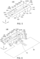
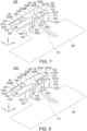
- the multiband antenna 10 may be formed by patterning a conductive layer (not shown) formed on a dielectric substrate (not shown). At any rate, the multiband antenna 10 is connected to a host conductor (80, see Figs. 6 to 8 ) when used. In detail, the first ground terminal 14 and the second ground terminal 16 are connected to the host conductor when the multiband antenna 10 is used.
- the host conductor may be a conductor layer formed on a substrate on which the multiband antenna 10 is mounted.
- the host conductor may be made of the conductive layer of which the multiband antenna 10 is made or may be made of another conductive layer, such as a ground plane, of the multilayer substrate.
- the host conductor may be a metal case of a communication device including the multiband antenna 10 or a metal plate for heat radiation.
- the multiband antenna 10 uses an external conductor as the host conductor (80, see Figs. 6 to 8 ), so that the antenna itself can be reduced in size. Moreover, by appropriately arranging the first ground terminal 14 and the second ground terminal 16, high radiation efficiency can be realized.
- the multiband antenna 10 according to the present embodiment may be modified as follows.
- the same or the similar components are represented by the same or the similar reference signs and the description thereof are omitted.
- a multiband antenna 10A according to a first modification is provided with a radiation element 20 in addition to the structure of the multiband antenna 10.
- the radiation element 20 has a first part 22 and a second part 24.
- the first part 22 of the radiation element 20 has a rectangular shape long in the second direction.
- the second part 24 of the radiation element 20 has a rectangular shape long in the first direction.
- the first part 22 of the radiation element 20 extends from the first long edge 125 of the conductor main portion 12 so as to go away from the slot 130.
- the second part 24 of the radiation element 20 extends from the first part 22 in a negative X-direction along the first direction.
- the first part 22 of the radiation element 20 has a first length L1 in the second direction
- the second part 24 of the radiation element 20 has a second length L2 in the first direction.
- the second length L2 is set to be longer than the first length L1.
- the first length L1 and the second length L2 are decided on the basis of a third resonance frequency that the radiation element 20 should have.
- the first part 22 of the radiation element 20 is nearer to the first slot 132 than to the second slot 134. Moreover, the first part 22, at least in part, is nearer to the opening portion 136 than to the middle M of the slot 130 in the first direction.
- the first part 22 has a first edge 221, a second edge 223 and a third edge 225.
- the third edge 225 of the first part 22 is located between the opening portion 136 and the middle M of the slot 130 in the first direction.
- a position of the first edge 221 of the first part 22 in the first direction is nearer to the middle M of the slot 130 than to the first short edge 121.
- the second part 24 of the radiation element 20 has a first edge 241, a second edge 243 and a third edge 245.
- a position of the first edge 241 of the second part 24 in the second direction coincides with a position of the second edge 223 of the first part 22.
- the second part 24 is away from the first long edge 125 of the conductor main portion 12.
- a size of the second part 24 is smaller than the first length L1 of the first part 22.
- a position of the second edge 243 of the second part 24 is between the second short edge 123 of the conductor main portion 12 and the opening portion 136.
- a multiband antenna 10B according to a second modification is provided with a radiation element 20B having a shape different from that of the radiation element 20 of the multiband antenna 10A.
- the radiation element 20B has a first part 22B and a second part 24.
- the first part 22B has a rectangular shape long in the first direction. In the first direction, a position of a first edge 221B of the first part 22B coincides with a position of the first short edge 121 of the conductor main portion 12.
- Each of the multiband antennas 10, 10A and 10B is formed two-dimensionally. However, the present invention is not limited thereto.
- the multiband antenna of the present invention may be formed three-dimensionally as in each of third to fifteenth modifications mentioned below.
- Each of the three-dimensional multiband antennas can be formed by punching and bending a single metal plate, for example.
- the present invention is not limited thereto.
- Each of the multiband antennas may be formed by combining a plurality of conductive plates. Moreover, if necessary, in order to improve strength, one or more conductive plates may be combined with a support, which is made of insulation resin, for example.
- a multiband antenna 10C according to the third modification has a conductor main portion 12, a first ground terminal 14C and second ground terminal 16C similarly to the multiband antenna 10 of Fig. 1 .
- each of the first ground terminal 14C and the second ground terminal 16C has a part extending from the second long edge 127 of the conductor main portion 12 in a direction intersecting with the conductor main portion 12 or with the horizontal plane.
- each of the first ground terminal 14C and the second ground terminal 16C extends downward along an up-down direction in whole.
- the up-down direction is a Z-direction.
- a positive Z-direction is directed upward while a negative Z-direction is directed downward.
- the multiband antenna 10C of Fig. 4 has the parts extending in the direction intersecting with the conductor main portion 12 or the horizontal plane, so that a distance from the conductor main portion 12 to the host conductor 80 can be increased without increasing an occupied area of the multiband antenna 10C when viewed along the up-down direction.
- the multiband antenna 10C can be hard to be influenced from the host conductor 80.
- a multiband antenna 10D according to the fourth modification is similar to the multiband antenna 10B according to the second modification. However, the multiband antenna 10D is provided with a first ground terminal 14C and a second ground terminal 16C which extend downward similarly to those of the multiband antenna 10C.
- the multiband antenna of the present invention may be further provided with a feeding terminal 30 or 30F as in each of fifth to seventh modifications.
- the feeding terminal 30 or 30F has a part intersecting with the horizontal plane, so that each of multiband antennas 10E to 10G can be surface-mounted on a circuit board (not shown) which is an object.
- the multiband antenna 10E according to the fifth modification is further provided with the feeding terminal 30 in addition to the structure of the multiband antenna 10D according to the fourth modification.
- the feeding terminal 30 has a rectangular shape and is provided to the conductor main portion 12.
- the conductor main portion 12 has a facing portion 1250 and a connection portion 1270 which are arranged to interpose the slot 130 therebetween, and the feeding terminal 30 is provided to the facing portion 1250.
- the feeding terminal 30 has a part extending from an inner edge of the first slot 132 defined by the facing portion 1250 in the direction intersecting with the horizontal plane. In the present modification, the feeding terminal 30 extends downward in whole.
- the facing portion 1250 is a part located between the first long edge 125 of the conductor main portion 12 and the slot 130
- the connection portion 1270 is a part located between the second long edge 127 of the conductor main portion 12 and the slot 130.
- the feeding terminal 30 is made of the same metal plate as the conductor main portion 12.
- the feeding terminal 30 is provided on a side of the first short edge 121 in the first direction when viewed from the opening portion 136.
- the first ground terminal 14C is located on the side of the first short edge 121 at least in part when viewed from the feeding terminal 30, and the second ground terminal 16C is located on the side of the second short edge 123 at least in part when viewed from the feeding terminal 30.
- the whole of the first ground terminal 14C is located on the side of the first short edge 121 when viewed from the feeding terminal 30, and the whole of the second ground terminal 16C is located on the side of the second short edge 123 when viewed from the feeding terminal 30.
- the feeding terminal 30 is connected to a feeding line 70 formed on an object (not shown) when mounted on the object. Moreover, both of the first ground terminal 14C and the second ground terminal 16C are connected to the host conductor 80.
- the object is a multilayer substrate, for example.
- the feeding line 70 and the host conductor 80 are formed of the same conductor layer included in the multilayer substrate or formed of different conductor layers included in the multilayer substrate.
- the multiband antenna 10F according to the sixth modification has the feeding terminal 30F having a shape different from that of the feeding terminal 30 of the multiband antenna 10E according to the fifth modification.
- the feeding terminal 30F has a first feeding portion 32 and a second feeding portion 34.
- the first feeding portion 32 extends from the facing portion 1250 of the conductor main portion 12 in the horizontal plane.
- the second feeding portion 34 extends, in the direction intersecting with the horizontal plane, from one end of the first feeding portion 32 in the first direction.
- the first feeding portion 32 extends from the inner edge of the first slot 132 in the negative Y-direction and protrudes in the first slot 132.
- the second feeding portion 34 extends downward from a negative X-side edge of the first feeding portion 32.
- the feeding terminal 30 of the multiband antenna 10E of Fig. 6 needs to be formed separately from the conductor main portion 12, and then to be connected to the conductor main portion 12.
- the feeding terminal 30F of the multiband antenna 10F according to the present modification can be formed by cutting and bending the same metal plate as the conductor main portion 12. Accordingly, the multiband antenna 10F is easy to be manufactured in comparison with the multiband antenna 10E.
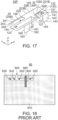
- the multiband antenna 10G according to the seventh modification is further provided with a stub 40 in addition to the structure of the multiband antenna 10F according to the sixth modification.
- the stub 40 is provided to the conductor main portion 12 to across the slot 130 approximately.
- the stub 40 is between the feeding terminal 30F and the first short edge 121 in the first direction.
- One end of the stub 40 is connected to the connection portion 1270, and the stub 40 extends toward the facing portion 1250.
- the stub 40 does not reach the facing portion 1250, and the other end of the stub 40 is apart from the facing portion 1250 and faces the facing portion 1250.
- the stub 40 is formed of the same metal plate as the conductor main portion 12 in conjunction with the feeding terminal 30F. Accordingly, the multiband antenna 10G is easy to be manufactured in comparison with the multiband antenna 10E.
- the present invention is not limited thereto.
- the stub 40 may be located between the feeding terminal 30F and the second short edge 123 in the first direction. The position of the stub 40 in the first direction is decided on the basis of a desired characteristic.
- the conductor main portion 12 is formed two-dimensionally.
- the present invention is not limited thereto.
- the conductor main portion 12 may be formed three-dimensionally as in each of eighth to twelfth modifications mentioned below.
- a multiband antenna 10H according to the eighth modification has an extension portion 50 in addition to the structure of the multiband antenna 10C according to the third modification.
- the extension portion 50 has a first extension portion 52 and a second extension portion 54.
- Each of the first extension portion 52 and the second extension portion 54 has a rectangular shape long in the first direction.
- the first extension portion 52 and the second extension portion 54 are arranged in the first direction to interpose the opening portion 136 therebetween.
- Both of the first extension portion 52 and the second extension portion 54 extend from the first long edge 125 of the conductor main portion 12 in the direction intersecting with the horizontal plane.
- the first extension portion 52 and the second extension portion 54 extend downward. Since the multiband antenna 10H has the extension portion 50, radiation efficiency thereof can be increased without increasing an occupied area thereof when viewed along the up-down direction.
- a multiband antenna 101 according to the ninth modification has an extension portion 501 different from that of the multiband antenna 10H according to the eighth modification.
- the extension portion 50I has a first extension portion 52I and a second extension portion 54I.
- the first extension portion 52I and the second extension portion 54I extend upward from the first long edge 125 of the conductor main portion 12.
- a multiband antenna 10J according to the tenth modification has an extension portion 50J different from that of the multiband antenna 10H according to the fifth modification.
- the extension portion 50J has a rectangular shape long in the second direction and extends from the second short edge 123 of the conductor main portion 12 in the direction intersecting with the horizontal plane. In the present modification, the extension portion 50J extends downward. However, the present invention is not limited thereto. The extension portion 50J may extend upward.
- a multiband antenna 10K according to the eleventh modification has an extension portion 50J in addition to the structure of the multiband antenna 10D according to the fourth modification.
- the extension portion 50J may extend upward.
- a multiband antenna 10L according to the twelfth modification further has an additional extension portion 60 in addition to the structure of the multiband antenna 10H according to the eighth modification.
- the additional extension portion 60 has a first additional extension portion 62 and a second additional extension portion 64.
- Each of the first additional extension portion 62 and the second additional extension portion 64 has a rectangular shape long in the first direction.
- the first additional extension portion 62 and the second additional extension portion 64 extend from a lower edge of the first extension portion 52 and a lower edge of the second extension portion 54, respectively, in the negative Y-direction along the second direction. Since the multiband antenna 10L has the additional extension portion 60, the radiation efficiency thereof can be increased without increasing an occupied area thereof when viewed along the up-down direction.
- the radiation element 20 is formed two-dimensionally.
- the present invention is not limited thereto.
- the radiation element 20 may be formed three-dimensionally as in each of thirteenth to fifteenth modifications mentioned below. If so, radiation efficiency of the multiband antenna can be increased without increasing an occupied area of the antenna when viewed along the up-down direction.
- a multiband antenna 10M according to the thirteenth modification has a radiation element 20M different, in shape, from the radiation element 20 of the multiband antenna 10D according to the fifth modification.
- the radiation element 20M is bent along the second direction and thereby has a first radiation portion 2010 and a second radiation portion 2020.
- the first radiation portion 2010 has the same shape as the radiation element 20 in the multiband antenna 10D.
- the second radiation portion 2020 extends from an edge of the first radiation portion 2010 in the direction intersecting with the horizontal plane. In the present modification, the second radiation portion 2020 extends downward.
- a multiband antenna 10N according to the fourteenth modification has a radiation element 20N different, in shape, from the radiation element 20M of the multiband antenna 10M according to the thirteenth modification.
- the radiation element 20N is bent along the second direction and thereby has a first radiation portion 2010 and a second radiation portion 2020N.
- the first radiation portion 2010 has the same shape as the radiation element 20 in the multiband antenna 10D.
- the second radiation portion 2020N extends upward from an edge of the first radiation portion 2010 in the second direction.
- a multiband antenna 10O according to the fifteen modification has a radiation element 20O different, in shape, from the radiation element 20M of the multiband antenna 10M according to the thirteenth modification.
- the radiation element 20O further has a third radiation portion 2030 in addition to the first radiation portion 2010 and the second radiation portion 2020.
- the third radiation portion 2030 extends from a lower edge of the second radiation portion 2020 in a direction intersecting with the second radiation portion 2020.
- the third radiation portion 2030 extends in the negative Y-direction along the second direction. Since the multiband antenna 10O has the third radiation portion 2030, radiation efficiency of the radiation element 20O can be further increased.
- the feeding terminal 30 or 30F is applicable to each of the multiband antennas 10C and 10H to 10O of the third and the eighth to the fifteenth modifications.
- the stub 40 is applicable to each of the multiband antennas 10C and 10H to 10O of the third and the eighth to the fifteenth modifications.
- a stub 40P may have an L-shape.
- the stub 40P extends from the connection portion 1270 in the positive Y-direction along the second direction and further extends in the positive X-direction along the first direction. In the second direction, one end of the stub 40P is connected to the connection portion 1270 while the other end of the stub 40P is apart from and faces the facing portion 1250. Since the stub 40P has the L-shape, an electric length of the stub 40P can be set without being limited by a size of the slot 130 in the second direction.
Landscapes
- Physics & Mathematics (AREA)
- Engineering & Computer Science (AREA)
- Remote Sensing (AREA)
- Fluid Mechanics (AREA)
- Astronomy & Astrophysics (AREA)
- Aviation & Aerospace Engineering (AREA)
- General Physics & Mathematics (AREA)
- Waveguide Aerials (AREA)
- Details Of Aerials (AREA)
Applications Claiming Priority (1)
| Application Number | Priority Date | Filing Date | Title |
|---|---|---|---|
| JP2021084565A JP7608267B2 (ja) | 2021-05-19 | 2021-05-19 | マルチバンドアンテナ |
Publications (2)
| Publication Number | Publication Date |
|---|---|
| EP4092827A1 EP4092827A1 (en) | 2022-11-23 |
| EP4092827B1 true EP4092827B1 (en) | 2024-08-07 |
Family
ID=81306967
Family Applications (1)
| Application Number | Title | Priority Date | Filing Date |
|---|---|---|---|
| EP22167249.6A Active EP4092827B1 (en) | 2021-05-19 | 2022-04-07 | Multiband antenna |
Country Status (6)
| Country | Link |
|---|---|
| US (1) | US20220376404A1 (https=) |
| EP (1) | EP4092827B1 (https=) |
| JP (1) | JP7608267B2 (https=) |
| KR (1) | KR102707259B1 (https=) |
| CN (1) | CN115395225B (https=) |
| TW (1) | TWI888718B (https=) |
Families Citing this family (2)
| Publication number | Priority date | Publication date | Assignee | Title |
|---|---|---|---|---|
| EP4429021A1 (en) * | 2023-03-09 | 2024-09-11 | Nokia Technologies Oy | An antenna arrangement |
| TWI911681B (zh) * | 2024-03-19 | 2026-01-11 | 啓碁科技股份有限公司 | 天線結構及電子裝置 |
Family Cites Families (26)
| Publication number | Priority date | Publication date | Assignee | Title |
|---|---|---|---|---|
| JPH10513329A (ja) * | 1995-02-06 | 1998-12-15 | メガウエイブ コーポレーション | 窓ガラスアンテナ |
| US6466170B2 (en) | 2001-03-28 | 2002-10-15 | Motorola, Inc. | Internal multi-band antennas for mobile communications |
| US6621455B2 (en) * | 2001-12-18 | 2003-09-16 | Nokia Corp. | Multiband antenna |
| DE60319965T2 (de) * | 2003-06-12 | 2009-04-30 | Research In Motion Ltd., Waterloo | Mehrelement-Antenne mit parasitärem Antennenelement |
| FI120606B (fi) * | 2003-10-20 | 2009-12-15 | Pulse Finland Oy | Sisäinen monikaista-antenni |
| KR100964652B1 (ko) * | 2007-05-03 | 2010-06-22 | 주식회사 이엠따블유 | 다중 대역 안테나 및 그를 포함하는 무선 통신 장치 |
| US8344962B2 (en) | 2008-11-20 | 2013-01-01 | Nokia Corporation | Apparatus, method and computer program for wireless communication |
| CN102326296A (zh) * | 2009-02-19 | 2012-01-18 | 盖尔创尼克斯有限公司 | 紧凑型多频带天线 |
| KR101714814B1 (ko) | 2009-09-22 | 2017-03-09 | 쓰리엠 이노베이티브 프로퍼티즈 컴파니 | 다공성 비세라믹 기판상에 원자층 증착 코팅을 도포하는 방법 |
| JP5699820B2 (ja) | 2010-09-16 | 2015-04-15 | 日本電気株式会社 | アンテナ装置 |
| WO2013124897A1 (ja) * | 2012-02-23 | 2013-08-29 | 日本電気株式会社 | アンテナ装置 |
| KR101321195B1 (ko) * | 2012-03-26 | 2013-10-23 | 아우덴 테크노 코포레이션 | 다중-대역 안테나 구조체 |
| US10476132B2 (en) * | 2014-03-31 | 2019-11-12 | Nec Corporation | Antenna, antenna array, and radio communication apparatus |
| TWI543445B (zh) * | 2014-08-12 | 2016-07-21 | 智易科技股份有限公司 | 天線及其製造方法 |
| US20170301997A1 (en) * | 2014-09-26 | 2017-10-19 | Nec Corporation | Antenna array, wireless communication apparatus, and method for making antenna array |
| JP2018074263A (ja) * | 2016-10-25 | 2018-05-10 | 旭硝子株式会社 | 車両用アンテナ及びアンテナ付き窓ガラス |
| JP6659519B2 (ja) * | 2016-11-02 | 2020-03-04 | 株式会社東芝 | アンテナ装置 |
| EP3583659A1 (en) * | 2017-02-20 | 2019-12-25 | Smart Antenna Technologies Ltd | Triple wideband hybrid lte slot antenna |
| EP3474376B1 (en) * | 2017-10-17 | 2022-07-27 | Advanced Automotive Antennas, S.L.U. | Broadband antenna system |
| JP6341399B1 (ja) | 2018-03-14 | 2018-06-13 | パナソニックIpマネジメント株式会社 | アンテナ装置 |
| WO2019198588A1 (ja) * | 2018-04-12 | 2019-10-17 | 日本電気株式会社 | スプリットリング共振器、基板、及びコネクタ |
| EP3582323B1 (en) * | 2018-06-15 | 2021-12-29 | Advanced Automotive Antennas, S.L.U. | Dual broadband antenna system for vehicles |
| WO2020144994A1 (ja) * | 2019-01-10 | 2020-07-16 | 日本電気株式会社 | アンテナ及び通信装置 |
| JP7216576B2 (ja) * | 2019-03-05 | 2023-02-01 | 日本航空電子工業株式会社 | アンテナ |
| KR102542096B1 (ko) * | 2019-04-17 | 2023-06-13 | 니혼 고꾸 덴시 고교 가부시끼가이샤 | 스플릿 링 공진기 및 통신 장치 |
| CN115101924B (zh) | 2019-10-31 | 2026-03-13 | 华为终端有限公司 | 天线装置及电子设备 |
-
2021
- 2021-05-19 JP JP2021084565A patent/JP7608267B2/ja active Active
-
2022
- 2022-04-05 US US17/713,492 patent/US20220376404A1/en not_active Abandoned
- 2022-04-07 EP EP22167249.6A patent/EP4092827B1/en active Active
- 2022-04-11 TW TW111113625A patent/TWI888718B/zh active
- 2022-04-13 CN CN202210384251.9A patent/CN115395225B/zh active Active
- 2022-04-13 KR KR1020220045725A patent/KR102707259B1/ko active Active
Also Published As
| Publication number | Publication date |
|---|---|
| JP2022178055A (ja) | 2022-12-02 |
| CN115395225B (zh) | 2026-03-20 |
| EP4092827A1 (en) | 2022-11-23 |
| KR20220156746A (ko) | 2022-11-28 |
| US20220376404A1 (en) | 2022-11-24 |
| TW202249348A (zh) | 2022-12-16 |
| KR102707259B1 (ko) | 2024-09-13 |
| TWI888718B (zh) | 2025-07-01 |
| CN115395225A (zh) | 2022-11-25 |
| JP7608267B2 (ja) | 2025-01-06 |
Similar Documents
| Publication | Publication Date | Title |
|---|---|---|
| US7564413B2 (en) | Multi-band antenna and mobile communication terminal having the same | |
| EP2493011B1 (en) | Mobile communication device | |
| US8098203B2 (en) | Antenna and communication device having the same | |
| US9397405B2 (en) | Antenna device | |
| CN1886863A (zh) | 内部多频带天线 | |
| JP5093230B2 (ja) | アンテナおよび無線通信機 | |
| CN1972008A (zh) | 多频段天线部件 | |
| JP2001284954A (ja) | 表面実装型アンテナおよびその複共振の周波数調整設定方法および表面実装型アンテナを備えた通信装置 | |
| EP4200938B1 (en) | Miniature antenna with omnidirectional radiation field | |
| EP4092827B1 (en) | Multiband antenna | |
| EP1085595B1 (en) | Surface-mounted antenna and communication apparatus using same | |
| EP3244482B1 (en) | Dual band printed antenna | |
| JPWO2004097980A1 (ja) | 広帯域平板状アンテナ | |
| US8319691B2 (en) | Multi-band antenna | |
| JP6478510B2 (ja) | アンテナ | |
| EP2775566B1 (en) | Wireless terminal | |
| JP6865072B2 (ja) | アンテナ装置及びアンテナ装置を備えた電子機器 | |
| CN115249887B (zh) | 天线模块 | |
| KR100688648B1 (ko) | 단락 스터브를 이용한 이동통신단말기용 다중대역 내장형안테나 | |
| EP4266499B1 (en) | Multiband antenna | |
| US20110254737A1 (en) | Slotted antenna device | |
| CN215451754U (zh) | 天线和电子设备 | |
| HK40092442A (en) | Miniature antenna with omnidirectional radiation field | |
| HK40092442B (en) | Miniature antenna with omnidirectional radiation field | |
| KR20070098019A (ko) | 광대역 안테나 및 이를 구비한 전자기기 |
Legal Events
| Date | Code | Title | Description |
|---|---|---|---|
| PUAI | Public reference made under article 153(3) epc to a published international application that has entered the european phase |
Free format text: ORIGINAL CODE: 0009012 |
|
| STAA | Information on the status of an ep patent application or granted ep patent |
Free format text: STATUS: THE APPLICATION HAS BEEN PUBLISHED |
|
| AK | Designated contracting states |
Kind code of ref document: A1 Designated state(s): AL AT BE BG CH CY CZ DE DK EE ES FI FR GB GR HR HU IE IS IT LI LT LU LV MC MK MT NL NO PL PT RO RS SE SI SK SM TR |
|
| STAA | Information on the status of an ep patent application or granted ep patent |
Free format text: STATUS: REQUEST FOR EXAMINATION WAS MADE |
|
| 17P | Request for examination filed |
Effective date: 20230509 |
|
| RBV | Designated contracting states (corrected) |
Designated state(s): AL AT BE BG CH CY CZ DE DK EE ES FI FR GB GR HR HU IE IS IT LI LT LU LV MC MK MT NL NO PL PT RO RS SE SI SK SM TR |
|
| STAA | Information on the status of an ep patent application or granted ep patent |
Free format text: STATUS: EXAMINATION IS IN PROGRESS |
|
| 17Q | First examination report despatched |
Effective date: 20230804 |
|
| GRAP | Despatch of communication of intention to grant a patent |
Free format text: ORIGINAL CODE: EPIDOSNIGR1 |
|
| STAA | Information on the status of an ep patent application or granted ep patent |
Free format text: STATUS: GRANT OF PATENT IS INTENDED |
|
| INTG | Intention to grant announced |
Effective date: 20240227 |
|
| GRAS | Grant fee paid |
Free format text: ORIGINAL CODE: EPIDOSNIGR3 |
|
| GRAA | (expected) grant |
Free format text: ORIGINAL CODE: 0009210 |
|
| STAA | Information on the status of an ep patent application or granted ep patent |
Free format text: STATUS: THE PATENT HAS BEEN GRANTED |
|
| AK | Designated contracting states |
Kind code of ref document: B1 Designated state(s): AL AT BE BG CH CY CZ DE DK EE ES FI FR GB GR HR HU IE IS IT LI LT LU LV MC MK MT NL NO PL PT RO RS SE SI SK SM TR |
|
| REG | Reference to a national code |
Ref country code: GB Ref legal event code: FG4D |
|
| REG | Reference to a national code |
Ref country code: CH Ref legal event code: EP |
|
| REG | Reference to a national code |
Ref country code: IE Ref legal event code: FG4D |
|
| REG | Reference to a national code |
Ref country code: DE Ref legal event code: R096 Ref document number: 602022005069 Country of ref document: DE |
|
| REG | Reference to a national code |
Ref country code: LT Ref legal event code: MG9D |
|
| REG | Reference to a national code |
Ref country code: NL Ref legal event code: MP Effective date: 20240807 |
|
| PG25 | Lapsed in a contracting state [announced via postgrant information from national office to epo] |
Ref country code: NO Free format text: LAPSE BECAUSE OF FAILURE TO SUBMIT A TRANSLATION OF THE DESCRIPTION OR TO PAY THE FEE WITHIN THE PRESCRIBED TIME-LIMIT Effective date: 20241107 |
|
| REG | Reference to a national code |
Ref country code: AT Ref legal event code: MK05 Ref document number: 1711983 Country of ref document: AT Kind code of ref document: T Effective date: 20240807 |
|
| PG25 | Lapsed in a contracting state [announced via postgrant information from national office to epo] |
Ref country code: FI Free format text: LAPSE BECAUSE OF FAILURE TO SUBMIT A TRANSLATION OF THE DESCRIPTION OR TO PAY THE FEE WITHIN THE PRESCRIBED TIME-LIMIT Effective date: 20240807 Ref country code: PT Free format text: LAPSE BECAUSE OF FAILURE TO SUBMIT A TRANSLATION OF THE DESCRIPTION OR TO PAY THE FEE WITHIN THE PRESCRIBED TIME-LIMIT Effective date: 20241209 Ref country code: NL Free format text: LAPSE BECAUSE OF FAILURE TO SUBMIT A TRANSLATION OF THE DESCRIPTION OR TO PAY THE FEE WITHIN THE PRESCRIBED TIME-LIMIT Effective date: 20240807 Ref country code: PL Free format text: LAPSE BECAUSE OF FAILURE TO SUBMIT A TRANSLATION OF THE DESCRIPTION OR TO PAY THE FEE WITHIN THE PRESCRIBED TIME-LIMIT Effective date: 20240807 Ref country code: GR Free format text: LAPSE BECAUSE OF FAILURE TO SUBMIT A TRANSLATION OF THE DESCRIPTION OR TO PAY THE FEE WITHIN THE PRESCRIBED TIME-LIMIT Effective date: 20241108 |
|
| PG25 | Lapsed in a contracting state [announced via postgrant information from national office to epo] |
Ref country code: BG Free format text: LAPSE BECAUSE OF FAILURE TO SUBMIT A TRANSLATION OF THE DESCRIPTION OR TO PAY THE FEE WITHIN THE PRESCRIBED TIME-LIMIT Effective date: 20240807 |
|
| PG25 | Lapsed in a contracting state [announced via postgrant information from national office to epo] |
Ref country code: LV Free format text: LAPSE BECAUSE OF FAILURE TO SUBMIT A TRANSLATION OF THE DESCRIPTION OR TO PAY THE FEE WITHIN THE PRESCRIBED TIME-LIMIT Effective date: 20240807 |
|
| PG25 | Lapsed in a contracting state [announced via postgrant information from national office to epo] |
Ref country code: AT Free format text: LAPSE BECAUSE OF FAILURE TO SUBMIT A TRANSLATION OF THE DESCRIPTION OR TO PAY THE FEE WITHIN THE PRESCRIBED TIME-LIMIT Effective date: 20240807 Ref country code: IS Free format text: LAPSE BECAUSE OF FAILURE TO SUBMIT A TRANSLATION OF THE DESCRIPTION OR TO PAY THE FEE WITHIN THE PRESCRIBED TIME-LIMIT Effective date: 20241207 |
|
| PG25 | Lapsed in a contracting state [announced via postgrant information from national office to epo] |
Ref country code: HR Free format text: LAPSE BECAUSE OF FAILURE TO SUBMIT A TRANSLATION OF THE DESCRIPTION OR TO PAY THE FEE WITHIN THE PRESCRIBED TIME-LIMIT Effective date: 20240807 |
|
| PG25 | Lapsed in a contracting state [announced via postgrant information from national office to epo] |
Ref country code: RS Free format text: LAPSE BECAUSE OF FAILURE TO SUBMIT A TRANSLATION OF THE DESCRIPTION OR TO PAY THE FEE WITHIN THE PRESCRIBED TIME-LIMIT Effective date: 20241107 Ref country code: ES Free format text: LAPSE BECAUSE OF FAILURE TO SUBMIT A TRANSLATION OF THE DESCRIPTION OR TO PAY THE FEE WITHIN THE PRESCRIBED TIME-LIMIT Effective date: 20240807 |
|
| PG25 | Lapsed in a contracting state [announced via postgrant information from national office to epo] |
Ref country code: RS Free format text: LAPSE BECAUSE OF FAILURE TO SUBMIT A TRANSLATION OF THE DESCRIPTION OR TO PAY THE FEE WITHIN THE PRESCRIBED TIME-LIMIT Effective date: 20241107 Ref country code: PT Free format text: LAPSE BECAUSE OF FAILURE TO SUBMIT A TRANSLATION OF THE DESCRIPTION OR TO PAY THE FEE WITHIN THE PRESCRIBED TIME-LIMIT Effective date: 20241209 Ref country code: PL Free format text: LAPSE BECAUSE OF FAILURE TO SUBMIT A TRANSLATION OF THE DESCRIPTION OR TO PAY THE FEE WITHIN THE PRESCRIBED TIME-LIMIT Effective date: 20240807 Ref country code: NO Free format text: LAPSE BECAUSE OF FAILURE TO SUBMIT A TRANSLATION OF THE DESCRIPTION OR TO PAY THE FEE WITHIN THE PRESCRIBED TIME-LIMIT Effective date: 20241107 Ref country code: NL Free format text: LAPSE BECAUSE OF FAILURE TO SUBMIT A TRANSLATION OF THE DESCRIPTION OR TO PAY THE FEE WITHIN THE PRESCRIBED TIME-LIMIT Effective date: 20240807 Ref country code: LV Free format text: LAPSE BECAUSE OF FAILURE TO SUBMIT A TRANSLATION OF THE DESCRIPTION OR TO PAY THE FEE WITHIN THE PRESCRIBED TIME-LIMIT Effective date: 20240807 Ref country code: IS Free format text: LAPSE BECAUSE OF FAILURE TO SUBMIT A TRANSLATION OF THE DESCRIPTION OR TO PAY THE FEE WITHIN THE PRESCRIBED TIME-LIMIT Effective date: 20241207 Ref country code: HR Free format text: LAPSE BECAUSE OF FAILURE TO SUBMIT A TRANSLATION OF THE DESCRIPTION OR TO PAY THE FEE WITHIN THE PRESCRIBED TIME-LIMIT Effective date: 20240807 Ref country code: GR Free format text: LAPSE BECAUSE OF FAILURE TO SUBMIT A TRANSLATION OF THE DESCRIPTION OR TO PAY THE FEE WITHIN THE PRESCRIBED TIME-LIMIT Effective date: 20241108 Ref country code: FI Free format text: LAPSE BECAUSE OF FAILURE TO SUBMIT A TRANSLATION OF THE DESCRIPTION OR TO PAY THE FEE WITHIN THE PRESCRIBED TIME-LIMIT Effective date: 20240807 Ref country code: ES Free format text: LAPSE BECAUSE OF FAILURE TO SUBMIT A TRANSLATION OF THE DESCRIPTION OR TO PAY THE FEE WITHIN THE PRESCRIBED TIME-LIMIT Effective date: 20240807 Ref country code: BG Free format text: LAPSE BECAUSE OF FAILURE TO SUBMIT A TRANSLATION OF THE DESCRIPTION OR TO PAY THE FEE WITHIN THE PRESCRIBED TIME-LIMIT Effective date: 20240807 Ref country code: AT Free format text: LAPSE BECAUSE OF FAILURE TO SUBMIT A TRANSLATION OF THE DESCRIPTION OR TO PAY THE FEE WITHIN THE PRESCRIBED TIME-LIMIT Effective date: 20240807 |
|
| PG25 | Lapsed in a contracting state [announced via postgrant information from national office to epo] |
Ref country code: DK Free format text: LAPSE BECAUSE OF FAILURE TO SUBMIT A TRANSLATION OF THE DESCRIPTION OR TO PAY THE FEE WITHIN THE PRESCRIBED TIME-LIMIT Effective date: 20240807 Ref country code: SM Free format text: LAPSE BECAUSE OF FAILURE TO SUBMIT A TRANSLATION OF THE DESCRIPTION OR TO PAY THE FEE WITHIN THE PRESCRIBED TIME-LIMIT Effective date: 20240807 |
|
| PG25 | Lapsed in a contracting state [announced via postgrant information from national office to epo] |
Ref country code: EE Free format text: LAPSE BECAUSE OF FAILURE TO SUBMIT A TRANSLATION OF THE DESCRIPTION OR TO PAY THE FEE WITHIN THE PRESCRIBED TIME-LIMIT Effective date: 20240807 |
|
| PG25 | Lapsed in a contracting state [announced via postgrant information from national office to epo] |
Ref country code: CZ Free format text: LAPSE BECAUSE OF FAILURE TO SUBMIT A TRANSLATION OF THE DESCRIPTION OR TO PAY THE FEE WITHIN THE PRESCRIBED TIME-LIMIT Effective date: 20240807 |
|
| PG25 | Lapsed in a contracting state [announced via postgrant information from national office to epo] |
Ref country code: SK Free format text: LAPSE BECAUSE OF FAILURE TO SUBMIT A TRANSLATION OF THE DESCRIPTION OR TO PAY THE FEE WITHIN THE PRESCRIBED TIME-LIMIT Effective date: 20240807 |
|
| REG | Reference to a national code |
Ref country code: DE Ref legal event code: R097 Ref document number: 602022005069 Country of ref document: DE |
|
| PLBE | No opposition filed within time limit |
Free format text: ORIGINAL CODE: 0009261 |
|
| STAA | Information on the status of an ep patent application or granted ep patent |
Free format text: STATUS: NO OPPOSITION FILED WITHIN TIME LIMIT |
|
| PGFP | Annual fee paid to national office [announced via postgrant information from national office to epo] |
Ref country code: DE Payment date: 20250429 Year of fee payment: 4 |
|
| 26N | No opposition filed |
Effective date: 20250508 |
|
| PG25 | Lapsed in a contracting state [announced via postgrant information from national office to epo] |
Ref country code: SE Free format text: LAPSE BECAUSE OF FAILURE TO SUBMIT A TRANSLATION OF THE DESCRIPTION OR TO PAY THE FEE WITHIN THE PRESCRIBED TIME-LIMIT Effective date: 20240807 |
|
| REG | Reference to a national code |
Ref country code: CH Ref legal event code: H13 Free format text: ST27 STATUS EVENT CODE: U-0-0-H10-H13 (AS PROVIDED BY THE NATIONAL OFFICE) Effective date: 20251125 |
|
| PG25 | Lapsed in a contracting state [announced via postgrant information from national office to epo] |
Ref country code: LU Free format text: LAPSE BECAUSE OF NON-PAYMENT OF DUE FEES Effective date: 20250407 |
|
| PG25 | Lapsed in a contracting state [announced via postgrant information from national office to epo] |
Ref country code: MC Free format text: LAPSE BECAUSE OF FAILURE TO SUBMIT A TRANSLATION OF THE DESCRIPTION OR TO PAY THE FEE WITHIN THE PRESCRIBED TIME-LIMIT Effective date: 20240807 |
|
| REG | Reference to a national code |
Ref country code: BE Ref legal event code: MM Effective date: 20250430 |
|
| PG25 | Lapsed in a contracting state [announced via postgrant information from national office to epo] |
Ref country code: BE Free format text: LAPSE BECAUSE OF NON-PAYMENT OF DUE FEES Effective date: 20250430 |
|
| PG25 | Lapsed in a contracting state [announced via postgrant information from national office to epo] |
Ref country code: CH Free format text: LAPSE BECAUSE OF NON-PAYMENT OF DUE FEES Effective date: 20250430 |
|
| PG25 | Lapsed in a contracting state [announced via postgrant information from national office to epo] |
Ref country code: IT Free format text: LAPSE BECAUSE OF FAILURE TO SUBMIT A TRANSLATION OF THE DESCRIPTION OR TO PAY THE FEE WITHIN THE PRESCRIBED TIME-LIMIT Effective date: 20240807 |
|
| PGFP | Annual fee paid to national office [announced via postgrant information from national office to epo] |
Ref country code: GB Payment date: 20260313 Year of fee payment: 5 |
|
| PG25 | Lapsed in a contracting state [announced via postgrant information from national office to epo] |
Ref country code: IE Free format text: LAPSE BECAUSE OF NON-PAYMENT OF DUE FEES Effective date: 20250407 |
|
| PG25 | Lapsed in a contracting state [announced via postgrant information from national office to epo] |
Ref country code: RO Free format text: LAPSE BECAUSE OF FAILURE TO SUBMIT A TRANSLATION OF THE DESCRIPTION OR TO PAY THE FEE WITHIN THE PRESCRIBED TIME-LIMIT Effective date: 20240807 |
|
| PGFP | Annual fee paid to national office [announced via postgrant information from national office to epo] |
Ref country code: FR Payment date: 20260309 Year of fee payment: 5 |