EP4092747B1 - Anzeigevorrichtung mit lichtemittierendem halbleiterbauelement - Google Patents
Anzeigevorrichtung mit lichtemittierendem halbleiterbauelement Download PDFInfo
- Publication number
- EP4092747B1 EP4092747B1 EP20914448.4A EP20914448A EP4092747B1 EP 4092747 B1 EP4092747 B1 EP 4092747B1 EP 20914448 A EP20914448 A EP 20914448A EP 4092747 B1 EP4092747 B1 EP 4092747B1
- Authority
- EP
- European Patent Office
- Prior art keywords
- light emitting
- semiconductor light
- emitting diode
- conductivity type
- layer
- Prior art date
- Legal status (The legal status is an assumption and is not a legal conclusion. Google has not performed a legal analysis and makes no representation as to the accuracy of the status listed.)
- Active
Links
Images


Classifications
-
- H—ELECTRICITY
- H10—SEMICONDUCTOR DEVICES; ELECTRIC SOLID-STATE DEVICES NOT OTHERWISE PROVIDED FOR
- H10H—INORGANIC LIGHT-EMITTING SEMICONDUCTOR DEVICES HAVING POTENTIAL BARRIERS
- H10H29/00—Integrated devices, or assemblies of multiple devices, comprising at least one light-emitting semiconductor element covered by group H10H20/00
- H10H29/10—Integrated devices comprising at least one light-emitting semiconductor component covered by group H10H20/00
- H10H29/14—Integrated devices comprising at least one light-emitting semiconductor component covered by group H10H20/00 comprising multiple light-emitting semiconductor components
- H10H29/142—Two-dimensional arrangements, e.g. asymmetric LED layout
-
- H—ELECTRICITY
- H10—SEMICONDUCTOR DEVICES; ELECTRIC SOLID-STATE DEVICES NOT OTHERWISE PROVIDED FOR
- H10H—INORGANIC LIGHT-EMITTING SEMICONDUCTOR DEVICES HAVING POTENTIAL BARRIERS
- H10H20/00—Individual inorganic light-emitting semiconductor devices having potential barriers, e.g. light-emitting diodes [LED]
- H10H20/80—Constructional details
- H10H20/81—Bodies
- H10H20/819—Bodies characterised by their shape, e.g. curved or truncated substrates
- H10H20/82—Roughened surfaces, e.g. at the interface between epitaxial layers
-
- H—ELECTRICITY
- H10—SEMICONDUCTOR DEVICES; ELECTRIC SOLID-STATE DEVICES NOT OTHERWISE PROVIDED FOR
- H10H—INORGANIC LIGHT-EMITTING SEMICONDUCTOR DEVICES HAVING POTENTIAL BARRIERS
- H10H20/00—Individual inorganic light-emitting semiconductor devices having potential barriers, e.g. light-emitting diodes [LED]
- H10H20/80—Constructional details
- H10H20/81—Bodies
- H10H20/822—Materials of the light-emitting regions
- H10H20/824—Materials of the light-emitting regions comprising only Group III-V materials, e.g. GaP
- H10H20/825—Materials of the light-emitting regions comprising only Group III-V materials, e.g. GaP containing nitrogen, e.g. GaN
-
- H—ELECTRICITY
- H10—SEMICONDUCTOR DEVICES; ELECTRIC SOLID-STATE DEVICES NOT OTHERWISE PROVIDED FOR
- H10H—INORGANIC LIGHT-EMITTING SEMICONDUCTOR DEVICES HAVING POTENTIAL BARRIERS
- H10H20/00—Individual inorganic light-emitting semiconductor devices having potential barriers, e.g. light-emitting diodes [LED]
- H10H20/80—Constructional details
- H10H20/83—Electrodes
- H10H20/831—Electrodes characterised by their shape
-
- H—ELECTRICITY
- H10—SEMICONDUCTOR DEVICES; ELECTRIC SOLID-STATE DEVICES NOT OTHERWISE PROVIDED FOR
- H10H—INORGANIC LIGHT-EMITTING SEMICONDUCTOR DEVICES HAVING POTENTIAL BARRIERS
- H10H20/00—Individual inorganic light-emitting semiconductor devices having potential barriers, e.g. light-emitting diodes [LED]
- H10H20/80—Constructional details
- H10H20/85—Packages
- H10H20/8506—Containers
-
- H—ELECTRICITY
- H10—SEMICONDUCTOR DEVICES; ELECTRIC SOLID-STATE DEVICES NOT OTHERWISE PROVIDED FOR
- H10H—INORGANIC LIGHT-EMITTING SEMICONDUCTOR DEVICES HAVING POTENTIAL BARRIERS
- H10H20/00—Individual inorganic light-emitting semiconductor devices having potential barriers, e.g. light-emitting diodes [LED]
- H10H20/80—Constructional details
- H10H20/85—Packages
- H10H20/857—Interconnections, e.g. lead-frames, bond wires or solder balls
-
- H—ELECTRICITY
- H10—SEMICONDUCTOR DEVICES; ELECTRIC SOLID-STATE DEVICES NOT OTHERWISE PROVIDED FOR
- H10W—GENERIC PACKAGES, INTERCONNECTIONS, CONNECTORS OR OTHER CONSTRUCTIONAL DETAILS OF DEVICES COVERED BY CLASS H10
- H10W90/00—Package configurations
-
- H—ELECTRICITY
- H10—SEMICONDUCTOR DEVICES; ELECTRIC SOLID-STATE DEVICES NOT OTHERWISE PROVIDED FOR
- H10H—INORGANIC LIGHT-EMITTING SEMICONDUCTOR DEVICES HAVING POTENTIAL BARRIERS
- H10H20/00—Individual inorganic light-emitting semiconductor devices having potential barriers, e.g. light-emitting diodes [LED]
- H10H20/01—Manufacture or treatment
-
- H—ELECTRICITY
- H10—SEMICONDUCTOR DEVICES; ELECTRIC SOLID-STATE DEVICES NOT OTHERWISE PROVIDED FOR
- H10W—GENERIC PACKAGES, INTERCONNECTIONS, CONNECTORS OR OTHER CONSTRUCTIONAL DETAILS OF DEVICES COVERED BY CLASS H10
- H10W72/00—Interconnections or connectors in packages
- H10W72/01—Manufacture or treatment
- H10W72/0198—Manufacture or treatment batch processes
Definitions
- the present invention relates to a display device using a semiconductor light emitting diode, and in particular, to a display device using a semiconductor light emitting diode having a size of several to several tens of ⁇ m.
- LCD liquid crystal displays
- OLED organic light-emitting diode
- micro LED displays are competing to implement a large-area display in the field of display technology.
- the display does not absorb light using a polarizing plate or the like, and thus, very high efficiency can be provided.
- a semiconductor light emitting diode microwave LED
- the display does not absorb light using a polarizing plate or the like, and thus, very high efficiency can be provided.
- a large display requires millions of semiconductor light emitting diodes, it is difficult to transfer the elements, compared to other technologies.
- the self-assembly is a method in which a semiconductor light emitting diode finds its own position in a fluid, and is the most advantageous method for realizing a large-screen display device.
- the self-assembly includes a method of directly assembling a semiconductor light emitting diode on a final substrate to be used in a product, and a method of assembling a semiconductor light emitting diode on an assembly substrate and then transferring the semiconductor light emitting diode to a final substrate through an additional transfer process.
- the method of directly assembling on the final substrate is efficient in terms of process.
- the use of the assembly substrate has an advantage in that a structure for self-assembly can be added without limitation. Therefore, the two methods are selectively used.
- One object of the present invention is to provide a display device having a structure (position selectivity) capable of self-assembling semiconductor light emitting diodes emitting different colors to a substrate at the same time.
- the semiconductor light emitting diode and the substrate each include a recessed portion and a solder portion corresponding thereto.
- Another object of the present invention is to provide a display device having a structure in which a semiconductor light emitting diode can be electrically connected to a substrate while being assembled to the substrate.
- a recessed portion and a solder portion may include an ohmic electrode and a wiring electrode for electrical connection.
- Another object of the present invention is to provide a display device having a structure capable of preventing separation of a semiconductor light emitting diode assembled on a substrate.
- a solder portion of the substrate may include a magnetic layer.
- the invention provides a display device according to the independent claim. Preferred embodiments are defined by the dependent claims.
- the display device can perform self-assembly by simultaneously inputting semiconductor light emitting diodes emitting different colors into a fluid chamber, thereby shortening the assembly time.
- the semiconductor light emitting diode seated in the cell can be connected to the wiring electrode through bonding with the solder portion, and furthermore, there is an effect that it can be more stably fixed to the substrate by the magnetic force acting between the semiconductor light emitting diode and the solder portion.
- the display device described herein may include mobile phones, smart phones, laptop computers, digital broadcasting terminals, personal digital assistants (PDA), portable multimedia players (PMP), navigation systems, slate PCs, a Tablet PC, Ultra Books, digital TVs, digital signages, head mounted displays (HMDs), desktop computers, and the like.
- PDA personal digital assistants
- PMP portable multimedia players
- slate PCs slate PCs
- Tablet PC Ultra Books
- digital TVs digital signages
- HDMDs head mounted displays
- desktop computers and the like.
- FIG. 1 is a conceptual diagram showing an embodiment of a display device using a semiconductor light emitting diode of the present invention
- FIG. 2 is a partially enlarged view of portion A of the display device of FIG. 1
- FIG. 3 is an enlarged view of the semiconductor light emitting diode of FIG. 2
- FIG. 4 is an enlarged view showing another embodiment of the semiconductor light emitting diode of FIG. 2 .
- information processed by a controller of a display device 100 may be output from a display module 140.
- a closed-loop-type case 101 surrounding edges of the display module may form a bezel of the display device.
- the display module 140 may include a panel 141 on which images are displayed, and the panel 141 may include a micro-sized semiconductor light emitting diode 150 and a wiring board 110 on which the semiconductor light emitting diode 150 is mounted.
- Wirings may be formed on the wiring board 110 to be connected to an n-type electrode 152 and a p-type electrode 156 of the semiconductor light emitting diode 150.
- the semiconductor light emitting diode 150 may be provided on the wiring board 110 as an individual pixel that emits light itself.
- An image displayed on the panel 141 is visual information, and is implemented by independently controlling light emission of sub-pixels arranged in a matrix form through the wirings.
- a micro LED Light Emitting Diode
- the micro LED may be a light emitting diode formed in a small size of 100 micro or less.
- blue, red, and green colors are provided in light emitting regions, respectively, and a unit pixel may be realized by a combination thereof. That is, the unit pixel may mean a minimum unit for realizing one color, and at least three micro LEDs may be provided in the unit pixel.
- the semiconductor light emitting diode 150 may have a vertical structure.
- the semiconductor light emitting diode 150 is mainly made of gallium nitride (GaN), and indium (In) and/or aluminum (Al) are added together to implement a high output light emitting diode that emits various lights including blue.
- GaN gallium nitride
- Al aluminum
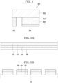
- the vertical semiconductor light emitting diode may include a p-type electrode 156, a p-type semiconductor layer 155 formed on the p-type electrode 156, an active layer 154 formed on the p-type semiconductor layer 155, an n-type semiconductor layer 153 formed on the active layer 154, and an n-type electrode 152 formed on the n-type semiconductor layer 153.
- the p-type electrode 156 positioned in a lower portion may be electrically connected to the p-electrode of the wiring board
- the n-type electrode 152 positioned in an upper portion may be electrically connected to the n-electrode at the upper side of the semiconductor light emitting diode.
- the vertical semiconductor light emitting diode 150 has a great advantage in that it is possible to reduce the chip size because electrodes are arranged up and down.
- the semiconductor light emitting diode may be a flip chip type light emitting diode.
- the semiconductor light emitting diode 250 may include a p-type electrode 256, a p-type semiconductor layer 255 on which the p-type electrode 256 is formed, an active layer 254 formed on the p-type semiconductor layer 255, an n-type semiconductor layer 253 formed on the active layer 254, and an n-type electrode 252 spaced apart from the p-type electrode 256 in the horizontal direction on the n-type semiconductor layer 253.
- both the p-type electrode 256 and the n-type electrode 152 may be electrically connected to the p-electrode and n-electrode of the wiring board under the semiconductor light emitting diode.
- the vertical semiconductor light emitting diode and the horizontal semiconductor light emitting diode may be a green semiconductor light emitting diode, a blue semiconductor light emitting diode, or a red semiconductor light emitting diode, respectively.
- gallium nitride (GaN) is mainly used, and indium (In) and/or aluminum (Al) are added together to implement a high output light emitting diode that emits green or blue light.
- the semiconductor light emitting diode may be a gallium nitride thin film formed in various layers such as n-Gan, p-Gan, AlGaN, InGan, etc.
- the p-type semiconductor layer may be P-type GaN, and the n-type semiconductor layer may be N-type GaN.
- the p-type semiconductor layer may be P-type GaAs, and the n-type semiconductor layer may be N-type GaAs.
- the p-type semiconductor layer may be P-type GaN doped with Mg on the p-electrode side
- the n-type semiconductor layer may be N-type GaN doped with Si on the n-electrode side.
- the above-described semiconductor light emitting diodes may be semiconductor light emitting diodes having no active layer.
- the light emitting diodes are very small, unit pixels that emit light themselves may be arranged in a high definition in the display panel, thereby realizing a high-definition display device.
- the semiconductor light emitting diode grown on a wafer and formed through mesa and isolation is used as an individual pixel.
- the micro-sized semiconductor light emitting diode 150 needs to be transferred to the wafer at a predetermined position on a substrate of the display panel.
- There is a pick and place technique as such a transfer technique but the success rate is low and a lot of time is required.
- there is a technique of transferring several devices at a time using a stamp or a roll but it is not suitable for a large screen display due to a limitation in yield.
- the present invention proposes a new manufacturing method and manufacturing apparatus for a display device that can solve these problems.
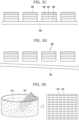
- FIGS. 5A to 5E are conceptual views for describing a new process of manufacturing the semiconductor light emitting diode.
- a display device using a passive matrix (PM) type semiconductor light emitting diode is taken as an example.
- PM passive matrix
- AM active matrix
- a method of self-assembling a horizontal semiconductor light emitting diode is described as an example, it is also applicable to a method of self-assembling a vertical semiconductor light emitting diode.
- a first conductivity type semiconductor layer 153, an active layer 154, and a second conductivity type semiconductor layer 155 are individually grown on a growth substrate 159 ( FIG. 5A ).
- the active layer 154 is grown on the first conductivity type semiconductor layer 153, and then the second conductivity type semiconductor layer 155 is grown on the active layer 154.
- the first conductivity type semiconductor layer 153, the active layer 154, and the second conductivity type semiconductor layer 155 are sequentially grown, as shown in FIG. 5A , the first conductivity type semiconductor layer 153, the active layer 154 and the second conductive semiconductor layer 155 form a stacked structure.
- the first conductivity type semiconductor layer 153 may be a p-type semiconductor layer
- the second conductivity type semiconductor layer 155 may be an n-type semiconductor layer.
- the present disclosure is not necessarily limited thereto, and the first conductivity type may be n-type and the second conductivity type may be p-type.
- the present embodiment exemplifies the case in which the active layer is present, a structure in which the active layer is not present is also possible in some cases as described above.
- the p-type semiconductor layer may be P-type GaN doped with Mg
- the n-type semiconductor layer may be N-type GaN doped with Si on the n-electrode side.
- the growth substrate 159 may be formed of a material having a light-transmitting property, for example, any one of sapphire (Al2O3), GaN, ZnO, and AlO, but is not limited thereto.
- the growth substrate 159 may be formed of a material suitable for semiconductor material growth, a carrier wafer.
- the growth substrate 159 may be formed of a material having excellent thermal conductivity, and may include a conductive board or an insulating board, for example, a SiC board having higher thermal conductivity than a sapphire (Al2O3) board, or use at least one of Si, GaAs, GaP, InP, and Ga2O3.
- the first conductivity type semiconductor layer 153, the active layer 154, and the second conductivity type semiconductor layer 155 are removed to form a plurality of semiconductor light emitting diodes ( FIG. 5B ).
- isolation is performed such that the plurality of light emitting diodes form a light emitting diode array. That is, the first conductivity type semiconductor layer 153, the active layer 154, and the second conductivity type semiconductor layer 155 are vertically etched to form a plurality of semiconductor light emitting diodes.
- a mesa process in which the active layer 154 and the second conductivity type semiconductor layer 155 are partially removed in the vertical direction and the first conductivity type semiconductor layer 153 is exposed to the outside and thereafter, isolation in which the first conductivity type semiconductor layer is etched to form a plurality of semiconductor light emitting diode arrays may be performed.
- second conductivity type electrodes 156 are formed on one surface of the second conductivity type semiconductor layer 155 ( FIG. 5C ).
- the second conductivity type electrode 156 may be formed by a deposition method such as sputtering, but the present invention is not limited thereto.
- the second conductivity type electrode 156 may be an n-type electrode.
- the growth substrate 159 is removed to provide a plurality of semiconductor light emitting diodes.
- the growth substrate 159 may be removed using a laser lift-off (LLO) method or a chemical lift-off (CLO) method ( FIG. 5D ).
- the semiconductor light emitting diodes 150 are seated on a board in a chamber filled with a fluid ( FIG. 5E ).
- the semiconductor light emitting diodes 150 and the board are put in the chamber filled with a fluid, and the semiconductor light emitting diodes are self-assembled onto the board 161 using flow, gravity, surface tension, and the like.
- the board may be an assembled board 161.
- the wiring board in a fluid chamber instead of the assembly board 161 so that the semiconductor light emitting diodes 150 are directly seated on the wiring board.
- the board may be a wiring board.
- the board is provided as, for example, the assembly board 161 on which the semiconductor light emitting diodes 1050 are seated.
- Cells (not shown) in which the semiconductor light emitting diodes 150 are inserted may be provided in the assembly board 161 to facilitate mounting of the semiconductor light emitting diodes 150 on the assembly board 161.
- cells in which the semiconductor light emitting diodes 150 are seated are formed in the assembly board 161 at positions where the semiconductor light emitting diodes 150 are to be aligned with wiring electrodes.
- the semiconductor light emitting diodes 150 are assembled to the cells while moving in the fluid.
- the assembly board 161 After a plurality of semiconductor light emitting diodes are arrayed on the assembly board 161, the semiconductor light emitting diodes of the assembly board 161 are transferred to a wiring board, enabling large-area transfer. Accordingly, the assembly board 161 may be referred to as a temporary board.
- the present disclosure proposes a method and apparatus for minimizing the influence of gravity or frictional force and preventing non-specific binding in order to increase the transfer yield.
- a magnetic material is disposed on the semiconductor light emitting diode to move the semiconductor light emitting diode using magnetic force, and the semiconductor light emitting diode is seated at a predetermined position by using an electric field during movement.
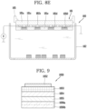
- FIG. 6 is a conceptual diagram showing an example of a self-assembly apparatus of a semiconductor light emitting diode according to the present invention
- FIG. 7 is a block diagram of the self-assembly apparatus of FIG. 6
- FIGS. 8A to 8E are conceptual views showing a process of self-assembling a semiconductor light emitting diode using the self-assembly apparatus of FIG. 6
- FIG. 9 is a conceptual diagram for describing the semiconductor light emitting diode of FIGS. 8A to 8E .
- a self-assembly apparatus 160 of the present invention may include a fluid chamber 162, a magnet 163 and a position control unit 164.
- the fluid chamber 162 has a space for accommodating a plurality of semiconductor light emitting diodes.
- the space may be filled with a fluid, and the fluid may include water or the like as an assembly solution.
- the fluid chamber 162 may be a water tank and may be configured in an open type.
- the present disclosure is not limited thereto, and the fluid chamber 162 may be of a closed type in which the space is a closed space.
- the board 161 may be disposed in the fluid chamber 162 such that an assembly surface on which the semiconductor light emitting diodes 150 are assembled faces downward.
- the board 161 may be transferred to an assembly position by a transfer device, and the transfer device may include a stage 165 on which the board is mounted. The position of the stage 165 is controlled by the control unit, and through this, the board 161 may be transferred to the assembly position.
- the assembly surface of the board 161 faces the bottom of the fluid chamber 150.
- the assembly surface of the board 161 is disposed to be immersed in the fluid in the fluid chamber 162. Accordingly, the semiconductor light emitting diode 150 moves to the assembly surface in the fluid.
- the board 161 is an assembly board in which an electric field is able to be formed, and may include a base portion 161a, a dielectric layer 161b, and a plurality of electrodes 161c.
- the base portion 161a may be formed of an insulating material, and the plurality of electrodes 161c may be a thin or thick bi-planar electrode patterned on one surface of the base portion 161a.
- the electrode 161c may be formed of, for example, a stack of Ti/Cu/Ti, Ag paste, and ITO.
- the dielectric layer 161b may be formed of an inorganic material such as SiO2, SiNx, SiON, Al2O3, TiO2, HfO2, or the like. Alternatively, the dielectric layer 161b may be comprised of a single layer or a multi-layer as an organic insulator. The dielectric layer 161b may have a thickness of several tens of nm to several ⁇ m.
- the board 161 includes a plurality of cells 161d separated by barrier ribs.
- the cells 161d are sequentially arranged in one direction and may be made of a polymer material.
- the barrier ribs 161e defining the cells 161d are shared with the neighboring cells 161d.
- the barrier ribs 161e may protrude from the base portion 161a, and the cells 161d may be sequentially arranged along one direction by the barrier ribs 161e. More specifically, the cells 161d are sequentially arranged in the column and row directions, respectively, and may have a matrix structure.
- the cell 161d may have a groove for accommodating the semiconductor light emitting diode 150 and the groove may be a space defined by the barrier ribs 161e.
- the shape of the groove may be the same as or similar to that of the semiconductor light emitting diode.
- the groove may have a rectangular shape.
- the groove formed in the cells may have a circular shape.
- each of the cells is configured to accommodate a single semiconductor light emitting diode. That is, one semiconductor light emitting diode is accommodated in one cell.
- the plurality of electrodes 161c may include a plurality of electrode lines disposed at the bottom of each of the cells 161d, and the plurality of electrode lines may extend to adjacent cells.
- the plurality of electrodes 161c are disposed below the cells 161d, and different polarities are applied to the electrodes 161c to generate an electric field in the cells 161d.
- the dielectric layer may form the bottom of the cells 161d while the dielectric layer is covering the plurality of electrodes 161c.
- an electric field is formed, and the semiconductor light emitting diodes may be inserted into the cells 161d due to the electric field.
- the electrodes of the board 161 are electrically connected to a power supply device 171.
- the power supply device 171 may apply power to the plurality of electrodes to generate the electric field.
- the self-assembly apparatus may include a magnet 163 for applying a magnetic force to the semiconductor light emitting diodes.
- the magnet 163 is spaced apart from the fluid chamber 162 to apply a magnetic force to the semiconductor light emitting diodes 150.
- the magnet 163 may be disposed to face the opposite surface of the assembly surface of the board 161, and the position of the magnet is controlled by the position control unit 164 connected to the magnet 163.
- the semiconductor light emitting diode 1050 may include a magnetic material to move in the fluid due to the magnetic field of the magnet 163.
- a semiconductor light emitting diode including a magnetic material may include a first conductivity type electrode 1052, a second conductivity type electrode 1056, a first conductivity type semiconductor layer 1053 on which the first conductivity type electrode 1052 is disposed, a second conductivity type semiconductor layer 1055 on which the second conductivity type electrode 1056 is disposed, the second conductivity type semiconductor layer 1055 overlapping the first conductivity type semiconductor layer 1052 and an active layer 1054 disposed between the first and second conductivity type semiconductor layers 1053 and 1055.
- the first conductivity type may be p-type
- the second conductivity type may be n-type
- the semiconductor light emitting diode having no active layer may be used.
- the first conductivity type electrode 1052 may be generated after the semiconductor light emitting diode is assembled to the wiring board through self-assembly of the semiconductor light emitting diode.
- the second conductivity type electrode 1056 may include the magnetic material.
- the magnetic material may mean a magnetic metal.
- the magnetic material may be Ni, SmCo, or the like, and as another example, may include a material corresponding to at least one of Gd-based, La-based, and Mn-based materials.
- the magnetic material may be provided in the second conductivity type electrode 1056 in the form of particles.
- the conductivity type electrode including a magnetic material may have one layer formed of a magnetic material.
- the second conductivity type electrode 1056 of the semiconductor light emitting diode 1050 may include a first layer 1056a and a second layer 1056b.
- the first layer 1056a may include a magnetic material
- the second layer 1056b may include a metal material rather than a magnetic material.
- the first layer 1056a including a magnetic material may be disposed to contact the second conductivity type semiconductor layer 1055.
- the first layer 1056a is disposed between the second layer 1056b and the second conductivity type semiconductor layer 1055.
- the second layer 1056b may be a contact metal connected to the second electrode of the wiring board.
- the present disclosure is not necessarily limited thereto, and the magnetic material may be disposed on one surface of the first conductivity type semiconductor layer.
- the self-assembly apparatus is provided with a magnet handler that is movable automatically or manually in the x, y, and z axes on the upper portion of the fluid chamber, or a motor capable of rotating the magnet 163.
- the magnet handler and the motor may constitute the position control unit 164. Through this, the magnet 163 may rotate in a horizontal direction with the board 161, clockwise or counterclockwise direction.
- a bottom plate 166 having a light-transmitting property may be formed in the fluid chamber 162, and the semiconductor light emitting diodes may be disposed between the bottom plate 166 and the board 161.
- An image sensor 167 may be disposed to face the bottom plate 166 to monitor the inside of the fluid chamber 162 through the bottom plate 166.
- the image sensor 167 is controlled by the control unit 172 and may include an inverted type lens, a CCD and the like to observe the assembly surface of the board 161.
- the self-assembly apparatus described above is configured to use a combination of a magnetic field and an electric field, and when using this, the semiconductor light emitting diodes may be seated at predetermined positions on the board due to an electric field while moving by a change in the position of the magnet.
- a plurality of semiconductor light emitting diodes 1050 including a magnetic material are formed through the process described with reference to FIGS. 5A to 5C .
- a magnetic material may be deposited on the semiconductor light emitting diode.
- the board 161 is transferred to an assembly position, and the semiconductor light emitting diodes 1050 are put into the fluid chamber 162 ( FIG. 8A ).
- the assembly position of the board 161 may be a position in which the board 161 is to be disposed in the fluid chamber 162 such that the assembly surface of the board 161 on which the semiconductor light emitting diodes 1050 are to be assembled faces downward.
- some of the semiconductor light emitting diodes 1050 may sink to the bottom of the fluid chamber 162 and some may float in the fluid.
- the bottom plate 166 having a light-transmitting property is provided in the fluid chamber 162, and some of the semiconductor light emitting diodes 1050 may sink to the bottom plate 166.
- a magnetic force is applied to the semiconductor light emitting diodes 1050 such that the semiconductor light emitting diodes 1050 vertically float in the fluid chamber 162 ( FIG. 8B ).
- the semiconductor light emitting diodes 1050 may float toward the board 161 in the fluid.
- the original position may be a position deviated from the fluid chamber 162.
- the magnet 163 may be made of an electromagnet. In this case, electricity is supplied to the electromagnet to generate an initial magnetic force.
- the separation distance between the assembly surface of the board 161 and the semiconductor light emitting diodes 1050 may be controlled.
- the separation distance is controlled using the weight, buoyancy, and magnetic force of the semiconductor light emitting diodes 1050.
- the separation distance may be several millimeters to several tens of micrometers from the outermost edge of the board.
- a magnetic force is applied to the semiconductor light emitting diodes 1050 such that the semiconductor light emitting diodes 1050 move in one direction in the fluid chamber 162.
- the magnet 163 it is possible to move the magnet 163 in a direction horizontal to the board, clockwise or counterclockwise ( FIG. 8C ).
- the semiconductor light emitting diodes 1050 move in a direction parallel to the board 161 from positions spaced apart from the board 161 due to the magnetic force.
- an electric field is applied to guide the semiconductor light emitting diodes 1050 to preset positions such that the semiconductor light emitting diodes 1050 are seated in the preset positions of the board 161 while the semiconductor light emitting diodes 1050 are moving ( FIG. 8C ).
- the semiconductor light emitting diodes 1050 may move in a direction perpendicular to the board 161 due to the electric field, and be then seated in the preset positions of the board 161.
- an electric field is generated by supplying power to the bi-planar electrode of the board 161 to enable assembly to be made only at preset positions. That is, the semiconductor light emitting diodes 1050 are self-assembled at assembly positions of the board 161 by using the selectively generated electric field. To this end, cells in which the semiconductor light emitting diodes 1050 are inserted may be provided in the board 161.
- a process of unloading the board 161 is performed, and the assembly process is finished.
- the board 161 is an assembly board
- a postprocess for realizing a display device by transferring the semiconductor light emitting diodes arranged as described above to a wiring board may be performed.
- the magnet 163 may be moved in a direction away from the board 161 such that the semiconductor light emitting diodes 1050 remaining in the fluid chamber 162 fall to the bottom of the fluid chamber 162 ( FIG. 8D ).
- the semiconductor light emitting diodes 1050 remaining in the fluid chamber 162 may fall to the bottom of the fluid chamber 162.
- the recovered semiconductor light emitting diodes 1050 may be reused.
- the self-assembly apparatus and method described above may use a magnetic field to enable distant parts to congregate near a predetermined assembly site and apply a separate electric field to the assembly site such that the parts are selectively assembled only to the assembly site in order to increase the assembly yield in fluidic assembly.
- the assembly board is placed on the upper portion of the water tank and the assembly surface is directed downward to minimize the effect of gravity due to the weight of the parts and prevent non-specific binding to eliminate defects. That is, to increase the transfer yield, the assembly board is placed on the upper portion to minimize the effect of gravity or frictional force, and to prevent non-specific binding.
- a large number of semiconductor light emitting diodes may be assembled at once.
- the present invention it is possible to pixelate a large amount of semiconductor light emitting diodes on a small-sized wafer and then transfer the semiconductor light emitting diodes to a large-area substrate. Through this, it is possible to manufacture a large-area display device at a low cost.
- the display apparatus 2000 described in this specification may be implemented in a passive matrix method (hereinafter, PM method) or an active matrix method (hereinafter referred to as AM method).
- PM method passive matrix method
- AM method active matrix method
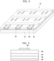
- FIG. 10 is a conceptual diagram showing a display device according to an embodiment of the present invention.
- the display device 2000 includes assembled electrodes 2020, a dielectric layer 2030, a semiconductor light emitting diode 2050 assembled in a cell 2040, and a partition wall portion 2060, a solder portion 2070, a first wiring electrode 2080, and the like, on a base portion 2010.
- the base portion 2010 may be a rigid substrate such as glass, sapphire, silicon, or the like. In another embodiment, the base portion 2010 may be a flexible substrate including a polymer material.
- polymer material for example, a material including flexible and insulating PI (polyimide), PEN (polyethylene naphthalate), PET (polyethylene terephthalate), or the like may be used.
- PI polyimide
- PEN polyethylene naphthalate
- PET polyethylene terephthalate
- Assembled electrodes 2020 extending in one direction may be formed on the base portion 2010.
- the assembled electrodes 2020 may be formed to a thickness of several hundred nm.
- the assembled electrodes 2020 may be configured to form an electric field during self-assembly. Specifically, a voltage signal may be applied to the assembled electrodes 2020 and transmitted in the extension direction.
- the assembled electrodes 2020 may be formed of a non-resistive metal corresponding to any one of Al, Mo, Cu, Ag, and Ti, or an alloy selected from these.
- the metal forming the assembled electrodes 2020 is not limited to those described above.
- a dielectric layer 2030 may be formed on the base portion 2010 to cover the assembled electrodes 2020.
- the dielectric layer 2030 may be made of an inorganic insulating material such as SiO 2 , SiN x , SiON, Al 2 O 3 , TiO 2 , HfO 2 , or the like.
- the dielectric layer 2030 may be formed as a single layer or as a multi-layer.
- the dielectric layer 2030 may be formed as a multi-layer including a first dielectric layer covering the wiring electrode and the second dielectric layer covering the assembled electrode 2020 to electrically insulate the assembled electrode 2020 and the wiring electrode.
- a partition wall portion 2060 may be stacked on the dielectric layer 2030 while forming a plurality of cells 2040.
- the plurality of cells 2040 may be formed in a matrix arrangement, and the semiconductor light emitting diodes 2050 may be seated inside the cells 2040 through self-assembly.
- the semiconductor light emitting diodes 2050 transferred to the substrate by the self-assembly method may be formed in a symmetrical structure, for example, may be formed in a circular shape.
- the partition wall portion 2060 may be formed of an organic insulating material (for example, PAC) made of a polymer material or an inorganic insulating material such as SiO 2 or SiN x .
- organic insulating material for example, PAC
- SiO 2 or SiN x an organic insulating material
- a planarization layer (not shown) for electrically insulating the semiconductor light emitting diode 2050 from the wiring electrode while planarizing the upper surface of the semiconductor light emitting diode 2050 seated in the cell 2040 may be included.
- the display device 2000 includes semiconductor light emitting diodes 2050 that emit light of different colors.
- the display device 2000 may include semiconductor light emitting diodes 2050 emitting blue, green, and red light.
- the display device 2000 is characterized in that it has a structure capable of simultaneously self-assembling the semiconductor light emitting diodes 2050 that emit light of different colors to a substrate.
- the semiconductor light emitting diodes 2050 that emit light of different colors includes recessed portions 2050R having different shapes on one surface.
- the substrate includes a solder portion 2070 protruding from the bottom surface of the cell 2040 to correspond to the recessed portion 2050R of the semiconductor light emitting diode 2050 which is seated (or which will be seated) on the cell 2040.
- the semiconductor light emitting diode 2050 may be a vertical semiconductor light emitting diode 2050.
- the vertical semiconductor light emitting diode 2050 can form the active layer 2030 wider than that of the horizontal semiconductor light emitting diode, and thus has an excellent advantage in terms of luminous efficiency. In addition, it is advantageous for miniaturization of the semiconductor light emitting diode 2050.
- FIG. 15 is a conceptual diagram showing a semiconductor light emitting diode according to an embodiment of the present invention.
- the semiconductor light emitting diode 2050 may include a first conductivity type electrode 2051, a first conductivity type semiconductor layer 2052 formed on the first conductivity type electrode 2051, an active layer 2053 formed on the first conductivity type semiconductor layer 2052, a second conductivity type semiconductor layer 2054 formed on the active layer 2053, a second conductivity type electrode 2055 formed on the second conductivity type semiconductor layer 2054, and an undoped semiconductor layer 2056.
- the first conductivity type electrode 2051 may be formed as a transparent electrode as a side from which light generated in the active layer 2053 is emitted.
- the first conductivity type electrode 2051 may be formed of indium tin oxide (ITO), Al-doped zinc oxide (AZO), F-doped tin oxide (FTO), or the like.
- the undoped semiconductor layer 2056 may be a layer that is not removed when the semiconductor light emitting diodes 2050 grown on the growth substrate are separated from the growth substrate during the manufacturing process of the semiconductor light emitting diode 2050.
- semiconductor light emitting diodes 2050 from which the undoped semiconductor layer 2056 is removed are used for self-assembly.
- the weight of the semiconductor light emitting diode 2050 itself increases, thereby increasing the assembly speed.
- the undoped semiconductor layer 2056 may include a recessed portion 2050R.
- the recessed portion 2050R may be formed to pass through the undoped semiconductor layer 2056, and the recessed portion 2050R included in the semiconductor light emitting diodes 2050 emitting light of different colors from each other may be formed by etching different regions of the undoped semiconductor layer 2056.
- the recessed portion 2050R may be formed by etching up to a portion of the second conductivity type semiconductor layer 2054 to form an ohmic.
- the second conductivity type electrode 2055 and the undoped semiconductor layer 2056 may be formed in different regions on the second conductivity type semiconductor layer 2054.
- the second conductivity type electrode 2055 may be formed on the region of the second semiconductor layer 2054 overlapping the bottom surface of the recessed portion 2050R. Specifically, the second conductivity type electrode 2055 may be formed along the pattern of the recessed portion 2050R.
- the second conductivity type electrode 2055 may further include a magnetic layer 2055b to be induced by a magnetic force during self-assembly.
- the second conductivity type electrode 2055 may include a metal layer 2055a and a magnetic layer 2055b for ohmic contact.
- the magnetic layer 2055b may be formed of a metal material such as Cr, Ti, or the like in order to improve adhesion to the metal layer 2055a.
- solder portion 2070 formed on the base portion 2010 and coupled to the recessed portion 2050R can be formed of an element selected from Sn, In, Pb, Bi, Cd, and Zn, an element having a similar melting point to that of the element, or composite of elements.
- solder portion 2070 may be formed to have a thickness greater than that of the undoped semiconductor layer 2056 based on the stacking direction of the semiconductor light emitting diode 2050.
- the solder portion 2070 may further include a magnetic layer.
- the solder portion 2070 includes a magnetic layer, when a magnetic force acts between the solder portion 2070 and the semiconductor light emitting diode 2050 to remove the fluid contained in the chamber after self-assembly, it is possible to prevent the semiconductor light emitting diode 2050 from being separated from the cell 2040 by the flow of the fluid.
- the base portion 2010 may further include a wiring electrode (hereinafter, a first wiring electrode 2080) formed on the dielectric layer 2030.
- a wiring electrode hereinafter, a first wiring electrode 2080
- the first wiring electrode 2080 may be formed to contact the solder portion 2070 under the solder portion 2070, and thus the second conductivity type electrode 2055 and the first wiring electrode 2080 may be electrically connected to each other by coupling the recessed portion 2050R and the solder portion 2070. Meanwhile, a separate heat treatment step for electrical connection between the second conductivity type electrode 2055 and the first wiring electrode 2080 may be performed.
- first wiring electrode 2080 may be disposed on the dielectric layer 2030 so as not to overlap the assembled electrodes 2020.
- a second wiring electrode (not shown) electrically connected to the first conductivity type electrode 2051 of the semiconductor light emitting diode 2050 may be further included.
- the second wiring electrode may be formed under the semiconductor light emitting diode 2050 like the first wiring electrode 2080 or formed above the semiconductor light emitting diode 2050.
- FIG. 11 is a diagram showing a recessed portion of a semiconductor light emitting diode and a pattern of a solder portion of a substrate according to the embodiment of FIG. 10
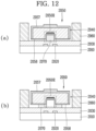
- FIG. 12 is a view showing a comparison of a state where a semiconductor light emitting diode is normally assembled on a substrate and a state where a semiconductor light emitting diode is incorrectly assembled on a substrate
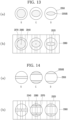
- FIGS. 13 and 14 are views showing a recessed portion of a semiconductor light emitting diode and a pattern of a solder portion of a substrate according to another embodiment of the present invention.
- the semiconductor light emitting diode 2050 emitting different colors includes recessed portions 2050R having different shapes.
- the semiconductor light emitting diode 2050 includes recessed portions 2050R formed at different positions on one surface, and in a bottom surface of the cell 2040, a solder portion 2070 having a shape corresponding to this, respectively is formed.
- the semiconductor light emitting diode 2050 may include a patterned recessed portion 2050R having different aspect ratios on one surface, and in the bottom surface of the cell 2040a, a solder portion 2070 having a shape corresponding to this, respectively may be formed.
- the semiconductor light emitting diode 2050 is seated in the cell 2040 including the solder portion 2070 that corresponds to the recessed portion 2050R to be capable of being strongly fixed inside the cell 2040 by the electric field formed by the assembled electrodes 2020.
- the bonding force (surface energy acting between the semiconductor light emitting diode 2050 and the solder portion 2070) is relatively weak, so that the semiconductor light emitting diode cannot be strongly fixed to the cell 2040 and may be easily detached from the cell 2040.
- the semiconductor light emitting diode 2050 may have vertical selectivity when assembling the cell 2040.
- the structure of the semiconductor light emitting diode 2050 for this will be described.
- FIGS. 16A and 16B are diagrams showing a semiconductor light emitting diode according to another embodiment of the present invention.
- the semiconductor light emitting diode 2050 may further include a passivation layer 2057 formed on the surface.
- the passivation layer 2057 may be formed to cover a portion of the surface of the semiconductor light emitting diode including the first conductivity type electrode 2051 on the other surface side of the semiconductor light emitting diode 2050, and, preferably, may be formed to extend from the top surface of the first conductivity type electrode 2051 to the side surface of the semiconductor light emitting diode 2050.
- the passivation layer 2057 may include an open hole for electrically connecting the first conductivity type electrode 2051 to the second wiring electrode.
- the area of one surface of the semiconductor light emitting diode 2050 including the recessed portion 2050R such that the recessed portion 2050R faces the bottom surface of the cell 2040 and the area of the other surface of the semiconductor light emitting diode 2050 on which the passivation layer 2057 is formed may be formed to be different from each other.
- the area of the passivation layer 2057 on the other side of the semiconductor light emitting diode 2050 may be patterned to be smaller than the area of the undoped semiconductor layer 2056 which is substantially in contact with the bottom surface of the cell 2040 on the one side of the semiconductor light emitting diode 2050.
- the area of the other surface of the semiconductor light emitting diode 2050 may be formed to be smaller than the area of one surface of the semiconductor light emitting diode 2050 by etching the circumferential portion except for the central region of the passivation layer 2057 formed on the other side of the semiconductor light emitting diode 2050.
- the area of the other surface of the semiconductor light emitting diode 2050 may be adjusted by etching a portion of the first conductivity type semiconductor layer 2052 and the first conductivity type electrode 2051 to form a mesa.
- the semiconductor light emitting diode 2050 may further include a metal film 2058 formed along an undoped semiconductor layer 2056 and a recessed portion 2050R on one side of the semiconductor light emitting diode 2050 such that the recessed portion 2050R faces the bottom surface of the cell 2040.
- the metal film 2058 may be formed of, for example, Ti, but is not limited thereto. Since the semiconductor light emitting diode 2050 includes the metal film 2058, the semiconductor light emitting diode 2050 can be easily guided into the assembly position, that is, into the cell 2040.
- the display device 2000 has the effect of being able to perform self-assembly by simultaneously putting the semiconductor light emitting diodes 2050 emitting light of different colors into the fluid chamber.
- the semiconductor light emitting diodes 2050 are seated at positions where the solder portions 2070 having a pattern corresponding to the recessed parts 2050R formed on one surface are formed, in order to self-assemble the semiconductor light emitting diodes 2050 at the same time., there is no need to manufacture different sizes or shapes of the semiconductor light emitting diodes 2050 that emit light of different colors.
- the semiconductor light emitting diode 2050 may be connected to a wiring electrode through a bonding of the recessed portion 2050R and the solder portion 2070, and the semiconductor light emitting diode 2050 seated in the cell 2040 is stably fixed to the substrate by the magnetic layer included in the solder portion 2070.
Landscapes
- Led Devices (AREA)
- Led Device Packages (AREA)
Claims (11)
- Anzeigevorrichtung, umfassend:einen Basisabschnitt (2010);zusammengesetzte Elektroden (2020), die sich in einer Richtung auf dem Basisabschnitt (2010) erstrecken;eine dielektrische Schicht (2030) zum Bedecken der zusammengesetzten Elektroden (2020);einen Trennwandabschnitt (2060) auf der dielektrischen Schicht (2030) unter Bildung einer Vielzahl von Zellen (2040); undeine Vielzahl von Halbleiter-Leuchtdioden (2050), die in der Vielzahl von jeweiligen Zellen (2040) sitzen und Licht verschiedener Farben emittieren,wobei die Vielzahl von Halbleiter-Leuchtdioden (2050), die verschiedene Farben emittieren, vertiefte Abschnitte (2050R) mit unterschiedlichen Formen auf einer Fläche davon aufweisen, undwobei eine untere Fläche der Vielzahl von Zellen (2040) einen Lötabschnitt (2070) enthält, der vorsteht, um dem vertieften Abschnitt (2050R) der Vielzahl von Halbleiter-Leuchtdioden (2050) zu entsprechen, die in der Vielzahl von jeweiligen Zellen (2040) sitzen.
- Anzeigevorrichtung nach Anspruch 1, wobei eine Halbleiter-Leuchtdiode (2050) aus der Vielzahl von Halbleiterschichten umfasst:eine Elektrode (2051) vom einem ersten Leitfähigkeitstyp;eine Halbleiterschicht (2052) vom ersten Leitfähigkeitstyp auf der Elektrode (2051) vom ersten Leitfähigkeitstyp;eine aktive Schicht (2053) auf der Halbleiterschicht (2052) vom ersten Leitfähigkeitstyp;eine Halbleiterschicht (2054) von einem zweiten Leitfähigkeitstyp auf der aktiven Schicht (2053);eine Elektrode (2055) vom zweiten Leitfähigkeitstyp auf der Halbleiterschicht (2054) vom zweiten Leitfähigkeitstyp; undeine undotierte Halbleiterschicht (2056) auf der Halbleiterschicht (2054) vom zweiten Leitfähigkeitstyp.
- Anzeigevorrichtung nach Anspruch 2,wobei ein vertiefter Abschnitt (2050R) für die Halbleiter-Leuchtdiode (2050) aus den vertieften Abschnitten (2050R) durch die undotierte Halbleiterschicht (2056) dringt, undwobei die Elektrode (2055) vom zweiten Leitfähigkeitstyp aus dem Gesamtbereich der Halbleiterschicht (2054) vom zweiten Leitfähigkeitstyp in einem Bereich ausgebildet ist, der sich von einem Bereich unterscheidet, in dem die undotierte Halbleiterschicht (2056) ausgebildet ist.
- Anzeigevorrichtung nach Anspruch 3,
wobei die Halbleiter-Leuchtdiode (2050) ferner eine Passivierungsschicht enthält, die einen Teil einer Fläche der Halbleiter-Leuchtdiode (2050) einschließlich der Elektrode (2051) vom ersten Leitfähigkeitstyp auf einer anderen Seite der Halbleiter-Leuchtdiode (2050) bedeckt. - Anzeigevorrichtung nach Anspruch 4,
wobei die Passivierungsschicht auf der anderen Seite der Halbleiter-Leuchtdiode (2050) so strukturiert ist, dass sie kleiner ist als ein Bereich der undotierten Halbleiterschicht (2056), der auf der einen Seite der Halbleiter-Leuchtdiode (2050) ausgebildet ist. - Anzeigevorrichtung nach Anspruch 2,
wobei die Halbleiter-Leuchtdiode (2050) ferner eine Metallfolie enthält, die entlang der undotierten Halbleiterschicht (2056) und dem vertieft ausgeführten Abschnitt (2050R) auf der einen Seite der Halbleiter-Leuchtdiode (2050) ausgebildet ist. - Anzeigevorrichtung nach Anspruch 2,
wobei die Elektrode (2055) vom zweiten Leitfähigkeitstyp ferner eine magnetische Schicht enthält. - Anzeigevorrichtung nach Anspruch 7,
wobei der Lötabschnitt (2070) weiterhin eine magnetische Schicht enthält. - Anzeigevorrichtung nach Anspruch 2,
wobei der Lötabschnitt (2070) eine Dicke aufweist, die größer ist als die Dicke der undotierten Halbleiterschicht (2056), basierend auf einer Stapelrichtung der Halbleiter-Leuchtdiode (2050). - Anzeigevorrichtung nach Anspruch 1, ferner umfassend:eine erste Verdrahtungselektrode (2080) auf der dielektrischen Schicht (2030),wobei die erste Verdrahtungselektrode (2080) den Lötabschnitt (2070) unter dem Lötabschnitt (2070) kontaktiert und zwischen den zusammengesetzten Elektroden (2020) angeordnet ist.
- Anzeigevorrichtung nach Anspruch 1, wobei die abgerundete Form eine Kreisform, eine ovale Form und eine Ringform umfasst.
Applications Claiming Priority (2)
| Application Number | Priority Date | Filing Date | Title |
|---|---|---|---|
| KR1020200006103A KR102810557B1 (ko) | 2020-01-16 | 2020-01-16 | 반도체 발광소자를 이용한 디스플레이 장치 |
| PCT/KR2020/000983 WO2021145499A1 (ko) | 2020-01-16 | 2020-01-21 | 반도체 발광소자를 이용한 디스플레이 장치 |
Publications (3)
| Publication Number | Publication Date |
|---|---|
| EP4092747A1 EP4092747A1 (de) | 2022-11-23 |
| EP4092747A4 EP4092747A4 (de) | 2024-01-17 |
| EP4092747B1 true EP4092747B1 (de) | 2025-01-08 |
Family
ID=69783121
Family Applications (1)
| Application Number | Title | Priority Date | Filing Date |
|---|---|---|---|
| EP20914448.4A Active EP4092747B1 (de) | 2020-01-16 | 2020-01-21 | Anzeigevorrichtung mit lichtemittierendem halbleiterbauelement |
Country Status (4)
| Country | Link |
|---|---|
| US (1) | US12495649B2 (de) |
| EP (1) | EP4092747B1 (de) |
| KR (1) | KR102810557B1 (de) |
| WO (1) | WO2021145499A1 (de) |
Families Citing this family (17)
| Publication number | Priority date | Publication date | Assignee | Title |
|---|---|---|---|---|
| KR102888284B1 (ko) * | 2020-02-20 | 2025-11-19 | 엘지전자 주식회사 | 반도체 발광소자를 이용한 디스플레이 장치 |
| CN111540815B (zh) * | 2020-03-23 | 2025-02-14 | 重庆康佳光电科技有限公司 | 球形垂直微型led及其制造方法、显示面板及其转移方法 |
| US12512443B2 (en) | 2020-06-01 | 2025-12-30 | Lg Electronics Inc. | Display device manufacturing substrate, and method for manufacturing display device by using same |
| FR3111236A1 (fr) * | 2020-06-03 | 2021-12-10 | Aledia | Dispositif électronique pour capture ou émission d’une grandeur physique et procédé de fabrication |
| WO2022034932A1 (ko) * | 2020-08-10 | 2022-02-17 | 엘지전자 주식회사 | 디스플레이 장치 제조용 기판 및 이를 이용한 디스플레이 장치의 제조방법 |
| US12027648B2 (en) * | 2020-09-29 | 2024-07-02 | BOE MLED Technology Co., Ltd. | Light-emitting diode chip, display substrate and manufacturing method thereof |
| US20230378141A1 (en) * | 2020-10-13 | 2023-11-23 | Lg Electronics Inc. | Display device |
| EP4177972A4 (de) | 2020-10-19 | 2023-12-06 | Samsung Electronics Co., Ltd. | Anzeigemodul |
| WO2023157996A1 (ko) * | 2022-02-21 | 2023-08-24 | 엘지전자 주식회사 | 반도체 발광 소자 및 디스플레이 장치 |
| WO2023167350A1 (ko) * | 2022-03-04 | 2023-09-07 | 엘지전자 주식회사 | 반도체 발광 소자 및 디스플레이 장치 |
| WO2023191151A1 (ko) * | 2022-04-01 | 2023-10-05 | 엘지전자 주식회사 | 반도체 발광 소자 및 디스플레이 장치 |
| US20260033070A1 (en) * | 2022-07-20 | 2026-01-29 | Lg Electronics Inc. | Display device |
| US20260020396A1 (en) * | 2022-10-07 | 2026-01-15 | Lg Electronics Inc. | Display device |
| KR20250073188A (ko) * | 2022-10-11 | 2025-05-27 | 엘지전자 주식회사 | 반도체 발광소자를 포함하는 디스플레이 장치 |
| KR20240065670A (ko) * | 2022-11-07 | 2024-05-14 | 엘지디스플레이 주식회사 | 발광 소자 및 발광 소자를 포함하는 표시 장치 |
| KR20240103491A (ko) * | 2022-12-27 | 2024-07-04 | 엘지디스플레이 주식회사 | 표시 장치 및 표시 장치의 제조 방법 |
| KR20250076020A (ko) * | 2023-11-22 | 2025-05-29 | 엘지디스플레이 주식회사 | 발광 소자 및 이를 포함하는 표시 장치 |
Family Cites Families (12)
| Publication number | Priority date | Publication date | Assignee | Title |
|---|---|---|---|---|
| TWI631697B (zh) * | 2012-02-17 | 2018-08-01 | 財團法人工業技術研究院 | 發光元件及其製造方法 |
| US9825202B2 (en) * | 2014-10-31 | 2017-11-21 | eLux, Inc. | Display with surface mount emissive elements |
| KR102205693B1 (ko) | 2016-08-04 | 2021-01-21 | 엘지전자 주식회사 | 반도체 발광 소자를 이용한 디스플레이 장치 |
| KR102169274B1 (ko) | 2015-08-21 | 2020-10-23 | 엘지전자 주식회사 | 표시장치 |
| KR102393374B1 (ko) | 2015-08-31 | 2022-05-03 | 삼성디스플레이 주식회사 | 표시 장치 및 상기 표시 장치의 제조 방법 |
| KR102060471B1 (ko) * | 2017-02-01 | 2019-12-30 | 엘지전자 주식회사 | 반도체 발광 소자를 이용한 디스플레이 장치 및 이의 제조 방법 |
| KR102357645B1 (ko) * | 2017-05-30 | 2022-02-04 | 엘지전자 주식회사 | 반도체 발광소자를 이용한 디스플레이 장치 |
| WO2019132050A1 (ko) | 2017-12-26 | 2019-07-04 | 박일우 | Led 디스플레이 장치 및 그 제조 방법 |
| KR102105466B1 (ko) * | 2018-01-16 | 2020-04-28 | 엘지전자 주식회사 | 반도체 발광 소자를 이용한 디스플레이 장치 |
| KR102145193B1 (ko) * | 2018-04-19 | 2020-08-28 | 엘지전자 주식회사 | 반도체 발광 소자를 이용한 디스플레이 장치 및 이의 제조방법 |
| US10707377B2 (en) * | 2018-04-19 | 2020-07-07 | Lg Electronics Inc. | Display device using semiconductor light emitting device and method for manufacturing the same |
| KR102761865B1 (ko) * | 2019-08-28 | 2025-02-04 | 엘지전자 주식회사 | 마이크로 led를 이용한 디스플레이 장치 및 이의 제조 방법 |
-
2020
- 2020-01-16 KR KR1020200006103A patent/KR102810557B1/ko active Active
- 2020-01-21 US US17/793,295 patent/US12495649B2/en active Active
- 2020-01-21 EP EP20914448.4A patent/EP4092747B1/de active Active
- 2020-01-21 WO PCT/KR2020/000983 patent/WO2021145499A1/ko not_active Ceased
Also Published As
| Publication number | Publication date |
|---|---|
| EP4092747A4 (de) | 2024-01-17 |
| US20230352643A1 (en) | 2023-11-02 |
| WO2021145499A1 (ko) | 2021-07-22 |
| KR20200023316A (ko) | 2020-03-04 |
| EP4092747A1 (de) | 2022-11-23 |
| US12495649B2 (en) | 2025-12-09 |
| KR102810557B1 (ko) | 2025-05-22 |
Similar Documents
| Publication | Publication Date | Title |
|---|---|---|
| EP4092747B1 (de) | Anzeigevorrichtung mit lichtemittierendem halbleiterbauelement | |
| US12490555B2 (en) | Display device using semiconductor light-emitting element and manufacturing method thereof | |
| US12456713B2 (en) | Display apparatus using semiconductor light-emitting device | |
| US10607515B2 (en) | Display device using semiconductor light emitting device and method for manufacturing the same | |
| CN113228288B (zh) | 使用半导体发光器件的显示装置及其制造方法 | |
| US12469828B2 (en) | Display device using semiconductor light-emitting devices having a passivation layer | |
| US12520646B2 (en) | Display device using semiconductor light-emitting element | |
| EP4030481B1 (de) | Anzeigevorrichtung mit lichtemittierender halbleiterdiode | |
| EP3731274A1 (de) | Anzeigevorrichtung mit lichtemittierendem halbleiterbauelement und herstellungsverfahren davon | |
| EP4068366B1 (de) | Mikro-led verwendende anzeigevorrichtung | |
| US12080580B2 (en) | Method for manufacturing display device, and substrate for manufacturing display device | |
| KR20200014867A (ko) | 반도체 발광소자의 자가조립 장치 및 방법 | |
| KR20190122113A (ko) | 반도체 발광소자의 자가조립 장치 및 방법 | |
| US12356766B2 (en) | Display device using semiconductor light-emitting element seated in plurality of cells of barrier rib portion | |
| EP4105970A1 (de) | Vorrichtung und verfahren zur selbstmontage einer lichtemittierenden halbleitervorrichtung | |
| US12080689B2 (en) | Display device using semiconductor light-emitting elements and manufacturing method therefor | |
| US12453215B2 (en) | Display device having semiconductor light emitting diodes seated in a plurality of cells, and method for manufacturing the display device | |
| US12500212B2 (en) | Semiconductor light-emitting element supply device and supply method | |
| EP4105996A1 (de) | Anzeigevorrichtung mit verwendung eines lichtemittierenden halbleiterbauelements und verfahren zur herstellung davon | |
| EP4105995B1 (de) | Anzeigevorrichtung mit verwendung von lichtemittierenden halbleiterelementen und verfahren zur herstellung davon |
Legal Events
| Date | Code | Title | Description |
|---|---|---|---|
| STAA | Information on the status of an ep patent application or granted ep patent |
Free format text: STATUS: THE INTERNATIONAL PUBLICATION HAS BEEN MADE |
|
| PUAI | Public reference made under article 153(3) epc to a published international application that has entered the european phase |
Free format text: ORIGINAL CODE: 0009012 |
|
| STAA | Information on the status of an ep patent application or granted ep patent |
Free format text: STATUS: REQUEST FOR EXAMINATION WAS MADE |
|
| 17P | Request for examination filed |
Effective date: 20220815 |
|
| AK | Designated contracting states |
Kind code of ref document: A1 Designated state(s): AL AT BE BG CH CY CZ DE DK EE ES FI FR GB GR HR HU IE IS IT LI LT LU LV MC MK MT NL NO PL PT RO RS SE SI SK SM TR |
|
| DAV | Request for validation of the european patent (deleted) | ||
| DAX | Request for extension of the european patent (deleted) | ||
| REG | Reference to a national code |
Ref country code: DE Ref legal event code: R079 Free format text: PREVIOUS MAIN CLASS: H01L0027150000 Ipc: H01L0025075000 Ref document number: 602020044673 Country of ref document: DE |
|
| A4 | Supplementary search report drawn up and despatched |
Effective date: 20231214 |
|
| RIC1 | Information provided on ipc code assigned before grant |
Ipc: H01L 33/62 20100101ALI20231208BHEP Ipc: H01L 33/38 20100101ALI20231208BHEP Ipc: H01L 33/20 20100101ALI20231208BHEP Ipc: H01L 25/075 20060101AFI20231208BHEP |
|
| GRAP | Despatch of communication of intention to grant a patent |
Free format text: ORIGINAL CODE: EPIDOSNIGR1 |
|
| STAA | Information on the status of an ep patent application or granted ep patent |
Free format text: STATUS: GRANT OF PATENT IS INTENDED |
|
| INTG | Intention to grant announced |
Effective date: 20240809 |
|
| GRAS | Grant fee paid |
Free format text: ORIGINAL CODE: EPIDOSNIGR3 |
|
| GRAA | (expected) grant |
Free format text: ORIGINAL CODE: 0009210 |
|
| STAA | Information on the status of an ep patent application or granted ep patent |
Free format text: STATUS: THE PATENT HAS BEEN GRANTED |
|
| AK | Designated contracting states |
Kind code of ref document: B1 Designated state(s): AL AT BE BG CH CY CZ DE DK EE ES FI FR GB GR HR HU IE IS IT LI LT LU LV MC MK MT NL NO PL PT RO RS SE SI SK SM TR |
|
| REG | Reference to a national code |
Ref country code: GB Ref legal event code: FG4D |
|
| REG | Reference to a national code |
Ref country code: CH Ref legal event code: EP |
|
| REG | Reference to a national code |
Ref country code: DE Ref legal event code: R096 Ref document number: 602020044673 Country of ref document: DE |
|
| REG | Reference to a national code |
Ref country code: IE Ref legal event code: FG4D |
|
| REG | Reference to a national code |
Ref country code: LT Ref legal event code: MG9D |
|
| REG | Reference to a national code |
Ref country code: NL Ref legal event code: MP Effective date: 20250108 |
|
| REG | Reference to a national code |
Ref country code: AT Ref legal event code: MK05 Ref document number: 1758919 Country of ref document: AT Kind code of ref document: T Effective date: 20250108 |
|
| PG25 | Lapsed in a contracting state [announced via postgrant information from national office to epo] |
Ref country code: NL Free format text: LAPSE BECAUSE OF FAILURE TO SUBMIT A TRANSLATION OF THE DESCRIPTION OR TO PAY THE FEE WITHIN THE PRESCRIBED TIME-LIMIT Effective date: 20250108 |
|
| PG25 | Lapsed in a contracting state [announced via postgrant information from national office to epo] |
Ref country code: RS Free format text: LAPSE BECAUSE OF FAILURE TO SUBMIT A TRANSLATION OF THE DESCRIPTION OR TO PAY THE FEE WITHIN THE PRESCRIBED TIME-LIMIT Effective date: 20250408 |
|
| PG25 | Lapsed in a contracting state [announced via postgrant information from national office to epo] |
Ref country code: FI Free format text: LAPSE BECAUSE OF FAILURE TO SUBMIT A TRANSLATION OF THE DESCRIPTION OR TO PAY THE FEE WITHIN THE PRESCRIBED TIME-LIMIT Effective date: 20250108 |
|
| PG25 | Lapsed in a contracting state [announced via postgrant information from national office to epo] |
Ref country code: PL Free format text: LAPSE BECAUSE OF FAILURE TO SUBMIT A TRANSLATION OF THE DESCRIPTION OR TO PAY THE FEE WITHIN THE PRESCRIBED TIME-LIMIT Effective date: 20250108 |
|
| PG25 | Lapsed in a contracting state [announced via postgrant information from national office to epo] |
Ref country code: ES Free format text: LAPSE BECAUSE OF FAILURE TO SUBMIT A TRANSLATION OF THE DESCRIPTION OR TO PAY THE FEE WITHIN THE PRESCRIBED TIME-LIMIT Effective date: 20250108 |
|
| PG25 | Lapsed in a contracting state [announced via postgrant information from national office to epo] |
Ref country code: NO Free format text: LAPSE BECAUSE OF FAILURE TO SUBMIT A TRANSLATION OF THE DESCRIPTION OR TO PAY THE FEE WITHIN THE PRESCRIBED TIME-LIMIT Effective date: 20250408 Ref country code: IS Free format text: LAPSE BECAUSE OF FAILURE TO SUBMIT A TRANSLATION OF THE DESCRIPTION OR TO PAY THE FEE WITHIN THE PRESCRIBED TIME-LIMIT Effective date: 20250508 |
|
| PG25 | Lapsed in a contracting state [announced via postgrant information from national office to epo] |
Ref country code: HR Free format text: LAPSE BECAUSE OF FAILURE TO SUBMIT A TRANSLATION OF THE DESCRIPTION OR TO PAY THE FEE WITHIN THE PRESCRIBED TIME-LIMIT Effective date: 20250108 |
|
| PG25 | Lapsed in a contracting state [announced via postgrant information from national office to epo] |
Ref country code: LV Free format text: LAPSE BECAUSE OF FAILURE TO SUBMIT A TRANSLATION OF THE DESCRIPTION OR TO PAY THE FEE WITHIN THE PRESCRIBED TIME-LIMIT Effective date: 20250108 Ref country code: PT Free format text: LAPSE BECAUSE OF FAILURE TO SUBMIT A TRANSLATION OF THE DESCRIPTION OR TO PAY THE FEE WITHIN THE PRESCRIBED TIME-LIMIT Effective date: 20250508 |
|
| PG25 | Lapsed in a contracting state [announced via postgrant information from national office to epo] |
Ref country code: GR Free format text: LAPSE BECAUSE OF FAILURE TO SUBMIT A TRANSLATION OF THE DESCRIPTION OR TO PAY THE FEE WITHIN THE PRESCRIBED TIME-LIMIT Effective date: 20250409 Ref country code: BG Free format text: LAPSE BECAUSE OF FAILURE TO SUBMIT A TRANSLATION OF THE DESCRIPTION OR TO PAY THE FEE WITHIN THE PRESCRIBED TIME-LIMIT Effective date: 20250108 |
|
| PG25 | Lapsed in a contracting state [announced via postgrant information from national office to epo] |
Ref country code: AT Free format text: LAPSE BECAUSE OF FAILURE TO SUBMIT A TRANSLATION OF THE DESCRIPTION OR TO PAY THE FEE WITHIN THE PRESCRIBED TIME-LIMIT Effective date: 20250108 |
|
| REG | Reference to a national code |
Ref country code: CH Ref legal event code: PL |
|
| PG25 | Lapsed in a contracting state [announced via postgrant information from national office to epo] |
Ref country code: SE Free format text: LAPSE BECAUSE OF FAILURE TO SUBMIT A TRANSLATION OF THE DESCRIPTION OR TO PAY THE FEE WITHIN THE PRESCRIBED TIME-LIMIT Effective date: 20250108 |
|
| PG25 | Lapsed in a contracting state [announced via postgrant information from national office to epo] |
Ref country code: LU Free format text: LAPSE BECAUSE OF NON-PAYMENT OF DUE FEES Effective date: 20250121 |
|
| PG25 | Lapsed in a contracting state [announced via postgrant information from national office to epo] |
Ref country code: SM Free format text: LAPSE BECAUSE OF FAILURE TO SUBMIT A TRANSLATION OF THE DESCRIPTION OR TO PAY THE FEE WITHIN THE PRESCRIBED TIME-LIMIT Effective date: 20250108 |
|
| REG | Reference to a national code |
Ref country code: DE Ref legal event code: R097 Ref document number: 602020044673 Country of ref document: DE |
|
| PG25 | Lapsed in a contracting state [announced via postgrant information from national office to epo] |
Ref country code: DK Free format text: LAPSE BECAUSE OF FAILURE TO SUBMIT A TRANSLATION OF THE DESCRIPTION OR TO PAY THE FEE WITHIN THE PRESCRIBED TIME-LIMIT Effective date: 20250108 |
|
| PG25 | Lapsed in a contracting state [announced via postgrant information from national office to epo] |
Ref country code: MC Free format text: LAPSE BECAUSE OF FAILURE TO SUBMIT A TRANSLATION OF THE DESCRIPTION OR TO PAY THE FEE WITHIN THE PRESCRIBED TIME-LIMIT Effective date: 20250108 |
|
| PG25 | Lapsed in a contracting state [announced via postgrant information from national office to epo] |
Ref country code: BE Free format text: LAPSE BECAUSE OF NON-PAYMENT OF DUE FEES Effective date: 20250131 |
|
| PG25 | Lapsed in a contracting state [announced via postgrant information from national office to epo] |
Ref country code: CH Free format text: LAPSE BECAUSE OF NON-PAYMENT OF DUE FEES Effective date: 20250131 |
|
| PG25 | Lapsed in a contracting state [announced via postgrant information from national office to epo] |
Ref country code: EE Free format text: LAPSE BECAUSE OF FAILURE TO SUBMIT A TRANSLATION OF THE DESCRIPTION OR TO PAY THE FEE WITHIN THE PRESCRIBED TIME-LIMIT Effective date: 20250108 Ref country code: CZ Free format text: LAPSE BECAUSE OF FAILURE TO SUBMIT A TRANSLATION OF THE DESCRIPTION OR TO PAY THE FEE WITHIN THE PRESCRIBED TIME-LIMIT Effective date: 20250108 |
|
| REG | Reference to a national code |
Ref country code: BE Ref legal event code: MM Effective date: 20250131 |
|
| PG25 | Lapsed in a contracting state [announced via postgrant information from national office to epo] |
Ref country code: RO Free format text: LAPSE BECAUSE OF FAILURE TO SUBMIT A TRANSLATION OF THE DESCRIPTION OR TO PAY THE FEE WITHIN THE PRESCRIBED TIME-LIMIT Effective date: 20250108 |
|
| PG25 | Lapsed in a contracting state [announced via postgrant information from national office to epo] |
Ref country code: SK Free format text: LAPSE BECAUSE OF FAILURE TO SUBMIT A TRANSLATION OF THE DESCRIPTION OR TO PAY THE FEE WITHIN THE PRESCRIBED TIME-LIMIT Effective date: 20250108 |
|
| PLBE | No opposition filed within time limit |
Free format text: ORIGINAL CODE: 0009261 |
|
| STAA | Information on the status of an ep patent application or granted ep patent |
Free format text: STATUS: NO OPPOSITION FILED WITHIN TIME LIMIT |
|
| REG | Reference to a national code |
Ref country code: DE Ref legal event code: R079 Ref document number: 602020044673 Country of ref document: DE Free format text: PREVIOUS MAIN CLASS: H01L0025075000 Ipc: H10H0029240000 |
|
| 26N | No opposition filed |
Effective date: 20251009 |
|
| GBPC | Gb: european patent ceased through non-payment of renewal fee |
Effective date: 20250408 |
|
| PG25 | Lapsed in a contracting state [announced via postgrant information from national office to epo] |
Ref country code: GB Free format text: LAPSE BECAUSE OF NON-PAYMENT OF DUE FEES Effective date: 20250408 |
|
| PGFP | Annual fee paid to national office [announced via postgrant information from national office to epo] |
Ref country code: FR Payment date: 20251209 Year of fee payment: 7 |
|
| PG25 | Lapsed in a contracting state [announced via postgrant information from national office to epo] |
Ref country code: IE Free format text: LAPSE BECAUSE OF NON-PAYMENT OF DUE FEES Effective date: 20250121 |
|
| PG25 | Lapsed in a contracting state [announced via postgrant information from national office to epo] |
Ref country code: IT Free format text: LAPSE BECAUSE OF FAILURE TO SUBMIT A TRANSLATION OF THE DESCRIPTION OR TO PAY THE FEE WITHIN THE PRESCRIBED TIME-LIMIT Effective date: 20250108 |
|
| PGFP | Annual fee paid to national office [announced via postgrant information from national office to epo] |
Ref country code: DE Payment date: 20251208 Year of fee payment: 7 |