EP4030481B1 - Anzeigevorrichtung mit lichtemittierender halbleiterdiode - Google Patents
Anzeigevorrichtung mit lichtemittierender halbleiterdiode Download PDFInfo
- Publication number
- EP4030481B1 EP4030481B1 EP19945184.0A EP19945184A EP4030481B1 EP 4030481 B1 EP4030481 B1 EP 4030481B1 EP 19945184 A EP19945184 A EP 19945184A EP 4030481 B1 EP4030481 B1 EP 4030481B1
- Authority
- EP
- European Patent Office
- Prior art keywords
- light emitting
- semiconductor light
- layer
- emitting device
- conductivity type
- Prior art date
- Legal status (The legal status is an assumption and is not a legal conclusion. Google has not performed a legal analysis and makes no representation as to the accuracy of the status listed.)
- Active
Links
Images


Classifications
-
- H—ELECTRICITY
- H10—SEMICONDUCTOR DEVICES; ELECTRIC SOLID-STATE DEVICES NOT OTHERWISE PROVIDED FOR
- H10H—INORGANIC LIGHT-EMITTING SEMICONDUCTOR DEVICES HAVING POTENTIAL BARRIERS
- H10H20/00—Individual inorganic light-emitting semiconductor devices having potential barriers, e.g. light-emitting diodes [LED]
- H10H20/80—Constructional details
- H10H20/83—Electrodes
- H10H20/831—Electrodes characterised by their shape
- H10H20/8312—Electrodes characterised by their shape extending at least partially through the bodies
-
- H—ELECTRICITY
- H10—SEMICONDUCTOR DEVICES; ELECTRIC SOLID-STATE DEVICES NOT OTHERWISE PROVIDED FOR
- H10W—GENERIC PACKAGES, INTERCONNECTIONS, CONNECTORS OR OTHER CONSTRUCTIONAL DETAILS OF DEVICES COVERED BY CLASS H10
- H10W90/00—Package configurations
-
- H—ELECTRICITY
- H10—SEMICONDUCTOR DEVICES; ELECTRIC SOLID-STATE DEVICES NOT OTHERWISE PROVIDED FOR
- H10H—INORGANIC LIGHT-EMITTING SEMICONDUCTOR DEVICES HAVING POTENTIAL BARRIERS
- H10H20/00—Individual inorganic light-emitting semiconductor devices having potential barriers, e.g. light-emitting diodes [LED]
- H10H20/042—Superluminescent diodes
-
- H—ELECTRICITY
- H10—SEMICONDUCTOR DEVICES; ELECTRIC SOLID-STATE DEVICES NOT OTHERWISE PROVIDED FOR
- H10H—INORGANIC LIGHT-EMITTING SEMICONDUCTOR DEVICES HAVING POTENTIAL BARRIERS
- H10H20/00—Individual inorganic light-emitting semiconductor devices having potential barriers, e.g. light-emitting diodes [LED]
- H10H20/80—Constructional details
- H10H20/83—Electrodes
-
- H—ELECTRICITY
- H10—SEMICONDUCTOR DEVICES; ELECTRIC SOLID-STATE DEVICES NOT OTHERWISE PROVIDED FOR
- H10H—INORGANIC LIGHT-EMITTING SEMICONDUCTOR DEVICES HAVING POTENTIAL BARRIERS
- H10H20/00—Individual inorganic light-emitting semiconductor devices having potential barriers, e.g. light-emitting diodes [LED]
- H10H20/80—Constructional details
- H10H20/85—Packages
- H10H20/857—Interconnections, e.g. lead-frames, bond wires or solder balls
-
- H—ELECTRICITY
- H10—SEMICONDUCTOR DEVICES; ELECTRIC SOLID-STATE DEVICES NOT OTHERWISE PROVIDED FOR
- H10H—INORGANIC LIGHT-EMITTING SEMICONDUCTOR DEVICES HAVING POTENTIAL BARRIERS
- H10H29/00—Integrated devices, or assemblies of multiple devices, comprising at least one light-emitting semiconductor element covered by group H10H20/00
- H10H29/10—Integrated devices comprising at least one light-emitting semiconductor component covered by group H10H20/00
- H10H29/14—Integrated devices comprising at least one light-emitting semiconductor component covered by group H10H20/00 comprising multiple light-emitting semiconductor components
- H10H29/142—Two-dimensional arrangements, e.g. asymmetric LED layout
-
- H—ELECTRICITY
- H10—SEMICONDUCTOR DEVICES; ELECTRIC SOLID-STATE DEVICES NOT OTHERWISE PROVIDED FOR
- H10W—GENERIC PACKAGES, INTERCONNECTIONS, CONNECTORS OR OTHER CONSTRUCTIONAL DETAILS OF DEVICES COVERED BY CLASS H10
- H10W72/00—Interconnections or connectors in packages
- H10W72/01—Manufacture or treatment
- H10W72/019—Manufacture or treatment of bond pads
- H10W72/01931—Manufacture or treatment of bond pads using blanket deposition
- H10W72/01936—Manufacture or treatment of bond pads using blanket deposition in solid form, e.g. by using a powder or by laminating a foil
-
- H—ELECTRICITY
- H10—SEMICONDUCTOR DEVICES; ELECTRIC SOLID-STATE DEVICES NOT OTHERWISE PROVIDED FOR
- H10W—GENERIC PACKAGES, INTERCONNECTIONS, CONNECTORS OR OTHER CONSTRUCTIONAL DETAILS OF DEVICES COVERED BY CLASS H10
- H10W72/00—Interconnections or connectors in packages
- H10W72/01—Manufacture or treatment
- H10W72/0198—Manufacture or treatment batch processes
Definitions
- the present invention relates to a display device using a semiconductor light emitting device, and more particularly, to a display device using a semiconductor light emitting device having a size of several to several tens of ⁇ m.
- LCD liquid crystal displays
- OLED organic light emitting device
- micro-LED micro-LED display
- a micro-LED which is a semiconductor light emitting device having a diameter or cross-sectional area of 100 ⁇ m or less
- the display doesn't absorb light using a polarizing plate, and therefore very high efficiency can be provided.
- a large display requires millions of semiconductor light emitting devices, it is difficult to transfer the devices compared to other technologies.
- the technologies currently being developed for the transfer process include pick & place, Laser Lift-off (LLO), or self-assembly.
- the self-assembly method is a method in which the semiconductor light emitting device finds its own position in a fluid, and is the most advantageous method for implementing a large-screen display device.
- the self-assembly method there are a first method of directly assembling the semiconductor light emitting device to a final substrate on which wiring is formed and a second method of assembling the semiconductor light emitting device on a temporary substrate and transferring the semiconductor light emitting device to a final substrate on which wiring is formed through transfer.
- the first method is efficient in terms of process simplification and cost
- the second method has the advantage of adding a structure advantageous for self-assembly without limitation, and the two methods are selectively used.
- KR 2019 0085892 A relates to a display device using a micro light emitting diode and a manufacturing method thereof.
- KR 2019 0099164 A relates to a manufacturing method of a display device using a micro Light Emitting Diode and a substrate used for manufacturing the display device.
- An object of the present invention is to provide a display device using a semiconductor light emitting device having a structure capable of securing sufficient light emitting area while being assembled on an assembly substrate in a predetermined direction through a self-assembly method.
- Another object of the present invention is to provide a display device using a semiconductor light emitting device having improved light extraction efficiency.
- Another object of the present invention is to provide a display device using a semiconductor light emitting device having improved bonding strength between magnetic layers.
- the semiconductor light emitting device may include a second conductivity type semiconductor layer; an active layer formed on a part of the second conductivity type semiconductor layer; and a first conductivity type semiconductor layer formed on the active layer, and the magnetic layer is formed on the second conductivity type semiconductor layer.
- the semiconductor light emitting device may include a symmetry plane among arbitrary surfaces extending along a stacking direction of the semiconductor light emitting device and the symmetry plane may pass through a central portion of the semiconductor light emitting device.
- the symmetrical plane may extend in the same direction as the longitudinal direction of the magnetic layer.
- the semiconductor light emitting device may include a first conductive electrode formed on the first conductivity type semiconductor layer, and may selectively include a second conductive electrode formed on the second conductivity type semiconductor layer.
- the second conductive electrode may be formed on one surface of the second conductivity type semiconductor layer on which the active layer is formed, and the magnetic layer may be formed on other surface of the second conductivity type semiconductor layer opposite to the one surface.
- this embodiment may include a first wiring electrode connecting the first conductive electrodes of the semiconductor light emitting devices arranged in a first direction; and a second wiring electrode connecting the second conductive electrodes of the semiconductor light emitting devices arranged in a second direction.
- the magnetic layer may be formed on one surface of the second conductivity type semiconductor layer on which the active layer is formed, and may include a first wiring electrode connecting the first conductive electrodes of the semiconductor light emitting devices arranged in a first direction; and a second wiring electrode connecting the magnetic layers of the semiconductor light emitting devices arranged in a second direction.
- the semiconductor light emitting device includes only the first conductive electrode, at least one side of the magnetic layer may extend to an outer portion of the second conductivity type semiconductor layer.
- the second conductive electrode may be formed on an outer portion of the second conductivity type semiconductor layer.
- an area of one surface on a side of the first conductive electrode of the semiconductor light emitting device is smaller than an area of other surface facing the one surface.
- the semiconductor light emitting device may further include an auxiliary bonding layer between the magnetic layer and the second conductivity type semiconductor layer.
- each of the magnetic layer and the second conductivity type semiconductor layer may include a concave-convex structure on surfaces facing each other.
- the semiconductor light emitting device may further includes a reflective layer between the second conductive electrode and the second conductivity type semiconductor layer.
- the magnetic layer extending in the longitudinal direction included in the semiconductor light emitting device can be uniformly assembled in a direction perpendicular to the extending direction of the assembled electrodes disposed on the substrate, there is an effect that the assembly speed and assembly accuracy can be improved.
- the electrode wiring can be performed by directly connecting the magnetic layer or by etching only a minimum area, it is possible to secure a large light emitting area, thereby enabling miniaturization of the semiconductor light emitting device.
- the display device described in this specification may include a mobile phone, a smart phone, a laptop computer, a digital broadcasting terminal, a PDA (personal digital assistant), a PMP (portable multimedia player), a navigation, a slate PC, a tablet PC (tablet PC), an Ultrabook, a Digital TV, a desktop computer, etc.
- PDA personal digital assistant
- PMP portable multimedia player
- a navigation a slate PC
- tablet PC tablet PC
- Ultrabook Ultrabook
- a Digital TV a desktop computer
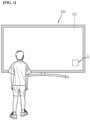
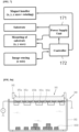
- FIG 1 is a conceptual diagram showing an embodiment of a display device using a semiconductor light emitting device of the present invention and FIG 2 is a partial enlarged view of part A of the display device of Figure 1 .
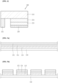
- FIG. 3 is an enlarged view of the semiconductor light emitting device of FIG. 2
- FIG. 4 is an enlarged view showing another embodiment of the semiconductor light emitting device of FIG. 2 .
- information processed by the control unit of the display apparatus 100 may be output from the display module 140.
- a closed-loop case 101 surrounding an edge of the display module may form a bezel of the display device.
- the display module 140 may include a panel 141 on which an image is displayed, the panel 141 may include a micro-sized semiconductor light emitting device 150 and a wiring board 110 on which the semiconductor light emitting device 150 is mounted.
- a wiring may be formed on the wiring board 110 to be connected to the n-type electrode 152 and the p-type electrode 156 of the semiconductor light emitting device 150.
- the semiconductor light emitting device 150 may be provided on the wiring board 110 as an individual pixel that emits light.
- the image displayed on the panel 141 is visual information, and is implemented by independently controlling the light emission of sub-pixels arranged in a matrix form through the wiring.
- a micro-LED Light Emitting Diode
- the micro-LED may be a light emitting diode formed in a small size of 100 micrometers or less.
- blue, red, and green colors are respectively provided in the light emitting region, and a unit pixel may be implemented by a combination thereof. That is, the unit pixel means a minimum unit for implementing one color, and at least three micro-LEDs may be provided in the unit pixel.
- the semiconductor light emitting device 150 may have a vertical structure.
- the semiconductor light-emitting device 150 may be implemented as a high-output light-emitting device that emits various types of light, including blue, by mainly using gallium nitride (GaN) and adding indium (In) and/or aluminum (Al) together.
- GaN gallium nitride
- Al aluminum
- This vertical semiconductor light emitting device includes a p-type electrode 156, a p-type semiconductor layer 155 formed on the p-type electrode 156, an active layer 154 formed on the p-type semiconductor layer 155, an n-type semiconductor layer 153 formed on the active layer 154, and an n-type electrode 152 formed on the n-type semiconductor layer 153.
- the lower p-type electrode 156 may be electrically connected to the p-electrode of the wiring board
- the upper n-type electrode 152 may be electrically connected to the n-electrode at the upper side of the semiconductor light emitting device.
- the vertical semiconductor light emitting device 150 has a great advantage in that it is possible to reduce the chip size because electrodes can be arranged up and down.
- the semiconductor light emitting device may be a flip chip type light emitting device.
- the semiconductor light emitting device 250 includes a p-type electrode 256, a p-type semiconductor layer 255 on which the p-type electrode 256 is formed, an active layer 254 formed on the p-type semiconductor layer 255, An n-type semiconductor layer 253 formed on the active layer 254, and an n-type electrode 252 spaced apart from the p-type electrode 256 in the horizontal direction on the n-type semiconductor layer 253.
- both the p-type electrode 256 and the n-type electrode 152 may be electrically connected to the p-electrode and the n-electrode of the wiring board under the semiconductor light emitting device.
- the vertical semiconductor light emitting device and the horizontal semiconductor light emitting device may be a green semiconductor light emitting device, a blue semiconductor light emitting device, or a red semiconductor light emitting device, respectively.
- the green semiconductor light emitting device and the blue semiconductor light emitting device Gallium nitride (GaN) may be mainly used, and indium (In) and/or aluminum (Al) may be added together, high-output light emitting devices emitting green light or blue light may be implemented.
- the semiconductor light emitting device may be a gallium nitride thin film formed in various layers such as n-Gan, p-Gan, AlGaN, InGan, etc.
- the p-type semiconductor layer may be P-type GaN, and the n-type semiconductor layer may be N-type GaN.
- the p-type semiconductor layer may be P-type GaAs, and the n-type semiconductor layer may be N-type GaAs.
- the p-type semiconductor layer may be P-type GaN doped with Mg on the p-electrode side
- the n-type semiconductor layer may be N-type GaN doped with Si on the n-electrode side.
- the above-described semiconductor light emitting devices may be semiconductor light emitting devices without an active layer.
- the semiconductor light emitting device grown on a wafer and formed through mesa and isolation is used as an individual pixel.
- the micro-sized semiconductor light emitting device 150 is to be transferred to a predetermined position on the substrate of the display panel on the wafer.
- There is a pick and place method as such a transfer technology but the success rate is low and a lot of time is required.
- there is a technique of transferring several devices at once using a stamp or a roll but there is a limit to the yield, so it is not suitable for a large screen display.
- the present invention proposes a new manufacturing method and manufacturing apparatus of a display device that can solve these problems.
- FIG. 5A to 5E are conceptual views for explaining a new process of manufacturing the above-described semiconductor light emitting device.
- a display device using a passive matrix (PM) type semiconductor light emitting device is exemplified.
- PM passive matrix
- AM active matrix
- a method of self-assembling a horizontal semiconductor light emitting device is exemplified, it is also applicable to a method of self-assembling a vertical semiconductor light emitting device.
- the first conductivity type semiconductor layer 153, the active layer 154, and the second conductivity type semiconductor layer 155 may be grown on the growth substrate 159, respectively ( FIG. 5A ).
- first conductivity type semiconductor layer 153 When the first conductivity type semiconductor layer 153 is grown, next, an active layer 154 is grown on the first conductivity type semiconductor layer 153, next, a second conductivity type semiconductor layer 155 is grown on the active layer 154. In this way, when the first conductivity type semiconductor layer 153, the active layer 154, and the second conductivity type semiconductor layer 155 may be sequentially grown, as shown in FIG. 5A , the first conductivity type semiconductor layer 153, the active layer 154, and the second conductivity type semiconductor layer 155 may form a stacked structure.
- the first conductivity type semiconductor layer 153 may be a p-type semiconductor layer
- the second conductivity type semiconductor layer 155 may be an n-type semiconductor layer.
- the present invention is not necessarily limited thereto, and examples in which the first conductivity type is n-type and the second conductivity type is p-type are also possible.
- the present embodiment exemplifies the case in which the active layer is present, a structure in which the active layer is not present is also possible in some cases as described above.
- the p-type semiconductor layer may be P-type GaN doped with Mg
- the n-type semiconductor layer may be N-type GaN doped with Si on the n-electrode side.
- the growth substrate 159 may be formed of a material having a light-transmitting property, for example, any one of sapphire (Al 2 O 3 ), GaN, ZnO, and AlO, but is not limited thereto.
- the growth substrate 1059 may be formed of a material suitable for semiconductor material growth, a carrier wafer. It may be formed of a material having excellent thermal conductivity, including a conductive substrate or an insulating substrate. For example, at least one of Si, GaAs, GaP, InP, and Ga 2 O 3 or a SiC substrate having higher thermal conductivity than a sapphire (Al 2 O 3 ) substrate may be used.
- the first conductivity type semiconductor layer 153, the active layer 154, and the second conductivity type semiconductor layer 155 are removed to form a plurality of semiconductor light emitting devices ((refer to FIG. 5B ).
- an isolation may be performed so that a plurality of light emitting devices form a light emitting device array. That is, the first conductivity type semiconductor layer 153, the active layer 154, and the second conductivity type semiconductor layer 155 may be vertically etched to form a plurality of semiconductor light emitting devices.
- the active layer 154 and the second conductivity type semiconductor layer 155 are partially removed in the vertical direction, so that the first conductivity type semiconductor layer 153 is exposed to the outside in a mesa process, thereafter, isolation of forming a plurality of semiconductor light emitting device arrays by etching the first conductivity type semiconductor layer may be performed.
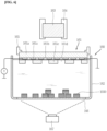
- FIG. 5E a step of seating the semiconductor light emitting devices 150 on a substrate in a chamber filled with a fluid is performed.
- the semiconductor light emitting devices 150 and the substrate are put in a chamber filled with a fluid, and the semiconductor light emitting devices may be self-assembled on the substrate 1061 using flow, gravity, surface tension, and the like.
- the substrate may be the assembly substrate 161.
- the substrate may be a wiring substrate.
- the substrate is provided as the assembly substrate 161 to exemplify that the semiconductor light emitting devices 1050 are seated.
- a magnetic material is disposed on the semiconductor light emitting device to move the semiconductor light emitting device using magnetic force, and the semiconductor light emitting device is seated at a preset position using an electric field during the movement process.
- the fluid chamber 162 may have a space for accommodating a plurality of semiconductor light emitting devices.
- the space may be filled with a fluid, and the fluid may include water as an assembly solution.
- the fluid chamber 162 may be a water tank, and may be configured as an open type.
- the present invention is not limited thereto, and the fluid chamber 162 may be of a closed type in which the space is a closed space.
- the substrate 161 may be disposed in the fluid chamber 162 so that the assembly surface on which the semiconductor light emitting devices 150 are assembled faces downward.
- the substrate 161 may be transferred to an assembly position by a transfer unit, and the transfer unit may include a stage 165 on which the substrate is mounted. The position of the stage 165 is adjusted by the controller, and through this, the substrate 161 can be transferred to the assembly position.
- the assembly surface of the substrate 161 faces the bottom of the fluid chamber 150 in the assembly position. As shown, the assembly surface of the substrate 161 is arranged to be immersed in the fluid in the fluid chamber 162. Accordingly, the semiconductor light emitting device 150 moves to the assembly surface in the fluid.
- the substrate 161 is an assembled substrate capable of forming an electric field, and may include a base portion 161a, a dielectric layer 161b, and a plurality of electrodes 161c.
- the dielectric layer 161b may be formed of an inorganic material such as SiO 2 , SiNx, SiON, Al 2 O 3 , TiO 2 , HfO 2 .
- the dielectric layer 161b may be formed of a single layer or a multi-layer as an organic insulator.
- the dielectric layer 161b may have a thickness of several tens of nm to several ⁇ ⁇ m.
- the plurality of electrodes 161c may include a plurality of electrode lines disposed at the bottom of each of the cells 161d, and the plurality of electrode lines may extend to adjacent cells.
- the electrodes of the substrate 161 are electrically connected to the power supply unit 171.
- the power supply unit 171 applies power to the plurality of electrodes to generate the electric field.
- the self-assembly apparatus may include a magnet 163 for applying a magnetic force to the semiconductor light emitting devices.
- the magnet 163 may be spaced apart from the fluid chamber 162 to apply a magnetic force to the semiconductor light emitting devices 150.
- the magnet 163 may be disposed to face the opposite surface of the assembly surface of the substrate 161, and the position of the magnet may be controlled by the position controller 164 connected to the magnet 163.
- the semiconductor light emitting device 1050 may include a magnetic material to move in the fluid by the magnetic field of the magnet 163.
- a semiconductor light emitting device including a magnetic material may include a first conductive electrode 1052, a second conductive electrode 1056, a first conductivity type semiconductor layer 1053 on which the first conductive electrode 1052 is disposed, a second conductivity type semiconductor layer 1055 overlapping the first conductivity type semiconductor layer 1052 and on which the second conductive electrode 1056 is disposed and an active layer 1054 disposed between the first and second conductivity type semiconductor layers 1053 and 1055.
- the first conductivity type may be a p-type
- the second conductivity type may be configured as an n-type, and vice versa.
- the semiconductor light emitting device without the active layer may be used.
- the first conductive electrode 1052 may be generated after the semiconductor light emitting device is assembled on the wiring board by self-assembly of the semiconductor light emitting device.
- the second conductive electrode 1056 may include the magnetic material.
- the magnetic material may mean a magnetic metal.
- the magnetic material may be Ni, SmCo, or the like, and as another example, may include a material corresponding to at least one of Gd-based, La-based, or Mn-based materials.
- the magnetic material may be provided in the second conductive electrode 1056 in the form of particles.
- a conductive electrode including a magnetic material one layer of the conductive electrode may be formed of a magnetic material.
- the first layer 1056a including a magnetic material may be disposed to contact the second conductivity type semiconductor layer 1055.
- the first layer 1056a may be disposed between the second layer 1056b and the second conductivity type semiconductor layer 1055.
- the second layer 1056b may be a contact metal connected to the second electrode of the wiring board.
- the present invention is not necessarily limited thereto, and the magnetic material may be disposed on one surface of the first conductivity type semiconductor layer.
- the self-assembly apparatus may include a magnet handler capable of automatically or manually moving the x, y, and z axes on the upper portion of the fluid chamber, or a motor capable of rotating the magnet 163.
- the magnet handler and the motor may constitute the position control unit 164. Through this, the magnet 163 may rotate in a horizontal direction, clockwise or counterclockwise direction with the substrate 161.
- the self-assembly device described above is made to use a combination of a magnetic field and an electric field, using this, the semiconductor light emitting devices can be seated at a predetermined position on the substrate by an electric field while the semiconductor light emitting devices are moved by a change in the position of the magnet.
- the assembly process using the self-assembly apparatus described above will be described in more detail.
- a plurality of semiconductor light emitting devices 1050 including a magnetic material are formed through the process described with reference to FIGS. 5A to 5C .
- a magnetic material may be deposited on the semiconductor light emitting device.
- the substrate 161 may be transferred to the assembly position, and the semiconductor light emitting devices 1050 may be put into the fluid chamber 162 ((refer to FIG. 8a ).
- the assembly position of the substrate 161 may be a position in which the assembly surface of the substrate 161 on which the semiconductor light emitting devices 1050 are assembled faces downward in the fluid chamber 162.
- some of the semiconductor light emitting devices 1050 may sink to the bottom of the fluid chamber 162 and some may float in the fluid.
- some of the semiconductor light emitting devices 1050 may sink to the bottom plate 166.
- a magnetic force may be applied to the semiconductor light emitting devices 1050 so that the semiconductor light emitting devices 1050 may vertically float in the fluid chamber 162 ((refer to FIG. 8B ).
- the spaced distance between the assembly surface of the substrate 161 and the semiconductor light emitting devices 1050 may be controlled.
- the spaced distance may be controlled using the weight, buoyancy, and magnetic force of the semiconductor light emitting devices 1050.
- the spaced distance may be several millimeters to several tens of micrometers from the outermost surface of the substrate.
- a magnetic force may be applied to the semiconductor light emitting devices 1050 so that the semiconductor light emitting devices 1050 may move in one direction in the fluid chamber 162.
- the magnet 163 may move in a direction parallel to the substrate, clockwise or counterclockwise ((refer to FIG. 8C ).
- the semiconductor light emitting devices 1050 may move in a direction parallel to the substrate 161 at a position spaced apart from the substrate 161 by the magnetic force.
- a step of inducing the semiconductor light emitting devices 1050 to the predetermined position by applying an electric field so as to be seated at a predetermined position of the substrate 161 is performed ((refer to FIG. 8C ).
- the semiconductor light emitting devices 1050 may move in a direction perpendicular to the substrate 161 to be seated at a preset position of the substrate 161 by the electric field.
- the semiconductor light emitting devices 1050 can be self-assembled at the assembly position of the substrate 161.
- cells in which the semiconductor light emitting devices 1050 are inserted may be provided on the substrate 161.
- the unloading process of the substrate 161 may proceed, and the assembly process may be completed.
- the substrate 161 is an assembly substrate
- a post-process for implementing a display device by transferring the semiconductor light emitting devices arranged as described above to a wiring board may be performed.
- the magnet 163 may be moved in a direction away from the substrate 161 so that the semiconductor light emitting elements 1050 remaining in the fluid chamber 162 fall to the bottom of the fluid chamber 162 ((refer to FIG. 8D ).
- the semiconductor light emitting devices 1050 remaining in the fluid chamber 162 may fall to the bottom of the fluid chamber 162.
- the recovered semiconductor light emitting devices 1050 can be reused.
- a magnetic field may be used to concentrate distant parts near a predetermined assembly site, and a separate electric field may be applied to the assembly site so that the parts are selectively assembled only at the assembly site.
- the assembly board may be placed on the upper part of the water tank and the assembly surface may be directed downward to minimize the effect of gravity due to the weight of the parts and prevent non-specific binding to eliminate defects. That is, to increase the transfer yield, the assembly substrate may be placed on the upper part to minimize the influence of gravity or frictional force, and non-specific binding can be prevented.
- the present invention it becomes possible to pixelate a large amount of semiconductor light emitting devices on a small-sized wafer and then transfer them to a large-area substrate. Through this, it is possible to manufacture a large-area display device at a low cost.
- the present invention relates to a display device using semiconductor light emitting devices including a magnetic layer extending in a longitudinal direction.
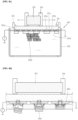
- FIG. 10 is a view showing a display device in which a semiconductor light emitting device according to an embodiment of the present invention is assembled.
- the display device 1000 includes a base portion 1010, assembly electrodes 1020, a dielectric layer 1030, a barrier wall portion 1040, a cell 1050 formed by the barrier wall 1040, and a semiconductor light emitting device 1060 seated in the cell 1050.
- the base portion 1010 may be a substrate on which the semiconductor light emitting device 1060 can be assembled, and may be, for example, a rigid substrate formed of a material such as sapphire, glass, or silicon, or a flexible substrate including polyimide (PI), etc.
- a rigid substrate formed of a material such as sapphire, glass, or silicon
- a flexible substrate including polyimide (PI), etc.
- the assembled electrodes 1020 may extend in one direction and may be formed on the base portion 1010 at predetermined intervals.
- a voltage for forming an electric field for self-assembly may be applied to the assembly electrodes 1020.
- an electric field may be formed between the assembled electrodes 1020.
- the dielectric layer 1030 is stacked on the base portion 1010 to cover the assembly electrodes 1020.
- the dielectric layer 1030 may be made of an inorganic material such as SiO 2 , SiNx, Al 2 O 3 , TiO 2 , HfO 2 , and the like, but is not limited thereto.
- the barrier wall portion 1040 is stacked on the dielectric layer 1030.
- the barrier wall portion 1040 is stacked on the dielectric layer 1030 while forming the cell 1050 overlapping at least a portion of the assembly electrode 1020 in the extending direction of the assembly electrode 1020.
- the barrier wall portion 1040 may be formed of an inorganic material such as SiO 2 or SiNx, or an organic material of a polymer material.
- the semiconductor light emitting device 1060 may be seated inside the cell 1050 under the influence of the electric field formed by the assembled electrodes 1020.
- the semiconductor light emitting device 1060 include a magnetic layer 1065 to enable self-assembly using a magnetic field and an electric field, and according to an embodiment of the present invention, the magnetic layer 1065 has a shape extended in longitudinal direction. Also, the semiconductor light emitting device 1060 may have a symmetrical structure.
- the semiconductor light emitting device 1060 is assembled in a certain direction as shown in FIG. 10 .
- the semiconductor light emitting device 1060 is assembled such that the longitudinal direction of the magnetic layer 1065 is perpendicular to the extending direction of the assembly electrodes 1020.
- the vertical may refer to a state in which an angle between the extension direction of the assembly electrodes 1020 and the longitudinal direction of the magnetic layer 1065 is 90° or substantially 90°.
- the polarized magnetic layer 1065 is in the most stable state when forming a vertical direction with respect to the assembled electrodes 1020, so the semiconductor light emitting devices 1060 may be assembled into the cell 1050 while having selectivity such that the longitudinal direction of the magnetic layer 1065 is perpendicular to the extending direction of the assembly electrodes 1020.
- the semiconductor light emitting device 1060 constituting the display device 1000 according to the embodiment of the present invention be manufactured in a symmetrical structure, and since the magnetic layer 1065 extending in the longitudinal direction is assembled in a predetermined direction, accordingly, self-assembly speed and assembly accuracy can be improved.
- the top and bottom selectivity of the semiconductor light emitting device 1060 may be determined by a contact area.
- the semiconductor light emitting device 1060 may be assembled such that a surface having a larger area is in contact with the bottom surface of the cell 1050. Accordingly, the semiconductor light emitting device 1060 may be manufactured so that an area of a surface opposite to a surface on which an electrode pad connected to a wiring electrode, which will be described later, is formed has a larger area than that of a surface on which the electrode pad is formed. That is, the semiconductor light emitting device 1060 may be manufactured so that one surface of the first conductive electrode 1064 has a smaller area than that of another surface facing the first conductive electrode 1064. To this end, a patterning or etching process for reducing a contact area on a specific surface of the semiconductor light emitting device 1060 may be performed.
- the semiconductor light emitting device 1060 may include a second conductivity type semiconductor layer 1061, an active layer 1062 formed on a portion of the second conductivity type semiconductor layer 1061, a first conductivity type semiconductor layer 1063 formed on the active layer 1062 and a first conductive electrode 1064 formed on the first conductivity type semiconductor layer 1063.
- the magnetic layer 1065 may be formed on the second conductivity type semiconductor layer 1061.
- the first conductive electrode 1064 may be an ITO or transparent electrode so that light emitted from the active layer 1062 can be transmitted to the upper surface of the semiconductor light emitting device 1060.
- the magnetic layer 1065 may be formed of a magnetic metal material, for example, Ni, accordingly, it is possible to replace the second conductive electrode 1066 and serve as a contact metal connected to the wiring electrode.
- the first conductivity type may be p-type
- the second conductivity type may be n-type, and vice versa.
- the semiconductor light emitting device 1060 may selectively include the second conductive electrode 1066 formed on the second conductivity type semiconductor layer 1061. Specifically, the semiconductor light emitting device 1060 may selectively include the second conductive electrode 1066 depending on the position (upper or lower) of the magnetic layer 1065, which will be described later.
- the semiconductor light emitting device 1060 may include at least one of symmetry planes among arbitrary surfaces extending along a stacking direction (or height direction) thereof, and the symmetry plane passing through a central portion C of the semiconductor light emitting device 1060
- the symmetrical plane may be a plane including a1 or a2 of FIGS. 11A and 14A , or a plane including an arbitrary line passing through the center C although not shown in the drawing.
- the semiconductor light emitting device 1060 may include the magnetic layer 1065 on the upper portion (first embodiment, FIGS. 11 to 13 ) or on the lower portion (second embodiment, Figs. 14 to 16 ).
- the second conductive electrode 1066 may be implemented by depositing a metal after mesa-etching a minimum area on the outer portion of the second conductivity type semiconductor layer 1061,
- the shape is not particularly limited, such as a circular shape or an oval shape.
Landscapes
- Led Devices (AREA)
- Led Device Packages (AREA)
Claims (14)
- Anzeigevorrichtung (1000), welche aufweist:einen Basisteil (1010);eine Vielzahl von Montageelektroden (1020), die sich in einer ersten Richtung erstrecken und in vorgegebenen Abständen an dem Basisteil (1010) angeordnet sind;eine dielektrische Schicht (1030), die auf dem Basisteil (1010) gestapelt ist, um die Montageelektroden (1020) abzudecken;einen Sperrwandabschnitt (1040), der auf der dielektrischen Schicht (1030) gestapelt ist und dabei eine Zelle (1050) bildet, die mindesten einen Abschnitt der Montageelektroden (1020) entlang der Erstreckungsrichtung der Montageelektrode (1020) überlagert; undeine Vielzahl von lichtemittierenden Halbleitervorrichtungen (1060), die in der Zelle (1050) angeordnet sind,wobei die lichtemittierenden Halbleitervorrichtungen (1060) eine magnetische Schicht (1065) in einer sich in der Längsrichtung erstreckenden Form umfassen,dadurch gekennzeichnet, dassdie Vielzahl von lichtemittierenden Halbleitervorrichtungen (1020) derart montiert sind, dass die Längsrichtung der magnetischen Schicht (1065) zu der ersten Richtung der Erstreckungsrichtung der Montageelektroden (1020) senkrecht ist.
- Anzeigevorrichtung (1000) nach Anspruch 1, wobei die lichtemittierende Halbleitervorrichtung (1060) Folgendes umfasst: eine Halbleiterschicht (1061) zweiten Leitfähigkeitstyps; eine aktive Schicht (1062), die auf einem Abschnitt der Halbleiterschicht (1061) zweiten Leitfähigkeitstyps angeordnet ist; und eine Halbleiterschicht (1063) ersten Leitfähigkeitstyps, die auf der aktiven Schicht (1062) angeordnet ist,
wobei die magnetische Schicht (1065) auf der Halbleiterschicht (1061) zweiten Leitfähigkeitstyps angeordnet ist. - Anzeigevorrichtung (1000) nach Anspruch 2, wobei die lichtemittierende Halbleitervorrichtung (1060) eine symmetrische Ebene unter beliebigen Oberflächen umfasst, die sich entlang einer Stapelrichtung der lichtemittierenden Halbleitervorrichtung (1060) erstreckt, und die symmetrische Ebene durch einen mittigen Abschnitt (C) der lichtemittierenden Halbleitervorrichtung (1060) läuft.
- Anzeigevorrichtung (1000) nach Anspruch 3, wobei sich die symmetrische Ebene in derselben Richtung erstreckt wie die Längsrichtung der magnetischen Schicht (1065).
- Anzeigevorrichtung (1000) nach einem von Anspruch 2 oder Anspruch 3, wobei die lichtemittierende Halbleitervorrichtung (1060) eine auf der Halbleiterschicht (1063) ersten Leitfähigkeitstyps angeordnete erste leitfähige Elektrode (1064) und eine auf der Halbleiterschicht (1061) zweiten Leitfähigkeitstyps angeordnete zweite leitfähige Elektrode (1066) umfasst.
- Anzeigevorrichtung (1000) nach Anspruch 5, wobei die zweite leitfähige Elektrode (1066) auf einer Oberfläche der Halbleiterschicht (1061) zweiten Leitfähigkeitstyps angeordnet ist, auf der die aktive Schicht (1062) angeordnet ist, undwobei die magnetische Schicht (1065) auf der anderen Oberfläche der Halbleiterschicht (1061) zweiten Leitfähigkeitstyps gegenüber von der einen Oberfläche angeordnet ist, undferner umfassend eine in einer ersten Richtung angeordnete erste Verdrahtungselektrode (1080), die die ersten leitfähigen Elektroden (1064) der lichtemittierenden Halbleitervorrichtungen (1060) verbindet, und eine in einer zweiten Richtung angeordnete zweite Verdrahtungselektrode (1070), die die zweiten leitfähigen Elektroden (1066) der lichtemittierenden Halbleitervorrichtungen (1060) verbindet.
- Anzeigevorrichtung (1000) nach Anspruch 5, wobei die magnetische Schicht (1065) auf einer Oberfläche der Halbleiterschicht (1061) zweiten Leitfähigkeitstyps angeordnet ist, auf der die aktive Schicht (1062) angeordnet ist, und
ferner umfassend eine in einer ersten Richtung angeordnete erste Verdrahtungselektrode (1080), die die ersten leitfähigen Elektroden (1064) der lichtemittierenden Halbleitervorrichtungen (1060) verbindet, und eine in einer zweiten Richtung angeordnete zweite Verdrahtungselektrode (1070), die die magnetischen Schichten (1065) der lichtemittierenden Halbleitervorrichtungen (1060) verbindet. - Anzeigevorrichtung (1000) nach Anspruch 2 oder 3, wobei die lichtemittierende Halbleitervorrichtung (1060) nur eine auf der Halbleiterschicht (1063) ersten Leitfähigkeitstyps angeordnete erste leitfähige Elektrode (1064) umfasst, wobei sich mindestens eine Seite der magnetischen Schicht (1065) zu einem äußeren Abschnitt der Halbleiterschicht (1061) zweiten Leitfähigkeitstyps erstreckt.
- Anzeigevorrichtung (1000) nach Anspruch 5, wobei die zweite leitfähige Elektrode (1066) auf einem äußeren Abschnitt der Halbleiterschicht (1061) zweiten Leitfähigkeitstyps angeordnet ist.
- Anzeigevorrichtung (1000) nach Anspruch 2, wobei die lichtemittierende Halbleitervorrichtung (1060) ferner eine zusätzliche Klebeschicht (1068) zwischen der magnetischen Schicht (1065) und der Halbleiterschicht (1061) zweiten Leitfähigkeitstyps umfasst.
- Anzeigevorrichtung (1000) nach Anspruch 2, wobei die magnetische Schicht (1065) und die Halbleiterschicht (1061) zweiten Leitfähigkeitstyps jeweils eine konkav-konvexe Struktur auf einander zugewandten Oberflächen umfassen.
- Anzeigevorrichtung (1000) nach Anspruch 5, wobei die lichtemittierende Halbleitervorrichtung (1060) ferner eine reflektierende Schicht (1069) zwischen der zweiten leitfähigen Elektrode (1066) und der Halbleiterschicht (1061) zweiten Leitfähigkeitstyps umfasst.
- Anzeigevorrichtung (1000) nach Anspruch 3, wobei die symmetrische Ebene eine Ebene beinhaltet, die eine beliebige durch den mittigen Abschnitt (C) der lichtemittierenden Halbleitervorrichtung (1060) laufende Linie beinhaltet.
- Anzeigevorrichtung (1000) nach Anspruch 9, wobei die zweite leitfähige Elektrode (1066) ein Paar zweiter leitfähiger Elektroden (1066) beinhaltet und die gepaarten zweiten leitfähigen Elektroden (1066) jeweils symmetrisch entlang der Längsrichtung der magnetischen Schicht (1065) angeordnet sind.
Applications Claiming Priority (2)
| Application Number | Priority Date | Filing Date | Title |
|---|---|---|---|
| KR1020190111603A KR102756883B1 (ko) | 2019-09-09 | 2019-09-09 | 반도체 발광소자를 이용한 디스플레이 장치 |
| PCT/KR2019/011958 WO2021049692A1 (ko) | 2019-09-09 | 2019-09-17 | 반도체 발광소자를 이용한 디스플레이 장치 |
Publications (3)
| Publication Number | Publication Date |
|---|---|
| EP4030481A1 EP4030481A1 (de) | 2022-07-20 |
| EP4030481A4 EP4030481A4 (de) | 2023-10-18 |
| EP4030481B1 true EP4030481B1 (de) | 2025-03-12 |
Family
ID=69809655
Family Applications (1)
| Application Number | Title | Priority Date | Filing Date |
|---|---|---|---|
| EP19945184.0A Active EP4030481B1 (de) | 2019-09-09 | 2019-09-17 | Anzeigevorrichtung mit lichtemittierender halbleiterdiode |
Country Status (4)
| Country | Link |
|---|---|
| US (1) | US12278311B2 (de) |
| EP (1) | EP4030481B1 (de) |
| KR (1) | KR102756883B1 (de) |
| WO (1) | WO2021049692A1 (de) |
Families Citing this family (7)
| Publication number | Priority date | Publication date | Assignee | Title |
|---|---|---|---|---|
| WO2022080514A1 (ko) * | 2020-10-13 | 2022-04-21 | 엘지전자 주식회사 | 디스플레이 장치 |
| US20240372041A1 (en) * | 2021-08-20 | 2024-11-07 | Lg Electronics Inc. | Display device comprising semiconductor light-emitting element |
| CN118765441A (zh) * | 2022-03-04 | 2024-10-11 | Lg电子株式会社 | 半导体发光器件及显示装置 |
| EP4560692A4 (de) * | 2022-07-21 | 2025-10-29 | Lg Electronics Inc | Lichtemittierende halbleitervorrichtung für anzeigepixel und anzeigevorrichtung damit |
| KR102664521B1 (ko) * | 2022-07-29 | 2024-05-09 | 엘지전자 주식회사 | 반도체 발광 소자 패키지 및 디스플레이 장치 |
| US20260020396A1 (en) * | 2022-10-07 | 2026-01-15 | Lg Electronics Inc. | Display device |
| KR20250076020A (ko) * | 2023-11-22 | 2025-05-29 | 엘지디스플레이 주식회사 | 발광 소자 및 이를 포함하는 표시 장치 |
Family Cites Families (10)
| Publication number | Priority date | Publication date | Assignee | Title |
|---|---|---|---|---|
| US20050156183A1 (en) * | 2003-10-06 | 2005-07-21 | Tzong-Liang Tsai | Light-emitting device having reflecting layer formed under electrode |
| KR100659579B1 (ko) * | 2004-12-08 | 2006-12-20 | 한국전자통신연구원 | 발광 소자 및 발광 소자의 제조방법 |
| JP2007103690A (ja) * | 2005-10-05 | 2007-04-19 | Matsushita Electric Ind Co Ltd | 半導体発光装置及びその製造方法 |
| JP2010225852A (ja) * | 2009-03-24 | 2010-10-07 | Panasonic Corp | 半導体素子及びその製造方法 |
| WO2012008253A1 (ja) * | 2010-07-14 | 2012-01-19 | シャープ株式会社 | 微細な物体の配置方法、配列装置、照明装置および表示装置 |
| KR102427641B1 (ko) * | 2015-09-16 | 2022-08-02 | 삼성전자주식회사 | 반도체 발광소자 |
| KR102458007B1 (ko) | 2018-02-13 | 2022-10-24 | 엘지전자 주식회사 | 반도체 발광소자를 이용한 디스플레이 장치의 제조방법 |
| KR102742392B1 (ko) * | 2019-06-11 | 2024-12-13 | 엘지전자 주식회사 | 마이크로 led를 이용한 디스플레이 장치 및 이의 제조 방법 |
| WO2021002490A1 (ko) | 2019-07-01 | 2021-01-07 | 엘지전자 주식회사 | 마이크로 led를 이용한 디스플레이 장치 및 이의 제조 방법 |
| KR102784204B1 (ko) | 2019-08-06 | 2025-03-21 | 엘지전자 주식회사 | 디스플레이 장치의 제조 방법 및 디스플레이 장치 제조를 위한 기판 |
-
2019
- 2019-09-09 KR KR1020190111603A patent/KR102756883B1/ko active Active
- 2019-09-17 US US17/641,291 patent/US12278311B2/en active Active
- 2019-09-17 EP EP19945184.0A patent/EP4030481B1/de active Active
- 2019-09-17 WO PCT/KR2019/011958 patent/WO2021049692A1/ko not_active Ceased
Also Published As
| Publication number | Publication date |
|---|---|
| KR20200026760A (ko) | 2020-03-11 |
| EP4030481A4 (de) | 2023-10-18 |
| US12278311B2 (en) | 2025-04-15 |
| EP4030481A1 (de) | 2022-07-20 |
| US20220302351A1 (en) | 2022-09-22 |
| KR102756883B1 (ko) | 2025-01-21 |
| WO2021049692A1 (ko) | 2021-03-18 |
Similar Documents
| Publication | Publication Date | Title |
|---|---|---|
| KR102173349B1 (ko) | 디스플레이 장치 제조를 위한 기판 및 디스플레이 장치의 제조방법 | |
| EP4092747B1 (de) | Anzeigevorrichtung mit lichtemittierendem halbleiterbauelement | |
| US12456713B2 (en) | Display apparatus using semiconductor light-emitting device | |
| US12490555B2 (en) | Display device using semiconductor light-emitting element and manufacturing method thereof | |
| EP4030481B1 (de) | Anzeigevorrichtung mit lichtemittierender halbleiterdiode | |
| US12469828B2 (en) | Display device using semiconductor light-emitting devices having a passivation layer | |
| KR102162739B1 (ko) | 반도체 발광소자의 자가조립 장치 및 방법 | |
| KR102233158B1 (ko) | 반도체 발광소자를 이용한 디스플레이 장치의 제조방법 | |
| EP4068366B1 (de) | Mikro-led verwendende anzeigevorrichtung | |
| KR20190122117A (ko) | 반도체 발광 소자를 이용한 디스플레이 장치 및 이의 제조방법 | |
| KR20200026673A (ko) | 디스플레이 장치의 제조방법 및 디스플레이 장치 제조를 위한 기판 | |
| KR20200014867A (ko) | 반도체 발광소자의 자가조립 장치 및 방법 | |
| US12080689B2 (en) | Display device using semiconductor light-emitting elements and manufacturing method therefor | |
| US12453215B2 (en) | Display device having semiconductor light emitting diodes seated in a plurality of cells, and method for manufacturing the display device | |
| EP4068371A1 (de) | Anzeigevorrichtung mit lichtemittierenden halbleiterbauelementen und verfahren zur herstellung davon | |
| KR20200023327A (ko) | 반도체 발광 소자를 이용한 디스플레이 장치 및 이의 제조방법 | |
| KR20200026838A (ko) | 반도체 발광소자를 이용한 디스플레이 장치 및 이의 제조방법 | |
| EP4105995B1 (de) | Anzeigevorrichtung mit verwendung von lichtemittierenden halbleiterelementen und verfahren zur herstellung davon | |
| US12080825B2 (en) | Method for manufacturing display device using semiconductor light emitting device |
Legal Events
| Date | Code | Title | Description |
|---|---|---|---|
| STAA | Information on the status of an ep patent application or granted ep patent |
Free format text: STATUS: THE INTERNATIONAL PUBLICATION HAS BEEN MADE |
|
| PUAI | Public reference made under article 153(3) epc to a published international application that has entered the european phase |
Free format text: ORIGINAL CODE: 0009012 |
|
| STAA | Information on the status of an ep patent application or granted ep patent |
Free format text: STATUS: REQUEST FOR EXAMINATION WAS MADE |
|
| 17P | Request for examination filed |
Effective date: 20220331 |
|
| AK | Designated contracting states |
Kind code of ref document: A1 Designated state(s): AL AT BE BG CH CY CZ DE DK EE ES FI FR GB GR HR HU IE IS IT LI LT LU LV MC MK MT NL NO PL PT RO RS SE SI SK SM TR |
|
| DAV | Request for validation of the european patent (deleted) | ||
| DAX | Request for extension of the european patent (deleted) | ||
| REG | Reference to a national code |
Ref country code: DE Ref legal event code: R079 Free format text: PREVIOUS MAIN CLASS: H01L0027150000 Ipc: H01L0025075000 Ref country code: DE Ref legal event code: R079 Ref document number: 602019067358 Country of ref document: DE Free format text: PREVIOUS MAIN CLASS: H01L0027150000 Ipc: H01L0025075000 |
|
| A4 | Supplementary search report drawn up and despatched |
Effective date: 20230915 |
|
| RIC1 | Information provided on ipc code assigned before grant |
Ipc: H01L 33/62 20100101ALN20230911BHEP Ipc: H01L 25/075 20060101AFI20230911BHEP |
|
| STAA | Information on the status of an ep patent application or granted ep patent |
Free format text: STATUS: EXAMINATION IS IN PROGRESS |
|
| 17Q | First examination report despatched |
Effective date: 20240409 |
|
| GRAP | Despatch of communication of intention to grant a patent |
Free format text: ORIGINAL CODE: EPIDOSNIGR1 |
|
| STAA | Information on the status of an ep patent application or granted ep patent |
Free format text: STATUS: GRANT OF PATENT IS INTENDED |
|
| RIC1 | Information provided on ipc code assigned before grant |
Ipc: H01L 33/62 20100101ALN20240926BHEP Ipc: H01L 25/075 20060101AFI20240926BHEP |
|
| INTG | Intention to grant announced |
Effective date: 20241010 |
|
| GRAS | Grant fee paid |
Free format text: ORIGINAL CODE: EPIDOSNIGR3 |
|
| GRAA | (expected) grant |
Free format text: ORIGINAL CODE: 0009210 |
|
| STAA | Information on the status of an ep patent application or granted ep patent |
Free format text: STATUS: THE PATENT HAS BEEN GRANTED |
|
| AK | Designated contracting states |
Kind code of ref document: B1 Designated state(s): AL AT BE BG CH CY CZ DE DK EE ES FI FR GB GR HR HU IE IS IT LI LT LU LV MC MK MT NL NO PL PT RO RS SE SI SK SM TR |
|
| REG | Reference to a national code |
Ref country code: GB Ref legal event code: FG4D |
|
| REG | Reference to a national code |
Ref country code: CH Ref legal event code: EP |
|
| REG | Reference to a national code |
Ref country code: DE Ref legal event code: R096 Ref document number: 602019067358 Country of ref document: DE |
|
| REG | Reference to a national code |
Ref country code: IE Ref legal event code: FG4D |
|
| PG25 | Lapsed in a contracting state [announced via postgrant information from national office to epo] |
Ref country code: RS Free format text: LAPSE BECAUSE OF FAILURE TO SUBMIT A TRANSLATION OF THE DESCRIPTION OR TO PAY THE FEE WITHIN THE PRESCRIBED TIME-LIMIT Effective date: 20250612 |
|
| PG25 | Lapsed in a contracting state [announced via postgrant information from national office to epo] |
Ref country code: FI Free format text: LAPSE BECAUSE OF FAILURE TO SUBMIT A TRANSLATION OF THE DESCRIPTION OR TO PAY THE FEE WITHIN THE PRESCRIBED TIME-LIMIT Effective date: 20250312 |
|
| PG25 | Lapsed in a contracting state [announced via postgrant information from national office to epo] |
Ref country code: ES Free format text: LAPSE BECAUSE OF FAILURE TO SUBMIT A TRANSLATION OF THE DESCRIPTION OR TO PAY THE FEE WITHIN THE PRESCRIBED TIME-LIMIT Effective date: 20250312 |
|
| REG | Reference to a national code |
Ref country code: LT Ref legal event code: MG9D |
|
| PG25 | Lapsed in a contracting state [announced via postgrant information from national office to epo] |
Ref country code: NO Free format text: LAPSE BECAUSE OF FAILURE TO SUBMIT A TRANSLATION OF THE DESCRIPTION OR TO PAY THE FEE WITHIN THE PRESCRIBED TIME-LIMIT Effective date: 20250612 |
|
| PG25 | Lapsed in a contracting state [announced via postgrant information from national office to epo] |
Ref country code: HR Free format text: LAPSE BECAUSE OF FAILURE TO SUBMIT A TRANSLATION OF THE DESCRIPTION OR TO PAY THE FEE WITHIN THE PRESCRIBED TIME-LIMIT Effective date: 20250312 |
|
| REG | Reference to a national code |
Ref country code: NL Ref legal event code: MP Effective date: 20250312 |
|
| PG25 | Lapsed in a contracting state [announced via postgrant information from national office to epo] |
Ref country code: LV Free format text: LAPSE BECAUSE OF FAILURE TO SUBMIT A TRANSLATION OF THE DESCRIPTION OR TO PAY THE FEE WITHIN THE PRESCRIBED TIME-LIMIT Effective date: 20250312 |
|
| PG25 | Lapsed in a contracting state [announced via postgrant information from national office to epo] |
Ref country code: GR Free format text: LAPSE BECAUSE OF FAILURE TO SUBMIT A TRANSLATION OF THE DESCRIPTION OR TO PAY THE FEE WITHIN THE PRESCRIBED TIME-LIMIT Effective date: 20250613 Ref country code: BG Free format text: LAPSE BECAUSE OF FAILURE TO SUBMIT A TRANSLATION OF THE DESCRIPTION OR TO PAY THE FEE WITHIN THE PRESCRIBED TIME-LIMIT Effective date: 20250312 |
|
| REG | Reference to a national code |
Ref country code: AT Ref legal event code: MK05 Ref document number: 1775782 Country of ref document: AT Kind code of ref document: T Effective date: 20250312 |
|
| PG25 | Lapsed in a contracting state [announced via postgrant information from national office to epo] |
Ref country code: NL Free format text: LAPSE BECAUSE OF FAILURE TO SUBMIT A TRANSLATION OF THE DESCRIPTION OR TO PAY THE FEE WITHIN THE PRESCRIBED TIME-LIMIT Effective date: 20250312 |
|
| PG25 | Lapsed in a contracting state [announced via postgrant information from national office to epo] |
Ref country code: SE Free format text: LAPSE BECAUSE OF FAILURE TO SUBMIT A TRANSLATION OF THE DESCRIPTION OR TO PAY THE FEE WITHIN THE PRESCRIBED TIME-LIMIT Effective date: 20250312 |
|
| PG25 | Lapsed in a contracting state [announced via postgrant information from national office to epo] |
Ref country code: SM Free format text: LAPSE BECAUSE OF FAILURE TO SUBMIT A TRANSLATION OF THE DESCRIPTION OR TO PAY THE FEE WITHIN THE PRESCRIBED TIME-LIMIT Effective date: 20250312 |
|
| PG25 | Lapsed in a contracting state [announced via postgrant information from national office to epo] |
Ref country code: PT Free format text: LAPSE BECAUSE OF FAILURE TO SUBMIT A TRANSLATION OF THE DESCRIPTION OR TO PAY THE FEE WITHIN THE PRESCRIBED TIME-LIMIT Effective date: 20250714 |
|
| PGFP | Annual fee paid to national office [announced via postgrant information from national office to epo] |
Ref country code: DE Payment date: 20250805 Year of fee payment: 7 |
|
| PG25 | Lapsed in a contracting state [announced via postgrant information from national office to epo] |
Ref country code: PL Free format text: LAPSE BECAUSE OF FAILURE TO SUBMIT A TRANSLATION OF THE DESCRIPTION OR TO PAY THE FEE WITHIN THE PRESCRIBED TIME-LIMIT Effective date: 20250312 Ref country code: IT Free format text: LAPSE BECAUSE OF FAILURE TO SUBMIT A TRANSLATION OF THE DESCRIPTION OR TO PAY THE FEE WITHIN THE PRESCRIBED TIME-LIMIT Effective date: 20250312 |
|
| PG25 | Lapsed in a contracting state [announced via postgrant information from national office to epo] |
Ref country code: AT Free format text: LAPSE BECAUSE OF FAILURE TO SUBMIT A TRANSLATION OF THE DESCRIPTION OR TO PAY THE FEE WITHIN THE PRESCRIBED TIME-LIMIT Effective date: 20250312 |
|
| PGFP | Annual fee paid to national office [announced via postgrant information from national office to epo] |
Ref country code: FR Payment date: 20250807 Year of fee payment: 7 |
|
| PG25 | Lapsed in a contracting state [announced via postgrant information from national office to epo] |
Ref country code: EE Free format text: LAPSE BECAUSE OF FAILURE TO SUBMIT A TRANSLATION OF THE DESCRIPTION OR TO PAY THE FEE WITHIN THE PRESCRIBED TIME-LIMIT Effective date: 20250312 Ref country code: CZ Free format text: LAPSE BECAUSE OF FAILURE TO SUBMIT A TRANSLATION OF THE DESCRIPTION OR TO PAY THE FEE WITHIN THE PRESCRIBED TIME-LIMIT Effective date: 20250312 |
|
| PG25 | Lapsed in a contracting state [announced via postgrant information from national office to epo] |
Ref country code: RO Free format text: LAPSE BECAUSE OF FAILURE TO SUBMIT A TRANSLATION OF THE DESCRIPTION OR TO PAY THE FEE WITHIN THE PRESCRIBED TIME-LIMIT Effective date: 20250312 |
|
| PG25 | Lapsed in a contracting state [announced via postgrant information from national office to epo] |
Ref country code: SK Free format text: LAPSE BECAUSE OF FAILURE TO SUBMIT A TRANSLATION OF THE DESCRIPTION OR TO PAY THE FEE WITHIN THE PRESCRIBED TIME-LIMIT Effective date: 20250312 |
|
| PG25 | Lapsed in a contracting state [announced via postgrant information from national office to epo] |
Ref country code: IS Free format text: LAPSE BECAUSE OF FAILURE TO SUBMIT A TRANSLATION OF THE DESCRIPTION OR TO PAY THE FEE WITHIN THE PRESCRIBED TIME-LIMIT Effective date: 20250712 |
|
| REG | Reference to a national code |
Ref country code: DE Ref legal event code: R079 Ref document number: 602019067358 Country of ref document: DE Free format text: PREVIOUS MAIN CLASS: H01L0025075000 Ipc: H10H0029240000 |
|
| REG | Reference to a national code |
Ref country code: DE Ref legal event code: R097 Ref document number: 602019067358 Country of ref document: DE |
|
| PG25 | Lapsed in a contracting state [announced via postgrant information from national office to epo] |
Ref country code: DK Free format text: LAPSE BECAUSE OF FAILURE TO SUBMIT A TRANSLATION OF THE DESCRIPTION OR TO PAY THE FEE WITHIN THE PRESCRIBED TIME-LIMIT Effective date: 20250312 |
|
| PLBE | No opposition filed within time limit |
Free format text: ORIGINAL CODE: 0009261 |
|
| STAA | Information on the status of an ep patent application or granted ep patent |
Free format text: STATUS: NO OPPOSITION FILED WITHIN TIME LIMIT |
|
| REG | Reference to a national code |
Ref country code: CH Ref legal event code: L10 Free format text: ST27 STATUS EVENT CODE: U-0-0-L10-L00 (AS PROVIDED BY THE NATIONAL OFFICE) Effective date: 20260121 |
|
| 26N | No opposition filed |
Effective date: 20251215 |