EP4089677A1 - Sense amplifier, memory and control method - Google Patents
Sense amplifier, memory and control method Download PDFInfo
- Publication number
- EP4089677A1 EP4089677A1 EP21904625.7A EP21904625A EP4089677A1 EP 4089677 A1 EP4089677 A1 EP 4089677A1 EP 21904625 A EP21904625 A EP 21904625A EP 4089677 A1 EP4089677 A1 EP 4089677A1
- Authority
- EP
- European Patent Office
- Prior art keywords
- terminal
- bit line
- transistor
- control
- compensation voltage
- Prior art date
- Legal status (The legal status is an assumption and is not a legal conclusion. Google has not performed a legal analysis and makes no representation as to the accuracy of the status listed.)
- Pending
Links
Images



Classifications
-
- G—PHYSICS
- G11—INFORMATION STORAGE
- G11C—STATIC STORES
- G11C7/00—Arrangements for writing information into, or reading information out from, a digital store
- G11C7/06—Sense amplifiers; Associated circuits, e.g. timing or triggering circuits
- G11C7/062—Differential amplifiers of non-latching type, e.g. comparators, long-tailed pairs
-
- G—PHYSICS
- G11—INFORMATION STORAGE
- G11C—STATIC STORES
- G11C7/00—Arrangements for writing information into, or reading information out from, a digital store
- G11C7/06—Sense amplifiers; Associated circuits, e.g. timing or triggering circuits
- G11C7/065—Differential amplifiers of latching type
-
- G—PHYSICS
- G11—INFORMATION STORAGE
- G11C—STATIC STORES
- G11C11/00—Digital stores characterised by the use of particular electric or magnetic storage elements; Storage elements therefor
- G11C11/21—Digital stores characterised by the use of particular electric or magnetic storage elements; Storage elements therefor using electric elements
- G11C11/34—Digital stores characterised by the use of particular electric or magnetic storage elements; Storage elements therefor using electric elements using semiconductor devices
- G11C11/40—Digital stores characterised by the use of particular electric or magnetic storage elements; Storage elements therefor using electric elements using semiconductor devices using transistors
- G11C11/401—Digital stores characterised by the use of particular electric or magnetic storage elements; Storage elements therefor using electric elements using semiconductor devices using transistors forming cells needing refreshing or charge regeneration, i.e. dynamic cells
- G11C11/4063—Auxiliary circuits, e.g. for addressing, decoding, driving, writing, sensing or timing
- G11C11/407—Auxiliary circuits, e.g. for addressing, decoding, driving, writing, sensing or timing for memory cells of the field-effect type
- G11C11/4074—Power supply or voltage generation circuits, e.g. bias voltage generators, substrate voltage generators, back-up power, power control circuits
-
- G—PHYSICS
- G11—INFORMATION STORAGE
- G11C—STATIC STORES
- G11C11/00—Digital stores characterised by the use of particular electric or magnetic storage elements; Storage elements therefor
- G11C11/21—Digital stores characterised by the use of particular electric or magnetic storage elements; Storage elements therefor using electric elements
- G11C11/34—Digital stores characterised by the use of particular electric or magnetic storage elements; Storage elements therefor using electric elements using semiconductor devices
- G11C11/40—Digital stores characterised by the use of particular electric or magnetic storage elements; Storage elements therefor using electric elements using semiconductor devices using transistors
- G11C11/401—Digital stores characterised by the use of particular electric or magnetic storage elements; Storage elements therefor using electric elements using semiconductor devices using transistors forming cells needing refreshing or charge regeneration, i.e. dynamic cells
- G11C11/4063—Auxiliary circuits, e.g. for addressing, decoding, driving, writing, sensing or timing
- G11C11/407—Auxiliary circuits, e.g. for addressing, decoding, driving, writing, sensing or timing for memory cells of the field-effect type
- G11C11/409—Read-write [R-W] circuits
- G11C11/4091—Sense or sense/refresh amplifiers, or associated sense circuitry, e.g. for coupled bit-line precharging, equalising or isolating
-
- G—PHYSICS
- G11—INFORMATION STORAGE
- G11C—STATIC STORES
- G11C5/00—Details of stores covered by group G11C11/00
- G11C5/14—Power supply arrangements, e.g. power down, chip selection or deselection, layout of wirings or power grids, or multiple supply levels
- G11C5/147—Voltage reference generators, voltage or current regulators; Internally lowered supply levels; Compensation for voltage drops
-
- G—PHYSICS
- G11—INFORMATION STORAGE
- G11C—STATIC STORES
- G11C7/00—Arrangements for writing information into, or reading information out from, a digital store
- G11C7/06—Sense amplifiers; Associated circuits, e.g. timing or triggering circuits
- G11C7/08—Control thereof
-
- G—PHYSICS
- G11—INFORMATION STORAGE
- G11C—STATIC STORES
- G11C7/00—Arrangements for writing information into, or reading information out from, a digital store
- G11C7/12—Bit line control circuits, e.g. drivers, boosters, pull-up circuits, pull-down circuits, precharging circuits, equalising circuits, for bit lines
Definitions
- the present application relates to, but is not limited to, a sense amplifier, a memory, and a control method.
- a sense amplifier is an important composition part of a semiconductor memory, which mainly functions to amplify a small signal on a bit line, to further perform a read or write operation.
- SA sense amplifier
- OCSA offset cancellation sense amplifier
- An embodiment of the present application provides a sense amplifier, including:
- An embodiment of the present application further provides a memory, including the sense amplifier in the foregoing embodiment of the present application and a memory cell, where a plurality of memory cells constitute a first storage array, a plurality of memory cells constitute a second storage array, the sense amplifier is located between the first storage array and the second storage array, a third terminal of the sense amplifier is connected to a bit line of the first storage array, and a fourth terminal of the sense amplifier is connected to a reference bit line of the second storage array.
- An embodiment of the present application further provides a control method of a sense amplifier.
- the sense amplifier includes an amplification module and a controlled power module.
- the control method of a sense amplifier includes:
- an embodiment of the present application provides a memory 100.
- the memory 100 includes a sense amplifier 10 and a plurality of memory cells 21.
- a plurality of memory cells 21 constitute a first storage array 20, and a plurality of memory cells 21 constitute a second storage array 30.
- Each memory cell 21 in the first storage array 20 is connected to a bit line BL of the first storage array 20, and each memory cell 21 in the second storage array 30 is connected to a bit line BL of the second storage array 30.
- the sense amplifier 10 is located between the first storage array 20 and the second storage array 30, a first terminal of the sense amplifier 10 is connected to a first power supply terminal, a second terminal of the sense amplifier 10 is connected to a second power supply terminal, a third terminal of the sense amplifier 10 is connected to the bit line of the first storage array 20, and a fourth terminal of the sense amplifier 10 is connected to the bit line of the second storage array 30.
- Each memory cell 21 is configured to store one-bit data
- the bit line of the first storage array 20 is configured to access data stored in each memory cell 21 in the first storage array 20
- the bit line of the second storage array 30 is configured to access data stored in each memory cell 21 in the second storage array 30.
- the sense amplifier 10 is configured to amplify the data stored in each memory cell 21, and present the data on the bit line of the first storage array 20 and the bit line of the second storage array 30.
- the sense amplifier 10 is further configured to: after a data read operation is completed once, restore the memory cell 21 to a state before the read operation.
- Each memory cell 21 includes a storage capacitor C and an access transistor T, a first terminal of the storage capacitor C is connected to a fixed power supply, which is, for example, 0.5 V CC , a second terminal of the storage capacitor C is connected to a first terminal of the access transistor T, a second terminal of the access transistor T is connected to the bit line, and a control terminal of the access transistor T is connected to a word line.
- a fixed power supply which is, for example, 0.5 V CC
- a second terminal of the storage capacitor C is connected to a first terminal of the access transistor T
- a second terminal of the access transistor T is connected to the bit line
- a control terminal of the access transistor T is connected to a word line.
- the access transistor T is configured to control whether to allow or forbid to read or rewrite information stored in the storage capacitor C.
- bit line of the first storage array 20 is referred to as a bit line BL
- bit line of the second storage array 30 is referred to as a reference bit line BLB.
- bit line BL bit line BL
- bit line BL of the first storage array 20 is referred to as a reference bit line BLB.
- an offset cancellation sense amplifier is used in the semiconductor memory.
- an amplification module includes two N-type transistors and two P-type transistors.
- the two P-type transistors remain cross-coupled at all times.
- the two N-type transistors are connected by a diode.
- the two N-type transistors are connected in another manner.
- Reading data includes the idle stage, the offset cancellation stage, a precharge stage, an access stage, an amplification stage, and a restore stage.
- a single cross-coupled circuit is formed inside the amplification module.
- the two P-type transistors constitute a cross-coupled inverter
- both the two N-type transistors are connected by a diode
- a charge power supply charges the bit line BL and the reference bit line BLB.
- a single cross-coupled circuit continues to be formed in the amplification module. Because there is a manufacturing difference between the two transistors connected by a diode, a compensation voltage occurs on the bit line BL and the reference bit line BLB. The compensation voltage may be used to cancel the transistor manufacturing difference in the diode-connected transistor pair (which may be referred to as an offset voltage).
- a single cross-coupled circuit is constituted in the amplification module.
- two transistors constitute a cross-coupled inverter, and control terminals of the other two transistors are left hanging, such that the power supply pulls a voltage at a connection point between the N-type transistor and the P-type transistor, and the compensation voltage is reserved at the connection point.
- a double cross-coupled circuit is constituted in the amplification module.
- the two P-type transistors constitute a cross-coupled inverter
- the two N-type transistors also constitute a cross-coupled inverter, such that a connection point between the N-type transistor and the P-type transistor pulls voltages of the bit line and the reference bit line to a reference voltage, and the compensation voltage is reserved on the bit line BL and the reference bit line BLB.
- a signal on a word line corresponding to the accessed memory cell 21 is controlled, such that an access transistor T in the accessed memory cell 21 is on, the storage capacitor C enables the voltage of the bit line BL to rise, and the voltage of the bit line BL is higher than the reference voltage.
- the voltage of the bit line BL is higher than the reference voltage, such that the sense amplifier 10 pulls up the voltage of the bit line BL, and the sense amplifier pulls down the voltage of the reference bit line BLB. Because the compensation voltage is reserved on the bit line BL and the reference bit line BLB, the transistor manufacturing difference in the transistor pair can be canceled at the amplification stage, such that a voltage difference between the bit line BL and the reference bit line BLB can reflect that data in the accessed memory cell 21 is "1".
- the sense amplifier 10 stabilizes the voltages of the bit line BL and the reference bit line BLB at logical data "1"
- the bit line BL further charges the storage capacitor C, and after a specific time of charging, charge in the storage capacitor C is restored to a state before the read operation.
- a signal inside a line is selected by a control column, such that an external read circuit can read the data stored in the accessed memory cell 21 on the bit line BL and the reference bit line BLB.
- the external read circuit is prone to incorrectly reading data presented on the bit line BL and the reference bit line BLB.
- the present application provides a sense amplifier, a memory, and a control method.
- a technical concept of the present application is that when being at an offset cancellation stage, the sense amplifier controls a controlled power module to supply power to an amplification module, and the amplification module controls a value of a compensation voltage on a bit line BL and a reference bit line BLB at an offset cancellation stage, to enable the compensation voltage to be within a rated voltage range, so as to ensure that an external read circuit can accurately read data on the bit line BL and the reference bit line BLB at a restore stage.
- an embodiment of the present application provides a sense amplifier 10, the sense amplifier 10 includes an amplification module 101 and a controlled power module 102, and the amplification module 101 is connected to the controlled power module 102.
- the amplification module 101 is configured to amplify a voltage difference between a bit line BL and a reference bit line BLB when the sense amplifier 10 is at an amplification stage.
- the controlled power module 102 is configured to determine a drive parameter according to a rated compensation voltage range between the bit line BL and the reference bit line BLB, and supply power to the amplification module 101 according to the drive parameter.
- the amplification module 101 pulls a compensation voltage (which may also be referred to as an offset voltage) between the bit line BL and the reference bit line BLB to be a rated compensation voltage at an offset cancellation stage.
- the rated compensation voltage is within the rated compensation voltage range.
- the compensation voltage refers to a voltage difference between a voltage of the bit line and a voltage of the reference bit line at the offset cancellation stage. For example, the voltage on the bit line BL minus the voltage on the reference bit line BLB equals the compensation voltage, or the voltage on the reference bit line BLB minus the voltage on the bit line BL equals the compensation voltage.
- a value of the compensation voltage on the bit line BL and the reference bit line BLB affects data read accuracy. If the compensation voltage on the bit line BL and the reference bit line BLB is excessively large, the compensation voltage is used as an interference factor. Consequently, logical data in the memory cell cannot be accurately presented on the bit line BL and the reference bit line BLB. If the compensation voltage is excessively small, an offset caused by an element manufacturing difference cannot be compensated, and the element manufacturing difference still causes a voltage offset on the bit line BL and the reference bit line BLB. Consequently, logical data in the memory cell cannot be accurately presented on the bit line BL and the reference bit line BLB.
- a driving capability of the controlled power module 102 affects a value of the compensation voltage on the bit line BL and the reference bit line BLB at the offset cancellation stage.
- a first terminal v p ( t ) and a second terminal v n ( t ) of the sense amplifier has an excessively strong voltage pulling capability
- a value of the compensation voltage Vos on the bit line BL and the reference bit line BLB may be excessively large. Consequently, an external read circuit always reads logical data "1" or logical "0" when reading data on the bit line BL and the reference bit line BLB.
- the rated compensation voltage range may be obtained by simulation, and at a sense amplifier manufacturing stage, the rated compensation voltage range may be obtained by a test.
- the drive parameter is determined according to the rated compensation voltage range between the bit line BL and the reference bit line BLB, and power is supplied to the amplification module 101 according to the drive parameter.
- the amplification module 101 pulls the compensation voltage Vos between the bit line BL and the reference bit line BLB to the rated compensation voltage at the offset cancellation stage.
- the rated compensation voltage is within the rated compensation voltage range. After a precharge stage, an access stage, and the amplification stage, the voltage offset that is on the bit line BL and the reference bit line BLB and that is caused by the element manufacturing difference is canceled or partially offset by the rated compensation voltage, and the compensation voltage is not introduced as an interference factor, such that logical data in the memory cell can be accurately presented on the bit line BL and the reference bit line BLB.
- the controlled power module determines the drive parameter according to the rated compensation voltage range, and supplies power to the amplification module according to the drive parameter, to control the amplification module to pull the compensation voltage between the bit line BL and the reference bit line BLB to the rated compensation voltage at the offset cancellation stage. Therefore, the voltage offset that is on the bit line BL and the reference bit line BLB and that is caused by the element manufacturing difference is canceled or partially offset by the rated compensation voltage, and the compensation voltage is not introduced as an interference factor, such that logical data in the memory cell can be accurately presented on the bit line BL and the reference bit line BLB, and the external read circuit can accurately read the data on the bit line BL and the reference bit line BLB.
- an embodiment of the present application provides a sense amplifier 10, the sense amplifier 10 includes an amplification module 101 and a controlled power module 102, and the amplification module 101 is connected to the controlled power module 102.
- the controlled power module 102 includes a first controlled power unit 1021, a second controlled power unit 1022, and a control unit 1025.
- the amplification module 101 is provided with a first terminal, a second terminal, a third terminal, and a fourth terminal.
- An output terminal of the first controlled power unit 1021 is connected to the first terminal of the amplification module 101
- an output terminal of the second controlled power unit 1022 is connected to the second terminal of the amplification module 101
- the control unit 1025 is connected to a control terminal of the first controlled power unit 1021
- the control unit 1025 is further connected to a control terminal of the second controlled power unit 1022.
- Both the first controlled power unit 1021 and the second controlled power unit 1022 are configured to supply power to the amplification module 101, and the control unit 1025 is configured to: determine a drive parameter according to a rated compensation voltage range between a bit line BL and a reference bit line BLB, and control, according to the drive parameter, a first controlled current source 1023 and a second controlled current source 1024 to supply power to the amplification module 101.
- the amplification module pulls a compensation voltage between the bit line BL and the reference bit line BLB to a rated compensation voltage at an offset cancellation stage.
- the rated compensation voltage is within the rated compensation voltage range.
- the drive parameter is determined according to the rated compensation voltage range between the bit line BL and the reference bit line BLB, and power is supplied to the amplification module according to the drive parameter. Under control of the controlled power module, the amplification module pulls the compensation voltage between the bit line BL and the reference bit line BLB to the rated compensation voltage at the offset cancellation stage.
- the rated compensation voltage is within the rated compensation voltage range. After the offset cancellation stage, a precharge stage, an access stage, and an amplification stage, a voltage offset that is on the bit line BL and the reference bit line BLB and that is caused by an element manufacturing difference is canceled or partially offset by the rated compensation voltage, and the compensation voltage is not introduced as an interference factor, such that logical data in a memory cell can be accurately presented on the bit line BL and the reference bit line BLB.
- the first controlled power unit 1021 includes N first controlled current sources 1023.
- Each first controlled current source 1023 is provided with a control terminal, a first terminal, and a second terminal.
- the second terminal of each first controlled current source 1023 is the output terminal of the first controlled power unit 1021
- the control terminal of each first controlled current source 1023 is the control terminal of the first controlled power unit 1021.
- the first terminal of the first controlled current source 1023 is connected to a first power supply terminal
- the second terminal of the first controlled current source 1023 is connected to the first terminal of the amplification module 101.
- the control terminal of the first controlled current source 1023 is connected to the control unit 1025, where N is a positive integer.
- the second controlled power unit 1022 includes N second controlled current sources 1024, and each second controlled current source 1024 is provided with a control terminal, a first terminal, and a second terminal.
- the second terminal of each second controlled current source 1024 is the output terminal of the second controlled power unit 1022, and the control terminal of each second controlled current source 1024 is the control terminal of the second controlled power unit 1022.
- the first terminal of the second controlled current source 1024 is connected to a second power supply terminal, and the second terminal of the second controlled current source 1024 is connected to the second terminal of the amplification module 101.
- the control terminal of the second controlled current source 1024 is connected to the control unit 1025.
- the control unit is configured to: determine a first drive current range and a second drive current range according to the rated compensation voltage range, select at least one first target current source in the N first controlled current sources, and select at least one second target current source in the N second controlled current sources.
- a total current provided by the at least one first target current source is within the first drive current range, and a total current provided by the at least one second target current source is within the second drive current range.
- the control unit further generates a first control signal used to control the first target current source to work, and generates a second control signal used to control the second target current source to work, to enable the first controlled power unit to control the amplification module to pull voltages of the bit line BL and the reference bit line BLB at the offset cancellation stage, and enable the second controlled power unit to control the amplification module to pull voltages of the bit line BL and the reference bit line BLB at the offset cancellation stage, to further pull the compensation voltage between the bit line BL and the reference bit line BLB to be the rated compensation voltage at the offset cancellation stage.
- an i th first controlled current source 1023 provides a drive current 2 i -1 ⁇ I b
- a j th second controlled current source 1024 provides a drive current 2 j -1 ⁇ I b
- I b represents a unit current.
- the N first controlled current sources 1023 may provide 2 N - 1 levels of drive current
- the N second controlled current sources 1024 may also provide 2 N - 1 levels of drive current.
- Rates at which the amplification module 101 pulls the voltage of the bit line and the voltage of the reference bit line can be accurately adjusted by adjusting an amplitude value of the unit current, to further control amplitude values for pulling the voltage of the bit line and the voltage of the reference bit line, so as to accurately control the compensation voltage between the bit line BL and the reference bit line BLB to be within the rated compensation voltage range at the offset cancellation stage.
- work states of the first controlled current source and the second controlled current source are controlled, to control a drive parameter of the first controlled power unit and the second controlled power unit, and control rates at which the amplification module pulls the voltages of the bit line BL and the reference bit line, to further control amplitudes for pulling the voltage of the bit line and the voltage of the reference bit line, and control the amplification module to pull the compensation voltage between the bit line BL and the reference bit line BLB to be the rated compensation voltage at the offset cancellation stage.
- the voltage offset that is on the bit line BL and the reference bit line BLB and that is caused by the element manufacturing difference is canceled or partially offset by the rated compensation voltage, and the compensation voltage is not introduced as an interference factor, such that logical data in the memory cell can be accurately presented on the bit line BL and the reference bit line BLB, and the external read circuit can accurately read the data on the bit line BL and the reference bit line BLB.
- an embodiment of the present application provides a sense amplifier 10, the sense amplifier 10 includes an amplification module 101 and a controlled power module 102, and the amplification module 101 is connected to the controlled power module 102.
- the amplification module 101 includes at least one cross-coupled amplifier circuit, each cross-coupled amplifier circuit is provided with a first terminal, a second terminal, a third terminal, and a fourth terminal, the first terminal of the cross-coupled amplifier circuit is connected to an output terminal of a first controlled power unit 1021, the second terminal of the cross-coupled amplifier circuit is connected to an output terminal of the second controlled power unit 1022, the third terminal of the cross-coupled amplifier circuit is connected to a bit line BL, and the fourth terminal of the cross-coupled amplifier circuit is connected to a reference bit line BLB.
- the cross-coupled amplifier circuit is a single cross-coupled amplifier circuit and has an offset cancellation function, and the cross-coupled circuit specifically includes: a first transistor T1, a second transistor T2, a third transistor T3, a fourth transistor T4, a first switch K1, a second switch K2, a third switch K3, and a fourth switch K4.
- a first terminal of the first transistor T1 is the first terminal of the cross-coupled amplifier circuit
- a second terminal of the second transistor T2 is the second terminal of the cross-coupled amplifier circuit
- a second terminal of the first transistor T1 is the third terminal of the cross-coupled amplifier circuit
- a second terminal of the third transistor T3 is the fourth terminal of the cross-coupled amplifier circuit.
- the second terminal of the first transistor T1 is connected to a first terminal of the second transistor T2, the second terminal of the third transistor T3 is connected to a first terminal of the fourth transistor T4, the first terminal of the first transistor T1 is connected to a first terminal of the third transistor T3, and the second terminal of the second transistor T2 is connected to a second terminal of the fourth transistor T4.
- a control terminal of the first transistor T1 is connected to the second terminal of the third transistor T3, a control terminal of the second transistor T2 is connected to the second terminal of the third transistor T3 by the first switch K1, and the control terminal of the second transistor T2 is connected to the first terminal of the second transistor T2 by the third switch K3.
- a control terminal of the third transistor T3 is connected to the second terminal of the first transistor T1
- a control terminal of the fourth transistor T4 is connected to the second terminal of the first transistor T1 by the second switch K2
- the control terminal of the fourth transistor T4 is connected to the first terminal of the fourth transistor T4 by the fourth switch K4.
- the first transistor T1 and the third transistor T3 are P-type transistors, and the second transistor T2 and the fourth transistor T4 are N-type transistors.
- the controlled power module 102 includes the first controlled power unit 1021 and the second controlled power unit 1022, the first controlled power unit 1021 includes N first controlled current sources 1023, and the second controlled power unit 1022 includes N second controlled current sources 1024.
- the first controlled current source 1023 is a P-type transistor, and the second controlled current source 1024 is an N-type transistor.
- a process of reading data "1" from one memory cell 21 in the first storage array 20 is described below.
- a connection line between the second terminal of the first transistor T1 and the first terminal of the second transistor T2 is referred to as an internal bit line nBL of a first storage array 20
- a connection line between the second terminal of the third transistor T3 and the first terminal of the fourth transistor T4 is referred to as an internal reference bit line nBLB of the first storage array 20.
- reading data includes an idle stage, an offset cancellation stage, a precharge stage, an access stage, an amplification stage, and a restore stage.
- the first switch K1 to the fourth switch K4 are closed.
- the control terminal of the second transistor T2 is connected to the second terminal of the third transistor T3, the control terminal of the second transistor T2 is connected to the first terminal of the second transistor T2, the control terminal of the fourth transistor T4 is connected to the second terminal of the first transistor T1, and the control terminal of the fourth transistor T4 is connected to the first terminal of the fourth transistor T4.
- the charge switches CK1 and CK2 are closed, and the internal bit line nBL and the internal reference bit line nBLB are charged by a charge power supply.
- the bit line BL, the reference bit line BLB, the internal bit line nBL, and the internal reference bit line nBLB are all charged to 0.5 V CC .
- the first switch K1 and the second switch K2 are disconnected, and the third switch K3 and the fourth switch K4 are still closed.
- the first terminal of the second transistor T2 is connected to the control terminal of the second transistor T2
- the first terminal of the fourth transistor T4 is connected to the control terminal of the fourth transistor T4
- both the two N-type transistors are connected by a diode
- the two P-type transistors constitute a cross-coupled inverter. Because there is a manufacturing difference between the two transistors connected by a diode, a compensation voltage occurs on the bit line BL and the reference bit line BLB. The compensation voltage may be used to cancel the transistor manufacturing difference in the N-type transistor pair.
- At least one N-type transistor of N11, N12, N13 is controlled according to a waveform in the figure, and at least one N-type transistor of N21, N22, N23 is controlled according to a waveform in the figure, to control a drive parameter of the first controlled power unit 1021 and the second controlled power unit 1022, so as to control amplitude values for pulling voltages of the bit line BL and the reference bit line by the cross-coupled amplifier circuit at the offset cancellation stage, such that the compensation voltage between the bit line BL and the reference bit line BLB is pulled to be the rated compensation voltage.
- the first switch K1 to the fourth switch K4 are all disconnected.
- the two N-type transistors constitute a cross-coupled inverter, and control terminals of the other two transistors are left hanging.
- Both a voltage of the internal bit line nBL of the first storage array 20 and a voltage of the internal reference bit line nBLB are pulled up to a reference voltage, and the reference voltage is a voltage of a fixed power supply connected to the storage capacitor C.
- the voltage of the fixed power supply is 0.5 V CC .
- a double cross-coupled circuit is constituted in the amplification module.
- two transistors constitute a cross-coupled inverter, and the other two transistors also constitute a cross-coupled inverter.
- the internal bit line nBL pulls the voltage of the bit line
- the internal reference bit line nBLB pulls the voltage of the reference bit line
- the compensation voltage is still reserved on the bit line BL and the reference bit line BLB.
- the voltage on the bit line BL is higher than the voltage of the reference bit line BLB, and a difference is a compensation voltage Vos.
- the voltage on the bit line BL is still higher than the voltage of the reference bit line BLB, and a difference is also the compensation voltage Vos. If an offset between threshold voltages of T2 and T4 is Vos, an offset between threshold voltages of T5 and T7 is Vos, or an offset between threshold voltages that occur on T6 and T5 together with T8 and T7 is Vos, at the access stage, impact of Vos on the sense amplifier is eliminated or at least weakened.
- a signal on a word line corresponding to the accessed memory cell 21 is controlled, such that an access transistor T in the accessed memory cell 21 is on, the storage capacitor C enables the voltage of the bit line BL to rise, and the voltage of the bit line is higher than the reference voltage.
- the first switch K1 and the second switch K2 continue to be closed, and the third switch K3 and the fourth switch K4 continue to be disconnected.
- At least one P-type transistor of N11, N12, N13 is controlled according to a waveform in the figure, and at least one N-type transistor of N21, N22, N23 is controlled according to a waveform in the figure, to control a drive parameter of the first controlled power unit 1021 and the second controlled power unit 1022, so as to control amplitude values for pulling voltages of the bit line BL and the reference bit line by the cross-coupled amplifier circuit at the amplification stage.
- the voltage of the bit line BL is higher than the reference voltage, such that the sense amplifier 10 pulls up the voltage of the bit line BL, and the sense amplifier pulls down the voltage of the reference bit line BLB. Because the compensation voltage is reserved on the bit line BL and the reference bit line BLB, the manufacturing difference between the N-type transistors in the sense amplifier can be offset or canceled at the amplification stage, such that a voltage difference between the bit line BL and the reference bit line BLB can reflect that data in the accessed memory cell 21 is "1".
- the sense amplifier 10 stabilizes the voltages of the bit line BL and the reference bit line BLB at logical data "1"
- the bit line BL further charges the storage capacitor C, and after a specific time of charging, charge in the storage capacitor C is restored to a state before the read operation.
- a signal inside a line is selected by a control column, such that an external read circuit can read the data stored in the accessed memory cell 21 on the bit line BL and the reference bit line BLB.
- an i th P-type transistor in the first controlled power unit 1021 may provide a drive current 2 i -1 ⁇ I b
- a j th N-type transistor in the second controlled power unit 1022 may provide a drive current 2 j -1 ⁇ I b
- I b represents a unit current.
- the first controlled power unit 1021 may provide 2 N - 1 levels of drive current
- the second controlled power unit 1022 may also provide 2 N - 1 levels of drive current, such that (2 N - 1)(2 N - 1) levels of compensation voltage can be obtained.
- the first controlled power unit 1021 includes three P-type transistors.
- a drive current that may be provided by the 1 st P-type transistor is I b
- a drive current that may be provided by the 2 nd P-type transistor is 2 I b
- a drive current that may be provided by the 3 rd P-type transistor is 4 I b
- the second controlled power unit 1022 includes three N-type transistors.
- a drive current that may be provided by the 1 st N-type transistor is I b
- a drive current that may be provided by the 2 nd N-type transistor is 2 I b
- a drive current that may be provided by the 3 rd N-type transistor is 4 I b .
- the controlled power module 102 may provide 7 levels of drive current. Control signals of N-type transistors and P-type transistors at each level are shown in Table 1 and Table 2. "1" represents a high level control signal and "0" represents a low level control signal. Table 1 Control signal of an N-type transistor 3 rd N-type transistor 2 nd N-type transistor 1 st N-type transistor Level of a drive current 0 0 1 I b 0 1 0 2 I b 0 1 1 3 I b 1 0 0 4 I b 1 0 1 5 I b 1 1 0 6 I b 1 1 1 7I b Table 2 Control signal of a P-type transistor 3 rd P-type transistor 2 nd P-type transistor 1 st P-type transistor Level of a drive current 1 1 0 I b 1 0 1 2 I b 1 0 0 3 I b 0 1 1 4 I b 0 1 0 5 I b 0 0 1 6 I b 0 0 0 7
- an on state of the P-type transistor and an on state of the N-type transistor are controlled, to control the controlled power module to provide the level of the drive current to the amplification module, so as to control amplitude values for pulling the voltage of the bit line and the voltage of the reference bit line by the amplification module at the offset cancellation stage, and the amplification module may be controlled to pull the compensation voltage between the bit line BL and the reference bit line BLB to be the rated compensation voltage at the offset cancellation stage.
- the voltage offset that is on the bit line BL and the reference bit line BLB and that is caused by the element manufacturing difference is canceled or partially offset by the rated compensation voltage, and the compensation voltage is not introduced as an interference factor, such that logical data in the memory cell can be accurately presented on the bit line BL and the reference bit line BLB, and the external read circuit can accurately read the data on the bit line BL and the reference bit line BLB.
- an embodiment of the present application provides a control method of a sense amplifier.
- a structure of the sense amplifier has been described in detail in the foregoing embodiment, and details are not described herein again.
- the control method specifically includes the following steps.
- the rated compensation voltage range may be obtained by simulation, and at a sense amplifier manufacturing stage, the rated compensation voltage range may be obtained by a test.
- a compensation voltage between a bit line and a reference bit line is within the rated compensation voltage range, data on the bit line and the reference bit line can be accurately read.
- a voltage offset that is on the bit line and the reference bit line and that is caused by an element manufacturing difference is canceled or partially offset by the rated compensation voltage, and the compensation voltage is not introduced as an interference factor, such that logical data in a memory cell can be accurately presented on the bit line and the reference bit line, and an external read circuit can accurately read the data on the bit line and the reference bit line.
- the sense amplifier is tested, to obtain a mapping relationship between the compensation voltage between the bit line and the reference bit line and a drive parameter of a controlled power module, and then determine the drive parameter of the controlled power module according to the mapping relationship and the rated compensation voltage range.
- the control signal is generated according to the drive parameter, to control the controlled power module to supply power to the amplification module according to the drive parameter, and further control the amplification module to pull the compensation voltage between the bit line or the reference bit line to the rated compensation voltage at the offset cancellation stage.
- the rated compensation voltage is within the rated compensation voltage range.
- the controlled power module determines the drive parameter according to the rated compensation voltage range, and supplies power to the amplification module according to the drive parameter, to control the amplification module to pull the compensation voltage between the bit line and the reference bit line to the rated compensation voltage at the offset cancellation stage. Therefore, the voltage offset that is on the bit line and the reference bit line and that is caused by the element manufacturing difference is canceled or partially offset by the rated compensation voltage, and the compensation voltage is not introduced as an interference factor, such that logical data in the memory cell can be accurately presented on the bit line and the reference bit line, and the external read circuit can accurately read the data on the bit line and the reference bit line.
- the present application further provides a control method of a sense amplifier.
- a structure of the sense amplifier has been described in detail in the foregoing embodiment, and details are not described herein again.
- the control method specifically includes the following steps.
- the sense amplifier is tested, to obtain a mapping relationship between a compensation voltage between the bit line and the reference bit line and a drive current of a first controlled power unit and a second controlled power unit, and then determine the first drive current range of the first controlled power module and the second drive current range of the second controlled power module according to the mapping relationship and the rated compensation voltage range.
- At least one first target current source is selected in N first controlled current sources, to ensure that a total current provided by the at least one first target current source is within the first drive current range.
- at least one second target current source is selected in N second controlled current sources, to ensure that a total current provided by the at least one second target current source is within the second drive current range.
- a first control signal used to control the first target current source to work is generated, and a second control signal used to control the second target current source to work is generated.
- the first controlled power unit and the second controlled power unit control the amplification module to pull the compensation voltage between the bit line and the reference bit line to be a rated compensation voltage at an offset cancellation stage.
- the rated compensation voltage is within the rated compensation voltage range.
- work states of the first controlled current source and the second controlled current source are controlled, to control the controlled power module to provide a level of a drive current to the amplification module, so as to control amplitude values for pulling a voltage of the bit line and a voltage of the reference bit line by the amplification module at the offset cancellation stage, and the amplification module may be controlled to pull the compensation voltage between the bit line and the reference bit line to be the rated compensation voltage at the offset cancellation stage.
- a voltage offset that is on the bit line and the reference bit line and that is caused by an element manufacturing difference is canceled or partially canceled by the rated compensation voltage, and the compensation voltage is not introduced as an interference factor, such that logical data in a memory cell can be accurately presented on the bit line and the reference bit line, and an external read circuit can accurately read the data on the bit line and the reference bit line.
Landscapes
- Engineering & Computer Science (AREA)
- Power Engineering (AREA)
- Microelectronics & Electronic Packaging (AREA)
- Computer Hardware Design (AREA)
- Dram (AREA)
Abstract
Description
- The present application claims the priority to
Chinese Patent Application No. 202110313695.9, titled "SENSE AMPLIFIER, MEMORY, AND CONTROL METHOD", filed to China National Intellectual Property Administration, on March 24, 2021 - The present application relates to, but is not limited to, a sense amplifier, a memory, and a control method.
- With the popularity of electronic devices such as cell phones, tablets, and personal computers, semiconductor memory technologies are also developing rapidly.
- A sense amplifier (SA) is an important composition part of a semiconductor memory, which mainly functions to amplify a small signal on a bit line, to further perform a read or write operation. As a line width of the semiconductor memory shrinks, a capacitance of a memory cell in the semiconductor memory decreases, and a noise of a circuit in the semiconductor memory seriously affects sensing resolution of the sense amplifier. Therefore, an offset cancellation sense amplifier (OCSA) is used in the semiconductor memory.
- However, after the OSCA is introduced, an external read circuit is prone to incorrectly reading data presented on a bit line and a reference bit line.
- An embodiment of the present application provides a sense amplifier, including:
- an amplification module, configured to amplify a voltage difference between a bit line and a reference bit line when the sense amplifier is at an amplification stage; and
- a controlled power module, connected to the amplification module, and configured to: determine a drive parameter according to a rated compensation voltage range between the bit line and the reference bit line, and supply power to the amplification module according to the drive parameter, so as to control the amplification module to pull a compensation voltage between the bit line and the reference bit line to be a rated compensation voltage at an offset cancellation stage; where the rated compensation voltage is within the rated compensation voltage range.
- An embodiment of the present application further provides a memory, including the sense amplifier in the foregoing embodiment of the present application and a memory cell, where
a plurality of memory cells constitute a first storage array, a plurality of memory cells constitute a second storage array, the sense amplifier is located between the first storage array and the second storage array, a third terminal of the sense amplifier is connected to a bit line of the first storage array, and a fourth terminal of the sense amplifier is connected to a reference bit line of the second storage array. - An embodiment of the present application further provides a control method of a sense amplifier. The sense amplifier includes an amplification module and a controlled power module. The control method of a sense amplifier includes:
- obtaining a rated compensation voltage range between a bit line and a reference bit line;
- determining a drive parameter according to the rated compensation voltage range; and
- generating, according to the drive parameter, a control signal used to control the amplification module, so as to control the amplification module to pull a compensation voltage between the bit line and the reference bit line to be a rated compensation voltage at an offset cancellation stage; where the rated compensation voltage is within the rated compensation voltage range.
-
-
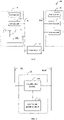
FIG. 1 is a schematic diagram of a circuit structure of a memory according to an embodiment of the present application; -
FIG. 2 is a schematic diagram of a circuit structure of a sense amplifier according to another embodiment of the present application; -
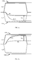
FIG. 3a, FIG. 3b , andFIG. 3c are each a schematic diagram of comparison between pull amplitudes of a voltage of a bit line and a voltage of a reference bit line according to the present application; -
FIG. 4 is a schematic diagram of a circuit structure of a sense amplifier according to another embodiment of the present application; -
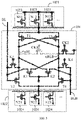
FIG. 5 is a schematic diagram of a circuit structure of a sense amplifier according to another embodiment of the present application; -
FIG. 6 is a time sequence diagram of data read according to another embodiment of the present application; and -
FIG. 7 is an equivalent circuit diagram of a sense amplifier at an offset cancellation stage according to another embodiment of the present application; and -
FIG. 8 is a schematic diagram of a procedure of a control method of a sense amplifier according to another embodiment of the present application. - In order to make the objectives, technical solutions and advantages of the present application clearer, the following clearly and completely describes the technical solutions in the present application with reference to the accompanying drawings in the present application. Apparently, the described embodiments are some rather than all of the embodiments of the present application. All other embodiments obtained by those of ordinary skill in the art based on the embodiments of the present application without creative efforts should fall within the protection scope of the present application.
- As shown in
FIG. 1 , an embodiment of the present application provides amemory 100. Thememory 100 includes asense amplifier 10 and a plurality ofmemory cells 21. A plurality ofmemory cells 21 constitute afirst storage array 20, and a plurality ofmemory cells 21 constitute asecond storage array 30. Eachmemory cell 21 in thefirst storage array 20 is connected to a bit line BL of thefirst storage array 20, and eachmemory cell 21 in thesecond storage array 30 is connected to a bit line BL of thesecond storage array 30. - The
sense amplifier 10 is located between thefirst storage array 20 and thesecond storage array 30, a first terminal of thesense amplifier 10 is connected to a first power supply terminal, a second terminal of thesense amplifier 10 is connected to a second power supply terminal, a third terminal of thesense amplifier 10 is connected to the bit line of thefirst storage array 20, and a fourth terminal of thesense amplifier 10 is connected to the bit line of thesecond storage array 30. - Each
memory cell 21 is configured to store one-bit data, the bit line of thefirst storage array 20 is configured to access data stored in eachmemory cell 21 in thefirst storage array 20, and the bit line of thesecond storage array 30 is configured to access data stored in eachmemory cell 21 in thesecond storage array 30. Thesense amplifier 10 is configured to amplify the data stored in eachmemory cell 21, and present the data on the bit line of thefirst storage array 20 and the bit line of thesecond storage array 30. Thesense amplifier 10 is further configured to: after a data read operation is completed once, restore thememory cell 21 to a state before the read operation. - Each
memory cell 21 includes a storage capacitor C and an access transistor T, a first terminal of the storage capacitor C is connected to a fixed power supply, which is, for example, 0.5 VCC , a second terminal of the storage capacitor C is connected to a first terminal of the access transistor T, a second terminal of the access transistor T is connected to the bit line, and a control terminal of the access transistor T is connected to a word line. - 1 and 0 in logic are represented by using a large and a small amount of charge stored in the storage capacitor C, or a high and low voltage difference between two ends of the storage capacitor C. The access transistor T is configured to control whether to allow or forbid to read or rewrite information stored in the storage capacitor C.
- For ease of description, when data in a
specific memory cell 21 in thefirst storage array 20 is read, the bit line of thefirst storage array 20 is referred to as a bit line BL, and the bit line of thesecond storage array 30 is referred to as a reference bit line BLB. When data in aspecific memory cell 21 in thesecond storage array 30 is read, the bit line of thesecond storage array 30 is referred to as a bit line BL, and the bit line BL of thefirst storage array 20 is referred to as a reference bit line BLB. - As a line width of the memory shrinks, a capacitance of a memory cell in the memory decreases, and a noise of a circuit in the memory seriously affects sensing resolution of the sense amplifier. Therefore, an offset cancellation sense amplifier is used in the semiconductor memory.
- In the offset cancellation sense amplifier, an amplification module includes two N-type transistors and two P-type transistors. The two P-type transistors remain cross-coupled at all times. At an idle stage and an offset cancellation stage, the two N-type transistors are connected by a diode. At another work stage, the two N-type transistors are connected in another manner.
- A process of reading data "1" from one
memory cell 21 in thefirst storage array 20 is described below. Reading data includes the idle stage, the offset cancellation stage, a precharge stage, an access stage, an amplification stage, and a restore stage. - At the idle stage, a single cross-coupled circuit is formed inside the amplification module. In other words, the two P-type transistors constitute a cross-coupled inverter, both the two N-type transistors are connected by a diode, and a charge power supply charges the bit line BL and the reference bit line BLB.
- At the offset cancellation stage, a single cross-coupled circuit continues to be formed in the amplification module. Because there is a manufacturing difference between the two transistors connected by a diode, a compensation voltage occurs on the bit line BL and the reference bit line BLB. The compensation voltage may be used to cancel the transistor manufacturing difference in the diode-connected transistor pair (which may be referred to as an offset voltage).
- At the precharge stage, a single cross-coupled circuit is constituted in the amplification module. In other words, two transistors constitute a cross-coupled inverter, and control terminals of the other two transistors are left hanging, such that the power supply pulls a voltage at a connection point between the N-type transistor and the P-type transistor, and the compensation voltage is reserved at the connection point.
- At the access stage, a double cross-coupled circuit is constituted in the amplification module. In other words, the two P-type transistors constitute a cross-coupled inverter, and the two N-type transistors also constitute a cross-coupled inverter, such that a connection point between the N-type transistor and the P-type transistor pulls voltages of the bit line and the reference bit line to a reference voltage, and the compensation voltage is reserved on the bit line BL and the reference bit line BLB. A signal on a word line corresponding to the accessed
memory cell 21 is controlled, such that an access transistor T in the accessedmemory cell 21 is on, the storage capacitor C enables the voltage of the bit line BL to rise, and the voltage of the bit line BL is higher than the reference voltage. - At the amplification stage, the voltage of the bit line BL is higher than the reference voltage, such that the
sense amplifier 10 pulls up the voltage of the bit line BL, and the sense amplifier pulls down the voltage of the reference bit line BLB. Because the compensation voltage is reserved on the bit line BL and the reference bit line BLB, the transistor manufacturing difference in the transistor pair can be canceled at the amplification stage, such that a voltage difference between the bit line BL and the reference bit line BLB can reflect that data in the accessedmemory cell 21 is "1". - At the restore stage, the
sense amplifier 10 stabilizes the voltages of the bit line BL and the reference bit line BLB at logical data "1", the bit line BL further charges the storage capacitor C, and after a specific time of charging, charge in the storage capacitor C is restored to a state before the read operation. Then, a signal inside a line is selected by a control column, such that an external read circuit can read the data stored in the accessedmemory cell 21 on the bit line BL and the reference bit line BLB. - However, after the offset cancellation stage, the precharge stage, and the amplification stage, the external read circuit is prone to incorrectly reading data presented on the bit line BL and the reference bit line BLB.
- To resolve the foregoing problem, the present application provides a sense amplifier, a memory, and a control method. A technical concept of the present application is that when being at an offset cancellation stage, the sense amplifier controls a controlled power module to supply power to an amplification module, and the amplification module controls a value of a compensation voltage on a bit line BL and a reference bit line BLB at an offset cancellation stage, to enable the compensation voltage to be within a rated voltage range, so as to ensure that an external read circuit can accurately read data on the bit line BL and the reference bit line BLB at a restore stage.
- As shown in
FIG. 2 , an embodiment of the present application provides asense amplifier 10, thesense amplifier 10 includes anamplification module 101 and a controlledpower module 102, and theamplification module 101 is connected to the controlledpower module 102. - The
amplification module 101 is configured to amplify a voltage difference between a bit line BL and a reference bit line BLB when thesense amplifier 10 is at an amplification stage. The controlledpower module 102 is configured to determine a drive parameter according to a rated compensation voltage range between the bit line BL and the reference bit line BLB, and supply power to theamplification module 101 according to the drive parameter. - Under control of the controlled
power module 102, theamplification module 101 pulls a compensation voltage (which may also be referred to as an offset voltage) between the bit line BL and the reference bit line BLB to be a rated compensation voltage at an offset cancellation stage. The rated compensation voltage is within the rated compensation voltage range. The compensation voltage refers to a voltage difference between a voltage of the bit line and a voltage of the reference bit line at the offset cancellation stage. For example, the voltage on the bit line BL minus the voltage on the reference bit line BLB equals the compensation voltage, or the voltage on the reference bit line BLB minus the voltage on the bit line BL equals the compensation voltage. - In a process of reading data in a memory cell, a value of the compensation voltage on the bit line BL and the reference bit line BLB affects data read accuracy. If the compensation voltage on the bit line BL and the reference bit line BLB is excessively large, the compensation voltage is used as an interference factor. Consequently, logical data in the memory cell cannot be accurately presented on the bit line BL and the reference bit line BLB. If the compensation voltage is excessively small, an offset caused by an element manufacturing difference cannot be compensated, and the element manufacturing difference still causes a voltage offset on the bit line BL and the reference bit line BLB. Consequently, logical data in the memory cell cannot be accurately presented on the bit line BL and the reference bit line BLB.
- A driving capability of the controlled
power module 102 affects a value of the compensation voltage on the bit line BL and the reference bit line BLB at the offset cancellation stage. As shown inFIG. 3a and FIG. 3b , if a first terminal vp (t) and a second terminal vn (t) of the sense amplifier has an excessively strong voltage pulling capability, a value of the compensation voltage Vos on the bit line BL and the reference bit line BLB may be excessively large. Consequently, an external read circuit always reads logical data "1" or logical "0" when reading data on the bit line BL and the reference bit line BLB. - As shown in
FIG. 3c , in this embodiment, at a sense amplifier design stage, the rated compensation voltage range may be obtained by simulation, and at a sense amplifier manufacturing stage, the rated compensation voltage range may be obtained by a test. The drive parameter is determined according to the rated compensation voltage range between the bit line BL and the reference bit line BLB, and power is supplied to theamplification module 101 according to the drive parameter. Under control of the controlledpower module 102, theamplification module 101 pulls the compensation voltage Vos between the bit line BL and the reference bit line BLB to the rated compensation voltage at the offset cancellation stage. - The rated compensation voltage is within the rated compensation voltage range. After a precharge stage, an access stage, and the amplification stage, the voltage offset that is on the bit line BL and the reference bit line BLB and that is caused by the element manufacturing difference is canceled or partially offset by the rated compensation voltage, and the compensation voltage is not introduced as an interference factor, such that logical data in the memory cell can be accurately presented on the bit line BL and the reference bit line BLB.
- In the foregoing technical solution, the controlled power module determines the drive parameter according to the rated compensation voltage range, and supplies power to the amplification module according to the drive parameter, to control the amplification module to pull the compensation voltage between the bit line BL and the reference bit line BLB to the rated compensation voltage at the offset cancellation stage. Therefore, the voltage offset that is on the bit line BL and the reference bit line BLB and that is caused by the element manufacturing difference is canceled or partially offset by the rated compensation voltage, and the compensation voltage is not introduced as an interference factor, such that logical data in the memory cell can be accurately presented on the bit line BL and the reference bit line BLB, and the external read circuit can accurately read the data on the bit line BL and the reference bit line BLB.
- As shown in
FIG. 4 , an embodiment of the present application provides asense amplifier 10, thesense amplifier 10 includes anamplification module 101 and a controlledpower module 102, and theamplification module 101 is connected to the controlledpower module 102. - The controlled
power module 102 includes a first controlledpower unit 1021, a second controlledpower unit 1022, and acontrol unit 1025. Theamplification module 101 is provided with a first terminal, a second terminal, a third terminal, and a fourth terminal. - An output terminal of the first controlled
power unit 1021 is connected to the first terminal of theamplification module 101, an output terminal of the second controlledpower unit 1022 is connected to the second terminal of theamplification module 101, thecontrol unit 1025 is connected to a control terminal of the first controlledpower unit 1021, and thecontrol unit 1025 is further connected to a control terminal of the second controlledpower unit 1022. - Both the first controlled
power unit 1021 and the second controlledpower unit 1022 are configured to supply power to theamplification module 101, and thecontrol unit 1025 is configured to: determine a drive parameter according to a rated compensation voltage range between a bit line BL and a reference bit line BLB, and control, according to the drive parameter, a first controlledcurrent source 1023 and a second controlledcurrent source 1024 to supply power to theamplification module 101. - Under control of the first controlled
power unit 1021 and the second controlledpower unit 1022, the amplification module pulls a compensation voltage between the bit line BL and the reference bit line BLB to a rated compensation voltage at an offset cancellation stage. The rated compensation voltage is within the rated compensation voltage range. - The drive parameter is determined according to the rated compensation voltage range between the bit line BL and the reference bit line BLB, and power is supplied to the amplification module according to the drive parameter. Under control of the controlled power module, the amplification module pulls the compensation voltage between the bit line BL and the reference bit line BLB to the rated compensation voltage at the offset cancellation stage.
- The rated compensation voltage is within the rated compensation voltage range. After the offset cancellation stage, a precharge stage, an access stage, and an amplification stage, a voltage offset that is on the bit line BL and the reference bit line BLB and that is caused by an element manufacturing difference is canceled or partially offset by the rated compensation voltage, and the compensation voltage is not introduced as an interference factor, such that logical data in a memory cell can be accurately presented on the bit line BL and the reference bit line BLB.
- In another embodiment, the first controlled
power unit 1021 includes N first controlledcurrent sources 1023. Each first controlledcurrent source 1023 is provided with a control terminal, a first terminal, and a second terminal. The second terminal of each first controlledcurrent source 1023 is the output terminal of the first controlledpower unit 1021, and the control terminal of each first controlledcurrent source 1023 is the control terminal of the first controlledpower unit 1021. The first terminal of the first controlledcurrent source 1023 is connected to a first power supply terminal, and the second terminal of the first controlledcurrent source 1023 is connected to the first terminal of theamplification module 101. The control terminal of the first controlledcurrent source 1023 is connected to thecontrol unit 1025, where N is a positive integer. - The second controlled
power unit 1022 includes N second controlledcurrent sources 1024, and each second controlledcurrent source 1024 is provided with a control terminal, a first terminal, and a second terminal. The second terminal of each second controlledcurrent source 1024 is the output terminal of the second controlledpower unit 1022, and the control terminal of each second controlledcurrent source 1024 is the control terminal of the second controlledpower unit 1022. The first terminal of the second controlledcurrent source 1024 is connected to a second power supply terminal, and the second terminal of the second controlledcurrent source 1024 is connected to the second terminal of theamplification module 101. The control terminal of the second controlledcurrent source 1024 is connected to thecontrol unit 1025. - The control unit is configured to: determine a first drive current range and a second drive current range according to the rated compensation voltage range, select at least one first target current source in the N first controlled current sources, and select at least one second target current source in the N second controlled current sources. A total current provided by the at least one first target current source is within the first drive current range, and a total current provided by the at least one second target current source is within the second drive current range. The control unit further generates a first control signal used to control the first target current source to work, and generates a second control signal used to control the second target current source to work, to enable the first controlled power unit to control the amplification module to pull voltages of the bit line BL and the reference bit line BLB at the offset cancellation stage, and enable the second controlled power unit to control the amplification module to pull voltages of the bit line BL and the reference bit line BLB at the offset cancellation stage, to further pull the compensation voltage between the bit line BL and the reference bit line BLB to be the rated compensation voltage at the offset cancellation stage.
- In another embodiment, an i th first controlled
current source 1023 provides a drive current 2 i-1 × Ib , a j th second controlledcurrent source 1024 provides a drive current 2 j-1 × Ib , and Ib represents a unit current. The N first controlledcurrent sources 1023 may provide 2 N - 1 levels of drive current, and the N second controlledcurrent sources 1024 may also provide 2 N - 1 levels of drive current. Rates at which theamplification module 101 pulls the voltage of the bit line and the voltage of the reference bit line can be accurately adjusted by adjusting an amplitude value of the unit current, to further control amplitude values for pulling the voltage of the bit line and the voltage of the reference bit line, so as to accurately control the compensation voltage between the bit line BL and the reference bit line BLB to be within the rated compensation voltage range at the offset cancellation stage. - In the foregoing embodiment, work states of the first controlled current source and the second controlled current source are controlled, to control a drive parameter of the first controlled power unit and the second controlled power unit, and control rates at which the amplification module pulls the voltages of the bit line BL and the reference bit line, to further control amplitudes for pulling the voltage of the bit line and the voltage of the reference bit line, and control the amplification module to pull the compensation voltage between the bit line BL and the reference bit line BLB to be the rated compensation voltage at the offset cancellation stage. In this case, the voltage offset that is on the bit line BL and the reference bit line BLB and that is caused by the element manufacturing difference is canceled or partially offset by the rated compensation voltage, and the compensation voltage is not introduced as an interference factor, such that logical data in the memory cell can be accurately presented on the bit line BL and the reference bit line BLB, and the external read circuit can accurately read the data on the bit line BL and the reference bit line BLB.
- As shown in
FIG. 5 , an embodiment of the present application provides asense amplifier 10, thesense amplifier 10 includes anamplification module 101 and a controlledpower module 102, and theamplification module 101 is connected to the controlledpower module 102. - The
amplification module 101 includes at least one cross-coupled amplifier circuit, each cross-coupled amplifier circuit is provided with a first terminal, a second terminal, a third terminal, and a fourth terminal, the first terminal of the cross-coupled amplifier circuit is connected to an output terminal of a first controlledpower unit 1021, the second terminal of the cross-coupled amplifier circuit is connected to an output terminal of the second controlledpower unit 1022, the third terminal of the cross-coupled amplifier circuit is connected to a bit line BL, and the fourth terminal of the cross-coupled amplifier circuit is connected to a reference bit line BLB. - The cross-coupled amplifier circuit is a single cross-coupled amplifier circuit and has an offset cancellation function, and the cross-coupled circuit specifically includes: a first transistor T1, a second transistor T2, a third transistor T3, a fourth transistor T4, a first switch K1, a second switch K2, a third switch K3, and a fourth switch K4.
- A first terminal of the first transistor T1 is the first terminal of the cross-coupled amplifier circuit, a second terminal of the second transistor T2 is the second terminal of the cross-coupled amplifier circuit, a second terminal of the first transistor T1 is the third terminal of the cross-coupled amplifier circuit, and a second terminal of the third transistor T3 is the fourth terminal of the cross-coupled amplifier circuit.
- The second terminal of the first transistor T1 is connected to a first terminal of the second transistor T2, the second terminal of the third transistor T3 is connected to a first terminal of the fourth transistor T4, the first terminal of the first transistor T1 is connected to a first terminal of the third transistor T3, and the second terminal of the second transistor T2 is connected to a second terminal of the fourth transistor T4.
- A control terminal of the first transistor T1 is connected to the second terminal of the third transistor T3, a control terminal of the second transistor T2 is connected to the second terminal of the third transistor T3 by the first switch K1, and the control terminal of the second transistor T2 is connected to the first terminal of the second transistor T2 by the third switch K3.
- A control terminal of the third transistor T3 is connected to the second terminal of the first transistor T1, a control terminal of the fourth transistor T4 is connected to the second terminal of the first transistor T1 by the second switch K2, and the control terminal of the fourth transistor T4 is connected to the first terminal of the fourth transistor T4 by the fourth switch K4.
- The first transistor T1 and the third transistor T3 are P-type transistors, and the second transistor T2 and the fourth transistor T4 are N-type transistors.
- The controlled
power module 102 includes the first controlledpower unit 1021 and the second controlledpower unit 1022, the first controlledpower unit 1021 includes N first controlledcurrent sources 1023, and the second controlledpower unit 1022 includes N second controlledcurrent sources 1024. The first controlledcurrent source 1023 is a P-type transistor, and the second controlledcurrent source 1024 is an N-type transistor. - A process of reading data "1" from one
memory cell 21 in thefirst storage array 20 is described below. For ease of description, a connection line between the second terminal of the first transistor T1 and the first terminal of the second transistor T2 is referred to as an internal bit line nBL of afirst storage array 20, and a connection line between the second terminal of the third transistor T3 and the first terminal of the fourth transistor T4 is referred to as an internal reference bit line nBLB of thefirst storage array 20. - As shown in
FIG. 6 , reading data includes an idle stage, an offset cancellation stage, a precharge stage, an access stage, an amplification stage, and a restore stage. - At the idle stage, the first switch K1 to the fourth switch K4 are closed. The control terminal of the second transistor T2 is connected to the second terminal of the third transistor T3, the control terminal of the second transistor T2 is connected to the first terminal of the second transistor T2, the control terminal of the fourth transistor T4 is connected to the second terminal of the first transistor T1, and the control terminal of the fourth transistor T4 is connected to the first terminal of the fourth transistor T4. The charge switches CK1 and CK2 are closed, and the internal bit line nBL and the internal reference bit line nBLB are charged by a charge power supply. In this case, in an embodiment, the bit line BL, the reference bit line BLB, the internal bit line nBL, and the internal reference bit line nBLB are all charged to 0.5 VCC .
- At the offset cancellation stage, the first switch K1 and the second switch K2 are disconnected, and the third switch K3 and the fourth switch K4 are still closed. As shown in
FIG. 7 , the first terminal of the second transistor T2 is connected to the control terminal of the second transistor T2, the first terminal of the fourth transistor T4 is connected to the control terminal of the fourth transistor T4, both the two N-type transistors are connected by a diode, and the two P-type transistors constitute a cross-coupled inverter. Because there is a manufacturing difference between the two transistors connected by a diode, a compensation voltage occurs on the bit line BL and the reference bit line BLB. The compensation voltage may be used to cancel the transistor manufacturing difference in the N-type transistor pair. At least one N-type transistor of N11, N12, N13 is controlled according to a waveform in the figure, and at least one N-type transistor of N21, N22, N23 is controlled according to a waveform in the figure, to control a drive parameter of the first controlledpower unit 1021 and the second controlledpower unit 1022, so as to control amplitude values for pulling voltages of the bit line BL and the reference bit line by the cross-coupled amplifier circuit at the offset cancellation stage, such that the compensation voltage between the bit line BL and the reference bit line BLB is pulled to be the rated compensation voltage. - At the precharge stage, the first switch K1 to the fourth switch K4 are all disconnected. In other words, the two N-type transistors constitute a cross-coupled inverter, and control terminals of the other two transistors are left hanging. Both a voltage of the internal bit line nBL of the
first storage array 20 and a voltage of the internal reference bit line nBLB are pulled up to a reference voltage, and the reference voltage is a voltage of a fixed power supply connected to the storage capacitor C. In an embodiment, the voltage of the fixed power supply is 0.5 VCC . - At the access stage, the first switch K1 and the second switch K2 are closed, and the third switch K3 and the fourth switch K4 continue to be disconnected. A double cross-coupled circuit is constituted in the amplification module. In other words, two transistors constitute a cross-coupled inverter, and the other two transistors also constitute a cross-coupled inverter. The internal bit line nBL pulls the voltage of the bit line, the internal reference bit line nBLB pulls the voltage of the reference bit line, and the compensation voltage is still reserved on the bit line BL and the reference bit line BLB. For example, at the offset cancellation stage, the voltage on the bit line BL is higher than the voltage of the reference bit line BLB, and a difference is a compensation voltage Vos. At the access stage, the voltage on the bit line BL is still higher than the voltage of the reference bit line BLB, and a difference is also the compensation voltage Vos. If an offset between threshold voltages of T2 and T4 is Vos, an offset between threshold voltages of T5 and T7 is Vos, or an offset between threshold voltages that occur on T6 and T5 together with T8 and T7 is Vos, at the access stage, impact of Vos on the sense amplifier is eliminated or at least weakened.
- A signal on a word line corresponding to the accessed
memory cell 21 is controlled, such that an access transistor T in the accessedmemory cell 21 is on, the storage capacitor C enables the voltage of the bit line BL to rise, and the voltage of the bit line is higher than the reference voltage. - At the amplification stage, the first switch K1 and the second switch K2 continue to be closed, and the third switch K3 and the fourth switch K4 continue to be disconnected. At least one P-type transistor of N11, N12, N13 is controlled according to a waveform in the figure, and at least one N-type transistor of N21, N22, N23 is controlled according to a waveform in the figure, to control a drive parameter of the first controlled
power unit 1021 and the second controlledpower unit 1022, so as to control amplitude values for pulling voltages of the bit line BL and the reference bit line by the cross-coupled amplifier circuit at the amplification stage. The voltage of the bit line BL is higher than the reference voltage, such that thesense amplifier 10 pulls up the voltage of the bit line BL, and the sense amplifier pulls down the voltage of the reference bit line BLB. Because the compensation voltage is reserved on the bit line BL and the reference bit line BLB, the manufacturing difference between the N-type transistors in the sense amplifier can be offset or canceled at the amplification stage, such that a voltage difference between the bit line BL and the reference bit line BLB can reflect that data in the accessedmemory cell 21 is "1". - At the restore stage, the
sense amplifier 10 stabilizes the voltages of the bit line BL and the reference bit line BLB at logical data "1", the bit line BL further charges the storage capacitor C, and after a specific time of charging, charge in the storage capacitor C is restored to a state before the read operation. Then, a signal inside a line is selected by a control column, such that an external read circuit can read the data stored in the accessedmemory cell 21 on the bit line BL and the reference bit line BLB. - In another embodiment, an i th P-type transistor in the first controlled
power unit 1021 may provide a drive current 2 i-1 × Ib , a j th N-type transistor in the second controlledpower unit 1022 may provide a drive current 2 j-1 × Ib , and Ib represents a unit current. The first controlledpower unit 1021 may provide 2 N - 1 levels of drive current, and the second controlledpower unit 1022 may also provide 2 N - 1 levels of drive current, such that (2 N - 1)(2 N - 1) levels of compensation voltage can be obtained. - A level of a drive current that may be provided by the controlled
power module 102 is described by using an example below. The first controlledpower unit 1021 includes three P-type transistors. A drive current that may be provided by the 1st P-type transistor is Ib , a drive current that may be provided by the 2nd P-type transistor is 2Ib , and a drive current that may be provided by the 3rd P-type transistor is 4Ib .The second controlledpower unit 1022 includes three N-type transistors. A drive current that may be provided by the 1st N-type transistor is Ib , a drive current that may be provided by the 2nd N-type transistor is 2Ib , and a drive current that may be provided by the 3rd N-type transistor is 4Ib . - The controlled
power module 102 may provide 7 levels of drive current. Control signals of N-type transistors and P-type transistors at each level are shown in Table 1 and Table 2. "1" represents a high level control signal and "0" represents a low level control signal.Table 1 Control signal of an N-type transistor 3rd N-type transistor 2nd N-type transistor 1st N-type transistor Level of a drive current 0 0 1 Ib 0 1 0 2Ib 0 1 1 3Ib 1 0 0 4Ib 1 0 1 5Ib 1 1 0 6Ib 1 1 1 7Ib Table 2 Control signal of a P-type transistor 3rd P-type transistor 2nd P-type transistor 1st P-type transistor Level of a drive current 1 1 0 Ib 1 0 1 2Ib 1 0 0 3Ib 0 1 1 4Ib 0 1 0 5Ib 0 0 1 6Ib 0 0 0 7Ib - In the technical solution, an on state of the P-type transistor and an on state of the N-type transistor are controlled, to control the controlled power module to provide the level of the drive current to the amplification module, so as to control amplitude values for pulling the voltage of the bit line and the voltage of the reference bit line by the amplification module at the offset cancellation stage, and the amplification module may be controlled to pull the compensation voltage between the bit line BL and the reference bit line BLB to be the rated compensation voltage at the offset cancellation stage. Therefore, the voltage offset that is on the bit line BL and the reference bit line BLB and that is caused by the element manufacturing difference is canceled or partially offset by the rated compensation voltage, and the compensation voltage is not introduced as an interference factor, such that logical data in the memory cell can be accurately presented on the bit line BL and the reference bit line BLB, and the external read circuit can accurately read the data on the bit line BL and the reference bit line BLB.
- As shown in
FIG. 8 , an embodiment of the present application provides a control method of a sense amplifier. A structure of the sense amplifier has been described in detail in the foregoing embodiment, and details are not described herein again. The control method specifically includes the following steps. - S1001. Obtain a rated compensation voltage range between a bit line and a reference bit line.
- At a sense amplifier design stage, the rated compensation voltage range may be obtained by simulation, and at a sense amplifier manufacturing stage, the rated compensation voltage range may be obtained by a test. When a compensation voltage between a bit line and a reference bit line is within the rated compensation voltage range, data on the bit line and the reference bit line can be accurately read. In other words, a voltage offset that is on the bit line and the reference bit line and that is caused by an element manufacturing difference is canceled or partially offset by the rated compensation voltage, and the compensation voltage is not introduced as an interference factor, such that logical data in a memory cell can be accurately presented on the bit line and the reference bit line, and an external read circuit can accurately read the data on the bit line and the reference bit line.
- S1002. Determine a drive parameter according to the rated compensation voltage range.
- The sense amplifier is tested, to obtain a mapping relationship between the compensation voltage between the bit line and the reference bit line and a drive parameter of a controlled power module, and then determine the drive parameter of the controlled power module according to the mapping relationship and the rated compensation voltage range.
- S1003. Generate, according to the drive parameter, a control signal used to control the amplification module.
- After the drive parameter of the controlled power module is obtained, the control signal is generated according to the drive parameter, to control the controlled power module to supply power to the amplification module according to the drive parameter, and further control the amplification module to pull the compensation voltage between the bit line or the reference bit line to the rated compensation voltage at the offset cancellation stage. The rated compensation voltage is within the rated compensation voltage range.
- In the foregoing technical solution, the controlled power module determines the drive parameter according to the rated compensation voltage range, and supplies power to the amplification module according to the drive parameter, to control the amplification module to pull the compensation voltage between the bit line and the reference bit line to the rated compensation voltage at the offset cancellation stage. Therefore, the voltage offset that is on the bit line and the reference bit line and that is caused by the element manufacturing difference is canceled or partially offset by the rated compensation voltage, and the compensation voltage is not introduced as an interference factor, such that logical data in the memory cell can be accurately presented on the bit line and the reference bit line, and the external read circuit can accurately read the data on the bit line and the reference bit line.
- The present application further provides a control method of a sense amplifier. A structure of the sense amplifier has been described in detail in the foregoing embodiment, and details are not described herein again. The control method specifically includes the following steps.
- S2001. Obtain a rated compensation voltage range between a bit line and a reference bit line.
- The step has been described in detail in the foregoing embodiment, and details are not described herein again.
- S2002. Determine a first drive current range and a second drive current range according to the rated compensation voltage range.
- The sense amplifier is tested, to obtain a mapping relationship between a compensation voltage between the bit line and the reference bit line and a drive current of a first controlled power unit and a second controlled power unit, and then determine the first drive current range of the first controlled power module and the second drive current range of the second controlled power module according to the mapping relationship and the rated compensation voltage range.
- S2003. Generate, according to the drive parameter, a control signal used to control the amplification module.
- After the first drive current range is determined, at least one first target current source is selected in N first controlled current sources, to ensure that a total current provided by the at least one first target current source is within the first drive current range. In addition, after the second drive current range is determined, at least one second target current source is selected in N second controlled current sources, to ensure that a total current provided by the at least one second target current source is within the second drive current range. Then, a first control signal used to control the first target current source to work is generated, and a second control signal used to control the second target current source to work is generated. The first controlled power unit and the second controlled power unit control the amplification module to pull the compensation voltage between the bit line and the reference bit line to be a rated compensation voltage at an offset cancellation stage. The rated compensation voltage is within the rated compensation voltage range.
- In the foregoing embodiment, work states of the first controlled current source and the second controlled current source are controlled, to control the controlled power module to provide a level of a drive current to the amplification module, so as to control amplitude values for pulling a voltage of the bit line and a voltage of the reference bit line by the amplification module at the offset cancellation stage, and the amplification module may be controlled to pull the compensation voltage between the bit line and the reference bit line to be the rated compensation voltage at the offset cancellation stage. Therefore, a voltage offset that is on the bit line and the reference bit line and that is caused by an element manufacturing difference is canceled or partially canceled by the rated compensation voltage, and the compensation voltage is not introduced as an interference factor, such that logical data in a memory cell can be accurately presented on the bit line and the reference bit line, and an external read circuit can accurately read the data on the bit line and the reference bit line.
- Finally, it should be noted that the above embodiments are merely used to explain the technical solutions of the present application, but are not intended to limit the present application. Although the present application is described in detail with reference to the foregoing embodiments, those of ordinary skill in the art should understand that they can still modify the technical solutions described in the foregoing embodiments, or make equivalent substitutions on some or all technical features therein. These modifications or substitutions do not make the essence of the corresponding technical solutions deviate from the technical solutions of the embodiments of the present application.
Claims (14)
- A sense amplifier, comprising:an amplification module, configured to: when the sense amplifier is at an amplification stage, amplify a voltage difference between a bit line and a reference bit line; anda controlled power module, connected to the amplification module, and configured to: determine a drive parameter according to a rated compensation voltage range between the bit line and the reference bit line, and supply power to the amplification module according to the drive parameter, so as to control the amplification module to pull a compensation voltage between the bit line and the reference bit line to be a rated compensation voltage at an offset cancellation stage; wherein the rated compensation voltage is within the rated compensation voltage range.
- The sense amplifier according to claim 1, wherein the controlled power module comprises:a first controlled power unit, connected to a first terminal of the amplification module, and configured to supply power to the amplification module;a second controlled power unit, connected to a second terminal of the amplification module, and configured to supply power to the amplification module; anda control unit, connected to the first controlled power unit, further connected to the second controlled power unit, and configured to: determine the drive parameter according to the rated compensation voltage range, and control the first controlled power unit and the second controlled power unit to supply power to the amplification module according to the drive parameter.
- The sense amplifier according to claim 2, wherein the first controlled power unit comprises:
N first controlled current sources, wherein the first controlled current source is provided with a control terminal, a first terminal, and a second terminal; the first terminal of the first controlled current source is connected to a first power supply terminal, the second terminal of the first controlled current source is connected to the first terminal of the amplification module, the control terminal of the first controlled current source is connected to the control unit, and N is a positive integer. - The sense amplifier according to claim 3, wherein the second controlled power unit comprises:
N second controlled current sources, wherein the second controlled current source is provided with a control terminal, a first terminal, and a second terminal; the first terminal of the second controlled current source is connected to a second power supply terminal, the second terminal of the second controlled current source is connected to the second terminal of the amplification module, and the control terminal of the second controlled current source is connected to the control unit. - The sense amplifier according to claim 4, wherein the control unit is configured to:determine a first drive current range and a second drive current range according to the rated compensation voltage range;select at least one first target current source in the N first controlled current sources, and select at least one second target current source in the N second controlled current sources; wherein a total current provided by the at least one first target current source is within the first drive current range, and a total current provided by the at least one second target current source is within the second drive current range; andgenerate a first control signal used to control the first target current source to work, and generate a second control signal used to control the second target current source to work; such that the first controlled power unit controls the amplification module to pull voltages of the bit line and the reference bit line at the offset cancellation stage, and the second controlled power unit controls the amplification module to pull voltages of the bit line and the reference bit line at the offset cancellation stage.
- The sense amplifier according to any one of claims 3 to 5, wherein a drive current of an i th first current source is 2 i-1 × Ib , a drive current of a j th second current source is 2 j-1 × Ib , and Ib represents a unit current.
- The sense amplifier according to any one of claims 4 to 5, wherein the first controlled current source is a P-type transistor, and the second controlled current source is an N-type transistor.
- The sense amplifier according to any one of claims 2 to 5, wherein the amplification module comprises:
at least one cross-coupled amplifier circuit, wherein the cross-coupled amplifier circuit is provided with a first terminal, a second terminal, a third terminal, and a fourth terminal; the first terminal of the cross-coupled amplifier circuit is connected to an output terminal of the first controlled power unit, the second terminal of the cross-coupled amplifier circuit is connected to an output terminal of the second controlled power unit, the third terminal of the cross-coupled amplifier circuit is connected to the bit line, and the fourth terminal of the cross-coupled amplifier circuit is connected to the reference bit line. - The sense amplifier according to claim 8, wherein the cross-coupled amplifier circuit comprises: a first transistor, a second transistor, a third transistor, a fourth transistor, a first switch, a second switch, a third switch, and a fourth switch;a first terminal of the first transistor is the first terminal of the cross-coupled amplifier circuit, a second terminal of the second transistor is the second terminal of the cross-coupled amplifier circuit, a second terminal of the first transistor is the third terminal of the cross-coupled amplifier circuit, and a second terminal of the third transistor is the fourth terminal of the cross-coupled amplifier circuit;the second terminal of the first transistor is connected to a first terminal of the second transistor, the second terminal of the third transistor is connected to a first terminal of the fourth transistor, the first terminal of the first transistor is connected to a first terminal of the third transistor, and the second terminal of the second transistor is connected to a second terminal of the fourth transistor;a control terminal of the first transistor is connected to the second terminal of the third transistor, a control terminal of the second transistor is connected to the second terminal of the third transistor by the first switch, and the control terminal of the second transistor is connected to the first terminal of the second transistor by the third switch; anda control terminal of the third transistor is connected to the second terminal of the first transistor, a control terminal of the fourth transistor is connected to the second terminal of the first transistor by the second switch, and the control terminal of the fourth transistor is connected to the first terminal of the fourth transistor by the fourth switch.
- The sense amplifier according to claim 9, wherein the first transistor and the third transistor are P-type transistors, and the second transistor and the fourth transistor are N-type transistors.
- A memory, comprising the sense amplifier according to any one of claims 1 to 10 and a memory cell, wherein
a plurality of memory cells constitute a first storage array, a plurality of memory cells constitute a second storage array, the sense amplifier is located between the first storage array and the second storage array, a third terminal of the sense amplifier is connected to a bit line of the first storage array, and a fourth terminal of the sense amplifier is connected to a reference bit line of the second storage array. - A control method of a sense amplifier, wherein the sense amplifier comprises an amplification module and a controlled power module; and the control method comprises:obtaining a rated compensation voltage range between a bit line and a reference bit line;determining a drive parameter according to the rated compensation voltage range; andgenerating, according to the drive parameter, a control signal used to control the amplification module, so as to control the amplification module to pull a compensation voltage between the bit line and the reference bit line to be a rated compensation voltage at an offset cancellation stage; wherein the rated compensation voltage is within the rated compensation voltage range.
- The control method of a sense amplifier according to claim 12, wherein the determining a drive parameter according to the rated compensation voltage range comprises:
determining a first drive current range and a second drive current range according to the rated compensation voltage range. - The control method of a sense amplifier according to claim 13, wherein the controlled power module comprises a first controlled power unit and a second controlled power unit;
and the generating, according to the drive parameter, a control signal used to control the amplification module comprises:selecting at least one first target current source in N first controlled current sources, and selecting at least one second target current source in N second controlled current sources, wherein a total current provided by the at least one first target current source is within the first drive current range, and a total current provided by the at least one second target current source is within the second drive current range; andgenerating a first control signal used to control the first target current source to work, and generating a second control signal used to control the second target current source to work.
Applications Claiming Priority (2)
| Application Number | Priority Date | Filing Date | Title |
|---|---|---|---|
| CN202110313695.9A CN112992200B (en) | 2021-03-24 | 2021-03-24 | Sense amplifier, memory and control method |
| PCT/CN2021/107522 WO2022198856A1 (en) | 2021-03-24 | 2021-07-21 | Sense amplifier, memory and control method |
Publications (2)
| Publication Number | Publication Date |
|---|---|
| EP4089677A1 true EP4089677A1 (en) | 2022-11-16 |
| EP4089677A4 EP4089677A4 (en) | 2023-08-09 |
Family
ID=76334485
Family Applications (1)
| Application Number | Title | Priority Date | Filing Date |
|---|---|---|---|
| EP21904625.7A Pending EP4089677A4 (en) | 2021-03-24 | 2021-07-21 | DETECTION AMPLIFIER, MEMORY AND CONTROL METHOD |
Country Status (6)
| Country | Link |
|---|---|
| US (1) | US12112825B2 (en) |
| EP (1) | EP4089677A4 (en) |
| JP (1) | JP7383164B2 (en) |
| KR (1) | KR20220133898A (en) |
| CN (1) | CN112992200B (en) |
| WO (1) | WO2022198856A1 (en) |
Families Citing this family (16)
| Publication number | Priority date | Publication date | Assignee | Title |
|---|---|---|---|---|
| CN113284537B (en) * | 2020-01-31 | 2025-01-07 | 台湾积体电路制造股份有限公司 | Hybrid self-tracking reference circuit for RRAM cells |
| US11205495B1 (en) * | 2020-08-07 | 2021-12-21 | Micron Technology, Inc. | Read disturb mitigation based on signal and noise characteristics of memory cells collected for read calibration |
| JP7301237B2 (en) | 2021-03-24 | 2023-06-30 | チャンシン メモリー テクノロジーズ インコーポレイテッド | SENSE AMPLIFIER, MEMORY AND CONTROL METHOD |
| US11894101B2 (en) | 2021-03-24 | 2024-02-06 | Changxin Memory Technologies, Inc. | Sense amplifier, memory and control method |
| CN112992202B (en) | 2021-03-24 | 2022-08-05 | 长鑫存储技术有限公司 | Sense amplifier, memory and control method |
| CN112992200B (en) | 2021-03-24 | 2022-05-17 | 长鑫存储技术有限公司 | Sense amplifier, memory and control method |
| US11823763B2 (en) | 2021-03-24 | 2023-11-21 | Changxin Memory Technologies, Inc. | Sense amplifier, memory and control method |
| CN113517016B (en) * | 2021-07-21 | 2023-04-18 | 清华大学 | Computing device and robustness processing method thereof |
| EP4243021B1 (en) | 2021-08-27 | 2025-11-26 | Changxin Memory Technologies, Inc. | Sense amplification circuit and data readout method |
| CN115910149B (en) * | 2021-08-27 | 2025-09-05 | 长鑫存储技术有限公司 | Sense amplifier circuit and data readout method |
| CN115148238A (en) * | 2022-06-30 | 2022-10-04 | 长鑫存储技术有限公司 | Sense amplifier and semiconductor memory |
| JP7515653B1 (en) * | 2023-04-07 | 2024-07-12 | 華邦電子股▲ふん▼有限公司 | Semiconductor memory device and control method thereof |
| US20250279133A2 (en) * | 2023-06-02 | 2025-09-04 | Micron Technology, Inc. | Interface techniques for stacked memory architectures |
| US20250069655A1 (en) * | 2023-08-25 | 2025-02-27 | Tetramem Inc. | Bit-serial input schemes for crossbar circuits |
| WO2025213452A1 (en) * | 2024-04-12 | 2025-10-16 | Yangtze Memory Technologies Co., Ltd. | Memory device and operation methods thereof |
| JP7679528B1 (en) * | 2024-06-12 | 2025-05-19 | 華邦電子股▲ふん▼有限公司 | Semiconductor memory device and control method thereof |
Family Cites Families (50)
| Publication number | Priority date | Publication date | Assignee | Title |
|---|---|---|---|---|
| JPS58102389A (en) | 1981-12-12 | 1983-06-17 | Nippon Telegr & Teleph Corp <Ntt> | Storage circuit |
| US5297097A (en) | 1988-06-17 | 1994-03-22 | Hitachi Ltd. | Large scale integrated circuit for low voltage operation |
| JPH0757465A (en) | 1993-08-06 | 1995-03-03 | Mitsubishi Electric Corp | Semiconductor circuit device |
| KR960009956B1 (en) * | 1994-02-16 | 1996-07-25 | 현대전자산업 주식회사 | Sense Amplifiers in Semiconductor Devices |
| US5877993A (en) | 1997-05-13 | 1999-03-02 | Micron Technology, Inc. | Memory circuit voltage regulator |
| JP3913377B2 (en) | 1998-11-04 | 2007-05-09 | 富士通株式会社 | Semiconductor memory device |
| JP2002025268A (en) * | 2000-07-13 | 2002-01-25 | Seiko Epson Corp | Semiconductor device |
| DE10112281B4 (en) | 2001-03-14 | 2006-06-29 | Infineon Technologies Ag | Sense amplifier arrangements for a semiconductor memory device |
| KR100437464B1 (en) | 2002-07-02 | 2004-06-23 | 삼성전자주식회사 | Semiconductor memory device with offset-compensated sensing scheme |
| US7450455B2 (en) | 2005-09-29 | 2008-11-11 | Hynix Semiconductor Inc. | Semiconductor memory device and driving method thereof |
| KR20070084781A (en) | 2006-02-22 | 2007-08-27 | 주식회사 하이닉스반도체 | A Sense Amplification Circuit and Semiconductor Method of a Semiconductor Memory Device with an Open Bitline Structure |
| US7394714B2 (en) | 2006-09-07 | 2008-07-01 | Taiwan Semiconductor Manufacturing Co., Ltd. | Circuit implementation of a dynamic power supply for SRAM core array |
| US7663953B2 (en) | 2007-03-12 | 2010-02-16 | Taiwan Semiconductor Manufacturing Co., Ltd. | Method for high speed sensing for extra low voltage DRAM |
| CN101562042B (en) | 2008-04-14 | 2012-06-13 | 北京兆易创新科技有限公司 | Sensitive amplifier suitable for random memory |
| TWM358390U (en) | 2008-12-24 | 2009-06-01 | Hsiuping Inst Technology | Single port SRAM having a lower power voltage in writing operation |
| US8488403B2 (en) * | 2009-04-08 | 2013-07-16 | Manoj Sachdev | Sense-amplification with offset cancellation for static random access memories |
| JP2011170942A (en) | 2010-02-22 | 2011-09-01 | Elpida Memory Inc | Semiconductor device |
| JP5091969B2 (en) * | 2010-03-23 | 2012-12-05 | 株式会社東芝 | Semiconductor memory device |
| KR20120034268A (en) | 2010-10-01 | 2012-04-12 | 삼성전자주식회사 | Semiconductor device, operating method thereof, and memory systems having the same |
| CN102881318B (en) | 2011-07-13 | 2015-02-18 | 苏州雄立科技有限公司 | Sensitive amplifier used in static random access memory (RAM) |
| CN102394094B (en) | 2011-10-09 | 2013-11-06 | 中国科学院微电子研究所 | A full current sense amplifier |
| CN103474093B (en) * | 2012-06-07 | 2016-08-03 | 中芯国际集成电路制造(上海)有限公司 | Control following the trail of circuit and using the SRAM following the trail of circuit of sense amplifier unlatching |
| US8817528B2 (en) | 2012-08-17 | 2014-08-26 | Globalfoundries Inc. | Device comprising a plurality of static random access memory cells and method of operation thereof |
| CN103021455A (en) | 2012-12-04 | 2013-04-03 | 西安华芯半导体有限公司 | Circuit and method suitable for write operation of high-capacity static random access memory |
| KR102234600B1 (en) * | 2014-07-09 | 2021-04-02 | 삼성전자주식회사 | Bit-line sense amplifier capable of compensating mismatch between transistors, and semiconductor memory device including the same |
| US9449680B2 (en) | 2015-01-06 | 2016-09-20 | Mediatek Inc. | Write assist circuit and memory cell |
| US9390793B1 (en) | 2015-03-20 | 2016-07-12 | Sandisk Technologies Llc | Leakage current compensation with reference bit line sensing in non-volatile memory |
| KR102432868B1 (en) * | 2015-07-17 | 2022-08-17 | 에스케이하이닉스 주식회사 | Bitline senseamplifier and memory apparatus using the same |
| KR20170055596A (en) | 2015-11-11 | 2017-05-22 | 에스케이하이닉스 주식회사 | Semiconductor device |
| ITUB20155867A1 (en) * | 2015-11-24 | 2017-05-24 | St Microelectronics Srl | READING AMPLIFIER CIRCUIT WITH OFFSET COMPENSATION FOR A NON-VOLATILE MEMORY DEVICE |
| CN105976859B (en) | 2016-05-20 | 2019-05-17 | 西安紫光国芯半导体有限公司 | A control method for write operation of static random access memory with ultra-low write power consumption |
| KR102749001B1 (en) * | 2016-12-28 | 2025-01-02 | 삼성전자주식회사 | Sense amplifier having offset cancellation function |
| US10388355B1 (en) | 2017-12-08 | 2019-08-20 | Rambus Inc. | Dual-domain memory |
| US10957366B2 (en) * | 2018-05-24 | 2021-03-23 | Taiwan Semiconductor Manufacturing Co., Ltd. | Circuits and methods for compensating a mismatch in a sense amplifier |
| US11145358B2 (en) * | 2018-08-31 | 2021-10-12 | Micron Technology, Inc. | Offsetting capacitance of a digit line coupled to storage memory cells coupled to a sense amplifier using offset memory cells |
| CN109712651B (en) | 2018-12-30 | 2021-05-28 | 成都海光微电子技术有限公司 | Auxiliary write circuit, write circuit and method, static memory and electronic equipment |
| US10726898B1 (en) * | 2019-06-20 | 2020-07-28 | International Business Machines Corporation | MRAM sense amplifier with second stage offset cancellation |
| KR102773416B1 (en) | 2019-07-05 | 2025-02-28 | 삼성전자주식회사 | Semiconductor memory device and data write method thereof |
| CN112447208B (en) | 2019-08-30 | 2024-09-13 | 长鑫存储技术有限公司 | Sense amplifier and driving method thereof, and memory |
| US11024365B1 (en) * | 2020-02-05 | 2021-06-01 | Samsung Electronics Co., Ltd. | Time interleaved sampling of sense amplifier circuits, memory devices and methods of operating memory devices |
| CN111863049B (en) * | 2020-07-27 | 2022-11-01 | 安徽大学 | Sense amplifier, memory and control method of sense amplifier |
| CN111863052B (en) | 2020-07-27 | 2022-11-01 | 安徽大学 | Sense amplifier, memory, and control method of sense amplifier |
| CN111863053B (en) | 2020-07-27 | 2022-11-01 | 安徽大学 | Sense amplifier, memory and control method of sense amplifier |
| CN111739565B (en) | 2020-07-28 | 2024-10-01 | 中国电子科技集团公司第五十八研究所 | Source voltage self-adaptive regulation sensitive amplifier circuit |
| CN111863055B (en) * | 2020-08-13 | 2022-10-28 | 安徽大学 | Sense amplifier, memory and control method of sense amplifier |
| CN112992201B (en) | 2021-03-24 | 2022-05-10 | 长鑫存储技术有限公司 | Sense amplifier, memory and control method |
| CN113012729B (en) | 2021-03-24 | 2022-05-10 | 长鑫存储技术有限公司 | Sense amplifier, memory and control method |
| CN112992200B (en) | 2021-03-24 | 2022-05-17 | 长鑫存储技术有限公司 | Sense amplifier, memory and control method |
| CN112992202B (en) | 2021-03-24 | 2022-08-05 | 长鑫存储技术有限公司 | Sense amplifier, memory and control method |
| CN112992203B (en) | 2021-03-24 | 2022-05-17 | 长鑫存储技术有限公司 | Sense amplifier, memory and control method |
-
2021
- 2021-03-24 CN CN202110313695.9A patent/CN112992200B/en active Active
- 2021-07-21 US US17/655,323 patent/US12112825B2/en active Active
- 2021-07-21 WO PCT/CN2021/107522 patent/WO2022198856A1/en not_active Ceased
- 2021-07-21 EP EP21904625.7A patent/EP4089677A4/en active Pending
- 2021-07-21 KR KR1020227026505A patent/KR20220133898A/en not_active Ceased
- 2021-07-21 JP JP2022544414A patent/JP7383164B2/en active Active
Also Published As
| Publication number | Publication date |
|---|---|
| CN112992200A (en) | 2021-06-18 |
| EP4089677A4 (en) | 2023-08-09 |
| JP2023523493A (en) | 2023-06-06 |
| JP7383164B2 (en) | 2023-11-17 |
| WO2022198856A1 (en) | 2022-09-29 |
| CN112992200B (en) | 2022-05-17 |
| KR20220133898A (en) | 2022-10-05 |
| US20240005967A1 (en) | 2024-01-04 |
| US12112825B2 (en) | 2024-10-08 |
Similar Documents
| Publication | Publication Date | Title |
|---|---|---|
| US12112825B2 (en) | Sense amplifier, memory, and control method | |
| EP4092673B1 (en) | Sense amplifier, memory, and control method | |
| US11862284B2 (en) | Sense amplifier, memory and data readout method | |
| US8213253B2 (en) | Semiconductor memory | |
| US6628554B2 (en) | MIS semiconductor device having improved gate insulating film reliability | |
| US20070171745A1 (en) | BLEQ driving circuit in semiconductor memory device | |
| CN113012729B (en) | Sense amplifier, memory and control method | |
| US20220319579A1 (en) | Sense amplifier, memory and control method | |
| US12080340B2 (en) | Control circuit, method for reading and writing and memory | |
| JPH04259991A (en) | Current sense amplifier circuit | |
| US11934253B2 (en) | Computing-in-memory apparatus | |
| CN114093400B (en) | Low-leakage single-bit memory computing unit and device | |
| US11031060B2 (en) | Data reading circuit and storage unit | |
| US7567451B2 (en) | Ferroelectric memory device and electronic equipment | |
| RU2812300C2 (en) | Reading amplifier, memory and control method | |
| CN100419907C (en) | Ferroelectric memory device, electronic device, and driving method | |
| KR100333711B1 (en) | An apparatus and method for generating a reference voltage in ferroelectric RAM | |
| CN116486869A (en) | Method for improving read-out stability of 5T bit unit, 5T bit unit and memory | |
| CN121583306A (en) | Readout circuit and control method of memory cell | |
| Bellaouar et al. | Low-Power CMOS Random Access Memory Circuits | |
| JPH06103782A (en) | MOS static RAM | |
| JPS6132299A (en) | semiconductor memory |
Legal Events
| Date | Code | Title | Description |
|---|---|---|---|
| STAA | Information on the status of an ep patent application or granted ep patent |
Free format text: STATUS: UNKNOWN |
|
| STAA | Information on the status of an ep patent application or granted ep patent |
Free format text: STATUS: THE INTERNATIONAL PUBLICATION HAS BEEN MADE |
|
| PUAI | Public reference made under article 153(3) epc to a published international application that has entered the european phase |
Free format text: ORIGINAL CODE: 0009012 |
|
| STAA | Information on the status of an ep patent application or granted ep patent |
Free format text: STATUS: REQUEST FOR EXAMINATION WAS MADE |
|
| 17P | Request for examination filed |
Effective date: 20220622 |
|
| AK | Designated contracting states |
Kind code of ref document: A1 Designated state(s): AL AT BE BG CH CY CZ DE DK EE ES FI FR GB GR HR HU IE IS IT LI LT LU LV MC MK MT NL NO PL PT RO RS SE SI SK SM TR |
|
| A4 | Supplementary search report drawn up and despatched |
Effective date: 20230707 |
|
| RIC1 | Information provided on ipc code assigned before grant |
Ipc: G11C 11/4091 20060101ALI20230703BHEP Ipc: G11C 11/4074 20060101ALI20230703BHEP Ipc: G11C 7/08 20060101ALI20230703BHEP Ipc: G11C 7/06 20060101AFI20230703BHEP |
|
| DAV | Request for validation of the european patent (deleted) | ||
| DAX | Request for extension of the european patent (deleted) | ||
| STAA | Information on the status of an ep patent application or granted ep patent |
Free format text: STATUS: EXAMINATION IS IN PROGRESS |
|
| 17Q | First examination report despatched |
Effective date: 20251107 |