EP4087220A1 - Elektronische vorrichtung mit leiterplatte - Google Patents
Elektronische vorrichtung mit leiterplatte Download PDFInfo
- Publication number
- EP4087220A1 EP4087220A1 EP21750963.7A EP21750963A EP4087220A1 EP 4087220 A1 EP4087220 A1 EP 4087220A1 EP 21750963 A EP21750963 A EP 21750963A EP 4087220 A1 EP4087220 A1 EP 4087220A1
- Authority
- EP
- European Patent Office
- Prior art keywords
- circuit board
- printed circuit
- wall portion
- housing
- clip
- Prior art date
- Legal status (The legal status is an assumption and is not a legal conclusion. Google has not performed a legal analysis and makes no representation as to the accuracy of the status listed.)
- Granted
Links
Images


Classifications
-
- H—ELECTRICITY
- H04—ELECTRIC COMMUNICATION TECHNIQUE
- H04M—TELEPHONIC COMMUNICATION
- H04M1/00—Substation equipment, e.g. for use by subscribers
- H04M1/02—Constructional features of telephone sets
- H04M1/0202—Portable telephone sets, e.g. cordless phones, mobile phones or bar type handsets
- H04M1/026—Details of the structure or mounting of specific components
- H04M1/0277—Details of the structure or mounting of specific components for a printed circuit board assembly
-
- G—PHYSICS
- G06—COMPUTING OR CALCULATING; COUNTING
- G06F—ELECTRIC DIGITAL DATA PROCESSING
- G06F1/00—Details not covered by groups G06F3/00 - G06F13/00 and G06F21/00
- G06F1/16—Constructional details or arrangements
- G06F1/1613—Constructional details or arrangements for portable computers
- G06F1/1633—Constructional details or arrangements of portable computers not specific to the type of enclosures covered by groups G06F1/1615 - G06F1/1626
- G06F1/1656—Details related to functional adaptations of the enclosure, e.g. to provide protection against EMI, shock, water, or to host detachable peripherals like a mouse or removable expansions units like PCMCIA cards, or to provide access to internal components for maintenance or to removable storage supports like CDs or DVDs, or to mechanically mount accessories
- G06F1/1658—Details related to functional adaptations of the enclosure, e.g. to provide protection against EMI, shock, water, or to host detachable peripherals like a mouse or removable expansions units like PCMCIA cards, or to provide access to internal components for maintenance or to removable storage supports like CDs or DVDs, or to mechanically mount accessories related to the mounting of internal components, e.g. disc drive or any other functional module
-
- H—ELECTRICITY
- H01—ELECTRIC ELEMENTS
- H01Q—ANTENNAS, i.e. RADIO AERIALS
- H01Q1/00—Details of, or arrangements associated with, antennas
- H01Q1/12—Supports; Mounting means
- H01Q1/22—Supports; Mounting means by structural association with other equipment or articles
- H01Q1/24—Supports; Mounting means by structural association with other equipment or articles with receiving set
- H01Q1/241—Supports; Mounting means by structural association with other equipment or articles with receiving set used in mobile communications, e.g. GSM
- H01Q1/242—Supports; Mounting means by structural association with other equipment or articles with receiving set used in mobile communications, e.g. GSM specially adapted for hand-held use
- H01Q1/243—Supports; Mounting means by structural association with other equipment or articles with receiving set used in mobile communications, e.g. GSM specially adapted for hand-held use with built-in antennas
-
- H—ELECTRICITY
- H04—ELECTRIC COMMUNICATION TECHNIQUE
- H04M—TELEPHONIC COMMUNICATION
- H04M1/00—Substation equipment, e.g. for use by subscribers
- H04M1/02—Constructional features of telephone sets
- H04M1/0202—Portable telephone sets, e.g. cordless phones, mobile phones or bar type handsets
- H04M1/026—Details of the structure or mounting of specific components
- H04M1/0274—Details of the structure or mounting of specific components for an electrical connector module
-
- H—ELECTRICITY
- H05—ELECTRIC TECHNIQUES NOT OTHERWISE PROVIDED FOR
- H05K—PRINTED CIRCUITS; CASINGS OR CONSTRUCTIONAL DETAILS OF ELECTRIC APPARATUS; MANUFACTURE OF ASSEMBLAGES OF ELECTRICAL COMPONENTS
- H05K1/00—Printed circuits
- H05K1/18—Printed circuits structurally associated with non-printed electric components
- H05K1/181—Printed circuits structurally associated with non-printed electric components associated with surface mounted components
-
- H—ELECTRICITY
- H05—ELECTRIC TECHNIQUES NOT OTHERWISE PROVIDED FOR
- H05K—PRINTED CIRCUITS; CASINGS OR CONSTRUCTIONAL DETAILS OF ELECTRIC APPARATUS; MANUFACTURE OF ASSEMBLAGES OF ELECTRICAL COMPONENTS
- H05K7/00—Constructional details common to different types of electric apparatus
- H05K7/14—Mounting supporting structure in casing or on frame or rack
- H05K7/1401—Mounting supporting structure in casing or on frame or rack comprising clamping or extracting means
- H05K7/1402—Mounting supporting structure in casing or on frame or rack comprising clamping or extracting means for securing or extracting printed circuit boards
- H05K7/1405—Mounting supporting structure in casing or on frame or rack comprising clamping or extracting means for securing or extracting printed circuit boards by clips or resilient members, e.g. hooks
-
- H—ELECTRICITY
- H04—ELECTRIC COMMUNICATION TECHNIQUE
- H04M—TELEPHONIC COMMUNICATION
- H04M1/00—Substation equipment, e.g. for use by subscribers
- H04M1/02—Constructional features of telephone sets
- H04M1/0202—Portable telephone sets, e.g. cordless phones, mobile phones or bar type handsets
- H04M1/0249—Details of the mechanical connection between the housing parts or relating to the method of assembly
-
- H—ELECTRICITY
- H05—ELECTRIC TECHNIQUES NOT OTHERWISE PROVIDED FOR
- H05K—PRINTED CIRCUITS; CASINGS OR CONSTRUCTIONAL DETAILS OF ELECTRIC APPARATUS; MANUFACTURE OF ASSEMBLAGES OF ELECTRICAL COMPONENTS
- H05K2201/00—Indexing scheme relating to printed circuits covered by H05K1/00
- H05K2201/10—Details of components or other objects attached to or integrated in a printed circuit board
- H05K2201/10227—Other objects, e.g. metallic pieces
- H05K2201/10393—Clamping a component by an element or a set of elements
-
- H—ELECTRICITY
- H05—ELECTRIC TECHNIQUES NOT OTHERWISE PROVIDED FOR
- H05K—PRINTED CIRCUITS; CASINGS OR CONSTRUCTIONAL DETAILS OF ELECTRIC APPARATUS; MANUFACTURE OF ASSEMBLAGES OF ELECTRICAL COMPONENTS
- H05K2201/00—Indexing scheme relating to printed circuits covered by H05K1/00
- H05K2201/10—Details of components or other objects attached to or integrated in a printed circuit board
- H05K2201/10431—Details of mounted components
- H05K2201/10507—Involving several components
- H05K2201/10522—Adjacent components
Definitions
- Various embodiments of the disclosure relate to an electronic device including a printed circuit board that prevents components included in the electronic device from being damaged in a process of assembling the electronic device.
- Electronic devices such as a smart phone, a tablet PC, and a computer are becoming smaller, slimmer, and multifunctional.
- components or fixtures contained in the electronic device may be assembled in close contact with each other or overlapped with each other in part.
- An internal space of the electronic device may be designed in consideration of an assembled state or configured in consideration of an assembly process. As components contained in the electronic device are integrated and miniaturized, a space secured to consider the assembly of the electronic device is also gradually decreasing.
- two or more components or fixtures may be close to each other through various assembling flows depending on workers' assembling ways.
- the components or fixtures may be damaged in the assembly process due to unintentional contact between the components or fixtures.
- Various embodiments according to the disclosure may provide a printed circuit board having a structure that can prevent erroneous assembly problems such as damage to components or fixtures or assembly defects in a worker's process of assembling an electronic device.
- an electronic device may include a housing including a mounting portion and an inner wall portion extending in a first direction with respect to the mounting portion; a printed circuit board mounted on the mounting portion of the housing and including an outer wall portion disposed substantially parallel to the inner wall portion of the housing in a state of being mounted on the mounting portion of the housing; a clip member disposed at a position adjacent to the outer wall portion of the printed circuit board, electrically connected to the printed circuit board, and including a clip portion formed to protrude toward the inner wall portion to be in contact with the inner wall portion; a protrusion guide spaced apart from the clip portion in a second direction opposite to the first direction and formed to protrude from the outer wall portion of the printed circuit board toward the inner wall portion of the housing; and a guide groove formed in the inner wall portion of the housing to accommodate the protrusion guide in a state where the printed circuit board is mounted on the mounting portion of the housing.
- a printed circuit board may include an outer wall portion formed in the printed circuit board to be disposed substantially parallel to an inner wall portion of a housing, the inner wall portion extending in a first direction with respect to a mounting portion of the housing; a clip member disposed at a position adjacent to the outer wall portion, electrically connected to the printed circuit board, and including a clip portion formed to protrude toward the inner wall portion of the housing to be in contact with the inner wall portion; and a protrusion guide spaced apart from the clip portion in a second direction opposite to the first direction, formed to protrude from the outer wall portion toward the inner wall portion of the housing, and inserted into a guide groove formed in the inner wall portion of the housing, wherein the printed circuit board may be mounted at least in part on the mounting portion of the housing.
- an electronic device may include a front plate forming a first surface of the electronic device, a display exposed to the outside of the electronic device in a first direction through at least a portion of the front plate, a rear plate forming a second surface of the electronic device opposite to the first surface, a side bezel structure including a first support member combined at least in part with the display and disposed between the front and rear plates to be combined with the front and rear plates, a printed circuit board including a clip portion formed to be electrically connected to the side bezel structure and combined with the first support member, and a protrusion guide formed on the printed circuit board to be spaced apart from the clip portion in a second direction opposite to the first direction and protruding toward the side bezel structure, wherein at least a partial area of the side bezel structure may be electrically connected to the clip portion to form an antenna area.
- each of such phrases as “A or B,” “at least one of A and B,” “at least one of A or B,” “A, B, or C,” “at least one of A, B, and C,” and “at least one of A, B, or C,” may include any one of, or all possible combinations of the items enumerated together in a corresponding one of the phrases.
- such terms as “1st” and “2nd,” or “first” and “second” may be used to simply distinguish a corresponding component from another, and does not limit the components in other aspect (e.g., importance or order).
- an element e.g., a first element
- the element may be coupled with the other element directly (e.g., wiredly), wirelessly, or via a third element.
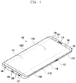
- FIG. 1 is a perspective view illustrating a front surface of an electronic device according to an embodiment.
- FIG. 2 is a perspective view illustrating a rear surface of the electronic device shown in FIG. 1 .
- the mobile electronic device 100 may include a housing 110 including a first surface (or front surface) 110A, a second surface (or rear surface) 110B, and a side surface 110C enclosing a space between the first surface 110A and the second surface 110B.
- the housing may refer to a structure forming some of the first surface 110A, the second surface 110B, and the side surface 110C.
- the first surface 110A may be formed by an at least partially substantially transparent front plate 102 (e.g., a polymer plate or a glass plate including various coating layers).
- the second surface 110B may be formed by a substantially opaque rear plate 111.
- the rear plate 111 may be formed by, for example, coated or colored glass, ceramic, polymer, metal (e.g., aluminum, stainless steel (STS), or magnesium), or a combination of at least two of the above materials.
- the side surface 110C may be coupled to the front plate 102 and the rear plate 111 and be formed by a side bezel structure (or "side member") 118 including a metal and/or a polymer.
- the rear plate 111 and the side bezel structure 118 may be integrally formed and include the same material (e.g., metal material such as aluminum).
- the front plate 102 may include two first regions 110D bent and extended seamlessly from the first surface 110A toward the rear plate 111 at both ends of a long edge of the front plate 102.
- the rear plate 111 may include two second regions 110E bent and extended seamlessly from the second surface 110B towards the front plate 102 at both ends of a long edge.
- the front plate 102 (or the rear plate 111) may include only one of the first regions 110D (or the second regions 110E). In one embodiment, a portion of the first regions 110D or the second regions 110E may not be included.
- the side bezel structure 118 when viewed from the side surface of the mobile electronic device 100, may have a first thickness (or width) at a side surface in which the first region 110D or the second region 110E is not included and have a second thickness smaller than the first thickness at a side surface including the first region 110D or the second region 110E.
- the mobile electronic device 100 may include at least one of a display 101; audio modules 103, 107, and 114; sensor modules 104, 116, and 119; camera modules 105 and 112, key input device 117; light emitting element 106; and connector holes 108 and 109.
- the mobile electronic device 100 may omit at least one (e.g., the key input device 117 or the light emitting element 106) of the components or may further include other components.
- the display 101 may be exposed through, for example, a substantial portion of the front plate 102. In some embodiments, at least part of the display 101 may be exposed through the front plate 102 forming the first region 110D of the side surface 110C and the first surface 110A. In some embodiments, an edge of the display 101 may be formed to be substantially the same as an adjacent outer edge shape of the front plate 102. In one embodiment (not illustrated), in order to enlarge an area where the display 101 is exposed, a distance between an outer edge of the display 101 and an outer edge of the front plate 102 may be formed to be substantially the same.
- a recess or an opening may be formed, and at least one of the audio module 114 and the sensor module 104, the camera module 105, and the light emitting element 106 aligned with the recess or the opening may be included.
- at a rear surface of a screen display area of the display 101 at least one of the audio module 114, the sensor module 104, the camera module 105, the fingerprint sensor module 116, and the light emitting element 106 may be included.
- the display 101 may be coupled to or disposed adjacent to a touch detection circuit, a pressure sensor capable of measuring intensity (pressure) of the touch, and/or a digitizer for detecting a stylus pen of a magnetic field method.
- a touch detection circuit capable of measuring intensity (pressure) of the touch
- a digitizer for detecting a stylus pen of a magnetic field method.
- at least part of the sensor modules 104 and 119 and/or at least part of the key input device 117 may be disposed in a first region 110D and/or a second region 110E.
- the audio modules 103, 107, and 114 may include a microphone hole 103 and speaker holes 107 and 114.
- the microphone hole 103 may dispose a microphone for obtaining an external sound therein; and, in some embodiments, a plurality of microphones may be disposed to detect a direction of a sound.
- the speaker holes 107 and 114 may include an external speaker hole 107 and a call receiver hole 114. In some embodiments, the speaker holes 107 and 114 and the microphone hole 103 may be implemented into one hole, or the speaker may be included without the speaker holes 107 and 114 (e.g., piezo speaker).
- the sensor modules 104, 116, and 119 may generate an electrical signal or a data value corresponding to an operating state inside the mobile electronic device 100 or an environment state outside the mobile electronic device 100.
- the sensor modules 104, 116, and 119 may include, for example, a first sensor module 104 (e.g., proximity sensor) and/or a second sensor module (not illustrated) (e.g., fingerprint sensor), disposed at the first surface 110A of the housing 110, and/or a third sensor module 119 (e.g., a heart rate monitor (HRM) sensor) and/or a fourth sensor module 116 (e.g., fingerprint sensor), disposed at the second surface 110B of the housing 110.
- a first sensor module 104 e.g., proximity sensor
- a second sensor module not illustrated
- a third sensor module 119 e.g., a heart rate monitor (HRM) sensor
- HRM heart rate monitor
- fourth sensor module 116 e.g., fingerprint sensor
- the fingerprint sensor may be disposed at the second surface 110B as well as the first surface 110A (e.g., the display 101) of the housing 110.
- the mobile electronic device 100 may further include a sensor module (not illustrated), for example, at least one of a gesture sensor, gyro sensor, air pressure sensor, magnetic sensor, acceleration sensor, grip sensor, color sensor, IR sensor, biometric sensor, temperature sensor, humidity sensor, and illumination sensor 104.
- the camera modules 105 and 112 may include a first camera device 305 disposed at the first surface 110A of the mobile electronic device 100, a second camera device 112 disposed at the second surface 110B thereof, and/or a flash 113.
- the camera modules 105 and 112 may include one or a plurality of lenses, an image sensor, and/or an image signal processor.
- the flash 113 may include, for example, a light emitting diode or a xenon lamp. In some embodiments, two or more lenses (infrared camera, wide angle and telephoto lens) and image sensors may be disposed at one surface of the mobile electronic device 100.
- the key input device 117 may be disposed at the side surface 110C of the housing 110.
- the mobile electronic device 100 may not include some or all of the above-described key input devices 117, and the key input device 117 that is not included may be implemented in other forms such as a soft key on the display 101.
- the key input device 117 may include a sensor module 116 disposed at the second surface 110B of the housing 110.
- the light emitting element 106 may be disposed at, for example, the first surface 110A of the housing 110.
- the light emitting element 106 may provide, for example, status information of the mobile electronic device 100 in an optical form.
- the light emitting element 106 may provide, for example, a light source interworking with an operation of the camera module 105.
- the light emitting element 106 may include, for example, a light emitting diode (LED), an IR LED, and a xenon lamp.
- the connector ports 108 and 109 may include a first connector port 108 that may receive a connector (e.g., a USB connector) for transmitting and receiving power and/or data to and from an external electronic device and/or a second connector hole (e.g., earphone jack) 109 that can receive a connector for transmitting and receiving audio signals to and from an external electronic device.
- a connector e.g., a USB connector
- a second connector hole e.g., earphone jack
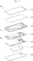
- FIG. 3 is an exploded perspective view illustrating the electronic device 100 shown in FIG. 1 .
- the mobile electronic device 300 may include a side bezel structure 310(e.g. part of side surface 110C of FIG. 1 ), first support member 311 (e.g., bracket), front plate 320, display 330(e.g. display101 of FIG. 1 ) , printed circuit board 340, battery 350, second support member 360 (e.g., rear case), antenna 370, and rear plate 380.
- the electronic device 300 may omit at least one (e.g., the first support member 311 or the second support member 360) of the components or may further include other components. At least one of the components of the electronic device 300 may be the same as or similar to at least one of the components of the mobile electronic device 300 of FIG. 1 or 2 and a duplicated description is omitted below.
- the first support member 311 may be disposed inside the electronic device 300 to be connected to the side bezel structure 310 or may be integrally formed with the side bezel structure 310.
- the first support member 311 may be made of, for example, a metal material and/or a non-metal (e.g., polymer) material.
- the display 330 may be coupled to one surface thereof, and the printed circuit board 340 may be coupled to the other surface thereof.
- a processor, a memory, and/or an interface may be mounted.
- the processor may include, for example, one or more of a central processing unit, application processor, graphic processing unit, image signal processor, sensor hub processor, or communication processor.
- the printed circuit board 340 may include, for example, a conductive member (e.g. a clip part) electrically connected to the side bezel structure 310, and contact at least a portion of the side bezel structure 310.
- a guide member e.g. a protruding guide
- the memory may include, for example, a volatile memory or a nonvolatile memo ry.
- the interface may include, for example, a HDMI, USB interface, SD card interface, and/or audio interface.
- the interface may, for example, electrically or physically connect the electronic device 300 to an external electronic device and include a USB connector, an SD card/ multimedia card (MMC) connector, or an audio connector.
- MMC multimedia card
- the battery 350 is a device for supplying power to at least one component of the electronic device 300 and may include, for example, a non-rechargeable primary battery, a rechargeable secondary battery, or a fuel cell. At least part of the battery 350 may be disposed, for example, on substantially the same plane as that of the printed circuit board 340.
- the battery 350 may be integrally disposed inside the electronic device 300 or may be detachably disposed in the electronic device 300.
- the antenna 370 may be disposed between the rear plate 380 and the battery 350.
- the antenna 370 may include, for example, a near field communication (NFC) antenna, wireless charging antenna, and/or magnetic secure transmission (MST) antenna.
- the antenna 370 may perform, for example, short range communication with an external device or may wirelessly transmit and receive power required for charging.
- an antenna structure may be formed by some or a combination of the side bezel structure 310 and/or the first support member 311.
- at least a part of the side bezel structure 310 may be electrically connected to a conductive member (e.g., a clip part) to form an antenna area.
- FIG. 4A is a plan view illustrating a part of a housing according to various embodiments of the disclosure
- FIG. 4B is a perspective view illustrating a part of the housing shown in FIG. 4A
- FIG. 4C is an enlarged perspective view illustrating a part of the housing shown in FIG. 4A .
- the electronic device e.g., the electronic device 100 in FIG. 1
- the electronic device 100 of this embodiment may include a housing (e.g., the housing 110 in FIG. 1 ) in which components included in the electronic device are accommodated, combined, or installed.
- FIG. 4A may illustrate a certain part of a housing 400 according to various embodiments.
- the part of the housing 400 shown in FIG. 4A may be a part including side portions of the electronic device having a rectangular form.
- the housing 400 may have a region formed of a conductive material.
- at least a partial region of the housing 400 may be formed of a metal material.
- the housing 400 may be segmented into a plurality of regions.
- the housing 400 may be formed generally of a metal material, and a partial region of the housing 400 may be formed of an insulating material, so that the housing 400 may be segmented into a plurality of regions electrically disconnected from each other.
- the housing 400 has a mounting portion 410 formed to allow a printed circuit board (e.g., the printed circuit board 340 in FIG. 3 or the printed circuit board 500 in FIG. 5A ) to be mounted.
- the mounting portion 410 of the housing 400 may be formed in a shape substantially corresponding to the printed circuit board so that the printed circuit board can be mounted thereon.
- the mounting portion 410 may have an area similar to or greater than that of the printed circuit board.
- the housing 400 may have an inner wall portion 420 extending from the mounting portion 410.
- the inner wall portion 420 may be formed to extend in a first direction with respect to the mounting portion 410.
- the first direction may be the positive Z direction with reference to FIG. 4B .
- the inner wall portion 420 extending in the first direction with respect to the mounting portion 410 may be one of side portions of the housing 400.
- the inner wall portion 420 may be formed of the same material as the housing 400.
- the extending length of the inner wall portion 420 or the height of the inner wall portion 420 may be determined depending on the size or volume of electronic components mounted on the mounting portion 410 of the housing 400.
- a guide groove 430 may be formed in the inner wall portion 420 of the housing 400.
- the guide groove 430 may be concavely formed in the inner wall portion 420.
- the guide groove 430 may be formed in the inner wall portion 420 to be concave in the negative X direction of FIG. 4B .
- a protrusion guide e.g., the protrusion guide 530 in FIG. 5A
- the guide groove 430 may be formed to substantially correspond to the protrusion guide 530.
- the length and width of the guide groove 430 may be determined depending on the shape of the protrusion guide 530.
- the shape of the guide groove 430 may be determined in consideration of various design factors.
- a guide portion may be formed on the inner wall portion 420 of the housing 400.
- the guide portion (not shown) may be convexly formed on the inner wall portion 420.
- the guide portion (not shown) may be formed on the inner wall portion 420 to be convex in the positive X direction of FIG. 4B , and it may be engaged with the printed circuit board (e.g., the printed circuit board 340 in FIG. 3 or the printed circuit board 500 in FIG. 5A ).
- the length and width of the guide portion (not shown) may be determined depending on the shape of an engaging portion (not shown) of the printed circuit board.
- the shape of the guide portion (not shown) may be determined in consideration of various design factors.
- a pad portion 440 formed of a conductive material may be disposed on at least a portion of the inner wall portion 420 of the housing 400.
- the pad portion 440 may contact a clip portion (e.g., the clip portion 521 in FIG. 5A ) of a clip member (e.g., the clip member 520 in FIG. 5A ) to be described later.
- an opening portion 460 may be formed in at least a part of the inner wall portion 420 of the housing 400.
- a connector e.g., the connector 540 in FIG. 5A
- the opening portion 460 may be formed in the inner wall portion 420 in a shape substantially corresponding to the connector.
- a shoulder portion 470 that protrudes in a direction (e.g., the positive X direction in FIG. 4B ) from the inner wall portion 420 toward the mounting portion 410 may be formed on the inner wall portion 420 adjacent to the opening portion 460.
- the shoulder portion 470 may be formed to start from the inner wall portion 420 adjacent to the opening portion 460 in the first direction (e.g., the positive Z direction in FIG. 4B ) and protrude in a direction toward the mounting portion 410.
- the shape (e.g., length) of the shoulder portion 470 protruding in the direction e.g., the positive X direction in FIG.
- the length of the shoulder portion 470 may refer to a length (e.g., HI in FIG. 4A ) from the inner wall portion 420 to the end of the shoulder portion 470.
- the length of the shoulder portion 470 may be greater than the length (e.g., H2 in FIG. 5B ) at which the clip portion (e.g., the clip portion 521 in FIG. 5A ) protrudes in the negative X direction.
- the connector coupled to the printed circuit board may be caught by the shoulder portion 470.
- the shoulder portion 470 may limit an assembly flow so that the printed circuit board is approaching in a state of being spaced apart from the inner wall portion 420 of the housing 400.
- the printed circuit board may need to approach the housing 400 in the second direction in a state of being spaced apart from the inner wall portion 420 of the housing 400 in the positive X direction shown in FIG. 4B .
- the housing 400 may not include the shoulder portion 470.
- FIG. 5A is a perspective view illustrating a printed circuit board according to various embodiments of the disclosure
- FIG. 5B is a plan view illustrating the printed circuit board shown in FIG. 5A .
- a printed circuit board 500 shown in FIG. 5A may be mounted on the mounting portion 410 of the housing 400 shown in FIG. 4A .
- electronic components performing various functions may be mounted on and electrically connected to the printed circuit board 500.
- a connector 540 and a clip member 520 may be installed on the printed circuit board 500.
- the electronic components installed on the printed circuit board 500 may be electrically connected by conductive lines formed on the printed circuit board 500 in a printed manner.
- the printed circuit board 500 shown in FIG. 5A may be one of printed circuit boards included in the electronic device (e.g., the electronic device 101 in FIG. 1 ).
- the printed circuit board 500 may include an outer wall portion 510.
- the outer wall portion 510 refers to one side surface of the printed circuit board 500 disposed substantially parallel to the inner wall portion 420 of the housing 400 in a state where the printed circuit board 500 is mounted on the mounting portion 410 of the housing 400.
- the inner wall portion 420 of the housing 400 and the outer wall portion 510 of the printed circuit board 500 may be in a state of facing each other at least in part.
- the clip member 520 installed on the printed circuit board 500 may transmit an electrical signal moving through the conductive line printed on the printed circuit board 500 to a component in contact with the clip portion 521 of the clip member 520 or transmit an electrical signal of a component in contact with the clip portion 521 of the clip member 520 to the conductive line printed on the printed circuit board 500.
- the clip member 520 may transmit an antenna signal.
- the clip member 520 may be electrically connected to an antenna feed (not shown) or a ground (not shown) for generating or receiving an antenna signal.
- the clip member 520 may be disposed at a position adjacent to the outer wall portion 510 of the printed circuit board 500.
- the clip portion 521 of the clip member 520 may be formed to protrude toward the inner wall portion 420 of the housing 400 (e.g., in the negative X direction in FIG. 5A ). In a state where the printed circuit board 500 is mounted on the mounting portion 410 of the housing 400, the clip portion 521 of the clip member 520 may contact the inner wall portion 420 of the housing 400. In case that the pad portion 440 is disposed on the inner wall portion 420 of the housing 400, the clip portion 521 may contact the pad portion 440.
- a plurality of clip portions 521 and clip members 520 may be provided and arranged along the outer wall portion 510 of the printed circuit board 500.
- the connector 540 installed on the printed circuit board 500 may include a universal serial bus (USB) connector 540.
- the connector 540 may be a USB C-type connector 540.
- the connector 540 may be used for a wired connection between an external electronic device and the electronic device.
- the connector 540 may be disposed at a position adjacent to the outer wall portion 510 of the printed circuit board 500. At least a part of the connector 540 may protrude toward the inner wall portion 420 of the housing 400 (e.g., in the negative X direction in FIG. 5A ).
- the connector 540 may be inserted into an opening portion (e.g., the opening portion 460 in FIG. 4A ) formed in the inner wall portion 420 of the housing 400 described above. In a state where the connector 540 is inserted into the opening portion 460, the connector 540 may be exposed at least in part to the outside of the electronic device.
- a protrusion guide 530 may be formed on the printed circuit board 500.
- the protrusion guide 530 may protrude in substantially the same direction as the clip portion 521 of the clip member 520 (e.g., the negative X direction in FIG. 5A ).
- the protrusion guide 530 may start from the outer wall portion 510 of the printed circuit board 500 and extend toward the inner wall portion 420 of the housing 400.
- the protrusion guide 530 may be formed at a position spaced apart from the clip portion 521 of the clip member 520 in the second direction (e.g., the negative Z direction in FIG. 5A ).
- a protrusion degree of the protrusion guide 530 may be greater than a protrusion degree of the clip portion 521.
- a length (e.g., L1 in FIG. 8C ) from the outer wall portion 510 of the printed circuit board 500 to the end of the protrusion guide 530 may be greater than a length (e.g., L2 in FIG.
- the protrusion guide 530 may be formed at a position spaced apart from the clip portion 521 of the clip member 520 in the third direction (e.g., the positive Z direction in FIG. 5A ).
- the protrusion guide 530 may be formed integrally with the printed circuit board 500.
- the protrusion guide 530 may refer to a portion protruding from the outer wall portion 510 of the printed circuit board 500.
- the protrusion guide may be a separate component installed on the printed circuit board.
- the protrusion guide installed on the printed circuit board may protrude toward the inner wall portion 420 of the housing 400.
- the shape of the protrusion guide 530 may be formed to be substantially engaged with the shape of the guide groove (e.g., the guide groove 430 in FIG. 4B ).
- the protrusion guide 530 may be formed in a semicircular shape so that the guide groove and the protrusion guide are engaged (e.g., contacted).
- the protrusion guide 530 may be formed in various shapes (e.g., semicircular, oval, square, asymmetrical, etc.) to facilitate the process of assembling the printed circuit board 500 with respect to the housing 400 by a worker.
- the protrusion guide 530 may be disposed at a position adjacent to at least one of the clip portion 521 and the clip member 520.
- the protrusion guide 530 may be formed to protrude toward (e.g., in the negative X direction in FIG. 5A ) the inner wall portion 420 of the housing 400 from the end of the outer wall portion 510 of the printed circuit board 500 or the edge portion of the printed circuit board 500.
- the end of the outer wall portion 510 or the edge portion may refer to an end portion of the outer wall portion 510 in the extension direction of the outer wall portion 510 (e.g., the positive/negative Y axis directions in FIG. 5A ).
- the outer wall portion 510 may be one side surface of the printed circuit board 500 substantially facing the inner wall portion 420 of the housing 400, so the end of the outer wall portion 510 or the edge portion may refer to both ends of one side surface of the printed circuit board 500 facing the inner wall portion 420 of the housing 400.
- the protrusion guide 530 may be inserted into the guide groove 430 formed in the inner wall portion 420 of the housing 400.
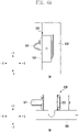
- FIGS. 6A and 6B are views illustrating clip members according to various embodiments of the disclosure.
- (a) shows plan views of the clip member, and (b) shows side views of the clip member.
- the clip member 520 or 620 may include a body portion 522 or 622 and a clip portion 521 or 621.
- the body portion 522 or 622 may be installed on the printed circuit board 500.
- the body portion 522 or 622 installed on the printed circuit board 500 allows the clip member 520 or 620 to be fixed on the printed circuit board 500.
- the clip portion 521 or 621 is mounted on the printed circuit board 500 and may transmit an electrical signal moving through a conductive line printed on the printed circuit board 500 to a component in contact with the clip portion 521 or 621 or transmit an electrical signal of a component in contact with the clip portion 521 or 621 to a conductive line printed on the printed circuit board 500.
- the clip member 520 shown in FIG. 6A will be referred to as a first clip member 520
- the clip portion included in the first clip member 520 will be referred to as a first clip portion 521
- the body portion included in the first clip member 520 will be referred to as a first body portion 522
- the clip member 620 shown in FIG. 6B will be referred to as a second clip member 620
- the clip portion included in the second clip member 620 will be referred to as a second clip portion 621
- the body portion included in the second clip member 620 will be referred to as a second body portion 622.
- the clip portions 521 and 621 of the clip members 520 and 622 may be pressed against the inner wall portion 420 of the housing 400 and thereby elastically deformed.
- the first clip portion 521 may be formed to extend in a direction (e.g., the positive/negative Y axis directions in FIG. 6A ) parallel to the extending direction of the printed circuit board 500.
- a part of the first clip portion 521 may be bent, and both ends of the first clip portion 521 may be installed on the first body portion 522.
- the shape of the first clip portion 521 is not limited to the illustrated embodiment, and according to various embodiments, the shape of the first clip portion 521 may vary.
- the first clip portion 521 may have, but not limited to, a shape bent once, but it may be bent multiple times (e.g., three times) or formed in a concave-convex shape.
- the second clip portion 621 may be formed to extend in a direction (e.g., the positive/negative Z axis directions in FIG. 6B ) perpendicular to the extending direction of the printed circuit board 500.
- a part of the second clip portion 621 may be bent, and both ends of the second clip portion 621 may be installed on the second body portion 622.
- the height A of the first clip member 520 may be lower than the height B of the second clip member 620.
- the height may refer to the length A or B from the surface of the printed circuit board 500 to the point where the body portion 522 or 622 of the clip member 520 or 620 ends.
- the thickness of the electronic device may be reduced compared to a case where the second clip member 620 is used.
- the second clip portion 621 may have an inclined surface formed in the Z-axis direction by bending.
- the second clip portion 621 may be gradually pressed against the inner wall portion 420 of the housing 400.
- the first clip portion 521 may have an inclined surface formed in the Y-axis direction by bending. In case that the printed circuit board 500 approaches the mounting portion 410 of the housing 400 in the second direction (e.g., the negative Z direction in (b) of FIG.
- the first clip portion 521 may be damaged by being caught on the inner wall portion 420 of the housing 400.
- the clip member 520 including the first clip portion 521 may have the risk of being damaged, depending on an approach direction of the printed circuit board 500 including the clip member 520 toward the housing 400 caused by a worker.
- the electronic device and the printed circuit board 500 included therein can prevent damage to the clip member 520 including the clip portion 521 shaped such as the first clip portion 521 in the process of assembling the printed circuit board 500 with respect to the housing 400 by a worker.
- FIG. 7 is a view illustrating an assembly aspect of a housing and a printed circuit board according to various embodiments of the disclosure
- FIGS. 8A to 8C are views illustrating an assembly aspect of a housing and a printed circuit board according to various embodiments of the disclosure
- FIGS. 9A and 9B are views illustrating a state of assembling a housing and a printed circuit board according to various embodiments of the disclosure.
- At least one of components of the housing and the printed circuit board in FIGS. 7 to 9B may be similar to at least one of the components of the housing and the printed circuit board in FIGS. 4A to 6B , so overlapping descriptions may be omitted hereinafter.
- the protrusion length of the shoulder portion 470 protruding at a position adjacent to the opening portion 460 formed in the inner wall portion 420 may be greater than the protrusion length of the clip portion 521 of the clip member 520.
- the protrusion length of the shoulder portion 470 may refer to the length (e.g., HI in FIG. 4A ) from the inner wall portion 420 to the end of the shoulder portion 470
- the protrusion length of the clip portion 521 may refer to the length (e.g., H2 in FIG. 5B ) from the body portion 522 of the clip member 520 to the end of the clip portion 521.
- the printed circuit board 500 may have to be put in the second direction (e.g., the negative Z direction in FIG. 7 ) in a state where the outer wall portion 510 of the printed circuit board 500 is spaced apart from the inner wall portion 420 of the housing 400 in the positive X direction in FIG. 7 .
- the second direction e.g., the negative Z direction in FIG. 7
- the protrusion length of the shoulder portion 470 is greater than the protrusion length of the clip portion 521, it is possible to prevent the clip portion 521 of the clip member 520 from being caught and damaged by the inner wall portion 420 of the housing 400 when the outer wall portion 510 of the printed circuit board 500 is spaced apart from the inner wall portion 420 of the housing 400 to such an extent that the connector 540 is not caught on the shoulder portion 470.
- the printed circuit board 500 may approach the mounting portion 410 of the housing 400 in the second direction.
- the connector 540 may not be caught on the shoulder portion 470, and only the clip portion 521 may be caught on the inner wall portion 420 of the housing 400.
- the protrusion guide 530 may be formed to protrude from a position spaced apart from the clip portion 521 in the second direction.
- the protrusion guide 530 may first contact the inner wall portion 420 of the housing 400. In a state where the protrusion guide 530 is caught on the inner wall portion 420 of the housing 400, the printed circuit board 500 may be difficult to move in the second direction. A worker may move the printed circuit board 500 in the second direction in a state where the outer wall portion 510 of the printed circuit board 500 is spaced apart from the inner wall portion 420 of the housing 400. For this reason, the risk that the clip portion 521 is caught and damaged by the inner wall portion 420 may be reduced.
- the printed circuit board 500 may allow assembly through other assembly path (e.g., moving the printed circuit board 500 in the second direction in a state where the outer wall portion 510 and the inner wall portion 420 are spaced apart) than a worker's assembly path (e.g., putting the printed circuit board 500 into the housing 400 in the second direction in a state where the outer wall portion 510 and the inner wall portion 420 are parallel). Therefore, it is possible to prevent damage to the clip portion 521 that may be caused in the process of assembling the printed circuit board 500 and the housing 400.
- assembly path e.g., moving the printed circuit board 500 in the second direction in a state where the outer wall portion 510 and the inner wall portion 420 are spaced apart
- a worker's assembly path e.g., putting the printed circuit board 500 into the housing 400 in the second direction in a state where the outer wall portion 510 and the inner wall portion 420 are parallel. Therefore, it is possible to prevent damage to the clip portion 521 that may be caused in the process of assembling the printed
- the position at which the guide groove 430 is formed in the inner wall portion 420 of the housing 400 may be determined as a position where the clip portion 521 of the clip member 520 is not caught and not damaged by the inner wall portion 420 of the housing 400 even when the protrusion guide 530 is inserted into the guide groove 430. Because the protrusion guide 530 is formed to protrude further than the clip portion 521 and formed to be spaced apart from the clip portion 521 in the second direction, the clip portion 521 may not contact the inner wall portion 420 of the housing 400 until the protrusion guide 530 is inserted into the guide groove 430. The protrusion guide 530 may prevent the clip portion 521 from being caught and damaged by the inner wall portion 420 of the housing 400.
- the protrusion guide 530 may prevent the clip portion 521 of the clip member 520 from contacting the inner wall portion 420 of the housing 400 until it is inserted into the guide groove 430.
- the guide groove 430 may be formed at a position of accommodating the protrusion guide 530.
- the clip portion 521 of the clip member 520 may be elastically deformed by contacting the contact surface 421 of the inner wall portion 420. Therefore, when the clip portion 521 starts to come into contact with the contact surface 421 of the inner wall portion 420, the risk that the clip portion 521 is caught and damaged by the inner wall portion 420 can be reduced.
- the clip portion 521 may not be caught and not be damaged by the inner wall portion 420.
- the formation position of the guide groove 430 may be determined such that the distance B from the end of the inner wall portion 420 to the start portion of the guide groove 430 is greater than the distance A between the protrusion guide 530 and the clip portion 521.
- the formation position of the guide groove 430 is determined in this way, the clip portion 521 may not be caught on the inner wall portion 420 before the protrusion guide 530 is inserted into the guide groove 430.
- the clip portion 521 of the clip member 520 may be in contact with the pad portion 440 disposed on the inner wall portion 420 of the housing 400. In another embodiment, the clip portion 521 of the clip member 520 may directly contact the inner wall portion 420 of the housing 400.
- the connector 540 may be inserted into the opening portion 460 formed in the inner wall portion 420.
- the protrusion guide 530 may be inserted into the guide groove 430.
- a position at which the guide groove 430 is formed may be determined such that a separation distance (e.g., C in FIG. 9B ) between the guide groove 430 and the protrusion guide 530 is smaller than a distance (e.g., D in FIG. 9B ) from a lower surface of the clip portion 521 to an upper surface of the clip member 520 in a state where the printed circuit board 500 is mounted on the mounting portion 410.
- a separation distance e.g., C in FIG. 9B
- an electronic device may include a housing including a mounting portion and an inner wall portion extending in a first direction with respect to the mounting portion; a printed circuit board mounted on the mounting portion of the housing and including an outer wall portion disposed substantially parallel to the inner wall portion of the housing in a state of being mounted on the mounting portion of the housing; a clip member disposed at a position adjacent to the outer wall portion of the printed circuit board, electrically connected to the printed circuit board, and including a clip portion formed to protrude toward the inner wall portion to be in contact with the inner wall portion; a protrusion guide spaced apart from the clip portion in a second direction opposite to the first direction and formed to protrude from the outer wall portion of the printed circuit board toward the inner wall portion of the housing; and a guide groove formed in the inner wall portion of the housing to accommodate the protrusion guide in a state where the printed circuit board is mounted on the mounting portion of the housing.
- the protrusion guide may be formed integrally with the printed circuit board.
- the protrusion guide may be disposed at a position adjacent to the clip member.
- the protrusion guide may be disposed on an edge portion of the outer wall portion of the printed circuit board.
- the clip member may include a body portion installed on the printed circuit board, and the clip portion may extend in a direction parallel to the extending direction of the printed circuit board, be bent at least in part, and be fixed to the body portion at both ends thereof.
- the clip portion may be elastically deformed in contact with the inner wall portion of the housing.
- the electronic device may further include a connector disposed at a position adjacent to the outer wall portion of the printed circuit board and electrically connected to the printed circuit board; and an opening portion formed in the inner wall portion of the housing to receive the connector in a state where the printed circuit board is mounted on the mounting portion of the housing.
- the electronic device may further include a shoulder portion adjacent to the opening portion in the first direction and protruding from the inner wall portion of the housing in a mounting direction of the printed circuit board.
- the protrusion length of the shoulder portion may be greater than the protrusion length of the clip portion.
- a formation position of the guide groove may be determined such that the protrusion guide is inserted into the guide groove at a position where the clip portion is elastically deformed by the inner wall portion of the housing.
- the electronic device may further include a pad portion disposed at least in part on the inner wall portion of the housing, wherein the clip portion is elastically deformed in contact with the pad portion.
- a printed circuit board may include an outer wall portion formed in the printed circuit board to be disposed substantially parallel to an inner wall portion of a housing, the inner wall portion extending in a first direction with respect to a mounting portion of the housing; a clip member disposed at a position adjacent to the outer wall portion, electrically connected to the printed circuit board, and including a clip portion formed to protrude toward the inner wall portion of the housing to be in contact with the inner wall portion; and a protrusion guide spaced apart from the clip portion in a second direction opposite to the first direction, formed to protrude from the outer wall portion toward the inner wall portion of the housing, and inserted into a guide groove formed in the inner wall portion of the housing, wherein the printed circuit board may be mounted at least in part on the mounting portion of the housing.
- the protrusion guide may be formed integrally with the printed circuit board.
- the protrusion guide may be disposed at a position adjacent to the clip member.
- the protrusion guide may be disposed on an edge portion of the outer wall portion.
- the clip member may include a body portion installed on the printed circuit board, and the clip portion may extend in a direction parallel to the extending direction of the printed circuit board, be bent at least in part, and be fixed to the body portion at both ends thereof.
- the clip portion may be elastically deformed in contact with the inner wall portion of the housing.
- the printed circuit board may further include a connector disposed at a position adjacent to the outer wall portion, electrically connected to the printed circuit board, and inserted into the opening portion formed in the inner wall portion of the housing.
- an electronic device may include a front plate forming a first surface of the electronic device, a display exposed to the outside of the electronic device in a first direction through at least a portion of the front plate, a rear plate forming a second surface of the electronic device opposite to the first surface, a side bezel structure including a first support member combined at least in part with the display and disposed between the front and rear plates to be combined with the front and rear plates, a printed circuit board including a clip portion formed to be electrically connected to the side bezel structure and combined with the first support member, and a protrusion guide formed on the printed circuit board to be spaced apart from the clip portion in a second direction opposite to the first direction and protruding toward the side bezel structure, wherein at least a partial area of the side bezel structure may be electrically connected to the clip portion to form an antenna area.
- the side bezel structure may include a guide groove formed in at least a part of the side bezel structure to receive the protrusion guide.
Landscapes
- Engineering & Computer Science (AREA)
- Signal Processing (AREA)
- Computer Hardware Design (AREA)
- Microelectronics & Electronic Packaging (AREA)
- General Engineering & Computer Science (AREA)
- Theoretical Computer Science (AREA)
- Human Computer Interaction (AREA)
- Physics & Mathematics (AREA)
- General Physics & Mathematics (AREA)
- Computer Networks & Wireless Communication (AREA)
- Casings For Electric Apparatus (AREA)
- Production Of Multi-Layered Print Wiring Board (AREA)
Applications Claiming Priority (2)
| Application Number | Priority Date | Filing Date | Title |
|---|---|---|---|
| KR1020200012615A KR102711476B1 (ko) | 2020-02-03 | 2020-02-03 | 인쇄 회로 기판을 포함하는 전자 장치 |
| PCT/KR2021/001417 WO2021158011A1 (ko) | 2020-02-03 | 2021-02-03 | 인쇄 회로 기판을 포함하는 전자 장치 |
Publications (3)
| Publication Number | Publication Date |
|---|---|
| EP4087220A1 true EP4087220A1 (de) | 2022-11-09 |
| EP4087220A4 EP4087220A4 (de) | 2023-07-05 |
| EP4087220B1 EP4087220B1 (de) | 2026-04-01 |
Family
ID=77200263
Family Applications (1)
| Application Number | Title | Priority Date | Filing Date |
|---|---|---|---|
| EP21750963.7A Active EP4087220B1 (de) | 2020-02-03 | 2021-02-03 | Elektronische vorrichtung mit leiterplatte |
Country Status (5)
| Country | Link |
|---|---|
| US (1) | US20220374051A1 (de) |
| EP (1) | EP4087220B1 (de) |
| KR (2) | KR102711476B1 (de) |
| CN (1) | CN115066875B (de) |
| WO (1) | WO2021158011A1 (de) |
Families Citing this family (3)
| Publication number | Priority date | Publication date | Assignee | Title |
|---|---|---|---|---|
| KR20230040521A (ko) * | 2021-09-16 | 2023-03-23 | 삼성전자주식회사 | 밀리미터파 안테나 모듈 배치 구조를 포함하는 전자장치 |
| WO2024010180A1 (ko) * | 2022-07-06 | 2024-01-11 | 삼성전자 주식회사 | 지지 부재를 포함하는 전자 장치 |
| CN117715327A (zh) * | 2022-09-06 | 2024-03-15 | 苏州佳世达电通有限公司 | 可自动切换其操作模式的电子装置 |
Family Cites Families (26)
| Publication number | Priority date | Publication date | Assignee | Title |
|---|---|---|---|---|
| JP3402435B2 (ja) * | 1997-05-09 | 2003-05-06 | 住友電装株式会社 | プリント基板用コネクタ |
| JP4102747B2 (ja) * | 2003-12-01 | 2008-06-18 | 日本圧着端子製造株式会社 | コネクタ |
| KR100586995B1 (ko) * | 2004-09-14 | 2006-06-08 | 삼성전자주식회사 | 디스플레이장치 |
| JP4884746B2 (ja) * | 2005-10-20 | 2012-02-29 | 株式会社 日立ディスプレイズ | 液晶表示装置 |
| JP2007157357A (ja) * | 2005-11-30 | 2007-06-21 | Toshiba Corp | カードエッジコネクタ、電子回路基板並びに電子機器 |
| KR20120019139A (ko) * | 2010-08-25 | 2012-03-06 | 삼성전자주식회사 | 액정표시장치 |
| KR101709532B1 (ko) * | 2010-11-11 | 2017-02-24 | 엘지전자 주식회사 | 이동 단말기 |
| KR101978210B1 (ko) * | 2012-09-25 | 2019-05-14 | 엘지전자 주식회사 | 이동 단말기 |
| JP6096046B2 (ja) * | 2013-05-08 | 2017-03-15 | シャープ株式会社 | 電子機器 |
| KR102208686B1 (ko) * | 2014-08-11 | 2021-01-28 | 삼성전자주식회사 | 전자 장치 및 그 제작 방법 |
| KR20160127542A (ko) * | 2015-04-27 | 2016-11-04 | 엘지전자 주식회사 | 이동단말기 |
| KR101726698B1 (ko) * | 2015-07-29 | 2017-04-13 | 주식회사 고아정공 | 모터 |
| CN205039288U (zh) * | 2015-08-27 | 2016-02-17 | 泰科电子(上海)有限公司 | 连接器 |
| KR20170037464A (ko) * | 2015-09-25 | 2017-04-04 | 엘지전자 주식회사 | 이동 단말기 |
| KR102507947B1 (ko) * | 2015-10-15 | 2023-03-09 | 삼성전자주식회사 | 케이스 및 이를 포함하는 전자 장치 |
| KR102400529B1 (ko) * | 2015-10-26 | 2022-05-20 | 삼성전자주식회사 | 금속 케이스를 구비한 전자기기 및 이에 사용되는 금속 케이스 |
| KR102473376B1 (ko) * | 2016-04-01 | 2022-12-05 | 삼성전자주식회사 | 인쇄회로기판 및 이를 포함하는 전자 장치 |
| KR101759950B1 (ko) * | 2016-06-24 | 2017-07-20 | 엘지전자 주식회사 | 이동 단말기 |
| KR102528424B1 (ko) * | 2016-08-31 | 2023-05-04 | 삼성전자주식회사 | 전자 부품 및 그를 포함하는 전자 장치 |
| JP6814607B2 (ja) * | 2016-11-11 | 2021-01-20 | 三菱重工サーマルシステムズ株式会社 | 電動圧縮機 |
| KR102295668B1 (ko) * | 2017-04-12 | 2021-08-30 | 삼성전자주식회사 | 도전성 경로를 가지는 지지 구조물 및 이를 포함하는 전자 장치 |
| CN207022335U (zh) * | 2017-08-15 | 2018-02-16 | 新华三技术有限公司 | 电子设备及导向销 |
| KR102503982B1 (ko) * | 2018-02-23 | 2023-02-28 | 삼성전자주식회사 | 휘어진 상태로 유지되는 가요성 회로기판을 포함하는 카메라 모듈 어셈블리 및 이를 포함하는 전자 장치 |
| KR102411482B1 (ko) * | 2018-06-11 | 2022-06-22 | 삼성전자 주식회사 | 용량성 구조물을 포함하는 전자 장치 |
| KR102544860B1 (ko) * | 2018-06-27 | 2023-06-19 | 삼성전자 주식회사 | 안테나 클립 및 이를 포함하는 전자장치 |
| CN208798002U (zh) * | 2018-10-16 | 2019-04-26 | Oppo(重庆)智能科技有限公司 | 显示面板、显示屏组件以及电子装置 |
-
2020
- 2020-02-03 KR KR1020200012615A patent/KR102711476B1/ko active Active
-
2021
- 2021-02-03 WO PCT/KR2021/001417 patent/WO2021158011A1/ko not_active Ceased
- 2021-02-03 CN CN202180012800.3A patent/CN115066875B/zh active Active
- 2021-02-03 EP EP21750963.7A patent/EP4087220B1/de active Active
-
2022
- 2022-08-02 US US17/879,130 patent/US20220374051A1/en active Pending
-
2024
- 2024-09-24 KR KR1020240129348A patent/KR20240147641A/ko active Pending
Also Published As
| Publication number | Publication date |
|---|---|
| US20220374051A1 (en) | 2022-11-24 |
| WO2021158011A1 (ko) | 2021-08-12 |
| KR20240147641A (ko) | 2024-10-08 |
| EP4087220A4 (de) | 2023-07-05 |
| CN115066875A (zh) | 2022-09-16 |
| CN115066875B (zh) | 2025-05-06 |
| KR20210098722A (ko) | 2021-08-11 |
| EP4087220B1 (de) | 2026-04-01 |
| KR102711476B1 (ko) | 2024-09-27 |
Similar Documents
| Publication | Publication Date | Title |
|---|---|---|
| EP3763110B1 (de) | Elektronische vorrichtung mit gehäuse und verfahren zur herstellung des gehäuses | |
| KR102661196B1 (ko) | 적층형 기판을 포함하는 전자 장치 | |
| EP3741099B1 (de) | Leitungsstruktur einer elektronischen vorrichtung und elektronische vorrichtung damit | |
| US20220374051A1 (en) | Electronic device including printed circuit board | |
| KR102763578B1 (ko) | 카메라 모듈을 포함하는 전자 장치 | |
| KR102920992B1 (ko) | 인터페이스 단자를 포함하는 전자 장치 | |
| KR20210133645A (ko) | 연결 부재를 구비하는 연성 회로 기판을 포함하는 전자 장치 | |
| US20210006648A1 (en) | Electrical connection device and electronic device comprising same | |
| KR20200139977A (ko) | 지지 부재의 도전 구조를 포함하는 전자 장치 | |
| EP4117407A1 (de) | Elektronische vorrichtung mit abschirmungselement zur abschirmung von mindestens einem teil einer magnetischen, durch eine magnetische substanz erzeugten kraft und verbindungsabschnitt mit der eigenschaft der nichtmagnetischen, mit dem abschirmungselement verbundenen substanz | |
| US12237564B2 (en) | Antenna and electronic device including same | |
| EP4319110B1 (de) | Elektronische vorrichtung mit elektrischem verbindungselement | |
| EP3755133B1 (de) | Elektronische vorrichtung mit abschirmdosenstruktur | |
| EP4271149B1 (de) | Elektronische vorrichtung mit wasserdichter struktur | |
| KR102951640B1 (ko) | 트레이 소켓 및 이를 포함하는 전자 장치 | |
| US12604423B2 (en) | Electronic device including camera module | |
| EP4572027A1 (de) | Elektronische vorrichtung mit elektrischer verbindungsstruktur | |
| EP4546761A1 (de) | Elektronische vorrichtung mit befestigungselement | |
| KR20240117964A (ko) | 카메라 모듈을 포함하는 전자 장치 | |
| KR20250053655A (ko) | 전기적 연결 구조를 포함하는 전자 장치 |
Legal Events
| Date | Code | Title | Description |
|---|---|---|---|
| STAA | Information on the status of an ep patent application or granted ep patent |
Free format text: STATUS: THE INTERNATIONAL PUBLICATION HAS BEEN MADE |
|
| PUAI | Public reference made under article 153(3) epc to a published international application that has entered the european phase |
Free format text: ORIGINAL CODE: 0009012 |
|
| STAA | Information on the status of an ep patent application or granted ep patent |
Free format text: STATUS: REQUEST FOR EXAMINATION WAS MADE |
|
| 17P | Request for examination filed |
Effective date: 20220803 |
|
| AK | Designated contracting states |
Kind code of ref document: A1 Designated state(s): AL AT BE BG CH CY CZ DE DK EE ES FI FR GB GR HR HU IE IS IT LI LT LU LV MC MK MT NL NO PL PT RO RS SE SI SK SM TR |
|
| DAV | Request for validation of the european patent (deleted) | ||
| DAX | Request for extension of the european patent (deleted) | ||
| A4 | Supplementary search report drawn up and despatched |
Effective date: 20230602 |
|
| RIC1 | Information provided on ipc code assigned before grant |
Ipc: H01Q 1/24 20060101ALN20230526BHEP Ipc: H05K 5/00 20060101ALI20230526BHEP Ipc: H04M 1/02 20060101AFI20230526BHEP |
|
| STAA | Information on the status of an ep patent application or granted ep patent |
Free format text: STATUS: EXAMINATION IS IN PROGRESS |
|
| 17Q | First examination report despatched |
Effective date: 20241106 |
|
| GRAP | Despatch of communication of intention to grant a patent |
Free format text: ORIGINAL CODE: EPIDOSNIGR1 |
|
| STAA | Information on the status of an ep patent application or granted ep patent |
Free format text: STATUS: GRANT OF PATENT IS INTENDED |
|
| RIC1 | Information provided on ipc code assigned before grant |
Ipc: H04M 1/02 20060101AFI20250917BHEP Ipc: H05K 5/00 20060101ALI20250917BHEP Ipc: H01Q 1/24 20060101ALN20250917BHEP |
|
| INTG | Intention to grant announced |
Effective date: 20251002 |
|
| GRAS | Grant fee paid |
Free format text: ORIGINAL CODE: EPIDOSNIGR3 |
|
| GRAA | (expected) grant |
Free format text: ORIGINAL CODE: 0009210 |
|
| STAA | Information on the status of an ep patent application or granted ep patent |
Free format text: STATUS: THE PATENT HAS BEEN GRANTED |
|
| AK | Designated contracting states |
Kind code of ref document: B1 Designated state(s): AL AT BE BG CH CY CZ DE DK EE ES FI FR GB GR HR HU IE IS IT LI LT LU LV MC MK MT NL NO PL PT RO RS SE SI SK SM TR |
|
| REG | Reference to a national code |
Ref country code: CH Ref legal event code: F10 Free format text: ST27 STATUS EVENT CODE: U-0-0-F10-F00 (AS PROVIDED BY THE NATIONAL OFFICE) Effective date: 20260401 Ref country code: GB Ref legal event code: FG4D |
|
| REG | Reference to a national code |
Ref country code: DE Ref legal event code: R096 Ref document number: 602021051149 Country of ref document: DE |
|
| REG | Reference to a national code |
Ref country code: IE Ref legal event code: FG4D |