EP4066286B1 - Kühlervorrichtung mit aluminiumoxidisolatoren - Google Patents
Kühlervorrichtung mit aluminiumoxidisolatoren Download PDFInfo
- Publication number
- EP4066286B1 EP4066286B1 EP20793891.1A EP20793891A EP4066286B1 EP 4066286 B1 EP4066286 B1 EP 4066286B1 EP 20793891 A EP20793891 A EP 20793891A EP 4066286 B1 EP4066286 B1 EP 4066286B1
- Authority
- EP
- European Patent Office
- Prior art keywords
- pad
- superconductor
- layer
- normal metal
- conductive
- Prior art date
- Legal status (The legal status is an assumption and is not a legal conclusion. Google has not performed a legal analysis and makes no representation as to the accuracy of the status listed.)
- Active
Links
Images




Classifications
-
- H—ELECTRICITY
- H10—SEMICONDUCTOR DEVICES; ELECTRIC SOLID-STATE DEVICES NOT OTHERWISE PROVIDED FOR
- H10N—ELECTRIC SOLID-STATE DEVICES NOT OTHERWISE PROVIDED FOR
- H10N60/00—Superconducting devices
- H10N60/80—Constructional details
- H10N60/82—Current path
-
- F—MECHANICAL ENGINEERING; LIGHTING; HEATING; WEAPONS; BLASTING
- F25—REFRIGERATION OR COOLING; COMBINED HEATING AND REFRIGERATION SYSTEMS; HEAT PUMP SYSTEMS; MANUFACTURE OR STORAGE OF ICE; LIQUEFACTION SOLIDIFICATION OF GASES
- F25B—REFRIGERATION MACHINES, PLANTS OR SYSTEMS; COMBINED HEATING AND REFRIGERATION SYSTEMS; HEAT PUMP SYSTEMS
- F25B21/00—Machines, plants or systems, using electric or magnetic effects
-
- F—MECHANICAL ENGINEERING; LIGHTING; HEATING; WEAPONS; BLASTING
- F25—REFRIGERATION OR COOLING; COMBINED HEATING AND REFRIGERATION SYSTEMS; HEAT PUMP SYSTEMS; MANUFACTURE OR STORAGE OF ICE; LIQUEFACTION SOLIDIFICATION OF GASES
- F25B—REFRIGERATION MACHINES, PLANTS OR SYSTEMS; COMBINED HEATING AND REFRIGERATION SYSTEMS; HEAT PUMP SYSTEMS
- F25B21/00—Machines, plants or systems, using electric or magnetic effects
- F25B21/02—Machines, plants or systems, using electric or magnetic effects using Peltier effect; using Nernst-Ettinghausen effect
-
- H—ELECTRICITY
- H10—SEMICONDUCTOR DEVICES; ELECTRIC SOLID-STATE DEVICES NOT OTHERWISE PROVIDED FOR
- H10N—ELECTRIC SOLID-STATE DEVICES NOT OTHERWISE PROVIDED FOR
- H10N60/00—Superconducting devices
- H10N60/01—Manufacture or treatment
-
- H—ELECTRICITY
- H10—SEMICONDUCTOR DEVICES; ELECTRIC SOLID-STATE DEVICES NOT OTHERWISE PROVIDED FOR
- H10N—ELECTRIC SOLID-STATE DEVICES NOT OTHERWISE PROVIDED FOR
- H10N60/00—Superconducting devices
- H10N60/01—Manufacture or treatment
- H10N60/0912—Manufacture or treatment of Josephson-effect devices
-
- H—ELECTRICITY
- H10—SEMICONDUCTOR DEVICES; ELECTRIC SOLID-STATE DEVICES NOT OTHERWISE PROVIDED FOR
- H10N—ELECTRIC SOLID-STATE DEVICES NOT OTHERWISE PROVIDED FOR
- H10N60/00—Superconducting devices
- H10N60/10—Junction-based devices
-
- H—ELECTRICITY
- H10—SEMICONDUCTOR DEVICES; ELECTRIC SOLID-STATE DEVICES NOT OTHERWISE PROVIDED FOR
- H10N—ELECTRIC SOLID-STATE DEVICES NOT OTHERWISE PROVIDED FOR
- H10N60/00—Superconducting devices
- H10N60/80—Constructional details
- H10N60/805—Constructional details for Josephson-effect devices
-
- H—ELECTRICITY
- H10—SEMICONDUCTOR DEVICES; ELECTRIC SOLID-STATE DEVICES NOT OTHERWISE PROVIDED FOR
- H10N—ELECTRIC SOLID-STATE DEVICES NOT OTHERWISE PROVIDED FOR
- H10N69/00—Integrated devices, or assemblies of multiple devices, comprising at least one superconducting element covered by group H10N60/00
-
- Y—GENERAL TAGGING OF NEW TECHNOLOGICAL DEVELOPMENTS; GENERAL TAGGING OF CROSS-SECTIONAL TECHNOLOGIES SPANNING OVER SEVERAL SECTIONS OF THE IPC; TECHNICAL SUBJECTS COVERED BY FORMER USPC CROSS-REFERENCE ART COLLECTIONS [XRACs] AND DIGESTS
- Y02—TECHNOLOGIES OR APPLICATIONS FOR MITIGATION OR ADAPTATION AGAINST CLIMATE CHANGE
- Y02B—CLIMATE CHANGE MITIGATION TECHNOLOGIES RELATED TO BUILDINGS, e.g. HOUSING, HOUSE APPLIANCES OR RELATED END-USER APPLICATIONS
- Y02B30/00—Energy efficient heating, ventilation or air conditioning [HVAC]
Definitions
- the present invention relates generally to refrigeration, and more particularly to a cooler device with aluminum oxide insulators.
- NIS cryo-coolers are built from the same materials as Josephson junctions used in the superconducting circuitry and by the same lithography fabrication foundry tools, and are fundamentally completely compatible with the Josephson junction components. They could be integrated alongside the Josephson junctions themselves, fabricated concurrently.
- NIS coolers have a very limited temperature throw, with a maximum temperature difference between hot and cold sides of ⁇ 150 mK.
- NIS coolers full performance
- the low quasi-particle relaxation rate and thermal conductivity in a superconductor bind these hot particles in the vicinity of the junction and lead to severe overheating in the superconducting electrodes.
- This device is referred to as a normal metal - insulator - superconductor - normal metal (NISN) junction.
- Cooling devices of the prior art are described by Hervé Courtois et al., "High-performance electronic cooling with superconducting tunnel junctions", Comptes Rendus Physique, vol. 17, p. 1139-1145, (2016 ); H. Q. Nguyen et al., "A cascade electronic refrigerator using superconducting tunnel junctions", arXiv:1605.00830v1 [cond-mat.mes-hall], p. 1-7, (2016 ); O.
- a solid state cooler device comprising a first normal metal pad, a first aluminum layer and a second aluminum layer disposed on the first normal metal pad and separated from one another by a gap, a first aluminum oxide layer formed on the first aluminum layer, and a second aluminum oxide layer formed on the second aluminum layer, and a first superconductor pad disposed on the first aluminum oxide layer and a second superconductor pad disposed on the second aluminum oxide layer.
- the device further comprises a first conductive pad coupled to the first superconductor pad, and a second conductive pad coupled to the second superconductor pad, wherein hot electrons are removed from the first normal metal pad when a bias voltage is applied between the first conductive pad and the second conductive pad.
- a method of fabricating a solid state cooler device comprises forming a first normal metal pad on or in a first substrate or on or in a dielectric layer overlying the first substrate, forming an aluminum layer over the first normal metal pad, performing an oxidization process on the aluminum layer to form an aluminum oxide layer overlying the aluminum layer, and forming a superconductor layer over the aluminum oxide layer.
- the method further comprises forming a patterned mask over the superconductor layer, and performing an etch process to remove portions of the superconductor layer, the aluminum oxide layer and the aluminum layer based on the patterned mask to form a first normal metal-insulator-superconductor (NIS) junction that incudes the first normal metal pad, a first aluminum layer, a first aluminum oxide layer overlying the first aluminum layer, and a first superconductor pad overlying the first aluminum oxide layer, and a second NIS junction that includes the first normal metal pad, a second aluminum layer, a second aluminum oxide layer overlying the second aluminum layer, and a second superconductor pad overlying the second aluminum oxide layer, wherein the first and second NIS junctions are separated from one another by a gap.
- NIS normal metal-insulator-superconductor
- the disclosure relates to a solid state cooler device that includes one or more NIS or a NISN junctions in which the insulator for the NIS or NISN device is formed from a thin aluminum oxide layer.
- the thin aluminum oxide layer is formed during an oxidized process of an aluminum layer.
- the aluminum layer functions as a normal metal. This can occur by selecting an aluminum layer that is thin enough to inversely proximitize when disposed on a normal metal layer.
- a normal metal is a metal that does not superconduct at cryogenic operational device temperatures.
- a refrigeration system can include a refrigeration container and a plurality of such solid state cooler devices disposed about the refrigeration container. The solid state cooler devices can form a last refrigeration stage in a plurality of refrigeration stages to provide cooling down to milliKelvin temperatures.
- the insulator in a NIS or NISN device facilitates controlled band gaps between the normal metal and superconductor material since the relative levels of bands can vary at the interface of the two materials.
- This insulator also hinders the return of heat back to the normal metal from the superconductor metal due to the hindering of the return of heat back to the cold normal metal.
- the utilization of a thin aluminum oxide layer formed by oxidation of aluminum layers provides for a controlled insulator thickness, which provides for an insulator with good operational performance characteristics that is readily formed, and also assure its function as an insulator.
- FIG. 1 illustrates a cross-sectional view of an example of a solid state cooler device 10 that employs one or more NIS or NISN devices.
- the solid state cooler device 10 can be configured as a refrigeration stage employed in a cryogenic cooling application in which the solid state structure is one of a plurality of solid state cooler devices disposed about a refrigeration container that resides in a vacuum and holds superconducting circuitry.
- the plurality of solid state structures can provide the final stage in a cryogenic refrigeration system, and allow for efficient cooling by removal of heat from a cold side of the refrigeration stage, and prevent the return of heat from the hot side of the last refrigeration stage within a plurality of refrigeration stages.
- the solid state cooler device includes one or more NIS junctions or NISN junctions with the insulator layers being formed from an aluminum oxide layer.
- the solid state cooler device 10 includes a first substrate 12 that is disposed on a cold side of a refrigeration stage, and a second substrate 32 that is disposed on a hot side of the refrigeration stage.
- the first substrate 12 can be a first chip containing superconducting circuitry and the second substrate 32 can be a second chip containing conventional or superconducting circuitry.
- the first and second substrates 12 and 32 can be a solid block of material such as a semiconductor or an insulator.
- a first normal metal pad 14 is disposed on a top side of the first substrate 12, and a second normal metal pad 16 is disposed on the top side of the second substrate 12 adjacent the first normal metal pad 14.
- the first normal metal pad 14 is spaced apart from the second normal metal pad 16 by a gap 15.
- the first normal metal pad 14 and the second normal metal pad 16 are disposed within a dielectric layer 13 but could be disposed above the dielectric layer 13, be disposed within the substrate 12 or be without the dielectric layer 13.
- the first normal metal pad 14 and the second normal metal pad 16 are formed of a normal metal, such as titanium tungsten alloy (TiW) or copper (Cu).
- An optional temperature sensor 50 resides on a bottom side of the first substrate 12 and can be formed of ruthenium oxide.
- a first aluminum layer 26 is disposed on a first end of the first normal metal pad 14 and a second aluminum layer 27 is disposed on a second end of the first normal metal pad 14 separated from one another by a gap 49.
- a third aluminum layer 33 is disposed on a first end of the second normal metal pad 16 and a fourth aluminum layer 39 is disposed on a second end of the second normal metal pad 16 separated from one another by a gap 51.
- the first aluminum layer 26 includes a first aluminum oxide layer 28 capped with a first superconductor pad 30, the second aluminum layer 27 includes a second aluminum oxide layer 29 capped with a second superconductor pad 31, the third aluminum layer 33 includes a third aluminum oxide layer 35 capped with a third superconductor pad 37, and the fourth aluminum layer 39 includes a fourth aluminum oxide layer 41 capped with a fourth superconductor pad 43.
- Each of the first, second, third and fourth aluminum layers 26, 27, 33 and 39 are selected to have a thickness (e.g., about 9 nanometers) that is thin enough to be inverse proximitized into behaving as a normal metal when disposed on a normal metal layer. Therefore, the first, second, third and fourth aluminum layers 26, 27, 33 and 39 work in cooperation with the first and second normal metal pads 14 and 16 to form the normal metal layer of respective NIS or NISN tunnel junctions. Additionally, the first, second, third and fourth aluminum oxide layers 28, 29, 35 and 41 are selected to have a thickness (e.g., about 9 Angstroms) thick enough to provide an insulator for a NIS or NISN tunnel junction.
- the first normal metal pad 14, the first aluminum layer 26, the first aluminum oxide layer 28, and the first superconductor pad 30 form a first NIS junction 18.
- the first normal metal pad 14, the second aluminum layer 27, the second aluminum oxide layer 29 and the second superconductor pad 31 form a second NIS junction 20.
- the second normal metal pad 16, the third aluminum layer 33, the third aluminum oxide layer 35 and the third superconductor pad 37 form a third NIS junction 22, and the second normal metal pad 16, the fourth aluminum layer 39, the fourth aluminum oxide layer 41 and the fourth superconductor pad 43 form a fourth NIS junction 24.
- Each of the first, second, third and fourth NIS junctions 18, 20, 22 and 24 are coupled to the second substrate 32 through a plurality of conductive contacts 40 (e.g., normal metal such as gold) to a plurality of conductive pads (e.g., gold pads).
- conductive contacts 40 e.g., normal metal such as gold
- conductive pads e.g., gold pads
- the plurality of conductive contacts 40 can be a plurality of bump bonds that funtion to both transport electrical current and heat along with functioning as a mechanical bond of the first substrate 12 to the second substrate 32.
- a first conductive pad 34 is disposed on the second substrate 32 and is coupled to the first superconductor pad 30 via a first set of conductive contacts.
- the first conductive pad 34 can function as a quasi-particle trap for the first NIS junction 18 to form a first NISN junction.
- a second conductive pad 36 is disposed on the second substrate 32 and has a first end coupled to the second superconductor pad 31 via a second set of conductive contacts, and the second end of the second conductive pad 36 is coupled to the third superconductor pad 37 via a third set of conductive contacts.
- a third conductive pad 38 is disposed on the second substrate 32 and is coupled to the fourth superconductor pad 43 via a fourth set of conductive contacts.
- the first conductive pad 34, the second conductive pad 36, and the third conductive pad 38 are shown above the second substrate 32, in other examples, the first conductive pad 34, the second conductive pad 36, and the third conductive pad 38 cand be disposed within the second substrate 32.
- a bias voltage is applied between the first electrical wire 44 and the second electrical wire 48 causing a current to flow in the direction of Arrows labelled A. That is the current flows from the first electrical wire 44 through the first conductive pad 34, the first NISN junction 18, the second NISN junction 20, the second conductive pad 36, the third NISN junction 22, the fourth NISN junction 24, the third conductive pad 38 to the second electrical wire 48.
- the bias voltage raises the energy level of the hot electrons and the hot holes on the first normal metal pad 14 and the second normal metal pad 16, where hot electrons above the Fermi level tunnel and hot holes below the Fermi level tunnel across the insulatating layers into the superconductor pads to the conductive pads thus removing heat from the first and second normal metal pads 14 and 16.
- cooling is provided by hot electrons and hot holes tunneling.
- the phenomena alternate along the current path, where one junction cooled by hot electron tunneling is followed by a second junction cooled by hot hole tunneling.
- the normal metals in the device 10 can be formed of normal metals such as gold, platinum, or a metal that is above its superconducting transition temperature, such as titanium, titanium tungsten or chromium, or a combination thereof.
- the superconducting metals can be formed of a superconductor such as indium, niobium, aluminum, or some other superconducting metal.
- FIGS. 2-13 fabrication is discussed in connection with formation of the solid state cooler of FIG. 1 .
- the present example is illustrated as a first portion and second portion of the solid state cooler being fabricated serially, it is to be appreciate that both portions could be fabricated concurrently or in a reverse order with the second portion being fabricated first and the first portion being fabricated second.
- FIG. 2 illustrates a cross-sectional view of a first portion of a solid state cooler in its early stages of fabrication.
- a first normal metal pad 62 and a second normal metal pad 64 are disposed within a dielectric layer 66 (e.g., silicon oxide (SiO 2 )) that collectively reside over a first substrate 60.
- the first normal metal pad 62 and the second normal metal pad 64 are formed of a normal metal, such as titanium tungsten alloy (TiW) or copper (Cu).
- the first normal metal pad 62 and the second normal metal pad 64 can be formed by the following: deposition of a dielectric 66 onto the substrate 60, a photolithography process of a normal metal layout in a patterned photoresist layer, etching of the normal metal layout into the dielectric layer 66 to form extended openings into the dielectric layer 66 and the stripping of the resist; deposition of normal metal such as chemical vapor deposition of tungsten (W) over a deposited physical vapor deposition titanium (Ti) / titanium nitride (TiN) liner; and a chemical mechanical polish (CMP) process on the normal metal to planarize the normal metal with the dielectric layer 66.
- deposition of a dielectric 66 onto the substrate 60 a photolithography process of a normal metal layout in a patterned photoresist layer, etching of the normal metal layout into the dielectric layer 66 to form extended openings into the dielectric layer 66 and the stripping of the resist
- deposition of normal metal such as
- the structure undergoes a material deposition to form an aluminum layer 67 over the structure of FIG. 2 to provide the resultant structure of FIG. 3 .
- the aluminum can be deposited employing a standard contact material deposition.
- the top surface of the aluminum layer 67 is oxidized via an oxidization process 200, as illustrated in FIG. 3 .
- a thin layer of aluminum oxide e.g., 9 Angstroms
- a superconductor material layer 69 e.g., niobium
- the superconductor material layer 69 can be deposited employing a standard contact material deposition.
- a photoresist material layer 90 is formed over the structure of FIG. 5 , and patterned with openings 92 over the superconductor material layer 69 to provide the structure of FIG. 6 .
- An etch process 210 is then performed on the structure of FIG. 6 to extend the patterned openings 92 to the dieletric layer 66, the first normal metal pad 62 and the second normal metal pad 64.
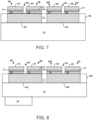
- the photoresist material layer 90 is then removed to provide the resultant structure of FIG. 7 that includes a first NIS junction 86, a second NIS junction 88, a third NIS junction 90a, and a fourth NIS junction 92.
- the first NIS junction 86 is formed of the first normal metal pad 62, a first aluminum layer 70, a first aluminum oxide layer 71, and a first superconductor pad 79.
- the second NIS junction 88 is formed of the first normal metal pad 62, a second aluminum layer 72, a second aluminum oxide layer 73 and a second superconductor pad 81.
- the third NIS junction 90a is formed of the second normal metal pad 64, a third aluminum layer 74, a third aluminum oxide layer 75 and a third superconductor pad 83
- the fourth NIS junction 92 is formed of the second normal metal pad 64, a fourth aluminum layer 76, a fourth aluminum oxide layer 77 and a fourth superconductor pad 85.
- the first, second, third and fourth aluminum layers 70, 72, 74 and 76 are selected to have a thickness (e.g., about 9 micrometers) thin enough to inverse proximitize with the normal metal layers 62 and 64.
- the first, second, third and fourth aluminum layers 70, 72, 74 and 76 work in cooperation with the first and second conductive pads 62 and 64 to form the normal metal layer of respective NIS or NISN tunnel junctions.
- the first, second, third and fourth aluminum oxide layers 71, 73, 75 and 77 are selected to have a thickness (e.g., about 9 Angstroms) thick enough to provide an insulator for a NIS or NISN tunnel junction.
- the backside of the first substrate 60 is thinned down by grinding or a chemical mechanical polish.
- An optional temperature sensor 84 can be formed on the backside of the first substrate 60 by depositing a layer of ruthenium oxide, which is then covered by a patterned photoresist material, and etched to provide the resultant temperature sensor 84 that resides on a bottom side of the first substrate 60, as illustrate in FIG. 8 .
- FIG. 9 illustrates a second portion of a solid state cooler in its early stages of fabrication.
- a first conductive pad 108, a second conductive pad 110 and a third conductive pad 112 are disposed on a second substrate 100.
- the first conductive pad 108, the second conductive pad 110 and the third conductive pad 112 can be formed by depositing and patterning a photoresist material, performing a metal evaporation process to deposit a normal metal (e.g., gold) and/or superconductor metal, and then performing a photoresist liftoff process (e.g., employing tape or solvent) to remove the photoresist and excess metal leaving the remaining metal in the form of the first conductive pad 108, the second conductive pad 110 and the third conductive pad 112, as illustrated in the structure of FIG. 9 .
- a photoresist liftoff process e.g., employing tape or solvent
- a photoresist material layer 114 is deposited and patterned with openings 115 over the structure of FIG. 9 to provide a bump layout (e.g., image reversal resist), as illustrated in FIG. 10 .
- an evaporation process is performed to evaporate a metal (e.g., gold) over the structure of FIG. 10 to provide the resultant structure of FIG. 11 .
- a liftoff process e.g., tape, or solvent
- the conductive contacts 118 can be either fabricated from a superconducting metal and/or a normal metal.
- the conductive contacts 118 can be formed through etching and deposition, as opposed to using a standard liftoff process as illustrated in FIGS. 10-12 .
- the conductive contacts can be formed on either the conductive pads as shown or on the superconductor pads.
- the second substrate 100 is then flipped and disposed over the first substrate 60 and bonded, such that the third conductive pad 112 is aligned and coupled to the first superconductor pad 79, a first end of the second conductive pad 110 is aligned and coupled to the second superconductor pad 81, a second end of the second conductive pad 110 is aligned and coupled to the third superconductor pad 83, and the first conductive pad 108 is aligned and coupled to the fourth superconductor pad 85.
- the resultant structure is illustrated in FIG. 13 .
- FIG. 14 illustrates a block diagram of a refrigeration system 250 that employs solid state devices such as the solid state device 10 of FIG. 1 .
- the refrigeration system 250 includes a plurality of stages labeled stage #1 to stage #N, where N is an integer greater than or equal to 2. Each refrigeration stage provides an additional temperature drop from the previous stage, such that the Nth stage is the final stage and provides the last temperature drop and lowest temperature of the refrigeration system 250. In other examples, the Nth stage is a first or intermediary stage as opposed to the last stage.
- Stage #N in the refrigeration system 250 includes a refrigeration container 260 with a plurality of solid state devices 270 simlar to that illustrated in FIG. 1 disposed about the container and cooperating to provide the final lowest temperature of the refrigeration system 250 within the container 260.
- the container 260 can be in a vacuum environment and be configured to house superconducting circuitry.
- one or more of the other stages employ solid state devices similar to those in stage #N to provide incremental temperature drops across the refrigeration system 250.
- the refrigeration container 260 can be formed of a normal metal that provides the final normal metal layer of each solid state device 270.
- overlay For purposes of simplification of explanation the terms “overlay”, “overlaying”, “overlying”, “underlay” and “underlying” (and derivatives) are employed throughout this disclosure to denote a relative position of two adjacent surfaces in a selected orientation. Additionally, the terms “top” and “bottom” employed throughout this disclosure denote opposing surfaces in the selected orientation. Similarly, the terms “upper” and “lower” denote relative positions in the selected orientation are for purposes of illustration. In fact, the examples used throughout this disclosure denote one selected orientation. In the described examples, however, the selected orientation is arbitrary and other orientations are possible (e.g., upside down, rotated by 90 degrees, etc.) within the scope of the present disclosure.
Landscapes
- Engineering & Computer Science (AREA)
- Physics & Mathematics (AREA)
- Mechanical Engineering (AREA)
- Thermal Sciences (AREA)
- General Engineering & Computer Science (AREA)
- Manufacturing & Machinery (AREA)
- Superconductor Devices And Manufacturing Methods Thereof (AREA)
- Containers, Films, And Cooling For Superconductive Devices (AREA)
Claims (14)
- Festkörper-Kühlervorrichtung (10), die Folgendes umfasst:ein erstes normales Metallpad (14);eine erste Aluminiumschicht (26) und eine zweite Aluminiumschicht (27), die auf dem ersten normalen Metallpad (14) angeordnet und voneinander durch einen ersten Spalt (49) getrennt sind;eine erste Aluminiumoxidschicht (28), die auf der ersten Aluminiumschicht (26) gebildet ist;und eine zweite Aluminiumoxidschicht (29), die auf der zweiten Aluminiumschicht (27) gebildet ist;ein erstes Supraleiterpad (30), das auf der ersten Aluminiumoxidschicht (28) angeordnet ist, und ein zweites Supraleiterpad (31), das auf der zweiten Aluminiumoxidschicht (29) angeordnet ist;ein erstes leitendes Pad (34), das mit dem ersten Supraleiterpad (30) gekoppelt ist, und ein zweites leitendes Pad (36), das mit dem zweiten Supraleiterpad (31) gekoppelt ist; undwobei heiße Elektronen von dem ersten normalen Metallpad (14) entfernt werden, wenn eine Vorspannung zwischen dem ersten leitenden Pad (34) und dem zweiten leitenden Pad (36) angelegt wird.
- Festkörper-Kühlervorrichtung (10) nach Anspruch 1, wobei jedes des ersten leitenden Pads (34) und des zweiten leitenden Pads (36) aus einem normalen Metall gebildet ist und als Quasiteilchen-Fallen fungiert.
- Festkörper-Kühlervorrichtung (10) nach Anspruch 1, wobei die erste (26) und die zweite (27) Aluminiumschicht eine Dicke aufweisen, die die erste (26) und die zweite (27) Aluminiumschicht veranlasst, auf dem ersten normalen Metallpad (14) invers zu proximitieren, und die erste (28) und die zweite (29) Aluminiumoxidschicht eine Dicke aufweisen, die ihre Funktionalität als ein Isolator sicherstellt.
- Festkörper-Kühlervorrichtung (10) nach Anspruch 1, wobei das erste normale Metallpad (14) auf oder in einem ersten Substrat (12) oder einer dielektrischen Schicht (13) angeordnet ist, und das erste (34) und das zweite (36) leitende Pad auf oder in einem zweiten Substrat (32) angeordnet sind, und wobei das erste leitende Pad (34) mit dem ersten Supraleiterpad (30) durch einen ersten Satz leitender Kontakte (40) gekoppelt ist, und das zweite leitende Pad (36) mit dem zweiten Supraleiterpad (31) durch einen zweiten Satz leitender Kontakte (40) gekoppelt ist.
- Festkörper-Kühlervorrichtung (10) nach Anspruch 1, wobei der erste und der zweite Satz leitender Kontakte (40) Höckerverbindungen derart sind, dass die Höckerverbindungen das erste Substrat (12) mit dem zweiten Substrat (32) verbinden.
- Festkörper-Kühlervorrichtung (10) nach Anspruch 1, wobei ein Temperatursensor (50) an einer Seite des ersten Substrats (12), der Seite des ersten normalen Metallpads (14) entgegengesetzt, angeordnet ist.
- Festkörper-Kühlervorrichtung (10) nach Anspruch 1, die ferner Folgendes umfasst:ein zweites normales Metallpad (16), wobei das erste normale Metallpad (14) und das zweite normale Metallpad (16) auf oder in einem ersten Substrat (12) oder einer dielektrischen Schicht (13) angeordnet und voneinander durch einen zweiten Spalt (15) getrennt sind;eine dritte Aluminiumschicht (33) und eine vierte Aluminiumschicht (39), die auf dem zweiten normalen Metallpad (16) angeordnet und voneinander durch einen dritten Spalt (51) getrennt sind;eine dritte Aluminiumoxidschicht (35), die auf der dritten Aluminiumschicht (33) gebildet ist, und eine vierte Aluminiumoxidschicht (41), die auf der vierten Aluminiumschicht (39) gebildet ist;ein drittes Supraleiterpad (37), das auf der dritten Aluminiumoxidschicht (35) angeordnet ist, und ein viertes Supraleiterpad (43), das auf der vierten Aluminiumoxidschicht (41) angeordnet ist, wobei ein erstes Ende des zweiten leitenden Pads (36) mit dem zweiten Supraleiterpad (31) gekoppelt ist, und ein zweites Ende des zweiten leitenden Pads (36) mit dem dritten Supraleiterpad (37) gekoppelt ist; undein drittes leitendes Pad (38) mit dem vierten Supraleiterpad (43) gekoppelt ist.
- Festkörper-Kühlervorrichtung (10) nach Anspruch 7, die ferner einen ersten Stromdraht (44) umfasst, der mit dem ersten leitenden Pad (34) gekoppelt ist, und einen zweiten Stromdraht (48), der mit dem dritten leitenden Pad (38) gekoppelt ist, wobei heiße Elektronen von dem ersten normalen Metallpad (14) und dem zweiten normalen Metallpad (16) entfernt werden, wenn die Vorspannung zwischen dem ersten Stromdraht (44) und dem zweiten Stromdraht (48) angelegt wird.
- Kühlsystem (250), das eine Vielzahl von Kühlstufen (#1, ..., #N) umfasst, wobei eine letzte Stufe einen Kühlbehälter (260) und eine Vielzahl von Festkörper-Kühlervorrichtungen (270, 10) nach Anspruch 1, die um den Kühlbehälter (260) angeordnet ist, umfasst.
- Verfahren zum Herstellen einer Festkörper-Kühlervorrichtung, wobei das Verfahren Folgendes umfasst:Bilden eines ersten normalen Metallpads (62) auf oder in einem ersten Substrat (60) oder auf oder in einer dielektrischen Schicht (66), die dem ersten Substrat (60) überlagert ist;Bilden einer Aluminiumschicht (67) über dem ersten normalen Metallpad (62);Durchführen eines Oxidationsprozesses an der Aluminiumschicht (67), um eine Aluminiumoxidschicht (68), die der Aluminiumschicht (67) überlagert ist, zu bilden;Bilden einer Supraleiterschicht (69) über der Aluminiumoxidschicht (68);Bilden einer strukturierten Maske (90) über der Supraleiterschicht (69);Durchführen eines Ätzprozesses, um Teile der Supraleiterschicht (69), der Aluminiumoxidschicht (68) und der Aluminiumschicht (67) basierend auf der strukturierten Maske zu entfernen, um einen ersten normalen Metall-Isolator-Supraleiter-Übergang, NIS-Übergang (86), der das erste normale Metallpad (62) einschließt, eine erste Aluminiumschicht (70), eine erste Aluminiumoxidschicht (71), die der ersten Aluminiumschicht (70) überlagert ist, und ein erstes Supraleiterpad (79), das der ersten Aluminiumschicht (71) überlagert ist, und einen zweiten NIS-Übergang (88), der das erste normale Metallpad (62), eine zweite Aluminiumschicht (72), eine zweite Aluminiumoxidschicht (73), die der zweiten Aluminiumschicht (72) überlagert ist, und ein zweites Supraleiterpad (81), das der zweiten Aluminiumoxidschicht (73) überlagert ist, einschließt, zu bilden, wobei der erste und der zweite NIS-Übergang (86, 88) voneinander durch einen ersten Spalt (78) getrennt sind,Bilden eines ersten leitenden Pads (108) und eines zweiten leitenden Pads (110) in oder auf einem zweiten Substrat (100), und Koppeln des ersten leitenden Pads (108) mit dem ersten Supraleiterpad (79), und Koppeln des zweiten leitenden Pads (110) mit dem zweiten Supraleiterpad (81),wobei heiße Elektronen von dem ersten normalen Metallpad (62) entfernt werden, wenn eine Vorspannung zwischen dem ersten leitenden Pad (108) und dem zweiten leitenden Pad (110) angelegt wird.
- Verfahren nach Anspruch 10, das ferner Folgendes umfasst:Bilden eines ersten Satzes leitender Kontakte (118) an einem des ersten Supraleiterpads (79) und des ersten leitenden Pads (108);Bilden eines zweiten Satzes leitender Kontakte (118) auf einem des zweiten Supraleiterpads (81) und des zweiten leitenden Pads (110); undKoppeln des ersten Supraleiterpads (79) mit dem ersten leitenden Pad (108) über den ersten Satz leitender Kontakte (118), und Koppeln des zweiten Supraleiterpads (81) mit dem zweiten leitenden Pad (110) über den zweiten Satz leitender Kontakte (118),wobei der erste und der zweite Satz leitender Kontakte (118) Höckerverbindungen derart sind, dass die Höckerverbindungen das erste Substrat (60) mit dem zweiten Substrat (100) verbinden.
- Verfahren nach Anspruch 10, das ferner das Verdünnen einer zweiten Seite des ersten Substrats (60), der Seite des ersten normalen Metallpads (62) entgegengesetzt, und das Fertigen eines Temperatursensors (84) an der zweiten Seite umfasst.
- Verfahren nach Anspruch 10, das weiter Folgendes umfasst:Bilden eines zweiten normalen Metallpads (64) auf oder in dem ersten Substrat (60) oder auf oder in der dielektrischen Schicht (66), die dem ersten Substrat (60) überlagert ist;wobei das Bilden die Aluminiumschicht (67) über dem ersten normalen Metallpad ferner das Bilden der Aluminiumschicht (67) über dem zweiten normalen Metallpad (110) umfasst;wobei das Durchführen eines Ätzprozesses, um Teile der Supraleiterschicht (69), der Aluminiumoxidschicht (68) und der Aluminiumschicht (67) basierend auf der strukturierten Maske (90) zu entfernen, auch einen dritten NIS-Übergang (90a), der das zweite normale Metallpad (64) einschließt, eine dritte Aluminiumschicht (74), eine dritte Aluminiumoxidschicht (75), die der dritten Aluminiumschicht (74) überlagert ist, und ein drittes Supraleiterpad (83), das der dritten Aluminiumoxidschicht (75) überlagert ist, und einen vierten NIS-Übergang (92), der das zweite normale Metallpad (64) einschließt, eine vierte Aluminiumschicht (76), eine vierte Aluminiumoxidschicht (77), die der vierten Aluminiumschicht (76) überlagert ist, und ein viertes Supraleiterpad (85), das der vierten Aluminiumschicht (77) überlagert ist, bildet, wobei der dritte NIS-Übergang (90a) von dem zweiten NIS-Übergang (88) durch eine zweite Spalte (78) getrennt ist, und der dritte NIS-Übergang (90a) von dem vierten NIS-Übergang (92) durch einen dritten Spalt (82) getrennt ist;Koppeln des zweiten leitenden Pads (110) mit dem dritten Supraleiterpad (83), wobei ein erstes Ende des zweiten leitenden Pads (110) mit dem zweiten Supraleiterpad (81) gekoppelt ist, und ein zweites Ende des zweiten leitenden Pads (110) mit dem dritten Supraleiterpad (83) gekoppelt ist; undKoppeln eines dritten leitenden Pads (112) mit dem vierten Supraleiterpad (85).
- Verfahren nach Anspruch 13, das ferner das Koppeln eines ersten Drahtes mit dem ersten leitenden Pad (108) und das Koppeln eines zweiten Drahtes mit dem dritten leitenden Pad (112) umfasst, wobei heiße Elektronen von dem ersten normalen Metallpad (62) und dem zweiten normalen Metallpad (64) entfernt werden, wenn eine Vorspannung zwischen dem ersten Draht und dem zweiten Draht angelegt wird.
Applications Claiming Priority (2)
| Application Number | Priority Date | Filing Date | Title |
|---|---|---|---|
| US16/696,372 US11600760B2 (en) | 2019-11-26 | 2019-11-26 | Cooler device with aluminum oxide insulators |
| PCT/US2020/053789 WO2021108032A1 (en) | 2019-11-26 | 2020-10-01 | Cooler device with aluminum oxide insulators |
Publications (2)
| Publication Number | Publication Date |
|---|---|
| EP4066286A1 EP4066286A1 (de) | 2022-10-05 |
| EP4066286B1 true EP4066286B1 (de) | 2023-12-27 |
Family
ID=72964826
Family Applications (1)
| Application Number | Title | Priority Date | Filing Date |
|---|---|---|---|
| EP20793891.1A Active EP4066286B1 (de) | 2019-11-26 | 2020-10-01 | Kühlervorrichtung mit aluminiumoxidisolatoren |
Country Status (4)
| Country | Link |
|---|---|
| US (2) | US11600760B2 (de) |
| EP (1) | EP4066286B1 (de) |
| JP (1) | JP7358640B2 (de) |
| WO (1) | WO2021108032A1 (de) |
Families Citing this family (5)
| Publication number | Priority date | Publication date | Assignee | Title |
|---|---|---|---|---|
| US10998485B1 (en) * | 2020-01-13 | 2021-05-04 | Northrop Grumman Systems Corporation | Cooler device with superconductor shunts |
| JP2024530270A (ja) * | 2021-08-23 | 2024-08-16 | テクノロギアン トゥトキムスケスクス ヴェーテーテー オイ | アッテネータ又は放散要素 |
| US11950510B2 (en) * | 2022-02-03 | 2024-04-02 | Northrop Grumman Systems Corporation | Superconductor junction for a solid state cooler |
| US20260036345A1 (en) * | 2023-08-01 | 2026-02-05 | Northrop Grumman Systems Corporation | Solid-State Cooler Device with Normal Metal Substrates |
| US12426504B2 (en) * | 2023-08-01 | 2025-09-23 | Northrop Grumman Systems Corporation | Solid-state cooler device with grid point contacts |
Family Cites Families (29)
| Publication number | Priority date | Publication date | Assignee | Title |
|---|---|---|---|---|
| US4837604A (en) * | 1986-04-18 | 1989-06-06 | Hypres, Inc. | Femtosecond three-terminal switch and vertical tunnel junction |
| US5237821A (en) * | 1987-08-20 | 1993-08-24 | Kabushiki Kaisha Komatsu Seisakusho | Multistep electronic cooler |
| JP2636119B2 (ja) * | 1992-09-08 | 1997-07-30 | 工業技術院長 | 熱電素子シートとその製造方法 |
| US5385022A (en) * | 1993-09-09 | 1995-01-31 | Kornblit; Levy | Apparatus and method for deep thermoelectric refrigeration |
| JP3980682B2 (ja) | 1996-07-22 | 2007-09-26 | 三洋電機株式会社 | 酸化物超電導デバイスの形成方法 |
| US6505468B2 (en) * | 2000-03-21 | 2003-01-14 | Research Triangle Institute | Cascade cryogenic thermoelectric cooler for cryogenic and room temperature applications |
| JP2002111083A (ja) * | 2000-09-29 | 2002-04-12 | Aisin Seiki Co Ltd | 熱電モジュール及びその製造方法 |
| US7942010B2 (en) * | 2001-02-09 | 2011-05-17 | Bsst, Llc | Thermoelectric power generating systems utilizing segmented thermoelectric elements |
| US6581387B1 (en) * | 2001-02-12 | 2003-06-24 | The United States Of America As Represented By The United States Department Of Energy | Solid-state microrefrigerator |
| US6779347B2 (en) * | 2001-05-21 | 2004-08-24 | C.P. Baker Securities, Inc. | Solid-state thermionic refrigeration |
| US6557354B1 (en) * | 2002-04-04 | 2003-05-06 | International Business Machines Corporation | Thermoelectric-enhanced heat exchanger |
| TWI252920B (en) * | 2005-03-25 | 2006-04-11 | Ind Tech Res Inst | Method of fabricating an integral device of a biochip integrated with micro thermo-electric elements and the apparatus thereof |
| EP2302710B1 (de) * | 2008-11-29 | 2013-01-16 | Alstom Technology Ltd. | Fehlerstrombegrenzer mit mehreren supraleitenden Elementen mit mindestens einem Element mit einem elektrischen Kontakt zwischen dessen supraleitender Schicht und dessen elektrisch leitfähigem Substrat |
| WO2011083462A2 (en) * | 2010-01-06 | 2011-07-14 | Novatrans Group Sa | Thermo-electric cooling system and method for cooling electronic devices |
| US8301214B1 (en) | 2010-01-08 | 2012-10-30 | Hypres, Inc. | System and method for providing multi-conductive layer metallic interconnects for superconducting integrated circuits |
| KR20110119334A (ko) * | 2010-04-27 | 2011-11-02 | 삼성전기주식회사 | 열전 모듈 및 이의 제조방법 |
| KR101928005B1 (ko) * | 2011-12-01 | 2019-03-13 | 삼성전자주식회사 | 열전 냉각 패키지 및 이의 열관리 방법 |
| US9082927B1 (en) * | 2013-12-20 | 2015-07-14 | Intermolecular, Inc. | Catalytic growth of Josephson junction tunnel barrier |
| KR102281065B1 (ko) * | 2014-01-23 | 2021-07-23 | 엘지이노텍 주식회사 | 열전모듈 및 이를 포함하는 냉각장치 |
| DE102014222706B4 (de) * | 2014-11-06 | 2018-05-03 | Dialog Semiconductor B.V. | Thermoelektrische Vorrichtung auf einem Chip |
| FI20165492A (fi) | 2015-12-29 | 2017-06-30 | Aalto-Korkeakoulusäätiö (Aalto Univ Foundation) | Piirikokoonpano, järjestelmä ja menetelmä sähköisten kvanttilaitteiden jäähdyttämiseksi |
| KR102274676B1 (ko) * | 2017-03-14 | 2021-07-08 | 엘지전자 주식회사 | 냉장고 |
| US10243132B1 (en) * | 2018-03-23 | 2019-03-26 | International Business Machines Corporation | Vertical josephson junction superconducting device |
| US20190371992A1 (en) * | 2018-05-29 | 2019-12-05 | Faurecia Automotive Seating, Llc | High resistance thermoelectric element |
| US20200217565A1 (en) * | 2019-01-04 | 2020-07-09 | Matrix Industries, Inc. | Thermoelectric cooling devices, systems and methods |
| US10840295B2 (en) * | 2019-04-17 | 2020-11-17 | International Business Machines Corporation | Fluxonium qubits and devices including plurality of vertical stacks of Josephson junctions |
| US11189773B2 (en) | 2019-08-28 | 2021-11-30 | Northrop Grumman Systems Corporation | Superconductor thermal filter |
| US11333413B2 (en) | 2019-08-28 | 2022-05-17 | Northrop Grumman Systems Corporation | Solid state cooler device |
| US10998485B1 (en) * | 2020-01-13 | 2021-05-04 | Northrop Grumman Systems Corporation | Cooler device with superconductor shunts |
-
2019
- 2019-11-26 US US16/696,372 patent/US11600760B2/en active Active
-
2020
- 2020-10-01 JP JP2022525121A patent/JP7358640B2/ja active Active
- 2020-10-01 WO PCT/US2020/053789 patent/WO2021108032A1/en not_active Ceased
- 2020-10-01 EP EP20793891.1A patent/EP4066286B1/de active Active
-
2023
- 2023-02-01 US US18/163,203 patent/US11839165B2/en active Active
Also Published As
| Publication number | Publication date |
|---|---|
| WO2021108032A1 (en) | 2021-06-03 |
| US11600760B2 (en) | 2023-03-07 |
| US20230180634A1 (en) | 2023-06-08 |
| US20210257533A1 (en) | 2021-08-19 |
| EP4066286A1 (de) | 2022-10-05 |
| US11839165B2 (en) | 2023-12-05 |
| JP2023500487A (ja) | 2023-01-06 |
| JP7358640B2 (ja) | 2023-10-10 |
Similar Documents
| Publication | Publication Date | Title |
|---|---|---|
| US11839165B2 (en) | Cooler device with aluminum oxide insulators | |
| EP4091205B1 (de) | Kühlvorrichtung mit supraleitenden shunts und herstellungsverfahren einer kühlvorrichtung | |
| EP4022690B1 (de) | Supraleitender thermischer filter | |
| EP4022691B1 (de) | Festkörperkühler | |
| US10134972B2 (en) | Qubit and coupler circuit structures and coupling techniques | |
| US10170679B2 (en) | Josephson junction with spacer | |
| JP2007518281A (ja) | 補助的熱伝物質を含む一体化薄膜熱電装置 | |
| US12588166B2 (en) | Thermalization arrangement at cryogenic temperatures | |
| CN114256357A (zh) | 具有双功能布线的芯片和相关的制造方法 | |
| CN114256358A (zh) | 具有双功能布线的集成结构和包括这种结构的组件 | |
| US20230017631A1 (en) | Electronic device intended to connect a first electronic component to a second electronic component, system comprising such a device and methods making it possible to obtain such a device | |
| US20260036345A1 (en) | Solid-State Cooler Device with Normal Metal Substrates | |
| US12426504B2 (en) | Solid-state cooler device with grid point contacts | |
| US11950510B2 (en) | Superconductor junction for a solid state cooler | |
| US20050092981A1 (en) | Superconducting integrated circuit and methods of forming same | |
| JPS61201467A (ja) | 超電導トランジスタ集積回路 | |
| JPH01175246A (ja) | 半導体装置 | |
| JPH0758368A (ja) | 超伝導物質を用いた電子回路素子 |
Legal Events
| Date | Code | Title | Description |
|---|---|---|---|
| STAA | Information on the status of an ep patent application or granted ep patent |
Free format text: STATUS: UNKNOWN |
|
| STAA | Information on the status of an ep patent application or granted ep patent |
Free format text: STATUS: THE INTERNATIONAL PUBLICATION HAS BEEN MADE |
|
| PUAI | Public reference made under article 153(3) epc to a published international application that has entered the european phase |
Free format text: ORIGINAL CODE: 0009012 |
|
| STAA | Information on the status of an ep patent application or granted ep patent |
Free format text: STATUS: REQUEST FOR EXAMINATION WAS MADE |
|
| 17P | Request for examination filed |
Effective date: 20220413 |
|
| AK | Designated contracting states |
Kind code of ref document: A1 Designated state(s): AL AT BE BG CH CY CZ DE DK EE ES FI FR GB GR HR HU IE IS IT LI LT LU LV MC MK MT NL NO PL PT RO RS SE SI SK SM TR |
|
| DAV | Request for validation of the european patent (deleted) | ||
| DAX | Request for extension of the european patent (deleted) | ||
| REG | Reference to a national code |
Ref country code: DE Ref legal event code: R079 Free format text: PREVIOUS MAIN CLASS: H01L0039220000 Ipc: H10N0060100000 Ref document number: 602020023497 Country of ref document: DE |
|
| RIC1 | Information provided on ipc code assigned before grant |
Ipc: F25B 21/00 20060101ALI20230421BHEP Ipc: H10N 60/01 20230101ALI20230421BHEP Ipc: H10N 60/10 20230101AFI20230421BHEP |
|
| GRAP | Despatch of communication of intention to grant a patent |
Free format text: ORIGINAL CODE: EPIDOSNIGR1 |
|
| STAA | Information on the status of an ep patent application or granted ep patent |
Free format text: STATUS: GRANT OF PATENT IS INTENDED |
|
| P01 | Opt-out of the competence of the unified patent court (upc) registered |
Effective date: 20230607 |
|
| INTG | Intention to grant announced |
Effective date: 20230705 |
|
| GRAS | Grant fee paid |
Free format text: ORIGINAL CODE: EPIDOSNIGR3 |
|
| GRAA | (expected) grant |
Free format text: ORIGINAL CODE: 0009210 |
|
| STAA | Information on the status of an ep patent application or granted ep patent |
Free format text: STATUS: THE PATENT HAS BEEN GRANTED |
|
| AK | Designated contracting states |
Kind code of ref document: B1 Designated state(s): AL AT BE BG CH CY CZ DE DK EE ES FI FR GB GR HR HU IE IS IT LI LT LU LV MC MK MT NL NO PL PT RO RS SE SI SK SM TR |
|
| REG | Reference to a national code |
Ref country code: GB Ref legal event code: FG4D |
|
| REG | Reference to a national code |
Ref country code: CH Ref legal event code: EP |
|
| REG | Reference to a national code |
Ref country code: DE Ref legal event code: R096 Ref document number: 602020023497 Country of ref document: DE |
|
| REG | Reference to a national code |
Ref country code: IE Ref legal event code: FG4D |
|
| REG | Reference to a national code |
Ref country code: NL Ref legal event code: FP |
|
| PG25 | Lapsed in a contracting state [announced via postgrant information from national office to epo] |
Ref country code: GR Free format text: LAPSE BECAUSE OF FAILURE TO SUBMIT A TRANSLATION OF THE DESCRIPTION OR TO PAY THE FEE WITHIN THE PRESCRIBED TIME-LIMIT Effective date: 20240328 |
|
| REG | Reference to a national code |
Ref country code: LT Ref legal event code: MG9D |
|
| PG25 | Lapsed in a contracting state [announced via postgrant information from national office to epo] |
Ref country code: LT Free format text: LAPSE BECAUSE OF FAILURE TO SUBMIT A TRANSLATION OF THE DESCRIPTION OR TO PAY THE FEE WITHIN THE PRESCRIBED TIME-LIMIT Effective date: 20231227 |
|
| PG25 | Lapsed in a contracting state [announced via postgrant information from national office to epo] |
Ref country code: ES Free format text: LAPSE BECAUSE OF FAILURE TO SUBMIT A TRANSLATION OF THE DESCRIPTION OR TO PAY THE FEE WITHIN THE PRESCRIBED TIME-LIMIT Effective date: 20231227 |
|
| PG25 | Lapsed in a contracting state [announced via postgrant information from national office to epo] |
Ref country code: LT Free format text: LAPSE BECAUSE OF FAILURE TO SUBMIT A TRANSLATION OF THE DESCRIPTION OR TO PAY THE FEE WITHIN THE PRESCRIBED TIME-LIMIT Effective date: 20231227 Ref country code: GR Free format text: LAPSE BECAUSE OF FAILURE TO SUBMIT A TRANSLATION OF THE DESCRIPTION OR TO PAY THE FEE WITHIN THE PRESCRIBED TIME-LIMIT Effective date: 20240328 Ref country code: FI Free format text: LAPSE BECAUSE OF FAILURE TO SUBMIT A TRANSLATION OF THE DESCRIPTION OR TO PAY THE FEE WITHIN THE PRESCRIBED TIME-LIMIT Effective date: 20231227 Ref country code: ES Free format text: LAPSE BECAUSE OF FAILURE TO SUBMIT A TRANSLATION OF THE DESCRIPTION OR TO PAY THE FEE WITHIN THE PRESCRIBED TIME-LIMIT Effective date: 20231227 Ref country code: BG Free format text: LAPSE BECAUSE OF FAILURE TO SUBMIT A TRANSLATION OF THE DESCRIPTION OR TO PAY THE FEE WITHIN THE PRESCRIBED TIME-LIMIT Effective date: 20240327 |
|
| REG | Reference to a national code |
Ref country code: AT Ref legal event code: MK05 Ref document number: 1645788 Country of ref document: AT Kind code of ref document: T Effective date: 20231227 |
|
| PG25 | Lapsed in a contracting state [announced via postgrant information from national office to epo] |
Ref country code: SE Free format text: LAPSE BECAUSE OF FAILURE TO SUBMIT A TRANSLATION OF THE DESCRIPTION OR TO PAY THE FEE WITHIN THE PRESCRIBED TIME-LIMIT Effective date: 20231227 Ref country code: RS Free format text: LAPSE BECAUSE OF FAILURE TO SUBMIT A TRANSLATION OF THE DESCRIPTION OR TO PAY THE FEE WITHIN THE PRESCRIBED TIME-LIMIT Effective date: 20231227 Ref country code: NO Free format text: LAPSE BECAUSE OF FAILURE TO SUBMIT A TRANSLATION OF THE DESCRIPTION OR TO PAY THE FEE WITHIN THE PRESCRIBED TIME-LIMIT Effective date: 20240327 Ref country code: LV Free format text: LAPSE BECAUSE OF FAILURE TO SUBMIT A TRANSLATION OF THE DESCRIPTION OR TO PAY THE FEE WITHIN THE PRESCRIBED TIME-LIMIT Effective date: 20231227 Ref country code: HR Free format text: LAPSE BECAUSE OF FAILURE TO SUBMIT A TRANSLATION OF THE DESCRIPTION OR TO PAY THE FEE WITHIN THE PRESCRIBED TIME-LIMIT Effective date: 20231227 |
|
| PG25 | Lapsed in a contracting state [announced via postgrant information from national office to epo] |
Ref country code: IS Free format text: LAPSE BECAUSE OF FAILURE TO SUBMIT A TRANSLATION OF THE DESCRIPTION OR TO PAY THE FEE WITHIN THE PRESCRIBED TIME-LIMIT Effective date: 20240427 |
|
| PG25 | Lapsed in a contracting state [announced via postgrant information from national office to epo] |
Ref country code: CZ Free format text: LAPSE BECAUSE OF FAILURE TO SUBMIT A TRANSLATION OF THE DESCRIPTION OR TO PAY THE FEE WITHIN THE PRESCRIBED TIME-LIMIT Effective date: 20231227 Ref country code: AT Free format text: LAPSE BECAUSE OF FAILURE TO SUBMIT A TRANSLATION OF THE DESCRIPTION OR TO PAY THE FEE WITHIN THE PRESCRIBED TIME-LIMIT Effective date: 20231227 |
|
| PG25 | Lapsed in a contracting state [announced via postgrant information from national office to epo] |
Ref country code: SK Free format text: LAPSE BECAUSE OF FAILURE TO SUBMIT A TRANSLATION OF THE DESCRIPTION OR TO PAY THE FEE WITHIN THE PRESCRIBED TIME-LIMIT Effective date: 20231227 |
|
| PG25 | Lapsed in a contracting state [announced via postgrant information from national office to epo] |
Ref country code: SM Free format text: LAPSE BECAUSE OF FAILURE TO SUBMIT A TRANSLATION OF THE DESCRIPTION OR TO PAY THE FEE WITHIN THE PRESCRIBED TIME-LIMIT Effective date: 20231227 Ref country code: SK Free format text: LAPSE BECAUSE OF FAILURE TO SUBMIT A TRANSLATION OF THE DESCRIPTION OR TO PAY THE FEE WITHIN THE PRESCRIBED TIME-LIMIT Effective date: 20231227 Ref country code: RO Free format text: LAPSE BECAUSE OF FAILURE TO SUBMIT A TRANSLATION OF THE DESCRIPTION OR TO PAY THE FEE WITHIN THE PRESCRIBED TIME-LIMIT Effective date: 20231227 Ref country code: IT Free format text: LAPSE BECAUSE OF FAILURE TO SUBMIT A TRANSLATION OF THE DESCRIPTION OR TO PAY THE FEE WITHIN THE PRESCRIBED TIME-LIMIT Effective date: 20231227 Ref country code: IS Free format text: LAPSE BECAUSE OF FAILURE TO SUBMIT A TRANSLATION OF THE DESCRIPTION OR TO PAY THE FEE WITHIN THE PRESCRIBED TIME-LIMIT Effective date: 20240427 Ref country code: EE Free format text: LAPSE BECAUSE OF FAILURE TO SUBMIT A TRANSLATION OF THE DESCRIPTION OR TO PAY THE FEE WITHIN THE PRESCRIBED TIME-LIMIT Effective date: 20231227 Ref country code: CZ Free format text: LAPSE BECAUSE OF FAILURE TO SUBMIT A TRANSLATION OF THE DESCRIPTION OR TO PAY THE FEE WITHIN THE PRESCRIBED TIME-LIMIT Effective date: 20231227 Ref country code: AT Free format text: LAPSE BECAUSE OF FAILURE TO SUBMIT A TRANSLATION OF THE DESCRIPTION OR TO PAY THE FEE WITHIN THE PRESCRIBED TIME-LIMIT Effective date: 20231227 |
|
| PG25 | Lapsed in a contracting state [announced via postgrant information from national office to epo] |
Ref country code: PL Free format text: LAPSE BECAUSE OF FAILURE TO SUBMIT A TRANSLATION OF THE DESCRIPTION OR TO PAY THE FEE WITHIN THE PRESCRIBED TIME-LIMIT Effective date: 20231227 Ref country code: PT Free format text: LAPSE BECAUSE OF FAILURE TO SUBMIT A TRANSLATION OF THE DESCRIPTION OR TO PAY THE FEE WITHIN THE PRESCRIBED TIME-LIMIT Effective date: 20240429 |
|
| PG25 | Lapsed in a contracting state [announced via postgrant information from national office to epo] |
Ref country code: PT Free format text: LAPSE BECAUSE OF FAILURE TO SUBMIT A TRANSLATION OF THE DESCRIPTION OR TO PAY THE FEE WITHIN THE PRESCRIBED TIME-LIMIT Effective date: 20240429 Ref country code: PL Free format text: LAPSE BECAUSE OF FAILURE TO SUBMIT A TRANSLATION OF THE DESCRIPTION OR TO PAY THE FEE WITHIN THE PRESCRIBED TIME-LIMIT Effective date: 20231227 |
|
| REG | Reference to a national code |
Ref country code: DE Ref legal event code: R097 Ref document number: 602020023497 Country of ref document: DE |
|
| PG25 | Lapsed in a contracting state [announced via postgrant information from national office to epo] |
Ref country code: DK Free format text: LAPSE BECAUSE OF FAILURE TO SUBMIT A TRANSLATION OF THE DESCRIPTION OR TO PAY THE FEE WITHIN THE PRESCRIBED TIME-LIMIT Effective date: 20231227 |
|
| PG25 | Lapsed in a contracting state [announced via postgrant information from national office to epo] |
Ref country code: DK Free format text: LAPSE BECAUSE OF FAILURE TO SUBMIT A TRANSLATION OF THE DESCRIPTION OR TO PAY THE FEE WITHIN THE PRESCRIBED TIME-LIMIT Effective date: 20231227 |
|
| PLBE | No opposition filed within time limit |
Free format text: ORIGINAL CODE: 0009261 |
|
| STAA | Information on the status of an ep patent application or granted ep patent |
Free format text: STATUS: NO OPPOSITION FILED WITHIN TIME LIMIT |
|
| 26N | No opposition filed |
Effective date: 20240930 |
|
| PG25 | Lapsed in a contracting state [announced via postgrant information from national office to epo] |
Ref country code: SI Free format text: LAPSE BECAUSE OF FAILURE TO SUBMIT A TRANSLATION OF THE DESCRIPTION OR TO PAY THE FEE WITHIN THE PRESCRIBED TIME-LIMIT Effective date: 20231227 |
|
| REG | Reference to a national code |
Ref country code: CH Ref legal event code: PL |
|
| PG25 | Lapsed in a contracting state [announced via postgrant information from national office to epo] |
Ref country code: MC Free format text: LAPSE BECAUSE OF FAILURE TO SUBMIT A TRANSLATION OF THE DESCRIPTION OR TO PAY THE FEE WITHIN THE PRESCRIBED TIME-LIMIT Effective date: 20231227 |
|
| PG25 | Lapsed in a contracting state [announced via postgrant information from national office to epo] |
Ref country code: LU Free format text: LAPSE BECAUSE OF NON-PAYMENT OF DUE FEES Effective date: 20241001 |
|
| PG25 | Lapsed in a contracting state [announced via postgrant information from national office to epo] |
Ref country code: FR Free format text: LAPSE BECAUSE OF NON-PAYMENT OF DUE FEES Effective date: 20241031 |
|
| PG25 | Lapsed in a contracting state [announced via postgrant information from national office to epo] |
Ref country code: CH Free format text: LAPSE BECAUSE OF NON-PAYMENT OF DUE FEES Effective date: 20241031 |
|
| PG25 | Lapsed in a contracting state [announced via postgrant information from national office to epo] |
Ref country code: IE Free format text: LAPSE BECAUSE OF NON-PAYMENT OF DUE FEES Effective date: 20241001 |
|
| PGFP | Annual fee paid to national office [announced via postgrant information from national office to epo] |
Ref country code: NL Payment date: 20251021 Year of fee payment: 6 |
|
| PGFP | Annual fee paid to national office [announced via postgrant information from national office to epo] |
Ref country code: DE Payment date: 20251021 Year of fee payment: 6 |
|
| PGFP | Annual fee paid to national office [announced via postgrant information from national office to epo] |
Ref country code: GB Payment date: 20251022 Year of fee payment: 6 |
|
| PGFP | Annual fee paid to national office [announced via postgrant information from national office to epo] |
Ref country code: BE Payment date: 20251021 Year of fee payment: 6 |
|
| PG25 | Lapsed in a contracting state [announced via postgrant information from national office to epo] |
Ref country code: CY Free format text: LAPSE BECAUSE OF FAILURE TO SUBMIT A TRANSLATION OF THE DESCRIPTION OR TO PAY THE FEE WITHIN THE PRESCRIBED TIME-LIMIT; INVALID AB INITIO Effective date: 20201001 |
|
| PG25 | Lapsed in a contracting state [announced via postgrant information from national office to epo] |
Ref country code: HU Free format text: LAPSE BECAUSE OF FAILURE TO SUBMIT A TRANSLATION OF THE DESCRIPTION OR TO PAY THE FEE WITHIN THE PRESCRIBED TIME-LIMIT; INVALID AB INITIO Effective date: 20201001 |