EP4063134B1 - Thermodruckkopf und thermodrucker - Google Patents
Thermodruckkopf und thermodrucker Download PDFInfo
- Publication number
- EP4063134B1 EP4063134B1 EP20891337.6A EP20891337A EP4063134B1 EP 4063134 B1 EP4063134 B1 EP 4063134B1 EP 20891337 A EP20891337 A EP 20891337A EP 4063134 B1 EP4063134 B1 EP 4063134B1
- Authority
- EP
- European Patent Office
- Prior art keywords
- substrate
- recessed portions
- thermal head
- wiring board
- generating unit
- Prior art date
- Legal status (The legal status is an assumption and is not a legal conclusion. Google has not performed a legal analysis and makes no representation as to the accuracy of the status listed.)
- Active
Links
Images


Classifications
-
- B—PERFORMING OPERATIONS; TRANSPORTING
- B41—PRINTING; LINING MACHINES; TYPEWRITERS; STAMPS
- B41J—TYPEWRITERS; SELECTIVE PRINTING MECHANISMS, i.e. MECHANISMS PRINTING OTHERWISE THAN FROM A FORME; CORRECTION OF TYPOGRAPHICAL ERRORS
- B41J2/00—Typewriters or selective printing mechanisms characterised by the printing or marking process for which they are designed
- B41J2/315—Typewriters or selective printing mechanisms characterised by the printing or marking process for which they are designed characterised by selective application of heat to a heat sensitive printing or impression-transfer material
- B41J2/32—Typewriters or selective printing mechanisms characterised by the printing or marking process for which they are designed characterised by selective application of heat to a heat sensitive printing or impression-transfer material using thermal heads
- B41J2/335—Structure of thermal heads
-
- B—PERFORMING OPERATIONS; TRANSPORTING
- B41—PRINTING; LINING MACHINES; TYPEWRITERS; STAMPS
- B41J—TYPEWRITERS; SELECTIVE PRINTING MECHANISMS, i.e. MECHANISMS PRINTING OTHERWISE THAN FROM A FORME; CORRECTION OF TYPOGRAPHICAL ERRORS
- B41J2/00—Typewriters or selective printing mechanisms characterised by the printing or marking process for which they are designed
- B41J2/315—Typewriters or selective printing mechanisms characterised by the printing or marking process for which they are designed characterised by selective application of heat to a heat sensitive printing or impression-transfer material
- B41J2/32—Typewriters or selective printing mechanisms characterised by the printing or marking process for which they are designed characterised by selective application of heat to a heat sensitive printing or impression-transfer material using thermal heads
- B41J2/345—Typewriters or selective printing mechanisms characterised by the printing or marking process for which they are designed characterised by selective application of heat to a heat sensitive printing or impression-transfer material using thermal heads characterised by the arrangement of resistors or conductors
Definitions
- Embodiments of the present disclosure relate to a thermal head and a thermal printer.
- thermal heads have been proposed as printing devices such as facsimile machines and video printers.
- a thermal head in which a head substrate and a wiring board being in contact with each other are connected by wires and sealed with an insulating resin member.
- an insulating resin member in order to reduce the generation of air bubbles at the time of curing the resin member, there is disclosed a structure in which portions other than both end portions on a contact side of the wiring board in contact with the head substrate are cut off (see Patent Document 1, for example).
- Patent Document 1 JP 06-17939 UM-A US 2014/022325 A1 discloses a thermal head including heat generating members, a drive IC, pads and interconnection lines which are all disposed on a substrate, wherein the pads are arranged in a first direction and constitute first pad groups and second pad groups constituted by the pads that constitute the first pad groups, and wherein the second pad groups are arranged in the first direction so as to be shifted from each other in a second direction that differs from the first direction.
- JP 2018 051973 A discloses a thermal print head including a drive circuit, a circuit board, a sealing material, and an air gap, wherein the drive circuit is provided on a first ceramic plate, wherein the circuit board is provided on a second ceramic plate, and wherein the sealing material is provided to cover the drive circuit, a part of the circuit board and the first ceramic plate, the thermal print head further including an air gap provided right below a region where the circuit board projects.
- the present invention provides a thermal head according to claim 1 and a thermal printer according to claim 12. Preferred embodiments are described in the dependent claims.
- FIG. 1 is a perspective view illustrating a configuration of a thermal head 1 according to a first embodiment.
- the thermal head 1 includes a head base 10, a wiring board 20, a resin member 30, and a heat dissipation plate 50, as illustrated in FIG. 1 .
- the head base 10 includes a substrate 11, a heat generating unit 12, a heat storage layer 13, a plurality of individual electrodes 14, and a common electrode 15.
- the head base 10 has a substantially rectangular parallelepiped shape that is wide in the arrangement direction of the heat generating unit 12. Each member constituting the thermal head 1 is provided on a first surface 111 that is a front surface of the substrate 11.
- the head base 10 has a function of printing on a recording medium (not illustrated) in accordance with electrical signals supplied from the outside.
- the substrate 11 has a substantially rectangular parallelepiped shape and is made of an electrically insulating material such as an alumina ceramic or a semiconductor material such as monocrystalline silicon.
- the heat storage layer 13 is located on the first surface 111 of the substrate 11 along a longitudinal direction (hereinafter may be referred to as a "first direction") of the substrate 11.
- the heat storage layer 13 is made of a material such as a glass having low thermal conductivity and has a function of temporarily storing part of heat generated by the heat generating unit 12. Thus, the time required to raise the temperature of the heat generating unit 12 can be shortened, and the heat storage layer 13 functions to enhance the thermal response characteristics of the thermal head 1.
- the heat storage layer 13 is formed by, for example, applying a predetermined glass paste, which is obtained by mixing a glass powder with an appropriate organic solvent, onto the first surface 111 of the substrate 11 by common well-known screen printing or the like, and firing the glass paste.
- the heat generating unit 12 is located on the heat storage layer 13. A plurality of elements constituting the heat generating unit 12 are arranged along the longitudinal direction of the substrate 11. The heat generating unit 12 has a function of generating heat in accordance with electrical signals supplied from the outside to print on a recording medium (not illustrated). The plurality of elements constituting the heat generating unit 12 are disposed at a density of, for example, 100 dpi to 2400 dpi (dots per inch).
- the heat generating unit 12 includes an electric resistance layer having a relatively high electric resistance, such as a TaN-based layer, a TaSiO-based layer, a TaSiNO-based layer, a TiSiO-based layer, a TiSiCO-based layer, or a NbSiO-based layer.
- the electric resistance layer is located between the individual electrode 14 and the common electrode 15. When a voltage is applied to the electric resistance layer, the electric resistance layer generates heat by Joule heating.
- the plurality of individual electrodes 14 are located side by side on one side of the heat generating unit 12 on a first surface 111 side of the substrate 11.
- the plurality of individual electrodes 14 are individually connected to the elements of the heat generating unit 12 one by one.
- the common electrode 15 is located on the first surface 111 of the substrate 11 so as to surround the remaining three sides of the heat generating unit 12.
- the common electrode 15 is commonly connected to all of the elements of the heat generating unit 12.
- the individual electrode 14 and the common electrode 15 are made of, for example, a metal such as Cu or Al. Details of the individual electrode 14 and the common electrode 15 will be described later.
- the wiring board 20 has a plate shape that is wide in the arrangement direction of the heat generating unit 12.
- the wiring board 20 is located adjacent to the head base 10 on a side where the individual electrode 14 of the head base 10 is disposed.
- the wiring board 20 is electrically connected to drive ICs (not illustrated) and is electrically connected to the outside via a connector (not illustrated).
- the wiring board 20 is, for example, a rigid printed wiring board having a high rigidity. Details of the drive IC will be described later.
- the resin member 30 is located from the wiring board 20 to the head base 10.
- the resin member 30 is located across the first surface 111 of the substrate 11 located on a first surface 501 which is a front surface of the heat dissipation plate 50 and a first surface 201 which is a front surface of the wiring board 20, and seals the drive ICs (not illustrated) and the like located on the first surface 201. Details of the resin member 30 will be described later.
- the heat dissipation plate 50 is located on a back surface side of the substrate 11 and on a back surface side of the wiring board 20.
- the heat dissipation plate 50 is, for example, a metal plate made of Cu, Al, or stainless steel.
- the heat dissipation plate 50 has a function of dissipating excess heat generated on the substrate 11 and on the wiring board 20 to the outside.
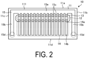
- FIG. 2 is a plan view of the head base 10 according to the first embodiment.
- the plurality of individual electrodes 14 are located on the first surface 111 side of the substrate 11, and is arranged along the arrangement direction of the heat generating unit 12.
- the individual electrode 14 includes one end 14a and the other end 14b.
- the one end 14a is electrically connected to the element of the heat generating unit 12.
- the other end 14b is electrically connected to the drive IC (not illustrated) located on the first surface 201 (see FIG. 1 ) of the wiring board 20 via a wire (not illustrated). Details of the individual electrode 14 will be described later.
- the common electrode 15 electrically connects each element of the heat generating unit 12 and the connector (not illustrated).
- the common electrode 15 includes a main wiring portion 15a, sub wiring portions 15b, and lead portions 15c.
- the main wiring portion 15a extends along one long side 11a of the substrate 11.
- the sub wiring portions 15b extend along each of one short side 11b and the other short side 11c of the substrate 11.
- the lead portions 15c individually extend from the main wiring portion 15a toward elements of the heat generating unit 12.
- the common electrode 15 is electrically connected to the connector (not illustrated) located on the wiring board 20 via wires (not illustrated) from end portions 15d.
- the common electrode 15 is located so as to surround the remaining three sides of the heat generating unit 12 excluding the other long side 11d side of the substrate 11 on which the individual electrodes 14 are disposed.
- the long side 11d is located adjacent to the wiring board 20. Note that the individual electrodes 14 and the common electrode 15 in FIG. 2 are schematically illustrated as an example and do not necessarily correspond to actual shapes.
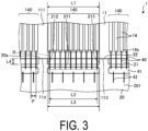
- FIG. 3 is a plan view illustrating a main part of the thermal head 1 according to the first embodiment.
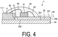
- FIG. 4 is a cross-sectional view illustrating the main part of the thermal head 1 according to the first embodiment.
- illustration of the resin member 30 is omitted.
- the thermal head 1 includes a plurality of individual electrode groups 140, a plurality of drive ICs 41, a plurality of first wires 40, and a plurality of second wires 42.
- Each of the plurality of individual electrode groups 140 includes a plurality of individual electrodes 14. Each of the individual electrodes 14 belonging to the individual electrode group 140 is electrically connected to the corresponding drive IC 41 via the first wire 40.
- the first wire 40 is an example of the wire member. In FIG. 3 , ten individual electrodes 14 are belonging to the individual electrode group 140, but the number of the individual electrodes 14 is not limited to ten and can be appropriately set.
- the plurality of drive ICs 41 are located along the first direction that is the arrangement direction of the heat generating unit 12 (see FIGS. 1 and 2 ). Each of the plurality of drive ICs 41 is located facing a corresponding individual electrode group 140.
- the drive IC 41 is electrically connected to the other end 14b of the individual electrode 14 on the substrate 11 via the first wire 40.
- the drive IC 41 is also electrically connected to a terminal (not illustrated) located on the first surface 201 of the wiring board 20 via the second wire 42.
- the drive IC 41 receives electrical signals supplied from the outside via the wiring board 20 and the second wire 42 electrically connected to the wiring board 20.
- the drive IC 41 supplies power to the heat generating unit 12 (see FIGS. 1 and 2 ) in accordance with received electrical signals to selectively cause each element of the heat generating unit 12 to generate heat.
- the plurality of first wires 40 each electrically connect the drive IC 41 and the individual electrodes 14 belonging to the individual electrode group 140 corresponding to the drive IC 41.
- the plurality of second wires 42 electrically connect the drive IC 41 and terminals (not illustrated) located on the first surface 201 of the wiring board 20.
- the first wire 40 and the second wire 42 are bonding wires made of a metal such as Cu, Au, Al, and the like.
- An interval P between the first wires 40 connected to the individual electrodes 14 belonging to the individual electrode group 140 may be, for example, 80 ⁇ m or less, or particularly 50 ⁇ m or more and 75 ⁇ m or less.
- the thermal head 1 further includes a plurality of recessed portions 21, a contact portion 22, and a connector 60.
- the plurality of recessed portions 21 are arranged side by side so as to face an end surface 113 of the substrate 11 on which the long side 11d of the substrate 11 is located. Each of the plurality of recessed portions 21 is located so as to be sandwiched between the individual electrode group 140 on the substrate 11 and the drive IC 41 on the wiring board 20.
- the plurality of recessed portions 21 are grooves formed by cutting out one end 20a of the wiring board 20 located facing the end surface 113. Further, the plurality of recessed portions 21 penetrate from the first surface 201 of the wiring board 20 to a second surface 202 that is a back surface of the wiring board 20. In this manner, the plurality of first wires 40 connecting the individual electrodes 14 and the drive IC 41 are located across the recessed portion 21.
- the contact portion 22 is located between the recessed portions 21 adjacent to each other.
- the contact portion 22 is the one end 20a of the wiring board 20 that is in contact with the end surface 113.
- the recessed portion 21 and the contact portion 22 are alternately located on the one end 20a of the wiring board 20.
- the connector 60 is located on the other end 20b side of the wiring board 20 located opposite to the one end 20a close to the substrate 11.
- the connector 60 is electrically connected to the wiring board 20 and is electrically connected to the outside.
- a flexible flat cable (not illustrated) electrically connecting the connector 60 and the wiring board 20 may be located between the connector 60 and the wiring board 20.
- the resin member 30 covers all the drive ICs 41 located on the wiring board 20.
- the resin member 30 is, for example, a silicone resin or an epoxy resin.
- the resin member 30 seals the drive ICs 41, the first wires 40, the second wires 42, and the like in a state in which the first wires 40 and the second wires 42 are connected to the drive ICs 41.
- the resin member 30 seals all regions illustrated in FIG. 3 .
- the resin member 30 is obtained by sealing a predetermined portion using a resin material having fluidity and then curing the resin material.
- a resin material having fluidity When the first wires 40 having a smaller interval P than the second wires 42 and the vicinity of the first wires 40 are sealed using the resin material, air bubbles are likely to be trapped in the resin material.
- some of the trapped air bubbles cannot be completely removed even after curing and may cause a crater-like depression on the surface of the resin member 30 or remain inside the resin member 30 as voids.
- the depression or voids generated in the resin member 30 as described above may cause performance failure such as an insufficient resistance value, in addition to an appearance defect.
- the plurality of first wires 40 are located across the plurality of recessed portions 21 located between the substrate 11 and the wiring board 20.
- the resin material for sealing the plurality of first wires 40 and the vicinity thereof is accumulated in a space defined by the first surface 501 of the heat dissipation plate 50, side surfaces 211 to 213 of the recessed portion 21, and the end surface 113.
- the resin material is further accumulated to a predetermined height so as to cover the plurality of first wires 40 located on the wiring board 20 and on the substrate 11 and then cured.
- the thermal head 1 it is possible to reduce the occurrence of failures due to the sealing using the resin member 30 such as entrapment of air bubbles into the resin material in the process of sealing the first wires 40 using the resin material and subsequent depression and voids of the resin member 30.
- the thermal head 1 according to the first embodiment includes the contact portion 22 located between the recessed portions 21 adjacent to each other, and the substrate 11 and the wiring board 20 are in contact with each other at the contact portion 22. Accordingly, the plurality of recessed portions 21 in which the resin material is accumulated are located only in areas overlapping in a plan view with the plurality of first wires 40 where the entrapment of air bubbles is likely to occur. Thus, according to the thermal head 1 according to the first embodiment an increase in the usage amount of the resin member 30 can be reduced.
- the contact portion 22 is located between the drive ICs 41 adjacent to each other and all of the recessed portions 21 facing the corresponding drive ICs 41.
- a length L1 of the recessed portion 21 along the first direction along which the plurality of recessed portions 21 are arranged can be larger than a width L2 along the first direction of a region R where the plurality of first wires 40 are located in a plan view.
- the length L1 of the recessed portion 21 can be smaller than a length L3 of the drive IC 41 along the first direction. This makes it possible to suppress an increase in the usage amount of the resin member 30. Further, it is possible to reduce the occurrence of failures such as exposure of the first wire 40 from the resin member 30.
- a length L4 of the recessed portion 21 in a second direction intersecting the first direction may be, for example, 50 ⁇ m or more and 200 ⁇ m or less, or further 80 ⁇ m or more and 100 ⁇ m or less. In one example, the length L4 may be 100 ⁇ m.
- the length L4 is less than 50 ⁇ m, it may be difficult for the resin material to enter the recessed portion 21, and appropriate sealing using the resin member 30 may not be achieved. On the other hand, when the length L4 exceeds 200 ⁇ m, the usage amount of the resin member 30 may be increased.
- the surface roughness of the side surfaces 211 to 213 of the recessed portion 21 may be larger than the surface roughness of the contact portion 22.
- the surface roughness of the side surfaces 211 to 213 of the recessed portions 21 may be larger than the surface roughness of the first surface 201 of the wiring board 20.
- the resin material having flowed to the first surface 201 of the wiring board 20 can easily enter the recessed portion 21, and the resin material having entered into the recessed portion 21 can be less likely to flow out of the recessed portion 21.
- appropriate sealing using the resin member 30 can be achieved.
- the magnitude of the surface roughness of the side surfaces 211 to 213, the contact portion 22, and the first surface 201 can be determined based on the arithmetic mean roughness Ra and the maximum height roughness Rz, defined in JIS B0633; 2001.
- the arithmetic mean roughness Ra and the maximum height roughness Rz can be measured, for example, by measuring in a sub scanning direction using a contact type or a non-contact type surface roughness meter. For example, when there is no significant difference in values of either of the arithmetic mean roughness Ra or the maximum height roughness Rz, the magnitude of the surface roughness can be determined in accordance with values of the other.
- the surface roughness of the side surfaces 211 to 213 is a value obtained by weighted averaging the measured values of the side surfaces 211 to 213 in accordance with the length L1 of the side surface 211 in the first direction and the length L4 of the side surfaces 212 and 213 in the second direction intersecting the first direction.
- the relationship between the length L1 of the recessed portion 21 and the length L3 of the drive IC 41 along the first direction is not limited to that described above. That is, the length L1 of the recessed portion 21 may be larger than the length L3 of the drive IC 41. This makes it possible to reduce the occurrence of failures due to the sealing using the resin member 30.
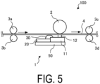
- FIG. 5 is a schematic view of the thermal printer 100 according to the first embodiment.
- the thermal printer 100 includes the thermal head 1, a platen roller 2, and a transport mechanism. Note that the thermal head 1 is attached to a housing (not illustrated) in a manner such that the arrangement direction of the heat generating unit 12 is along a main scanning direction that is a direction orthogonal to a transport direction of a recording paper 4 that is a recording medium.
- the transport mechanism includes a drive unit (not illustrated) and transport rollers 3a to 3d.
- the transport mechanism transports the recording paper 4 in an arrow direction illustrated in FIG. 5 onto the heat generating unit 12 of the thermal head 1.
- the drive unit has a function of driving the transport rollers 3a to 3d.
- the drive unit may include, for example, a motor.
- the transport rollers 3a to 3d may be made, for example, by covering a shaft body having a cylindrical shape and made of a metal such as stainless steel, using an elastic member made of butadiene rubber or the like.
- the platen roller 2 presses the recording paper 4 onto the heat generating unit 12 of the thermal head 1.
- the platen roller 2 is located so as to extend in a direction (the main scanning direction) orthogonal to the transport direction of the recording paper 4, and both end portions are supported and fixed to be rotatable in a state in which the recording paper 4 is pressed onto the heat generating unit 12.
- the platen roller 2 may be made, for example, by covering a cylindrical shaft body made of a metal such as stainless steel or the like, with an elastic member made of butadiene rubber or the like.
- the thermal printer 100 selectively causes respective elements of the heat generating unit 12 to generate heat while pressing the recording paper 4 onto the heat generating unit 12 of the thermal head 1 using the platen roller 2 and transporting the recording paper 4 onto the heat generating unit 12 by the transport mechanism. By the series of operations described above, the thermal printer 100 performs predetermined printing on the recording paper 4.
- FIG. 6 is a perspective view illustrating a configuration of a thermal head 1A according to a second embodiment.
- the thermal head 1A according to the second embodiment differs from the thermal head 1 according to the first embodiment in that, in the thermal head 1A, a plurality of recessed portions 21A include bottom surfaces 214 so as to be bottomed openings in which a first surface 201 side of a wiring board 20 is open, while the thermal head 1 includes the plurality of recessed portions 21 that penetrate through the wiring board 20 in a thickness direction.
- a resin material for sealing a plurality of first wires 40 and the vicinity thereof is accumulated in a space defined by the bottom surface 214 of the recessed portion 21A, side surfaces 211 to 213 of the recessed portion 21, and the end surface 113 (see FIG. 3 ). Then, the resin material is further accumulated to a predetermined height so as to cover the plurality of first wires 40 located on the wiring board 20 and on a substrate 11 and then cured.
- an increase in the usage amount of the resin member 30 can be further reduced as compared to the thermal head 1 including the plurality of recessed portions 21 that penetrate through the wiring board 20 in the thickness direction.
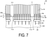
- FIG. 7 is a plan view illustrating a main part of a thermal head 1B according to a third embodiment.
- FIG. 8 is a cross-sectional view illustrating the main part of the thermal head 1B according to the third embodiment.
- the thermal head 1B according to the third embodiment differs from the thermal heads 1 and 1A in that a plurality of recessed portions 16 and a contact portion 17 are located on an end surface 113 side of a substrate 11.
- the plurality of recessed portions 16 are located so as to face one end 20a of a wiring board 20.
- the plurality of recessed portions 16 are grooves that penetrate from a first surface 111 to a second surface 112 of the substrate 11 so as to cut out the end surface 113 of the substrate 11 located facing the one end 20a.
- the contact portion 17 is located between the recessed portions 16 adjacent to each other.
- the contact portion 17 is the end surface 113 of the substrate 11 that is in contact with the one end 20a of the wiring board 20. That is, the recessed portion 16 and the contact portion 17 are alternately located on the end surface 113 of the substrate 11.
- a resin material for sealing a plurality of first wires 40 and the vicinity thereof is accumulated in a space defined by a first surface 501 of a heat dissipation plate 50, the recessed portion 16, and the one end 20a. Then, the resin material is further accumulated to a predetermined height so as to cover the plurality of first wires 40 located on the wiring board 20 and on the substrate 11 and then cured.
- the thermal head 1B according to the third embodiment it is possible to reduce the occurrence of entrapment of air bubbles into the resin material in the process of sealing the first wires 40 using the resin material and subsequent failures due to the sealing using the resin member 30.
- the thermal head 1B according to the third embodiment includes a contact portion 17 located between the recessed portions 16 adjacent to each other, and the substrate 11 and the wiring board 20 are in contact with each other at the contact portion 17. Accordingly, the plurality of recessed portions 16 in which the resin material is accumulated are located only in areas overlapping in a plan view with the plurality of first wires 40 where the entrapment of air bubbles is likely to occur. Thus, according to the thermal head 1B according to the third embodiment, an increase in the usage amount of the resin member 30 can be suppressed.
- a length L5 of the recessed portion 16 in a second direction intersecting a first direction may be, for example, 50 ⁇ m or more and 200 ⁇ m or less, or further 80 ⁇ m or more and 100 ⁇ m or less. In one example, the length L5 may be 100 ⁇ m.
- the length L5 is less than 50 ⁇ m, it may be difficult for the resin material to enter the recessed portion 16, and appropriate sealing using the resin member 30 may not be achieved. On the other hand, when the length L5 exceeds 200 ⁇ m, the usage amount of the resin member 30 may be increased.
- thermal printer 100 including the thermal head 1 according to the first embodiment has been described, the present invention is not limited thereto, and the thermal head 1A or 1B according to other embodiments may be included in the thermal printer 100. In addition, the thermal heads 1 to 1B according to the plurality of embodiments may be combined.
- either of the substrate 11 or the wiring board 20 includes the plurality of recessed portions and the contact portions, but the present invention is not limited thereto, and both of the substrate 11 and the wiring board 20 may include the plurality of recessed portions and the contact portions.
- the thermal head 1 (1A, 1B) includes the head base 10, the wiring board 20, the plurality of recessed portions 21 (21A, 16), the contact portions 17, the plurality of drive ICs 41, and the plurality of wire members (first wires 40), and the resin member 30.
- the head base 10 includes the substrate 11.
- the wiring board 20 is located adjacent to the head base 10.
- the plurality of recessed portions 21 are located adjacent to the head base 10.
- the contact portion 17 is located between the recessed portions 21 adjacent to each other, and the substrate 11 and the wiring board 20 are in contact with each other at the contact portion 17.
- the plurality of drive ICs 41 are located on the first surface 201 of the wiring board 20 so as to face one by one the plurality of recessed portions 21.
- the plurality of wire members are located across the recessed portions 21 and electrically connect the substrate 11 and the drive ICs 41.
- the resin member 30 seals the plurality of wire members (first wires 40) and the plurality of drive ICs 41.
- the thermal head 1 (1A, 1B) according to the embodiments can reduce the occurrence of failures due to the sealing using the resin member 30 while suppressing the usage amount of the resin member 30.
Landscapes
- Electronic Switches (AREA)
Claims (12)
- Thermokopf (1), aufweisend:eine Kopfbasis (10), aufweisendein Substrat (11),eine Wärmespeicherschicht (13), die auf einer ersten Fläche (111) des Substrats (11) entlang einer Längsrichtung des Substrats (11) angeordnet ist,eine Wärmeerzeugungseinheit (12), die auf der Wärmespeicherschicht (13) angeordnet ist, die aus einer Mehrzahl von Elementen gebildet ist, die entlang der Längsrichtung des Substrats (11) angeordnet sind,eine Mehrzahl einzelner Elektroden (14), die nebeneinander auf einer Seite der Wärmeerzeugungseinheit (12) auf der erste-Fläche- (111) Seite des Substrats (11) angeordnet sind, die einzeln eine nach der anderen mit den Elementen der Wärmeerzeugungseinheit (12) verbunden sind, undeine gemeinsame Elektrode (15), die auf der ersten Fläche (111) des Substrats (11) angeordnet ist, um die verbleibenden drei Seiten der Wärmeerzeugungseinheit (12) zu umgeben, die mit allen der Elemente der Wärmeerzeugungseinheit (12) gemeinsam verbunden ist,eine Verdrahtungsplatte (20), die benachbart zu der Kopfbasis (10) angeordnet ist,eine Wärmeabführplatte (50), die auf einer zweite-Fläche (112) Seite des Substrats (11) und auf einer zweite-Fläche (202) Seite der Verdrahtungsplatte (20) angeordnet ist,eine Mehrzahl von Aussparungsabschnitten (16), die zwischen dem Substrat (11) und der Verdrahtungsplatte (20) angeordnet sind,einen Kontaktabschnitt (17), der zwischen benachbarten Aussparungsabschnitten (16) der Mehrzahl von Aussparungsabschnitten (16) angeordnet ist, wobei der Kontaktabschnitt (17) konfiguriert ist, um mit dem Substrat (11) und der Verdrahtungsplatte (20) in Kontakt zu kommen,eine Mehrzahl von Treiber-ICs (41), die auf einer ersten Fläche der Verdrahtungsplatte (20) angeordnet sind, um einem jeweiligen korrespondierenden Aussparungsabschnitt (16) der Mehrzahl von Aussparungsabschnitten (16) zugewandt zu sein,eine Mehrzahl von Drahtelementen, die über die Mehrzahl von Aussparungsabschnitten (16) angeordnet sind, wobei die Mehrzahl von Drahtelementen konfiguriert ist, um das Substrat (11) und die Mehrzahl von Treiber-ICs (41) elektrisch zu verbinden, undein Harzelement (30), das konfiguriert ist, um die Mehrzahl von Drahtelementen und die Mehrzahl von Treiber-ICs (41) abzudichten.
- Thermokopf (1) gemäß Anspruch 1, wobei
der Kontaktabschnitt (17) zwischen benachbarten Treiber-ICs (41) der Mehrzahl von Treiber-ICs (41) angeordnet ist und alle Aussparungsabschnitte (16) der Mehrzahl von Aussparungsabschnitten (16) einem korrespondierenden Treiber-IC (41) der Mehrzahl von Treiber-ICs (41) zugewandt sind. - Thermokopf (1) gemäß Anspruch 1 oder 2, wobei
eine Länge jedes Aussparungsabschnitts (16) der Mehrzahl von Aussparungsabschnitten (16) entlang einer ersten Richtung, entlang der die Mehrzahl von Aussparungsabschnitten (16) angeordnet ist, in einer Draufsicht größer als eine Breite entlang der ersten Richtung eines Bereichs ist, wo die Mehrzahl von Drahtelementen angeordnet ist. - Thermokopf (1) gemäß irgendeinem der Ansprüche 1 bis 3, wobei
eine Länge jedes Aussparungsabschnitts (16) der Mehrzahl von Aussparungsabschnitten (16) entlang einer ersten Richtung, entlang der die Mehrzahl von Aussparungsabschnitten (16) angeordnet ist, kleiner als eine Länge jedes Treiber-ICs (41) der Mehrzahl von Treiber-ICs (41) entlang der ersten Richtung ist. - Thermokopf (1) gemäß irgendeinem der Ansprüche 1 bis 3, wobei
eine Länge jedes Aussparungsabschnitts (16) der Mehrzahl von Aussparungsabschnitten (16) entlang einer ersten Richtung, entlang der die Mehrzahl von Aussparungsabschnitten (16) angeordnet ist, größer als eine Länge jedes Treiber-ICs (41) der Mehrzahl von Treiber-ICs (41) entlang der ersten Richtung ist. - Thermokopf (1) gemäß irgendeinem der Ansprüche 1 bis 5, wobeidie Mehrzahl von Aussparungsabschnitten (16) auf der Verdrahtungsplatte (20) angeordnet ist und dem Substrat (11) zugewandt ist, undeine Oberflächenrauigkeit von Seitenflächen jedes Aussparungsabschnitts (16) der Mehrzahl von Aussparungsabschnitten (16) größer als eine Oberflächenrauigkeit des Kontaktabschnitts (17) ist.
- Thermokopf (1) gemäß irgendeinem der Ansprüche 1 bis 6, wobeidie Mehrzahl von Aussparungsabschnitten (16) auf der Verdrahtungsplatte (20) angeordnet ist und dem Substrat (11) zugewandt ist, undeine Oberflächenrauigkeit von Seitenflächen jedes Aussparungsabschnitts (16) der Aussparungsabschnitte (16) größer als eine Oberflächenrauigkeit der ersten Fläche ist.
- Thermokopf (1) gemäß irgendeinem der Ansprüche 1 bis 7,
wobei die Mehrzahl von Aussparungsabschnitten (16) die Verdrahtungsplatte (20) in einer Dickenrichtung durchdringt. - Thermokopf (1) gemäß irgendeinem der Ansprüche 1 bis 7, wobei
jeder Aussparungsabschnitt (16) der Mehrzahl von Aussparungsabschnitten (16) eine Bodenfläche und eine Öffnung in der ersten Fläche der Verdrahtungsplatte (20) hat. - Thermokopf (1) gemäß irgendeinem der Ansprüche 1 bis 9, wobei
die Mehrzahl von Aussparungsabschnitten (16) das Substrat (11) in einer Dickenrichtung durchdringt. - Thermokopf (1) gemäß irgendeinem der Ansprüche 1 bis 10, wobei die Wärmeabführplatte (50) das Substrat (11) und die auf einer ersten Fläche der Wärmeabführplatte (50) angeordnete Verdrahtungsplatte (20) aufweist.
- Thermodrucker (100), aufweisend:den Thermokopf (1) gemäß irgendeinem der Ansprüche 1 bis 11,einen Transportmechanismus, der konfiguriert ist, um ein Aufzeichnungsmedium auf die Wärmeerzeugungseinheit (12) zu transportieren, die auf dem Substrat (11) vorgesehen ist, undeine Druckwalze, die konfiguriert ist, um das Aufzeichnungsmedium auf die Wärmeerzeugungseinheit (12) zu drücken.
Applications Claiming Priority (2)
| Application Number | Priority Date | Filing Date | Title |
|---|---|---|---|
| JP2019211866 | 2019-11-22 | ||
| PCT/JP2020/043259 WO2021100822A1 (ja) | 2019-11-22 | 2020-11-19 | サーマルヘッドおよびサーマルプリンタ |
Publications (3)
| Publication Number | Publication Date |
|---|---|
| EP4063134A1 EP4063134A1 (de) | 2022-09-28 |
| EP4063134A4 EP4063134A4 (de) | 2023-11-22 |
| EP4063134B1 true EP4063134B1 (de) | 2024-11-06 |
Family
ID=75966372
Family Applications (1)
| Application Number | Title | Priority Date | Filing Date |
|---|---|---|---|
| EP20891337.6A Active EP4063134B1 (de) | 2019-11-22 | 2020-11-19 | Thermodruckkopf und thermodrucker |
Country Status (4)
| Country | Link |
|---|---|
| US (1) | US11731433B2 (de) |
| EP (1) | EP4063134B1 (de) |
| JP (1) | JP6875616B1 (de) |
| CN (1) | CN114746275B (de) |
Family Cites Families (21)
| Publication number | Priority date | Publication date | Assignee | Title |
|---|---|---|---|---|
| JPS60110470A (ja) * | 1983-11-21 | 1985-06-15 | Konishiroku Photo Ind Co Ltd | 感熱記録ヘッド |
| JPH0243058A (ja) * | 1988-08-04 | 1990-02-13 | Nhk Spring Co Ltd | 基板の封止構造 |
| JP2590566Y2 (ja) * | 1992-08-12 | 1999-02-17 | アオイ電子株式会社 | サーマルプリントヘッド |
| JP3403806B2 (ja) * | 1994-06-01 | 2003-05-06 | 株式会社東芝 | サーマルヘッド |
| US6028619A (en) * | 1997-10-06 | 2000-02-22 | Seiko Instruments Inc. | Thermal head |
| JP4398766B2 (ja) * | 2004-03-30 | 2010-01-13 | アルプス電気株式会社 | サーマルヘッド及びその製造方法 |
| JP4476669B2 (ja) * | 2004-03-30 | 2010-06-09 | アルプス電気株式会社 | サーマルヘッド及びその製造方法 |
| JP2006035722A (ja) * | 2004-07-29 | 2006-02-09 | Kyocera Corp | サーマルヘッド及びサーマルプリンタ |
| JP4628266B2 (ja) * | 2005-12-27 | 2011-02-09 | アルプス電気株式会社 | サーマルヘッドの製造方法 |
| JP5174287B1 (ja) * | 2011-03-25 | 2013-04-03 | 京セラ株式会社 | サーマルヘッドおよびこれを備えるサーマルプリンタ |
| JP2014188682A (ja) * | 2013-03-26 | 2014-10-06 | Toshiba Hokuto Electronics Corp | サーマルプリントヘッドおよびその製造方法 |
| JP6130510B2 (ja) * | 2013-08-26 | 2017-05-17 | 京セラ株式会社 | サーマルヘッドおよびこれを備えるサーマルプリンタ |
| WO2016068313A1 (ja) * | 2014-10-30 | 2016-05-06 | 京セラ株式会社 | サーマルヘッド、およびサーマルプリンタ |
| JP6618932B2 (ja) * | 2015-01-16 | 2019-12-11 | ローム株式会社 | サーマルプリントヘッド |
| JP6419006B2 (ja) * | 2015-03-27 | 2018-11-07 | 京セラ株式会社 | サーマルヘッドおよびサーマルプリンタ |
| CN108025559B (zh) * | 2015-09-26 | 2019-09-27 | 京瓷株式会社 | 热敏头以及热敏式打印机 |
| JP6598717B2 (ja) * | 2016-03-29 | 2019-10-30 | 京セラ株式会社 | サーマルヘッドおよびサーマルプリンタ |
| JP2018051973A (ja) * | 2016-09-29 | 2018-04-05 | 東芝ホクト電子株式会社 | サーマルプリントヘッド |
| WO2018181734A1 (ja) * | 2017-03-29 | 2018-10-04 | 京セラ株式会社 | サーマルヘッドおよびサーマルプリンタ |
| US10543696B2 (en) * | 2017-06-08 | 2020-01-28 | Rohm Co., Ltd. | Thermal print head |
| JP6971751B2 (ja) * | 2017-09-29 | 2021-11-24 | 京セラ株式会社 | サーマルヘッド及びサーマルプリンタ |
-
2020
- 2020-11-19 US US17/778,401 patent/US11731433B2/en active Active
- 2020-11-19 JP JP2021509931A patent/JP6875616B1/ja active Active
- 2020-11-19 CN CN202080080558.9A patent/CN114746275B/zh active Active
- 2020-11-19 EP EP20891337.6A patent/EP4063134B1/de active Active
Also Published As
| Publication number | Publication date |
|---|---|
| US20220396081A1 (en) | 2022-12-15 |
| EP4063134A4 (de) | 2023-11-22 |
| EP4063134A1 (de) | 2022-09-28 |
| US11731433B2 (en) | 2023-08-22 |
| JP6875616B1 (ja) | 2021-05-26 |
| CN114746275B (zh) | 2023-06-30 |
| CN114746275A (zh) | 2022-07-12 |
| JPWO2021100822A1 (ja) | 2021-12-02 |
Similar Documents
| Publication | Publication Date | Title |
|---|---|---|
| US10099486B2 (en) | Thermal head and thermal printer | |
| CN110509672B (zh) | 热敏打印头 | |
| US9701131B2 (en) | Thermal head and thermal printer | |
| CN107405929B (zh) | 热敏头、热敏打印机以及热敏头的制造方法 | |
| US10981396B2 (en) | Thermal head and thermal printer | |
| EP4063134B1 (de) | Thermodruckkopf und thermodrucker | |
| CN105408119B (zh) | 热敏头及具备该热敏头的热敏打印机 | |
| US9937728B2 (en) | Thermal head and thermal printer | |
| EP3928992B1 (de) | Thermodruckkopf und thermodrucker | |
| US12145379B2 (en) | Thermal head and thermal printer | |
| JP7267905B2 (ja) | サーマルヘッド及びサーマルプリンタ | |
| US9834008B2 (en) | Thermal head and thermal printer | |
| US10596826B2 (en) | Thermal head and thermal printer | |
| US9744775B2 (en) | Thermal head and thermal printer | |
| WO2021100822A1 (ja) | サーマルヘッドおよびサーマルプリンタ | |
| JP5852387B2 (ja) | サーマルプリントヘッド | |
| JP2009131994A (ja) | サーマルプリントヘッドおよびその製造方法 | |
| US10525730B2 (en) | Thermal head and thermal printer | |
| JP6632449B2 (ja) | サーマルヘッドおよびサーマルプリンタ | |
| JP2018138345A (ja) | サーマルプリントヘッドおよびその製造方法 |
Legal Events
| Date | Code | Title | Description |
|---|---|---|---|
| STAA | Information on the status of an ep patent application or granted ep patent |
Free format text: STATUS: THE INTERNATIONAL PUBLICATION HAS BEEN MADE |
|
| PUAI | Public reference made under article 153(3) epc to a published international application that has entered the european phase |
Free format text: ORIGINAL CODE: 0009012 |
|
| STAA | Information on the status of an ep patent application or granted ep patent |
Free format text: STATUS: REQUEST FOR EXAMINATION WAS MADE |
|
| 17P | Request for examination filed |
Effective date: 20220519 |
|
| AK | Designated contracting states |
Kind code of ref document: A1 Designated state(s): AL AT BE BG CH CY CZ DE DK EE ES FI FR GB GR HR HU IE IS IT LI LT LU LV MC MK MT NL NO PL PT RO RS SE SI SK SM TR |
|
| DAV | Request for validation of the european patent (deleted) | ||
| DAX | Request for extension of the european patent (deleted) | ||
| P01 | Opt-out of the competence of the unified patent court (upc) registered |
Effective date: 20230508 |
|
| A4 | Supplementary search report drawn up and despatched |
Effective date: 20231025 |
|
| RIC1 | Information provided on ipc code assigned before grant |
Ipc: B41J 2/345 20060101ALI20231019BHEP Ipc: B41J 2/335 20060101AFI20231019BHEP |
|
| GRAP | Despatch of communication of intention to grant a patent |
Free format text: ORIGINAL CODE: EPIDOSNIGR1 |
|
| STAA | Information on the status of an ep patent application or granted ep patent |
Free format text: STATUS: GRANT OF PATENT IS INTENDED |
|
| INTG | Intention to grant announced |
Effective date: 20240604 |
|
| GRAS | Grant fee paid |
Free format text: ORIGINAL CODE: EPIDOSNIGR3 |
|
| GRAA | (expected) grant |
Free format text: ORIGINAL CODE: 0009210 |
|
| STAA | Information on the status of an ep patent application or granted ep patent |
Free format text: STATUS: THE PATENT HAS BEEN GRANTED |
|
| AK | Designated contracting states |
Kind code of ref document: B1 Designated state(s): AL AT BE BG CH CY CZ DE DK EE ES FI FR GB GR HR HU IE IS IT LI LT LU LV MC MK MT NL NO PL PT RO RS SE SI SK SM TR |
|
| REG | Reference to a national code |
Ref country code: GB Ref legal event code: FG4D |
|
| REG | Reference to a national code |
Ref country code: CH Ref legal event code: EP |
|
| REG | Reference to a national code |
Ref country code: DE Ref legal event code: R096 Ref document number: 602020041073 Country of ref document: DE |
|
| REG | Reference to a national code |
Ref country code: IE Ref legal event code: FG4D |
|
| REG | Reference to a national code |
Ref country code: LT Ref legal event code: MG9D |
|
| REG | Reference to a national code |
Ref country code: NL Ref legal event code: MP Effective date: 20241106 |
|
| PG25 | Lapsed in a contracting state [announced via postgrant information from national office to epo] |
Ref country code: IS Free format text: LAPSE BECAUSE OF FAILURE TO SUBMIT A TRANSLATION OF THE DESCRIPTION OR TO PAY THE FEE WITHIN THE PRESCRIBED TIME-LIMIT Effective date: 20250306 Ref country code: PT Free format text: LAPSE BECAUSE OF FAILURE TO SUBMIT A TRANSLATION OF THE DESCRIPTION OR TO PAY THE FEE WITHIN THE PRESCRIBED TIME-LIMIT Effective date: 20250306 Ref country code: HR Free format text: LAPSE BECAUSE OF FAILURE TO SUBMIT A TRANSLATION OF THE DESCRIPTION OR TO PAY THE FEE WITHIN THE PRESCRIBED TIME-LIMIT Effective date: 20241106 |
|
| PG25 | Lapsed in a contracting state [announced via postgrant information from national office to epo] |
Ref country code: FI Free format text: LAPSE BECAUSE OF FAILURE TO SUBMIT A TRANSLATION OF THE DESCRIPTION OR TO PAY THE FEE WITHIN THE PRESCRIBED TIME-LIMIT Effective date: 20241106 Ref country code: NL Free format text: LAPSE BECAUSE OF FAILURE TO SUBMIT A TRANSLATION OF THE DESCRIPTION OR TO PAY THE FEE WITHIN THE PRESCRIBED TIME-LIMIT Effective date: 20241106 |
|
| REG | Reference to a national code |
Ref country code: AT Ref legal event code: MK05 Ref document number: 1738989 Country of ref document: AT Kind code of ref document: T Effective date: 20241106 |
|
| PG25 | Lapsed in a contracting state [announced via postgrant information from national office to epo] |
Ref country code: BG Free format text: LAPSE BECAUSE OF FAILURE TO SUBMIT A TRANSLATION OF THE DESCRIPTION OR TO PAY THE FEE WITHIN THE PRESCRIBED TIME-LIMIT Effective date: 20241106 |
|
| PG25 | Lapsed in a contracting state [announced via postgrant information from national office to epo] |
Ref country code: ES Free format text: LAPSE BECAUSE OF FAILURE TO SUBMIT A TRANSLATION OF THE DESCRIPTION OR TO PAY THE FEE WITHIN THE PRESCRIBED TIME-LIMIT Effective date: 20241106 |
|
| PG25 | Lapsed in a contracting state [announced via postgrant information from national office to epo] |
Ref country code: NO Free format text: LAPSE BECAUSE OF FAILURE TO SUBMIT A TRANSLATION OF THE DESCRIPTION OR TO PAY THE FEE WITHIN THE PRESCRIBED TIME-LIMIT Effective date: 20250206 |
|
| PG25 | Lapsed in a contracting state [announced via postgrant information from national office to epo] |
Ref country code: LV Free format text: LAPSE BECAUSE OF FAILURE TO SUBMIT A TRANSLATION OF THE DESCRIPTION OR TO PAY THE FEE WITHIN THE PRESCRIBED TIME-LIMIT Effective date: 20241106 Ref country code: GR Free format text: LAPSE BECAUSE OF FAILURE TO SUBMIT A TRANSLATION OF THE DESCRIPTION OR TO PAY THE FEE WITHIN THE PRESCRIBED TIME-LIMIT Effective date: 20250207 Ref country code: AT Free format text: LAPSE BECAUSE OF FAILURE TO SUBMIT A TRANSLATION OF THE DESCRIPTION OR TO PAY THE FEE WITHIN THE PRESCRIBED TIME-LIMIT Effective date: 20241106 |
|
| PG25 | Lapsed in a contracting state [announced via postgrant information from national office to epo] |
Ref country code: PL Free format text: LAPSE BECAUSE OF FAILURE TO SUBMIT A TRANSLATION OF THE DESCRIPTION OR TO PAY THE FEE WITHIN THE PRESCRIBED TIME-LIMIT Effective date: 20241106 |
|
| PG25 | Lapsed in a contracting state [announced via postgrant information from national office to epo] |
Ref country code: RS Free format text: LAPSE BECAUSE OF FAILURE TO SUBMIT A TRANSLATION OF THE DESCRIPTION OR TO PAY THE FEE WITHIN THE PRESCRIBED TIME-LIMIT Effective date: 20250206 |
|
| REG | Reference to a national code |
Ref country code: CH Ref legal event code: PL |
|
| PG25 | Lapsed in a contracting state [announced via postgrant information from national office to epo] |
Ref country code: SM Free format text: LAPSE BECAUSE OF FAILURE TO SUBMIT A TRANSLATION OF THE DESCRIPTION OR TO PAY THE FEE WITHIN THE PRESCRIBED TIME-LIMIT Effective date: 20241106 |
|
| PG25 | Lapsed in a contracting state [announced via postgrant information from national office to epo] |
Ref country code: DK Free format text: LAPSE BECAUSE OF FAILURE TO SUBMIT A TRANSLATION OF THE DESCRIPTION OR TO PAY THE FEE WITHIN THE PRESCRIBED TIME-LIMIT Effective date: 20241106 |
|
| PG25 | Lapsed in a contracting state [announced via postgrant information from national office to epo] |
Ref country code: LU Free format text: LAPSE BECAUSE OF NON-PAYMENT OF DUE FEES Effective date: 20241119 |
|
| REG | Reference to a national code |
Ref country code: CH Ref legal event code: PL |
|
| PG25 | Lapsed in a contracting state [announced via postgrant information from national office to epo] |
Ref country code: EE Free format text: LAPSE BECAUSE OF FAILURE TO SUBMIT A TRANSLATION OF THE DESCRIPTION OR TO PAY THE FEE WITHIN THE PRESCRIBED TIME-LIMIT Effective date: 20241106 |
|
| PG25 | Lapsed in a contracting state [announced via postgrant information from national office to epo] |
Ref country code: CH Free format text: LAPSE BECAUSE OF NON-PAYMENT OF DUE FEES Effective date: 20241130 |
|
| PG25 | Lapsed in a contracting state [announced via postgrant information from national office to epo] |
Ref country code: RO Free format text: LAPSE BECAUSE OF FAILURE TO SUBMIT A TRANSLATION OF THE DESCRIPTION OR TO PAY THE FEE WITHIN THE PRESCRIBED TIME-LIMIT Effective date: 20241106 |
|
| PG25 | Lapsed in a contracting state [announced via postgrant information from national office to epo] |
Ref country code: SK Free format text: LAPSE BECAUSE OF FAILURE TO SUBMIT A TRANSLATION OF THE DESCRIPTION OR TO PAY THE FEE WITHIN THE PRESCRIBED TIME-LIMIT Effective date: 20241106 |
|
| PG25 | Lapsed in a contracting state [announced via postgrant information from national office to epo] |
Ref country code: CZ Free format text: LAPSE BECAUSE OF FAILURE TO SUBMIT A TRANSLATION OF THE DESCRIPTION OR TO PAY THE FEE WITHIN THE PRESCRIBED TIME-LIMIT Effective date: 20241106 |
|
| PG25 | Lapsed in a contracting state [announced via postgrant information from national office to epo] |
Ref country code: IT Free format text: LAPSE BECAUSE OF FAILURE TO SUBMIT A TRANSLATION OF THE DESCRIPTION OR TO PAY THE FEE WITHIN THE PRESCRIBED TIME-LIMIT Effective date: 20241106 |
|
| REG | Reference to a national code |
Ref country code: DE Ref legal event code: R097 Ref document number: 602020041073 Country of ref document: DE |
|
| REG | Reference to a national code |
Ref country code: BE Ref legal event code: MM Effective date: 20241130 |
|
| PG25 | Lapsed in a contracting state [announced via postgrant information from national office to epo] |
Ref country code: SE Free format text: LAPSE BECAUSE OF FAILURE TO SUBMIT A TRANSLATION OF THE DESCRIPTION OR TO PAY THE FEE WITHIN THE PRESCRIBED TIME-LIMIT Effective date: 20241106 |
|
| PLBE | No opposition filed within time limit |
Free format text: ORIGINAL CODE: 0009261 |
|
| STAA | Information on the status of an ep patent application or granted ep patent |
Free format text: STATUS: NO OPPOSITION FILED WITHIN TIME LIMIT |
|
| PG25 | Lapsed in a contracting state [announced via postgrant information from national office to epo] |
Ref country code: MC Free format text: LAPSE BECAUSE OF FAILURE TO SUBMIT A TRANSLATION OF THE DESCRIPTION OR TO PAY THE FEE WITHIN THE PRESCRIBED TIME-LIMIT Effective date: 20241106 |
|
| 26N | No opposition filed |
Effective date: 20250807 |
|
| PG25 | Lapsed in a contracting state [announced via postgrant information from national office to epo] |
Ref country code: BE Free format text: LAPSE BECAUSE OF NON-PAYMENT OF DUE FEES Effective date: 20241130 |
|
| PGFP | Annual fee paid to national office [announced via postgrant information from national office to epo] |
Ref country code: FR Payment date: 20250930 Year of fee payment: 6 |
|
| PG25 | Lapsed in a contracting state [announced via postgrant information from national office to epo] |
Ref country code: IE Free format text: LAPSE BECAUSE OF NON-PAYMENT OF DUE FEES Effective date: 20241119 |
|
| PGFP | Annual fee paid to national office [announced via postgrant information from national office to epo] |
Ref country code: DE Payment date: 20250930 Year of fee payment: 6 |
|
| PGFP | Annual fee paid to national office [announced via postgrant information from national office to epo] |
Ref country code: GB Payment date: 20251001 Year of fee payment: 6 |
|
| PG25 | Lapsed in a contracting state [announced via postgrant information from national office to epo] |
Ref country code: HU Free format text: LAPSE BECAUSE OF FAILURE TO SUBMIT A TRANSLATION OF THE DESCRIPTION OR TO PAY THE FEE WITHIN THE PRESCRIBED TIME-LIMIT; INVALID AB INITIO Effective date: 20201119 |
|
| PG25 | Lapsed in a contracting state [announced via postgrant information from national office to epo] |
Ref country code: CY Free format text: LAPSE BECAUSE OF FAILURE TO SUBMIT A TRANSLATION OF THE DESCRIPTION OR TO PAY THE FEE WITHIN THE PRESCRIBED TIME-LIMIT; INVALID AB INITIO Effective date: 20201119 |