EP4053904A1 - Anzeigesubstrat, herstellungsverfahren dafür und anzeigevorrichtung - Google Patents
Anzeigesubstrat, herstellungsverfahren dafür und anzeigevorrichtung Download PDFInfo
- Publication number
- EP4053904A1 EP4053904A1 EP20870454.4A EP20870454A EP4053904A1 EP 4053904 A1 EP4053904 A1 EP 4053904A1 EP 20870454 A EP20870454 A EP 20870454A EP 4053904 A1 EP4053904 A1 EP 4053904A1
- Authority
- EP
- European Patent Office
- Prior art keywords
- electrode
- pixel
- sub
- layer
- base substrate
- Prior art date
- Legal status (The legal status is an assumption and is not a legal conclusion. Google has not performed a legal analysis and makes no representation as to the accuracy of the status listed.)
- Granted
Links
Images


Classifications
-
- H—ELECTRICITY
- H10—SEMICONDUCTOR DEVICES; ELECTRIC SOLID-STATE DEVICES NOT OTHERWISE PROVIDED FOR
- H10K—ORGANIC ELECTRIC SOLID-STATE DEVICES
- H10K59/00—Integrated devices, or assemblies of multiple devices, comprising at least one organic light-emitting element covered by group H10K50/00
- H10K59/10—OLED displays
- H10K59/12—Active-matrix OLED [AMOLED] displays
-
- H—ELECTRICITY
- H10—SEMICONDUCTOR DEVICES; ELECTRIC SOLID-STATE DEVICES NOT OTHERWISE PROVIDED FOR
- H10D—INORGANIC ELECTRIC SEMICONDUCTOR DEVICES
- H10D84/00—Integrated devices formed in or on semiconductor substrates that comprise only semiconducting layers, e.g. on Si wafers or on GaAs-on-Si wafers
- H10D84/01—Manufacture or treatment
-
- H—ELECTRICITY
- H10—SEMICONDUCTOR DEVICES; ELECTRIC SOLID-STATE DEVICES NOT OTHERWISE PROVIDED FOR
- H10K—ORGANIC ELECTRIC SOLID-STATE DEVICES
- H10K59/00—Integrated devices, or assemblies of multiple devices, comprising at least one organic light-emitting element covered by group H10K50/00
- H10K59/10—OLED displays
- H10K59/12—Active-matrix OLED [AMOLED] displays
- H10K59/121—Active-matrix OLED [AMOLED] displays characterised by the geometry or disposition of pixel elements
- H10K59/1213—Active-matrix OLED [AMOLED] displays characterised by the geometry or disposition of pixel elements the pixel elements being TFTs
-
- H—ELECTRICITY
- H10—SEMICONDUCTOR DEVICES; ELECTRIC SOLID-STATE DEVICES NOT OTHERWISE PROVIDED FOR
- H10K—ORGANIC ELECTRIC SOLID-STATE DEVICES
- H10K59/00—Integrated devices, or assemblies of multiple devices, comprising at least one organic light-emitting element covered by group H10K50/00
- H10K59/10—OLED displays
- H10K59/12—Active-matrix OLED [AMOLED] displays
- H10K59/121—Active-matrix OLED [AMOLED] displays characterised by the geometry or disposition of pixel elements
- H10K59/1216—Active-matrix OLED [AMOLED] displays characterised by the geometry or disposition of pixel elements the pixel elements being capacitors
-
- H—ELECTRICITY
- H10—SEMICONDUCTOR DEVICES; ELECTRIC SOLID-STATE DEVICES NOT OTHERWISE PROVIDED FOR
- H10K—ORGANIC ELECTRIC SOLID-STATE DEVICES
- H10K59/00—Integrated devices, or assemblies of multiple devices, comprising at least one organic light-emitting element covered by group H10K50/00
- H10K59/10—OLED displays
- H10K59/12—Active-matrix OLED [AMOLED] displays
- H10K59/126—Shielding, e.g. light-blocking means over the TFTs
-
- H—ELECTRICITY
- H10—SEMICONDUCTOR DEVICES; ELECTRIC SOLID-STATE DEVICES NOT OTHERWISE PROVIDED FOR
- H10K—ORGANIC ELECTRIC SOLID-STATE DEVICES
- H10K59/00—Integrated devices, or assemblies of multiple devices, comprising at least one organic light-emitting element covered by group H10K50/00
- H10K59/10—OLED displays
- H10K59/12—Active-matrix OLED [AMOLED] displays
- H10K59/131—Interconnections, e.g. wiring lines or terminals
-
- H—ELECTRICITY
- H10—SEMICONDUCTOR DEVICES; ELECTRIC SOLID-STATE DEVICES NOT OTHERWISE PROVIDED FOR
- H10K—ORGANIC ELECTRIC SOLID-STATE DEVICES
- H10K59/00—Integrated devices, or assemblies of multiple devices, comprising at least one organic light-emitting element covered by group H10K50/00
- H10K59/10—OLED displays
- H10K59/12—Active-matrix OLED [AMOLED] displays
- H10K59/1201—Manufacture or treatment
-
- H—ELECTRICITY
- H10—SEMICONDUCTOR DEVICES; ELECTRIC SOLID-STATE DEVICES NOT OTHERWISE PROVIDED FOR
- H10K—ORGANIC ELECTRIC SOLID-STATE DEVICES
- H10K59/00—Integrated devices, or assemblies of multiple devices, comprising at least one organic light-emitting element covered by group H10K50/00
- H10K59/30—Devices specially adapted for multicolour light emission
- H10K59/38—Devices specially adapted for multicolour light emission comprising colour filters or colour changing media [CCM]
Definitions
- the present disclosure relates to the field of display technology, and in particular relates to a display substrate and a method for manufacturing the display substrate, and a display apparatus.
- OLED Organic Light-Emitting apparatus
- LCD Liquid Crystal Display
- OLED display substrates may be divided into three types according to light emitting directions: bottom emission OLED, top emission OLED and double-sided emission OLED.
- the bottom emission OLED means that light is emitted from an OLED component towards the substrate.
- the bottom emission OLED display substrate is limited by the pixel opening area, making an area occupied by each sub-pixel larger, which further leads to a smaller number of Pixels Per Inch (abbreviated as PPI) in the bottom emission OLED display substrate, thus a high PPI cannot be reached.
- PPI Pixels Per Inch
- the present disclosure provides a display substrate, which includes a base substrate and multiple sub-pixels disposed on the base substrate, wherein each sub-pixel includes a light-emitting region and a non-light-emitting region, and a drive circuit is disposed in each sub-pixel.
- the drive circuit includes a storage capacitor and multiple transistors including a switch transistor, a drive transistor and a sense transistor.
- the multiple transistors are in the non-light-emitting region, the storage capacitor is a transparent capacitor, and an orthographic projection of the storage capacitor on the base substrate coincides with the light-emitting region.
- a first electrode of the storage capacitor is disposed in a same layer as an active layer of the multiple transistors and in a different layer from source and drain electrodes of the multiple transistors, and a second electrode of the storage capacitor is located on a side of the first electrode close to the substrate.
- a first electrode of the drive transistor is connected to the second electrode through an active layer of the drive transistor, and a first electrode of the sense transistor is connected to the second electrode through an active layer of the sense transistor.
- the first conductive region and the second conductive region are respectively disposed on two sides of the corresponding channel region, a second electrode of the multiple transistors is connected to the first conductive region, and a first electrode of the multiple transistors is connected to the second conductive region.
- a second conductive region of the drive transistor is connected to the second electrode, and a second conductive region of the sense transistor is connected to the second electrode.
- the display substrate further includes a buffer layer disposed on a side of the active layer of the multiple transistors close to the base substrate, wherein the buffer layer includes a first via hole and a second via hole that expose the second electrode.
- the second conductive region of the drive transistor is connected to the second electrode through the first via hole, and the second conductive region of the sense transistor is connected to the second electrode through the second via hole.
- the drive transistor further includes a light shield layer disposed on a side of the buffer layer close to the base substrate.
- the second electrode is disposed on the side of the buffer layer of close to the base substrate, an orthographic projection of the second electrode on the base substrate covers an orthographic projection of the light shield layer on the base substrate, and a surface of the light shield layer close to the second electrode is completely in contact with the second electrode.
- the light shield layer is disposed on a side of the second electrode close to the base substrate, or the second electrode is disposed on a side of the light shield layer close to the base substrate.
- the display substrate further includes multiple rows of gate lines and multiple columns of data lines disposed on the base substrate; wherein each sub-pixel is defined by intersection of gate lines and data lines, and the multiple sub-pixels respectively correspond to the multiple rows of gate lines and the multiple columns of data lines one by one; the multiple rows of gate lines include a first gate line and a second gate line.
- a gate electrode of the switch transistor is connected to the first gate line among the gate lines corresponding to the sub-pixel; a second electrode of the switch transistor is connected to a data line corresponding to the sub-pixel, and a gate electrode of the sense transistor is connected to the second gate line among the gate lines corresponding to the sub-pixel.
- the display substrate further includes power supply lines and sense lines disposed in a same layer as the multiple columns of data lines, and each pixel includes four sub-pixels disposed along an extending direction of the multiple rows of gate lines, and each pixel corresponds to two columns of power supply lines and one column of sense line.
- a sense line corresponding to the pixel is between a second sub-pixel and a third sub-pixel, one column of power supply line corresponding to the pixel is on a side of a first sub-pixel away from the second sub-pixel, and another column of power supply lines corresponding to the pixel is on a side of a fourth sub-pixel away from the third sub-pixel.
- the display substrate further includes power supply connection lines disposed in the same layer as the gate electrodes of the multiple transistors and sensing connection lines disposed in a same layer as the light shield layers; each pixel corresponds to two power supply connection lines disposed along the extending direction of the gate line and two sensing connection lines disposed along the extending direction of the gate line; the power supply connection lines respectively correspond to power supply lines; the power supply connection lines are connected to the corresponding power supply lines; the two sensing connection lines are connected to the sense lines.
- a second electrode of a drive transistor of the second sub-pixel is connected to one of the power supply connection lines.
- a second electrode of a drive transistor of the third sub-pixel is connected to another one of the power supply connection lines.
- the buffer layer is further provided with a third via hole which exposes a sensing connection line.
- a first conductive region of the sense transistor is connected to the sensing connection line through the third via hole.
- the display substrate further includes gate insulating layers disposed between the gate electrodes of the multiple transistors and the active layer of the multiple transistors and interlayer insulating layers disposed between the source and drain electrodes of the multiple transistors and the active layer of the transistors; wherein an orthographic projection of the gate insulating layers on the base substrate coincides with an orthographic projection of the gate electrodes of the multiple transistors on the base substrate.
- the manufacturing material of the first electrode includes transparent metal oxide, and a manufacturing material of the second electrode includes a transparent conductive material.
- An orthographic projection of the light emitting element on the base substrate coincides with the light-emitting region, and the filter is in the light-emitting region and disposed on a side of the light emitting element close to the base substrate.
- An orthographic projection of the anode on the base substrate covers an orthographic projection of the filter on the base substrate.
- the display substrate further includes a passivation layer and a flat layer disposed on a side of the source and drain electrodes of the multiple transistors away from the base substrate.
- the passivation layer is disposed on a side of the filter close to the base substrate, and the flat layer is disposed between the light emitting element and the filter; the passivation layer is provided with a fourth via hole exposing the first electrode of the sense transistor, and the flat layer is provided with a fifth via hole exposing the fourth via hole.
- the anode is connected to the first electrode of the sense transistor through the fourth via hole and the fifth via hole.
- An orthographic projection of the fifth via hole on the base substrate does not completely coincide with an orthographic projection of the second via hole on the base substrate.
- the present disclosure provides a display apparatus including any of the above display substrates.
- the present disclosure provides a method for manufacturing a display substrate, which is used for manufacturing any of the above display substrates.
- the method includes:
- a first electrode of the drive transistor is connected to the second electrode through an active layer of the drive transistor, and a first electrode of the sense transistor is connected to the second electrode through an active layer of the sense transistor.
- the display substrate further includes a gate line, a data line, a power supply line and a sense line, wherein the gate line includes a first gate line and a second gate line, and the step of forming the multiple sub-pixels on the base substrate includes:
- the step of simultaneously forming the second electrode and the light shield layer on the base substrate includes:
- the step of forming the active layer of the multiple transistors and the first electrode on the light shield layer and the second electrode includes:
- the step of sequentially forming the filter and the light emitting element on the data line, the power supply line, the sense line and the source and drain electrodes of the multiple transistors includes:
- the specification may have presented a method and/or a process as a specific sequence of steps.
- the method or process should not be limited to the specific order of steps described.
- other orders of steps are also possible. Therefore, the specific order of steps set forth in the specification should not be interpreted as limiting the claims.
- the claims for the method and/or process should not be limited to performing their steps in the written order, and those of skilled in the art may readily understand that these orders may vary and still be kept within the spirit and scope of the embodiments of the present disclosure.
- the display substrate includes multiple sub-pixels, wherein each sub-pixel includes a drive circuit and a light emitting element.
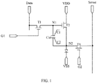
- FIG. 1 is an equivalent circuit diagram of a drive circuit, illustrating a 3T1 C drive circuit. As shown in FIG. 1 , the drive circuit is electrically connected to a first gate line G1, a sense line Sense, a power supply line VDD, a data line Data and a second gate line G2, and the drive circuit includes a switch transistor T1, a drive transistor T2, a sense transistor T3 and a storage capacitor Cst.
- a gate electrode of the switch transistor T1 is connected to the first gate line G1, a first electrode of the switch transistor T1 is connected to a node N1, and a second electrode of the switch transistor T1 is connected to the data line Data.
- a gate electrode of drive transistor T2 is connected to the node N1, a first electrode of the drive transistor T2 is connected to a node N2, and a second electrode of the drive transistor T2 is connected to the power supply line VDD.
- a gate electrode of the sense transistor T3 is connected to the second gate line G2, a first electrode of the sense transistor T3 is connected to the node N2, a second electrode of the sense transistor T3 is connected to the sense line Sense.
- An anode of a light emitting element OLED is connected to the node N2, a cathode of the light emitting element OLED is connected to the low power supply line VSS, and the light emitting element OLED is configured to emit light with corresponding brightness in response to a current of the first electrode of the drive transistor.
- the drive circuit turns on the switch transistor T1 through the first gate line G1, a data voltage Vdata provided by the data line Data is stored in the storage capacitor Cst via the switch transistor T1, thereby controlling the drive transistor T2 to generate current and to further drive the organic light emitting diode (OLED) to emit light.
- the sense transistor T3 may extract a threshold voltage Vth and a mobility of the drive transistor T2 in response to sensing timing, and the storage capacitor Cst is configured to maintain a voltage difference between the node N1 and the node N2 in one frame of a light emission period.
- the first electrode refers to a source electrode and the second electrode refers to a drain electrode.
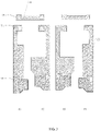
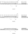
- FIG. 2A is a side view of a display substrate according to an embodiment of the present disclosure
- FIG. 2B is another side view of a display substrate according to an embodiment of the present disclosure.
- the display substrate according to this embodiment of the present disclosure includes a base substrate 10 and multiple sub-pixels disposed on the base substrate 10, wherein each sub-pixel includes a light-emitting region AA and a non-light-emitting region NA, and each sub-pixel is provided therein with a drive circuit.
- the drive circuit includes a storage capacitor Cst and multiple transistors, and the multiple transistors include a switch transistor T1, a drive transistor T2 and a sense transistor T3.
- the sub-pixels are disposed on the substrate in an array.
- a sub-pixel is taken as an example in FIG. 2A and FIG. 2B , both of FIG. 2A and FIG. 2B are side views from different perspectives.
- the base substrate 10 may be a rigid substrate or a flexible substrate, wherein the rigid substrate may be, but is not limited to, one or more of glass and metal foils; and the flexible substrate may be, but is not limited to, one or more of polyethylene glycol terephthalate, ethylene terephthalate, polyether ether ketone, polystyrene, polycarbonate, polyarylate, polyarylester, polyimide, polyvinyl chloride, polyethylene, and textile fibers.
- the rigid substrate may be, but is not limited to, one or more of glass and metal foils
- the flexible substrate may be, but is not limited to, one or more of polyethylene glycol terephthalate, ethylene terephthalate, polyether ether ketone, polystyrene, polycarbonate, polyarylate, polyarylester, polyimide, polyvinyl chloride, polyethylene, and textile fibers.
- the switch transistor T1 in the embodiment of the present disclosure includes an active layer 31, a gate electrode 32, a first electrode 33 and a second electrode 34 which are sequentially disposed on the base substrate 10.
- the drive transistor T2 includes an active layer 21, a gate electrode 22, a first electrode 23 and a second electrode 24 which are sequentially disposed on the base substrate 10.
- the sense transistor T3 includes an active layer 41, a gate electrode 42, a first electrode 43 and a second electrode 44 which are sequentially disposed on the base substrate 10.
- the display substrate according to the embodiment of the present disclosure is a bottom emission OLED display substrate.
- the storage capacitor in the embodiment of the present disclosure is a transparent capacitor, which does not affect light emitting effect of the display substrate and may ensure smooth light emitting.
- each sub-pixel is further provided with a light emitting element, which may be an OLED.
- a first electrode of the storage capacitor is disposed in a same layer as an active layer of the multiple transistors, but in a different layer from the source and drain electrodes of the multiple transistors, and a second electrode of the storage capacitor is on a side of the first electrode close to the substrate.
- a first electrode of the drive transistor is connected to the second electrode through an active layer of the drive transistor, and a first electrode of the sense transistor is connected to the second electrode through an active layer of the sense transistor.
- an active layer of each transistor includes a channel region A1, a first conductive region A2 and a second conductive region A3.
- the first conductive region A2 and the second conductive region A3 are respectively disposed on two sides of the channel region A1, wherein a second electrode of the transistor is connected to the first conductive region A2, and a first electrode of the transistor is connected to the second conductive region A3.
- the second conductive region A3 of the drive transistor T2 is connected to the second electrode C2, and the second conductive region A3 of the sense transistor T3 is connected to the second electrode C2.
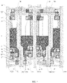
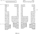
- FIG. 3 is a top view of the display substrate according to the embodiment of the present disclosure.
- the display substrate according to the embodiment of the present disclosure further includes a buffer layer 12 disposed on a side of an active layer of the transistor close to the base substrate 10, wherein the buffer layer 12 includes a first via hole V1 and a second via hole V2 exposing the second electrode C2.
- the second conductive region A3 of the drive transistor T2 is connected to the second electrode C2 through the first via hole V1
- the second conductive region A3 of the sense transistor T3 is connected to the second electrode C2 through the second via hole V2.
- the drive transistor T2 according to the embodiment of the present disclosure further includes a light shield layer 11 disposed on a side of the buffer layer 12 close to the base substrate 10.
- the light shield layer 11 is disposed on a side of the second electrode C2 close to the base substrate 10, or the second electrode C2 is disposed on a side of the light shield layer 11 close to the base substrate 10, wherein the light shield layer 11 disposed on the side of the second electrode C2 close to the base substrate 10 is taken as an example in FIG. 2 .
- the second conductive region A2 of the drive transistor T2 and the second conductive region A2 of the sense transistor T3 are connected to the second electrode C2 through the light shield layer 11.
- the surface of the light shield layer 11 close to the second electrode C2 is completely in contact with the second electrode C2 to avoid disposing an insulating layer between the light shield layer and the second electrode, which not only reduces the number of layers and thickness of the display substrate, but also reduces the number of use of masks, simplifies the manufacturing process and reduces manufacturing costs of the display substrate.
- the orthographic projection of the light shield layer 11 on the base substrate 10 covers an orthographic projection of the channel region A1 of the active layer 31 of the drive transistor T2 on the base substrate 10.
- the first gate line G1 and the second gate line G2 are disposed in a same layer as a gate electrode of a transistor, and a data line Data is disposed in a same layer as source and drain electrodes of the transistor.
- a first electrode C1 is respectively connected to a first electrode 33 of a switch transistor T1 and a gate electrode 22 of a drive transistor T2, and a second electrode C2 is respectively connected to a first electrode 23 of the drive transistor T2 and a first electrode 43 of a sense transistor T3.
- the gate electrode 22 of a switch transistor T1 is connected to the first gate line G1 among the gate lines corresponding to the sub-pixel
- a second electrode 34 of the switch transistor T1 is connected to the data line Data corresponding to the sub-pixel
- a gate electrode of the sense transistor T3 is connected to the second gate line G2 among the gate lines corresponding to the sub-pixel.
- a non-light-emitting region for each sub-pixel, includes a first non-light-emitting region and a second non-light-emitting region, wherein the first non-light-emitting region and the second non-light-emitting region are on two sides of the light-emitting region AA and disposed along an extending direction of the data line Data.
- the sense transistor T3 and the second gate line G2 are all in the first non-light-emitting region, and the switch transistor T1, the drive transistor T2 and the first gate line G1 are all in the second non-light-emitting region.
- the display substrate further includes a power supply line VDD and a sense line Sense which are disposed in a same layer as the data line Data.
- Each pixel includes four sub-pixels disposed along an extending direction of the gate lines, and each pixel corresponds to two columns of power supply lines and one column of sense line.
- pixel structures of a second sub-pixel and a third sub-pixel are symmetrically disposed, and a first sub-pixel and a fourth sub-pixel are symmetrically disposed.
- the sense line Sense corresponding to the pixel is located between the second sub-pixel P2 and the third sub-pixel P3, one column of power supply line VDD corresponding to the pixel is on a side of the first sub-pixel P1 away from the second sub-pixel P2, and another column of power supply line VDD corresponding to the pixel is on a side of the fourth sub-pixel P4 away from the third sub-pixel P3.
- a data line Data corresponding to the first sub-pixel P1 is on a side of the first sub-pixel P1 close to the second sub-pixel P2.
- a data line corresponding to the second sub-pixel P2 is on a side of the second sub-pixel P2 close to the first sub-pixel P1.
- a data line corresponding to the third sub-pixel P3 is on a side of the third sub-pixel P3 close to the fourth sub-pixel P4, and a data line corresponding to the fourth sub-pixel P4 is on a side of the fourth sub-pixel P4 close to the third sub-pixel P3.
- a second electrode of a drive transistor of the second sub-pixel P2 is connected to a power supply connection line VL.
- a second electrode of a drive transistor of the third sub-pixel P3 is connected to another power supply connection line VL.
- a second electrode of a sense transistor of the first sub-pixel P1 is connected to a sensing connection line SL through an active layer of the sense transistor.
- a second electrode of a sense transistor of the fourth sub-pixel P4 is connected to another sensing connection line SL through an active layer of the sense transistor.
- a sensing connection line SL may have a single-layer structure or a double-layer structure.
- the sensing connection line SL When the sensing connection line SL has a single-layer structure, it is disposed in a same layer as a light shield layer or a second electrode.
- a sensing connection line SL When a sensing connection line SL has a double-layer structure, a first layer of the sensing connection line is disposed in a same layer as the light shield layer, and a second layer of the sensing connection line is disposed in a same layer as the second electrode.
- the sensing connection line and the light shield layer disposed in the same layer are taken as an example in FIG. 3 .
- the interlayer insulating layer 14 is provided with a via hole exposing a conductive region of the active layer, and the source and drain electrodes of multiple transistors are connected to the conductive region of the active layer through the via hole.
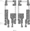
- FIG. 5 is a schematic diagram of local structure replacement according to an embodiment of the present disclosure.
- an interlayer insulating layer 14 in a display substrate according to the embodiment of the present disclosure includes a via hole V, wherein the via hole V is on a second side of a light-emitting region and exposes a gate electrode 22 and a first electrode C1 of a drive transistor at the same time.
- a first electrode 33 of a switch transistor T1 is connected to the gate electrode 22 and the first electrode C1 of the drive transistor T2 through the via hole V.
- the via hole V is a semi-buried hole, and the via hole V on the interlayer insulating layer may be made by a halftone mask.
- the first electrode C1 is made of a conductive active layer, which includes a transparent metal oxide and the transparent metal oxide includes Indium Gallium Zinc Oxide (abbreviated as IGZO), etc., which is not limited in the embodiments of the present disclosure.
- IGZO Indium Gallium Zinc Oxide
- an orthographic projection of the light emitting element on the base substrate 10 coincides with a light-emitting region AA, and the filter 50 is in the light-emitting region AA and disposed on a side of the light emitting element close to the base substrate 10.
- An orthographic projection of the anode 61 on the base substrate 10 covers an orthographic projection of the filter 50 on the base substrate 10.
- the display substrate according to the embodiment of the present disclosure further includes a passivation layer 15 disposed on a side of source and drain electrodes of the transistor away from the base substrate 10, a flat layer 16 disposed between the anode 61 and the filter 50, and a pixel defining layer 17 disposed on a side of the flat layer 16 away from the base substrate 10 for defining a sub-pixel region.
- the passivation layer 15 is disposed on a side of the filter 50 close to the base substrate 10, and the flat layer 16 is disposed between the light emitting element and the filter 50.
- the passivation layer 16 is provided with a fourth via hole V4 exposing the first electrode 43 of the sense transistor T3, and the flat layer 16 is provided with a fifth via hole V5 exposing the fourth via hole V4.
- the anode 61 is connected to the first electrode 43 of the sense transistor T3 through the fourth via hole V4 and the fifth via hole V5.
- An orthogonal projection of the fifth via hole V5 on the base substrate 10 does not completely coincide with an orthogonal projection of the second via hole V2 on the base substrate 10.
- the display substrate according to the embodiment of the present disclosure further includes a supporting part 70 disposed on a side of the light emitting element away from the base substrate 10 and a cover plate 80 disposed on a side of the supporting part 70 away from the base substrate 10.
- the cover plate 80 is configured to protect the light emitting elements, wherein the cover plate 80 may be a glass cover plate.
- an embodiment of the present disclosure further provides a display apparatus, including a display substrate.
- the display apparatus may be any product or component with a display function such as a mobile phone, a tablet computer, a television, a display, a laptop computer, a digital photo frame, a navigator, etc.
- a display function such as a mobile phone, a tablet computer, a television, a display, a laptop computer, a digital photo frame, a navigator, etc.
- Other essential components of the display apparatus is well known to those of ordinary skill in the art, which will not be described in detail here, and should not be taken as a limitation on the present disclosure.
- the implementation of the display apparatus may refer to the embodiment of the embedded touch screen described above, and the repetition will not be described in detail here.
- the display substrate is the display substrate provided in the preceding embodiments, and has similar implementation principles and implementation effects, which will not be described further here.
- FIG. 8 is a flowchart of the method for manufacturing a display substrate according to an embodiment of the present disclosure. As shown in FIG. 8 , the method for manufacturing a display substrate according to the embodiment of the present disclosure includes the following steps:
- each sub-pixel includes a light-emitting region and a non-light-emitting region, and each sub-pixel is provided with a drive circuit.
- the drive circuit includes a storage capacitor and multiple transistors.
- the multiple transistors include a switch transistor, a drive transistor and a sense transistor.
- the multiple transistors are in the non-light-emitting region, the storage capacitor is a transparent capacitor, and an orthographic projection of the storage capacitor on the base substrate coincides with the light-emitting region.
- a first electrode of the storage capacitor is disposed in a same layer as active layers of the multiple transistors, and a second electrode of the storage capacitor is on a side of the first electrode close to the base substrate.
- a first electrode of the drive transistor is connected to the second electrode through an active layer of the drive transistor, and a first electrode of the sense transistor is connected to the second electrode through an active layer of the sense transistor.
- the display substrate is the display substrate provided in the preceding embodiments, and has similar implementation principles and implementation effects, which will not be described further here.
- the display substrate further includes gate lines, data lines, power supply lines and sense lines, wherein the gate lines include a first gate line and a second gate line, and step S2 specifically includes forming a light shield layer and the second electrode on the base substrate; forming a first electrode and active layers of the multiple transistors on the light shield layer and the second electrode; forming gate electrodes of the multiple transistors, the first gate line and the second gate line on the first electrode and the active layers of the multiple transistors; forming the data lines, the power supply lines, the sense lines and source and drain electrodes of the multiple transistors on the gate electrodes of the transistors, the first gate line and the second gate line; sequentially forming filters and light emitting elements on the data lines, the power supply lines, the sense lines and the source and drain electrodes of the multiple transistors.
- sequentially forming the light shield layer and the second electrode on the base substrate includes forming the light shield layer on the base substrate using a first mask and forming the second electrode on the light shield layer using a second mask.
- sequentially forming the second electrode and the light shield layer on the base substrate includes forming the second electrode on the base substrate using the second mask by a patterning process and forming the light shield layer on the second electrode using the first mask.
- simultaneously forming the second electrode and the light shield layer on the base substrate includes sequentially depositing a shading thin film and a transparent conductive thin film on the base substrate, and simultaneously forming the second electrode and the light shield layer using a halftone mask.
- the patterning process includes: photoresist coating, exposure, development, etching, photoresist stripping, etc.
- forming the first electrode and the active layers of the multiple transistors on the light shield layer and the second electrode includes forming a buffer layer including a first via hole, a second via hole and a third via hole on the light shield layer and the second electrode; the first via hole and the second via hole exposing the second electrode, and the third via hole exposing a sensing connection line; forming the first electrode and the active layers of the multiple transistors on the buffer layer using a same manufacturing process.
- sequentially forming the filters and the light emitting elements on the data lines, the power supply lines, the sense lines and the source and drain electrodes of the multiple transistors includes forming a passivation layer including a fourth via hole on the data lines, the power supply lines, the sense lines and the source and drain electrodes of the multiple transistors; the fourth via hole exposing the first electrode of the sense transistor; sequentially forming an filter and a flat layer including a fifth via hole on the passivation layer; the fifth via hole exposing a seventh via hole; forming the light emitting elements on the flat layer.
- FIGS. 9a-9F which includes the following steps:
- forming the first electrode and the active layers of the multiple transistors on the light shield layer and the second electrode includes forming a buffer layer including a first via hole, a second via hole and a third via hole on the light shield layer and the second electrode; forming the first electrode and the active layers of the multiple transistors on the buffer layer using the same manufacturing process.
- the first via hole and the second via hole expose the second electrode, and the third via hole exposes a sensing connection line.
- the sensing connection line has a single-layer structure and is disposed in a same layer as a light shield layer, and the light shield layer is disposed on a side of the second electrode close to the base substrate
- a method for manufacturing a display substrate according to an embodiment of the present disclosure will be further explained with reference to FIGS. 10 to 16 , the method includes the following steps:
Landscapes
- Engineering & Computer Science (AREA)
- Microelectronics & Electronic Packaging (AREA)
- Physics & Mathematics (AREA)
- Geometry (AREA)
- Devices For Indicating Variable Information By Combining Individual Elements (AREA)
- Electroluminescent Light Sources (AREA)
- Thin Film Transistor (AREA)
Applications Claiming Priority (2)
| Application Number | Priority Date | Filing Date | Title |
|---|---|---|---|
| CN201911038817.7A CN112750861B (zh) | 2019-10-29 | 2019-10-29 | 一种显示基板及其制作方法、显示装置 |
| PCT/CN2020/109999 WO2021082648A1 (zh) | 2019-10-29 | 2020-08-19 | 一种显示基板及其制作方法、显示装置 |
Publications (3)
| Publication Number | Publication Date |
|---|---|
| EP4053904A1 true EP4053904A1 (de) | 2022-09-07 |
| EP4053904A4 EP4053904A4 (de) | 2022-12-14 |
| EP4053904B1 EP4053904B1 (de) | 2024-04-24 |
Family
ID=75641637
Family Applications (1)
| Application Number | Title | Priority Date | Filing Date |
|---|---|---|---|
| EP20870454.4A Active EP4053904B1 (de) | 2019-10-29 | 2020-08-19 | Anzeigesubstrat, herstellungsverfahren dafür und anzeigevorrichtung |
Country Status (5)
| Country | Link |
|---|---|
| US (1) | US12232363B2 (de) |
| EP (1) | EP4053904B1 (de) |
| JP (1) | JP7577074B2 (de) |
| CN (1) | CN112750861B (de) |
| WO (1) | WO2021082648A1 (de) |
Families Citing this family (20)
| Publication number | Priority date | Publication date | Assignee | Title |
|---|---|---|---|---|
| KR20210116760A (ko) * | 2020-03-13 | 2021-09-28 | 삼성디스플레이 주식회사 | 표시 장치 |
| CN112968034A (zh) * | 2021-02-24 | 2021-06-15 | 合肥鑫晟光电科技有限公司 | 显示面板及其制作方法和显示装置 |
| CN113299747A (zh) | 2021-05-21 | 2021-08-24 | 合肥京东方卓印科技有限公司 | 显示面板及其制作方法和显示装置 |
| CN113394236B (zh) * | 2021-05-28 | 2024-04-09 | 武汉天马微电子有限公司 | 显示面板及显示装置 |
| CN113471221B (zh) * | 2021-07-01 | 2024-05-14 | 京东方科技集团股份有限公司 | 一种显示面板、制备方法及显示装置 |
| GB2618939A (en) * | 2021-07-12 | 2023-11-22 | Boe Technology Group Co Ltd | Display substrate and preparation method therefor, and display device |
| CN113594220B (zh) * | 2021-07-30 | 2024-05-14 | 京东方科技集团股份有限公司 | 显示基板及其测试方法、制备方法、显示装置 |
| CN115911050A (zh) * | 2021-09-29 | 2023-04-04 | 京东方科技集团股份有限公司 | 显示基板及其制备方法、显示装置 |
| CN113972223B (zh) * | 2021-10-21 | 2026-03-06 | 京东方科技集团股份有限公司 | 显示基板和显示装置 |
| CN114242755B (zh) * | 2021-11-24 | 2025-07-04 | 合肥京东方卓印科技有限公司 | 显示基板及显示装置 |
| CN114203631B (zh) * | 2021-12-10 | 2024-12-27 | Tcl华星光电技术有限公司 | 显示面板的制造方法以及显示面板 |
| CN114784015B (zh) * | 2022-03-28 | 2025-09-19 | 京东方科技集团股份有限公司 | 一种显示基板、其制作方法、驱动方法及显示装置 |
| DE112022007112T5 (de) * | 2022-04-28 | 2025-03-06 | Boe Technology Group Co., Ltd. | Anzeigefeld und anzeigevorrichtung |
| US20230371310A1 (en) * | 2022-05-16 | 2023-11-16 | Samsung Display Co., Ltd. | Display apparatus and method of manufacturing the same |
| CN115440747B (zh) * | 2022-10-18 | 2024-11-15 | 京东方科技集团股份有限公司 | 显示基板及其制备方法、显示装置 |
| KR20240118968A (ko) * | 2023-01-27 | 2024-08-06 | 삼성디스플레이 주식회사 | 표시 장치 |
| CN120604657A (zh) * | 2024-01-03 | 2025-09-05 | 京东方科技集团股份有限公司 | 阵列基板、显示面板及显示装置 |
| CN118265365A (zh) * | 2024-03-29 | 2024-06-28 | 京东方科技集团股份有限公司 | 显示基板及显示装置 |
| CN118475172A (zh) * | 2024-05-23 | 2024-08-09 | 京东方科技集团股份有限公司 | 驱动背板、显示面板及显示装置 |
| WO2026000176A1 (en) * | 2024-06-25 | 2026-01-02 | Boe Technology Group Co., Ltd. | Array substrate, display apparatus, and method of fabricating array substrate |
Family Cites Families (24)
| Publication number | Priority date | Publication date | Assignee | Title |
|---|---|---|---|---|
| CN103904086B (zh) * | 2012-12-24 | 2017-10-27 | 上海天马微电子有限公司 | 一种薄膜晶体管阵列基板 |
| US9911799B2 (en) * | 2013-05-22 | 2018-03-06 | Samsung Display Co., Ltd. | Organic light-emitting display apparatus and method of repairing the same |
| US9583516B2 (en) | 2013-10-25 | 2017-02-28 | Semiconductor Energy Laboratory Co., Ltd. | Display device |
| KR102124025B1 (ko) | 2013-12-23 | 2020-06-17 | 엘지디스플레이 주식회사 | 유기발광다이오드 표시장치 및 그 제조방법 |
| KR102542177B1 (ko) * | 2016-03-15 | 2023-06-13 | 삼성디스플레이 주식회사 | 유기 발광 표시 장치 및 이를 구비한 전자 기기 |
| KR102675913B1 (ko) | 2016-04-29 | 2024-06-17 | 엘지디스플레이 주식회사 | 백플레인 기판 및 이를 이용한 유기 발광 표시 장치 |
| CN112038358A (zh) * | 2016-05-17 | 2020-12-04 | 群创光电股份有限公司 | 显示设备 |
| TWI607562B (zh) | 2016-07-11 | 2017-12-01 | 友達光電股份有限公司 | 顯示面板 |
| KR102600693B1 (ko) * | 2016-09-21 | 2023-11-09 | 엘지디스플레이 주식회사 | 박막 트랜지스터 어레이 기판 및 그의 제조방법 |
| KR101849590B1 (ko) * | 2016-10-31 | 2018-05-31 | 엘지디스플레이 주식회사 | 유기 발광 표시 장치 및 그 제조 방법 |
| KR102662278B1 (ko) * | 2016-11-30 | 2024-05-02 | 엘지디스플레이 주식회사 | 유기 발광 표시 장치 및 그 제조 방법 |
| KR102792467B1 (ko) | 2016-12-26 | 2025-04-08 | 엘지디스플레이 주식회사 | 표시 장치 |
| KR102431929B1 (ko) | 2017-10-31 | 2022-08-12 | 엘지디스플레이 주식회사 | 표시장치 및 그 제조방법 |
| KR102615707B1 (ko) | 2017-12-29 | 2023-12-18 | 엘지디스플레이 주식회사 | 유기발광표시패널 및 이를 이용한 유기발광표시장치 |
| CN108461529A (zh) * | 2018-03-29 | 2018-08-28 | 京东方科技集团股份有限公司 | 一种阵列基板及其制备方法、显示装置 |
| CN108428730B (zh) | 2018-05-16 | 2021-01-26 | 京东方科技集团股份有限公司 | Oled显示基板及其制作方法、显示装置 |
| CN108767016B (zh) * | 2018-05-21 | 2021-09-21 | 京东方科技集团股份有限公司 | 一种薄膜晶体管及其制作方法、阵列基板、显示装置 |
| CN108735792B (zh) * | 2018-08-14 | 2020-07-31 | 京东方科技集团股份有限公司 | 底发射型oled阵列基板及其制作方法、显示面板、显示装置 |
| CN109036291B (zh) | 2018-09-18 | 2020-11-10 | 京东方科技集团股份有限公司 | 一种显示面板及其控制方法、显示装置 |
| KR102654918B1 (ko) * | 2018-10-08 | 2024-04-05 | 삼성디스플레이 주식회사 | 표시장치 |
| KR102675918B1 (ko) * | 2018-10-24 | 2024-06-17 | 엘지디스플레이 주식회사 | 스토리지 캐패시터, 이를 이용한 표시 장치 및 이의 제조 방법 |
| CN109742113B (zh) * | 2019-01-08 | 2020-12-25 | 京东方科技集团股份有限公司 | 一种阵列基板、其制备方法及相关装置 |
| KR102837373B1 (ko) * | 2019-08-19 | 2025-07-23 | 삼성디스플레이 주식회사 | 표시 장치 |
| CN112750859B (zh) * | 2019-10-29 | 2022-07-29 | 京东方科技集团股份有限公司 | 一种显示基板及其制作方法、显示装置 |
-
2019
- 2019-10-29 CN CN201911038817.7A patent/CN112750861B/zh active Active
-
2020
- 2020-08-19 JP JP2021563681A patent/JP7577074B2/ja active Active
- 2020-08-19 WO PCT/CN2020/109999 patent/WO2021082648A1/zh not_active Ceased
- 2020-08-19 US US17/281,266 patent/US12232363B2/en active Active
- 2020-08-19 EP EP20870454.4A patent/EP4053904B1/de active Active
Also Published As
| Publication number | Publication date |
|---|---|
| EP4053904A4 (de) | 2022-12-14 |
| WO2021082648A1 (zh) | 2021-05-06 |
| WO2021082648A9 (zh) | 2022-05-19 |
| CN112750861A (zh) | 2021-05-04 |
| EP4053904B1 (de) | 2024-04-24 |
| JP2023501842A (ja) | 2023-01-20 |
| US12232363B2 (en) | 2025-02-18 |
| JP7577074B2 (ja) | 2024-11-01 |
| US20220013612A1 (en) | 2022-01-13 |
| CN112750861B (zh) | 2025-02-25 |
Similar Documents
| Publication | Publication Date | Title |
|---|---|---|
| US12232363B2 (en) | Display substrate, manufacturing method thereof, and display apparatus | |
| US12426365B2 (en) | Display substrate and manufacturing method therefor, and display device | |
| EP3992705B1 (de) | Anzeigesubstrat und anzeigevorrichtung | |
| KR102443121B1 (ko) | 디스플레이 패널 및 그 제조 방법 및 디스플레이 디바이스 | |
| US9088003B2 (en) | Reducing sheet resistance for common electrode in top emission organic light emitting diode display | |
| US12317687B2 (en) | Display substrate and preparation method thereof, and display apparatus | |
| US12230215B2 (en) | Display substrate, manufacturing method therefor, and display apparatus | |
| US12439692B2 (en) | Display substrate, manufacturing method therefor, and display apparatus | |
| JP2013161895A (ja) | 薄膜トランジスタ、表示装置および電子機器 | |
| US12236855B2 (en) | Pixel circuit, driving method thereof, and display apparatus | |
| WO2022042041A1 (zh) | 显示基板、显示装置 | |
| US20250017089A1 (en) | Display Panel, Manufacturing Method Therefor, and Display Device | |
| US12262608B2 (en) | Display substrate having bezel region at periphery of first display region and second display region and preparation method thereof, and display apparatus having the same | |
| US20230026444A1 (en) | Display device and driving method therefor | |
| US20240121997A1 (en) | Display Substrate, Preparation Method Thereof, and Display Apparatus | |
| CN115835730B (zh) | 显示基板以及显示装置 | |
| US20240397763A1 (en) | Display Substrate, Manufacturing Method Therefor, and Display Apparatus | |
| US12579937B2 (en) | Display substrate and driving method therefor, and display apparatus, driving apparatus and medium | |
| CN223322383U (zh) | 显示基板和显示装置 | |
| US20250248245A1 (en) | Display Substrate, Preparation Method therefor, and Display Apparatus | |
| WO2023230915A1 (zh) | 显示基板以及显示装置 | |
| WO2023230919A1 (zh) | 显示基板以及显示装置 |
Legal Events
| Date | Code | Title | Description |
|---|---|---|---|
| STAA | Information on the status of an ep patent application or granted ep patent |
Free format text: STATUS: UNKNOWN |
|
| STAA | Information on the status of an ep patent application or granted ep patent |
Free format text: STATUS: THE INTERNATIONAL PUBLICATION HAS BEEN MADE |
|
| PUAI | Public reference made under article 153(3) epc to a published international application that has entered the european phase |
Free format text: ORIGINAL CODE: 0009012 |
|
| STAA | Information on the status of an ep patent application or granted ep patent |
Free format text: STATUS: REQUEST FOR EXAMINATION WAS MADE |
|
| 17P | Request for examination filed |
Effective date: 20210408 |
|
| AK | Designated contracting states |
Kind code of ref document: A1 Designated state(s): AL AT BE BG CH CY CZ DE DK EE ES FI FR GB GR HR HU IE IS IT LI LT LU LV MC MK MT NL NO PL PT RO RS SE SI SK SM TR |
|
| A4 | Supplementary search report drawn up and despatched |
Effective date: 20221115 |
|
| RIC1 | Information provided on ipc code assigned before grant |
Ipc: H01L 21/82 20060101ALI20221109BHEP Ipc: H01L 21/77 20170101ALI20221109BHEP Ipc: H01L 27/32 20060101AFI20221109BHEP |
|
| DAV | Request for validation of the european patent (deleted) | ||
| DAX | Request for extension of the european patent (deleted) | ||
| STAA | Information on the status of an ep patent application or granted ep patent |
Free format text: STATUS: EXAMINATION IS IN PROGRESS |
|
| 17Q | First examination report despatched |
Effective date: 20230602 |
|
| REG | Reference to a national code |
Ref country code: DE Ref legal event code: R079 Free format text: PREVIOUS MAIN CLASS: H01L0027320000 Ipc: H10K0059121000 Ref document number: 602020029793 Country of ref document: DE |
|
| GRAP | Despatch of communication of intention to grant a patent |
Free format text: ORIGINAL CODE: EPIDOSNIGR1 |
|
| STAA | Information on the status of an ep patent application or granted ep patent |
Free format text: STATUS: GRANT OF PATENT IS INTENDED |
|
| RIC1 | Information provided on ipc code assigned before grant |
Ipc: H10K 59/126 20230101ALI20231123BHEP Ipc: H10K 59/121 20230101AFI20231123BHEP |
|
| INTG | Intention to grant announced |
Effective date: 20231218 |
|
| GRAS | Grant fee paid |
Free format text: ORIGINAL CODE: EPIDOSNIGR3 |
|
| GRAA | (expected) grant |
Free format text: ORIGINAL CODE: 0009210 |
|
| STAA | Information on the status of an ep patent application or granted ep patent |
Free format text: STATUS: THE PATENT HAS BEEN GRANTED |
|
| AK | Designated contracting states |
Kind code of ref document: B1 Designated state(s): AL AT BE BG CH CY CZ DE DK EE ES FI FR GB GR HR HU IE IS IT LI LT LU LV MC MK MT NL NO PL PT RO RS SE SI SK SM TR |
|
| REG | Reference to a national code |
Ref country code: GB Ref legal event code: FG4D |
|
| REG | Reference to a national code |
Ref country code: CH Ref legal event code: EP |
|
| REG | Reference to a national code |
Ref country code: DE Ref legal event code: R096 Ref document number: 602020029793 Country of ref document: DE |
|
| REG | Reference to a national code |
Ref country code: IE Ref legal event code: FG4D |
|
| REG | Reference to a national code |
Ref country code: LT Ref legal event code: MG9D |
|
| REG | Reference to a national code |
Ref country code: NL Ref legal event code: MP Effective date: 20240424 |
|
| REG | Reference to a national code |
Ref country code: AT Ref legal event code: MK05 Ref document number: 1681016 Country of ref document: AT Kind code of ref document: T Effective date: 20240424 |
|
| PG25 | Lapsed in a contracting state [announced via postgrant information from national office to epo] |
Ref country code: NL Free format text: LAPSE BECAUSE OF FAILURE TO SUBMIT A TRANSLATION OF THE DESCRIPTION OR TO PAY THE FEE WITHIN THE PRESCRIBED TIME-LIMIT Effective date: 20240424 |
|
| PG25 | Lapsed in a contracting state [announced via postgrant information from national office to epo] |
Ref country code: NL Free format text: LAPSE BECAUSE OF FAILURE TO SUBMIT A TRANSLATION OF THE DESCRIPTION OR TO PAY THE FEE WITHIN THE PRESCRIBED TIME-LIMIT Effective date: 20240424 |
|
| PG25 | Lapsed in a contracting state [announced via postgrant information from national office to epo] |
Ref country code: IS Free format text: LAPSE BECAUSE OF FAILURE TO SUBMIT A TRANSLATION OF THE DESCRIPTION OR TO PAY THE FEE WITHIN THE PRESCRIBED TIME-LIMIT Effective date: 20240824 |
|
| PG25 | Lapsed in a contracting state [announced via postgrant information from national office to epo] |
Ref country code: BG Free format text: LAPSE BECAUSE OF FAILURE TO SUBMIT A TRANSLATION OF THE DESCRIPTION OR TO PAY THE FEE WITHIN THE PRESCRIBED TIME-LIMIT Effective date: 20240424 |
|
| PG25 | Lapsed in a contracting state [announced via postgrant information from national office to epo] |
Ref country code: HR Free format text: LAPSE BECAUSE OF FAILURE TO SUBMIT A TRANSLATION OF THE DESCRIPTION OR TO PAY THE FEE WITHIN THE PRESCRIBED TIME-LIMIT Effective date: 20240424 Ref country code: FI Free format text: LAPSE BECAUSE OF FAILURE TO SUBMIT A TRANSLATION OF THE DESCRIPTION OR TO PAY THE FEE WITHIN THE PRESCRIBED TIME-LIMIT Effective date: 20240424 |
|
| PG25 | Lapsed in a contracting state [announced via postgrant information from national office to epo] |
Ref country code: GR Free format text: LAPSE BECAUSE OF FAILURE TO SUBMIT A TRANSLATION OF THE DESCRIPTION OR TO PAY THE FEE WITHIN THE PRESCRIBED TIME-LIMIT Effective date: 20240725 |
|
| PG25 | Lapsed in a contracting state [announced via postgrant information from national office to epo] |
Ref country code: PT Free format text: LAPSE BECAUSE OF FAILURE TO SUBMIT A TRANSLATION OF THE DESCRIPTION OR TO PAY THE FEE WITHIN THE PRESCRIBED TIME-LIMIT Effective date: 20240826 |
|
| PG25 | Lapsed in a contracting state [announced via postgrant information from national office to epo] |
Ref country code: ES Free format text: LAPSE BECAUSE OF FAILURE TO SUBMIT A TRANSLATION OF THE DESCRIPTION OR TO PAY THE FEE WITHIN THE PRESCRIBED TIME-LIMIT Effective date: 20240424 |
|
| PG25 | Lapsed in a contracting state [announced via postgrant information from national office to epo] |
Ref country code: AT Free format text: LAPSE BECAUSE OF FAILURE TO SUBMIT A TRANSLATION OF THE DESCRIPTION OR TO PAY THE FEE WITHIN THE PRESCRIBED TIME-LIMIT Effective date: 20240424 |
|
| PG25 | Lapsed in a contracting state [announced via postgrant information from national office to epo] |
Ref country code: PL Free format text: LAPSE BECAUSE OF FAILURE TO SUBMIT A TRANSLATION OF THE DESCRIPTION OR TO PAY THE FEE WITHIN THE PRESCRIBED TIME-LIMIT Effective date: 20240424 |
|
| PG25 | Lapsed in a contracting state [announced via postgrant information from national office to epo] |
Ref country code: LV Free format text: LAPSE BECAUSE OF FAILURE TO SUBMIT A TRANSLATION OF THE DESCRIPTION OR TO PAY THE FEE WITHIN THE PRESCRIBED TIME-LIMIT Effective date: 20240424 |
|
| PG25 | Lapsed in a contracting state [announced via postgrant information from national office to epo] |
Ref country code: PT Free format text: LAPSE BECAUSE OF FAILURE TO SUBMIT A TRANSLATION OF THE DESCRIPTION OR TO PAY THE FEE WITHIN THE PRESCRIBED TIME-LIMIT Effective date: 20240826 Ref country code: PL Free format text: LAPSE BECAUSE OF FAILURE TO SUBMIT A TRANSLATION OF THE DESCRIPTION OR TO PAY THE FEE WITHIN THE PRESCRIBED TIME-LIMIT Effective date: 20240424 Ref country code: NO Free format text: LAPSE BECAUSE OF FAILURE TO SUBMIT A TRANSLATION OF THE DESCRIPTION OR TO PAY THE FEE WITHIN THE PRESCRIBED TIME-LIMIT Effective date: 20240724 Ref country code: LV Free format text: LAPSE BECAUSE OF FAILURE TO SUBMIT A TRANSLATION OF THE DESCRIPTION OR TO PAY THE FEE WITHIN THE PRESCRIBED TIME-LIMIT Effective date: 20240424 Ref country code: IS Free format text: LAPSE BECAUSE OF FAILURE TO SUBMIT A TRANSLATION OF THE DESCRIPTION OR TO PAY THE FEE WITHIN THE PRESCRIBED TIME-LIMIT Effective date: 20240824 Ref country code: HR Free format text: LAPSE BECAUSE OF FAILURE TO SUBMIT A TRANSLATION OF THE DESCRIPTION OR TO PAY THE FEE WITHIN THE PRESCRIBED TIME-LIMIT Effective date: 20240424 Ref country code: GR Free format text: LAPSE BECAUSE OF FAILURE TO SUBMIT A TRANSLATION OF THE DESCRIPTION OR TO PAY THE FEE WITHIN THE PRESCRIBED TIME-LIMIT Effective date: 20240725 Ref country code: FI Free format text: LAPSE BECAUSE OF FAILURE TO SUBMIT A TRANSLATION OF THE DESCRIPTION OR TO PAY THE FEE WITHIN THE PRESCRIBED TIME-LIMIT Effective date: 20240424 Ref country code: ES Free format text: LAPSE BECAUSE OF FAILURE TO SUBMIT A TRANSLATION OF THE DESCRIPTION OR TO PAY THE FEE WITHIN THE PRESCRIBED TIME-LIMIT Effective date: 20240424 Ref country code: BG Free format text: LAPSE BECAUSE OF FAILURE TO SUBMIT A TRANSLATION OF THE DESCRIPTION OR TO PAY THE FEE WITHIN THE PRESCRIBED TIME-LIMIT Effective date: 20240424 Ref country code: AT Free format text: LAPSE BECAUSE OF FAILURE TO SUBMIT A TRANSLATION OF THE DESCRIPTION OR TO PAY THE FEE WITHIN THE PRESCRIBED TIME-LIMIT Effective date: 20240424 Ref country code: RS Free format text: LAPSE BECAUSE OF FAILURE TO SUBMIT A TRANSLATION OF THE DESCRIPTION OR TO PAY THE FEE WITHIN THE PRESCRIBED TIME-LIMIT Effective date: 20240724 |
|
| PG25 | Lapsed in a contracting state [announced via postgrant information from national office to epo] |
Ref country code: DK Free format text: LAPSE BECAUSE OF FAILURE TO SUBMIT A TRANSLATION OF THE DESCRIPTION OR TO PAY THE FEE WITHIN THE PRESCRIBED TIME-LIMIT Effective date: 20240424 |
|
| PG25 | Lapsed in a contracting state [announced via postgrant information from national office to epo] |
Ref country code: EE Free format text: LAPSE BECAUSE OF FAILURE TO SUBMIT A TRANSLATION OF THE DESCRIPTION OR TO PAY THE FEE WITHIN THE PRESCRIBED TIME-LIMIT Effective date: 20240424 |
|
| PG25 | Lapsed in a contracting state [announced via postgrant information from national office to epo] |
Ref country code: CZ Free format text: LAPSE BECAUSE OF FAILURE TO SUBMIT A TRANSLATION OF THE DESCRIPTION OR TO PAY THE FEE WITHIN THE PRESCRIBED TIME-LIMIT Effective date: 20240424 |
|
| PG25 | Lapsed in a contracting state [announced via postgrant information from national office to epo] |
Ref country code: SK Free format text: LAPSE BECAUSE OF FAILURE TO SUBMIT A TRANSLATION OF THE DESCRIPTION OR TO PAY THE FEE WITHIN THE PRESCRIBED TIME-LIMIT Effective date: 20240424 Ref country code: RO Free format text: LAPSE BECAUSE OF FAILURE TO SUBMIT A TRANSLATION OF THE DESCRIPTION OR TO PAY THE FEE WITHIN THE PRESCRIBED TIME-LIMIT Effective date: 20240424 |
|
| REG | Reference to a national code |
Ref country code: DE Ref legal event code: R097 Ref document number: 602020029793 Country of ref document: DE |
|
| PG25 | Lapsed in a contracting state [announced via postgrant information from national office to epo] |
Ref country code: SM Free format text: LAPSE BECAUSE OF FAILURE TO SUBMIT A TRANSLATION OF THE DESCRIPTION OR TO PAY THE FEE WITHIN THE PRESCRIBED TIME-LIMIT Effective date: 20240424 |
|
| PG25 | Lapsed in a contracting state [announced via postgrant information from national office to epo] |
Ref country code: SM Free format text: LAPSE BECAUSE OF FAILURE TO SUBMIT A TRANSLATION OF THE DESCRIPTION OR TO PAY THE FEE WITHIN THE PRESCRIBED TIME-LIMIT Effective date: 20240424 Ref country code: SK Free format text: LAPSE BECAUSE OF FAILURE TO SUBMIT A TRANSLATION OF THE DESCRIPTION OR TO PAY THE FEE WITHIN THE PRESCRIBED TIME-LIMIT Effective date: 20240424 Ref country code: RO Free format text: LAPSE BECAUSE OF FAILURE TO SUBMIT A TRANSLATION OF THE DESCRIPTION OR TO PAY THE FEE WITHIN THE PRESCRIBED TIME-LIMIT Effective date: 20240424 Ref country code: EE Free format text: LAPSE BECAUSE OF FAILURE TO SUBMIT A TRANSLATION OF THE DESCRIPTION OR TO PAY THE FEE WITHIN THE PRESCRIBED TIME-LIMIT Effective date: 20240424 Ref country code: DK Free format text: LAPSE BECAUSE OF FAILURE TO SUBMIT A TRANSLATION OF THE DESCRIPTION OR TO PAY THE FEE WITHIN THE PRESCRIBED TIME-LIMIT Effective date: 20240424 Ref country code: CZ Free format text: LAPSE BECAUSE OF FAILURE TO SUBMIT A TRANSLATION OF THE DESCRIPTION OR TO PAY THE FEE WITHIN THE PRESCRIBED TIME-LIMIT Effective date: 20240424 |
|
| PLBE | No opposition filed within time limit |
Free format text: ORIGINAL CODE: 0009261 |
|
| STAA | Information on the status of an ep patent application or granted ep patent |
Free format text: STATUS: NO OPPOSITION FILED WITHIN TIME LIMIT |
|
| REG | Reference to a national code |
Ref country code: CH Ref legal event code: PL |
|
| 26N | No opposition filed |
Effective date: 20250127 |
|
| PG25 | Lapsed in a contracting state [announced via postgrant information from national office to epo] |
Ref country code: LU Free format text: LAPSE BECAUSE OF NON-PAYMENT OF DUE FEES Effective date: 20240819 |
|
| PG25 | Lapsed in a contracting state [announced via postgrant information from national office to epo] |
Ref country code: SI Free format text: LAPSE BECAUSE OF FAILURE TO SUBMIT A TRANSLATION OF THE DESCRIPTION OR TO PAY THE FEE WITHIN THE PRESCRIBED TIME-LIMIT Effective date: 20240424 Ref country code: CH Free format text: LAPSE BECAUSE OF NON-PAYMENT OF DUE FEES Effective date: 20240831 Ref country code: MC Free format text: LAPSE BECAUSE OF FAILURE TO SUBMIT A TRANSLATION OF THE DESCRIPTION OR TO PAY THE FEE WITHIN THE PRESCRIBED TIME-LIMIT Effective date: 20240424 |
|
| REG | Reference to a national code |
Ref country code: BE Ref legal event code: MM Effective date: 20240831 |
|
| PG25 | Lapsed in a contracting state [announced via postgrant information from national office to epo] |
Ref country code: BE Free format text: LAPSE BECAUSE OF NON-PAYMENT OF DUE FEES Effective date: 20240831 |
|
| PG25 | Lapsed in a contracting state [announced via postgrant information from national office to epo] |
Ref country code: IE Free format text: LAPSE BECAUSE OF NON-PAYMENT OF DUE FEES Effective date: 20240819 |
|
| PG25 | Lapsed in a contracting state [announced via postgrant information from national office to epo] |
Ref country code: SE Free format text: LAPSE BECAUSE OF FAILURE TO SUBMIT A TRANSLATION OF THE DESCRIPTION OR TO PAY THE FEE WITHIN THE PRESCRIBED TIME-LIMIT Effective date: 20240424 |
|
| PGFP | Annual fee paid to national office [announced via postgrant information from national office to epo] |
Ref country code: DE Payment date: 20250820 Year of fee payment: 6 |
|
| PGFP | Annual fee paid to national office [announced via postgrant information from national office to epo] |
Ref country code: GB Payment date: 20250820 Year of fee payment: 6 |
|
| PGFP | Annual fee paid to national office [announced via postgrant information from national office to epo] |
Ref country code: FR Payment date: 20250828 Year of fee payment: 6 |
|
| PG25 | Lapsed in a contracting state [announced via postgrant information from national office to epo] |
Ref country code: IT Free format text: LAPSE BECAUSE OF FAILURE TO SUBMIT A TRANSLATION OF THE DESCRIPTION OR TO PAY THE FEE WITHIN THE PRESCRIBED TIME-LIMIT Effective date: 20240424 Ref country code: CY Free format text: LAPSE BECAUSE OF FAILURE TO SUBMIT A TRANSLATION OF THE DESCRIPTION OR TO PAY THE FEE WITHIN THE PRESCRIBED TIME-LIMIT; INVALID AB INITIO Effective date: 20200819 |
|
| PG25 | Lapsed in a contracting state [announced via postgrant information from national office to epo] |
Ref country code: HU Free format text: LAPSE BECAUSE OF FAILURE TO SUBMIT A TRANSLATION OF THE DESCRIPTION OR TO PAY THE FEE WITHIN THE PRESCRIBED TIME-LIMIT; INVALID AB INITIO Effective date: 20200819 |