EP4040301A2 - Verfahren und system zur seriellen unterbrechung einer sammelleitung mit niedriger pin-zahl (lpc) - Google Patents
Verfahren und system zur seriellen unterbrechung einer sammelleitung mit niedriger pin-zahl (lpc) Download PDFInfo
- Publication number
- EP4040301A2 EP4040301A2 EP22151504.2A EP22151504A EP4040301A2 EP 4040301 A2 EP4040301 A2 EP 4040301A2 EP 22151504 A EP22151504 A EP 22151504A EP 4040301 A2 EP4040301 A2 EP 4040301A2
- Authority
- EP
- European Patent Office
- Prior art keywords
- signal
- interrupt
- external device
- host
- inverter
- Prior art date
- Legal status (The legal status is an assumption and is not a legal conclusion. Google has not performed a legal analysis and makes no representation as to the accuracy of the status listed.)
- Granted
Links
Images






Classifications
-
- H—ELECTRICITY
- H03—ELECTRONIC CIRCUITRY
- H03K—PULSE TECHNIQUE
- H03K19/00—Logic circuits, i.e. having at least two inputs acting on one output; Inverting circuits
- H03K19/0175—Coupling arrangements; Interface arrangements
- H03K19/0185—Coupling arrangements; Interface arrangements using field effect transistors only
- H03K19/018507—Interface arrangements
- H03K19/018521—Interface arrangements of complementary type, e.g. CMOS
-
- G—PHYSICS
- G06—COMPUTING OR CALCULATING; COUNTING
- G06F—ELECTRIC DIGITAL DATA PROCESSING
- G06F13/00—Interconnection of, or transfer of information or other signals between, memories, input/output devices or central processing units
- G06F13/14—Handling requests for interconnection or transfer
- G06F13/20—Handling requests for interconnection or transfer for access to input/output bus
- G06F13/24—Handling requests for interconnection or transfer for access to input/output bus using interrupt
-
- G—PHYSICS
- G06—COMPUTING OR CALCULATING; COUNTING
- G06F—ELECTRIC DIGITAL DATA PROCESSING
- G06F13/00—Interconnection of, or transfer of information or other signals between, memories, input/output devices or central processing units
- G06F13/14—Handling requests for interconnection or transfer
- G06F13/20—Handling requests for interconnection or transfer for access to input/output bus
- G06F13/28—Handling requests for interconnection or transfer for access to input/output bus using burst mode transfer, e.g. direct memory access DMA, cycle steal
-
- G—PHYSICS
- G06—COMPUTING OR CALCULATING; COUNTING
- G06F—ELECTRIC DIGITAL DATA PROCESSING
- G06F13/00—Interconnection of, or transfer of information or other signals between, memories, input/output devices or central processing units
- G06F13/38—Information transfer, e.g. on bus
- G06F13/382—Information transfer, e.g. on bus using universal interface adapter
- G06F13/385—Information transfer, e.g. on bus using universal interface adapter for adaptation of a particular data processing system to different peripheral devices
-
- G—PHYSICS
- G06—COMPUTING OR CALCULATING; COUNTING
- G06F—ELECTRIC DIGITAL DATA PROCESSING
- G06F13/00—Interconnection of, or transfer of information or other signals between, memories, input/output devices or central processing units
- G06F13/38—Information transfer, e.g. on bus
- G06F13/40—Bus structure
- G06F13/4004—Coupling between buses
-
- G—PHYSICS
- G06—COMPUTING OR CALCULATING; COUNTING
- G06F—ELECTRIC DIGITAL DATA PROCESSING
- G06F13/00—Interconnection of, or transfer of information or other signals between, memories, input/output devices or central processing units
- G06F13/38—Information transfer, e.g. on bus
- G06F13/40—Bus structure
- G06F13/4063—Device-to-bus coupling
- G06F13/4068—Electrical coupling
- G06F13/4072—Drivers or receivers
-
- G—PHYSICS
- G06—COMPUTING OR CALCULATING; COUNTING
- G06F—ELECTRIC DIGITAL DATA PROCESSING
- G06F13/00—Interconnection of, or transfer of information or other signals between, memories, input/output devices or central processing units
- G06F13/38—Information transfer, e.g. on bus
- G06F13/42—Bus transfer protocol, e.g. handshake; Synchronisation
- G06F13/4282—Bus transfer protocol, e.g. handshake; Synchronisation on a serial bus, e.g. I2C bus, SPI bus
-
- H—ELECTRICITY
- H03—ELECTRONIC CIRCUITRY
- H03K—PULSE TECHNIQUE
- H03K19/00—Logic circuits, i.e. having at least two inputs acting on one output; Inverting circuits
- H03K19/01—Modifications for accelerating switching
- H03K19/017—Modifications for accelerating switching in field-effect transistor circuits
- H03K19/01728—Modifications for accelerating switching in field-effect transistor circuits in synchronous circuits, i.e. by using clock signals
-
- H—ELECTRICITY
- H03—ELECTRONIC CIRCUITRY
- H03K—PULSE TECHNIQUE
- H03K19/00—Logic circuits, i.e. having at least two inputs acting on one output; Inverting circuits
- H03K19/02—Logic circuits, i.e. having at least two inputs acting on one output; Inverting circuits using specified components
- H03K19/173—Logic circuits, i.e. having at least two inputs acting on one output; Inverting circuits using specified components using elementary logic circuits as components
- H03K19/177—Logic circuits, i.e. having at least two inputs acting on one output; Inverting circuits using specified components using elementary logic circuits as components arranged in matrix form
- H03K19/1778—Structural details for adapting physical parameters
- H03K19/17784—Structural details for adapting physical parameters for supply voltage
Definitions
- the present disclosure relates to the technical field of processor technology and, more particularly, to a method and a system of a low pin count (LPC) bus serial interrupt.
- LPC low pin count
- the LPC bus is a 33 MHz 4-bit parallel bus protocol based on an Intel standard for replacing a previous industry standard architecture (ISA) bus.
- ISA industry standard architecture
- the LPC supports two interrupt modes: a serial interrupt request (SerlRQ) interrupt mode and a direct memory access (DMA) interrupt mode.
- the SerIRQ interrupt is hereinafter referred to as a serial interrupt, which is different from a commonly seen voltage level interrupt.
- the commonly seen voltage level interrupt achieves interrupt reporting by pulling up or down a voltage level at a corresponding input/output (I/O) interface.
- a structure of a SerIRQ signal of the serial interrupt includes a start frame, an interrupt bit, and an end frame.
- the DMA interrupt and the serial interrupt go through different hardware.
- the DMA submits an interrupt request to a LPC controller of a central processing unit (CPU) through a LPC bus DMA request (LDRQ) signal line.
- An external device (referred to as a peripheral) sends an interrupt request to the CPU of a host through either a SerIRQ signal line or the LDRG signal line. After receiving the interrupt request, the CPU executes a corresponding interrupt processing operation.
- the system includes: an interrupt direction signal generator configured to determine a current interrupt direction signal according to whether a host currently sends a first interrupt signal to an external device; and a level-shifter configured to convert a voltage level of a signal exchanged between the host and the external device according to the current interrupt direction signal.
- LPC low pin count
- the method includes: determining a current interrupt direction signal according to whether a host currently sends a first interrupt signal to an external device; and converting a voltage level of a signal exchanged between the host and the external device according to the current interrupt direction signal.
- LPC low bit count
- the computer-readable storage medium includes one or more computer-executable instructions. When being executed by a processor, the one or more computer-executable instructions performs: determining a current interrupt direction signal according to whether a host currently sends a first interrupt signal to an external device; and converting a voltage level of a signal exchanged between the host and the external device according to the current interrupt direction signal.
- LPC low pin count
- plural means two or more.
- the orientation or position relationship indicated by terms “upper,” “lower,” “left,” right,” inner,” and “outer” are only for the convenience and simplification of describing the present disclosure, do not indicate or imply that a device or an element referred herein must have a specific orientation or must be constructed and operated in a specific orientation, and hence cannot be construed as limiting the present disclosure.
- terms “first” and “second” are only used for illustration purpose, and cannot be construed as indicating or implying relative importance.
- a low pin count (LPC) serial interrupt includes a static mode and a continuous mode.
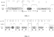
- FIG. 1 illustrates a schematic diagram of a waveform of an interrupt signal in a static mode of an exemplary LPC serial interrupt according to some embodiments of the present disclosure.
- an interrupt line is high.
- an external device or a peripheral needs to report an interrupt to a CPU, a start frame sent by the CPU, an interrupt bit sent by the external device, and an end frame sent by the CPU are sent to a SerIRQ interrupt signal all at one time.
- FIG. 2 illustrates a schematic diagram of a waveform of an interrupt signal in a continuous mode of an exemplary LPC serial interrupt according to some embodiments of the present disclosure.
- the CPU always sends the start frame and the end frame to the external device.
- the external device detects a position of a start frame, pulls down, at a position corresponding to an interrupt signal of the external device, a voltage level of the SerIRQ interrupt line of a corresponding moment, and sends the pulled-down voltage level signal to the CPU.
- the interrupt is reported to a general interrupt controller (GIC) circuit of the CPU. Then, the GIC circuit of the CPU processes the interrupt.
- GIC general interrupt controller
- the CPU is often fabricated with advanced technologies, the CPU requires a low operating voltage, such as 1.8 V, to reduce a power consumption of the CPU.
- the external device is often small in size because fewer chips and transistors as compared with the CPU are included, and does not require advanced technologies during fabrication, thereby resulting in a high operating voltage, such as 3.3 V.
- a signal at the high operating voltage can be inputted to a low-operating-voltage hardware and burn the low-operating-voltage hardware.
- a high-level signal outputted by the low-operating-voltage hardware that is inputted to a high-operating-voltage hardware may be incorrectly determined to be a low-level signal.
- the signals exchanged between the CPU and the external device need to be level-shifted, such that a receiving end receives a level-shifted signal.
- a specialized and complicated level-shifter circuit is used to shift a voltage level by comparing with a reference voltage, which requires hardware cost and time cost, and results in potential incorrect determination.
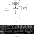
- FIG. 3 illustrates a schematic block diagram of an exemplary LPC serial interrupt system according to some embodiments of the present disclosure.
- the LPC serial interrupt system 300 includes a host 304 and an external device 305.
- the host 304 and the external device 305 send interrupt signals to each other.
- the LPC serial interrupt system 300 further includes: an interrupt direction signal generator 301 configured to determine a current interrupt direction signal SerIRQ_dir according to whether the host 304 currently sends a first interrupt signal to the external device 305, and a level-shifter 303 configured to shift a voltage level of a signal exchanged between the host 304 and the external device 305 according to the current interrupt direction signal SerIRQ_dir.
- the interrupt direction signal generator 301 is configured to perform the following steps to determine the current interrupt direction signal SerIRQ_dir according to whether the host 304 currently sends a first interrupt signal to the external device 305.
- the current interrupt direction signal SerIRQ_dir is determined to be from the host 304 to the external device 305, and a first signal indicating a direction from the host 304 to the external device 305 is generated.
- the first signal is a one-bit value 1, indicating that the host 304 outputs an interrupt signal.
- the current interrupt direction signal SerIRQ_dir is determined to be from the external device 305 to the host 304, and a second signal indicating a direction from the external device 305 to the host 304 is generated.
- the second signal is a one-bit value 0, indicating that the host 304 inputs an interrupt signal.
- the one-bit values 1 and 0 are for illustration purpose. In actual implementation, other values may be used.
- the host 304 is used as a reference for input and output because the host 304 is an actor of sending and receiving interrupt signals, and has the knowledge of whether the host 304 is sending or receiving interrupt signals.
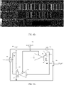
- FIG. 4A illustrate a timing diagram of a SerIRQ interrupt line and a SerIRQ_dir interrupt direction signal line in a continuous mode according to some embodiments of the present disclosure.
- FIG. 4B illustrate a timing diagram of a SerIRQ interrupt line and a SerIRQ_dir interrupt direction signal line in a static mode according to some embodiments of the present disclosure.
- the first interrupt signal includes one of an interrupt start signal and an interrupt end signal.
- the first interrupt signal includes both the interrupt start signal and the interrupt end signal.
- the interrupt start signal is, for example, the start frame shown in FIG. 1 or FIG. 2 , which often occupies 4 clock cycles to indicate a start of the interrupt signal.
- the interrupt end signal is, for example, the end frame shown in FIG. 1 or FIG. 2 , which often occupies 3 clock cycles to indicate an end of the interrupt signal.
- the voltage level of the SerIRQ interrupt line is pulled down.
- the first interrupt signal includes only the interrupt end signal because in the static mode, the start frame is not sent by the host, but is sent by the external device.
- the interrupt direction signal generator 301 determines that the current interrupt direction signal SerIRQ_dir is from the host 304 to the external device 305 when the host 304 currently sends the start frame or the end frame to the external device 305, and generates the first signal that indicates the direction from the host 304 to the external device 395.
- the interrupt direction signal generator 301 determines that the current interrupt direction signal SerIRQ_dir is from the external device 305 to the host 304, and generates the second signal that indicates the direction from the external device 305 to the host 304.
- the host 304 may actively report to the interrupt direction signal generator 301 whether the host currently sends out signals or not, such that the interrupt direction signal generator 301 sends out the interrupt direction signal SerIRQ_dir accordingly.
- the interrupt direction signal generator 301 is configured to: determine that the external device 305 currently sends the second interrupt signal to the host 304 when the host 304 currently does not send the first interrupt signal to the external device 305, determine that the current interrupt direction signal SerIRQ_dir is from the external device 305 to the host 304, and generate the second signal that indicates the direction from the external device 305 to the host 304.
- the second interrupt signal includes an external device interrupt identification signal.
- the external device interrupt identification signal is, for example, a portion that includes the interrupt bit except for the start frame and the end frame, as shown in FIG. 1 or FIG. 2 .
- the external device interrupt identification signal occupies n clock cycles, where n is a positive integer and is related to a quantity of external devices connected to the LPC bus.
- n is a positive integer and is related to a quantity of external devices connected to the LPC bus.
- one interrupt bit corresponds to one interrupt request from one external device.
- a position of the interrupt bit in the external device identification signal indicates which external device issued the interrupt request.
- x+1+y n.
- the second interrupt signal includes the external device interrupt identification signal and the interrupt start signal.
- the start frame is not sent by the host, but by the external device.
- the host is used as the reference for input and output, the host not sending a signal at a time can be interpreted as the external device potentially sending a signal at the time.
- the host 304 currently does not send the first interrupt signal to the external device 305, it is determined that the external device 305 currently sends the second interrupt signal to the host 304.
- the LPC serial interrupt system 300 further includes an interrupt direction signal register 302 configured to register the first signal or the second signal currently generated.
- the level-shifter 303 is configured to perform the following steps to convert the voltage level of the signals exchanged between the host 304 and the external device 305 according to the current interrupt direction signal SerlRQ_dir.
- a signal is retrieved from the interrupt direction signal register 302. If the signal retrieved from the interrupt direction signal register 302 is the first signal, the voltage level of the signal sent by the host 304 is changed from the voltage level operated by the host 304 to the voltage level operated by the external device 305. If the signal retrieved from the interrupt direction signal register 302 is the second signal, the voltage level of the signal sent by the externa; device 305 is changed from the voltage level operated by the external device 305 to the voltage level operated by the host 304.
- Table 1 below shows description of signals in the LPC serial interrupt system 300.
- Table 1 Signal name Host direction Description clk_33m I Controller internal clock signal rst_n I Reset signal SerIRQ_dir O Serial interrupt direction signal (binary 1 indicates output from the host, binary 0 indicates input into the host) SerIRQ I/O Serial interrupt signal Ldrq I DMA or bus host request signal, support single channel DMA request
- the level-shifter 303 is implemented in a complex programmable logic device (CPLD) or a field programmable gate array (FPGA) device.
- CPLD complex programmable logic device
- FPGA field programmable gate array
- FIG. 5A illustrates an internal circuit diagram of an exemplary level-shifter 303 (or first level-shifter) according to some embodiments of the present disclosure.
- the level-shifter 303 includes a host connection terminal A 501 connected to the host and an external device connection terminal B 502 connected to the external device.
- the level-shifter 303 further includes a host power supply VCCA 503 and an external device power supply VCCB 504.
- the host power supply VCCA is 1.6 V
- the external power supply VCCB is 3.3 V.
- the level-shifter 303 further includes a first inverter 505.
- a first input terminal of the first inverter 505 is connected to the host connection terminal A 501, and a second input terminal of the first inverter 505 receives the interrupt direction signal.
- the interrupt direction signal being 1 indicates that a signal is currently sent from the host to the external device.
- the interrupt direction signal has a high voltage level (e.g., 1.6 V) to enable the first inverter 505.
- the interrupt direction signal being 0 indicates that a signal is currently sent from the external device to the host.
- the interrupt direction signal has a low voltage level (e.g., 0 V) to disable the first inverter 505.
- the voltage level of the interrupt direction signal and a mechanism for enabling or disabling the first inverter 505 may be configured according to specific implementations, and may not be limited by the present disclosure.
- the level-shifter 303 further includes a first PMOS transistor P1 506.
- a drain electrode of the first PMOS transistor P1 506 is connected to the external device power supply 504.
- a source electrode of the first PMOS transistor P1 506 is connected to the external device connection terminal B 502 and a drain electrode of a first NMOS transistor N1 507.
- a gate electrode of the first PMOS transistor P1 506 is connected to an output terminal of the first inverter 505.
- the level-shifter 303 further includes the first NMOS transistor N1 507.
- a source electrode of the first NMOS transistor N1 507 is grounded.
- a gate electrode of the first NMOS transistor N1 507 is connected to the output terminal of the first inverter 505.
- the first inverter 505, the first PMOS transistor P1 506, the first NMOS transistor N1 507 are responsible for raising the voltage level of the signal from the host received by the host connection terminal A 501 to the voltage level suitable for the external device according to the interrupt direction signal.
- the interrupt direction signal when the interrupt direction signal is 1, it indicates that the signal is currently sent from the host to the external device. At this time, the interrupt direction signal has the high voltage level (e.g., 1.6 V) to enable the first inverter 505.
- the output terminal of the first inverter 505 outputs the low voltage level (e.g., 0 V).
- the first NMOS transistor N1 507 is turned off, and the first PMOS transistor P1 506 is turned on.
- the voltage level that the external device connection terminal B 502 outputs to the external device is changed to the external device power supply voltage VCCB, that is, 3.3 V.
- the interrupt direction signal when the interrupt direction signal is 0, it indicates that the signal is currently sent from the external device to the host. At this time, the interrupt direction signal has the low voltage level (e.g., 0 V) to disable the first inverter 505.
- the level-shifter 303 further includes a second inverter 508.
- a first input terminal of the second inverter 508 is connected to the external device connection terminal B 502.
- a second input terminal of the second inverter 508 receives the interrupt direction signal.
- the interrupt direction signal being 1 indicates that the signal is currently sent from the host to the external device. At this time, the interrupt direction signal has a high voltage level (e.g., 1.6 V) to disable the second inverter 508.
- the interrupt direction signal being 0 indicates that the signal is currently sent from the external device to the host. At this time, the interrupt direction signal has a low voltage level (e.g., 0 V) to enable the second inverter 508.
- the level-shifter 303 further includes a second PMOS transistor P2 509.
- a drain electrode of the second PMOS transistor P2 509 is connected to the host power supply 503.
- a source electrode of the second PMOS transistor P2 509 is connected to the host connection terminal A 501 and a drain electrode of a second NMOS transistor N2 510.
- a gate electrode of the second PMOS transistor P2 509 is connected to an output terminal of the second inverter 508.
- the level-shifter 303 further includes the second NMOS transistor N2 510.
- a source electrode of the second NMOS transistor N2 510 is grounded.
- a gate electrode of the second NMOS transistor N2 510 is connected to the output terminal of the second inverter 508.
- the second inverter 508, the second PMOS transistor P2 509, the second NMOS transistor N2 510 are responsible for lowering the voltage level of the signal from the external device received by the external device connection terminal B 502 to the voltage level suitable for the host according to the interrupt direction signal.
- the interrupt direction signal when the interrupt direction signal is 1, it indicates that the signal is currently sent from the host to the external device. At this time, the interrupt direction signal has the high voltage level (e.g., 1.6 V) to disable the second inverter 508. On the other hand, when the interrupt direction signal is 0, it indicates that the signal is currently sent from the external device to the host. At this time, the interrupt direction signal has the low voltage level (e.g., 0 V) to enable the second inverter 508. The output terminal of the second inverter 508 outputs the low voltage level (e.g., 0 V). Thus, the second NMOS transistor N2 510 is turned off, and the second PMOS transistor P2 509 is turned on. The voltage level that the host connection terminal A 501 outputs to the host is changed to the host power supply voltage VCCA, that is, 1.6 V.
- the host power supply voltage VCCA that is, 1.6 V.
- the LPC serial interrupt system 300 further includes a resistor R1.
- One end of the resistor R1 is connected to the host power supply VCCA 503. Another end of the resistor R1 is connected to the host connection terminal A 501, the first input terminal of the first inverter 505, the source electrode of the second PMOS transistor P2 509, and the drain electrode of the second NMOS transistor N2 510.
- the LPC serial interrupt system 300 further includes a resistor R2. One end of the resistor R2 is connected to the external device power supply VCCB 504. Another end of the resistor R2 is connected to the external device connection terminal B 502, the first input terminal of the second inverter 508, the source electrode of the first PMOS transistor P1 506, and the drain electrode of the first NMOS transistor N1 507.
- the level-shifter 303 shown in FIG. 5A may convert the voltage level between the host and the external device according to the interrupt direction signal.
- the LPC serial interrupt system 300 further includes: an interrupt mask register (not shown) configured to register an interrupt mask bit.
- an interrupt mask register (not shown) configured to register an interrupt mask bit.
- the interrupt mask bit is used to mask the second interrupt signal from the external device to the host. That is, even if the external device 305 sends an interrupt request to the host 304, the host 304 does not perform an interrupt operation.
- FIG. 5B illustrates an internal circuit diagram of another exemplary level-shifter 303' (or second level-shifter) according to some embodiments of the present disclosure.
- the level-shifter 303' includes a host connection terminal A 501' connected to the host and an external device connection terminal B 502' connected to the external device.
- the host connection terminal A and the external device connection terminal B also receive the interrupt direction signal from the interrupt direction signal generator 301 or the interrupt direction signal register 302 to learn the current signal direction.
- the level-shifter 303' further includes a host power supply VCCA 503' and an external device power supply VCCB 504'.
- the host power supply VCCA is 1.6 V
- the external power supply VCCB is 3.3 V.
- the level-shifter 303' further includes a first converter T1 505'.
- a first input terminal of the first converter T1 505' is connected to the external device connection terminal B 502', a second input terminal of the first converter T1 505" receives the interrupt direction signal from the interrupt direction signal generator, and an output terminal of the first converter T1 505' is connected to input terminals of a first one-shot accelerator OS1 506' and a second one-shot accelerator OS2 507'.
- the level-shifter 303' further includes a first PMOS transistor P1 508'.
- a drain electrode of the first PMOS transistor P1 508' is connected to the host power supply 503'.
- a source electrode of the first PMOS transistor P1 508' is connected to the host connection terminal A 501' and a drain electrode of a first NMOS transistor N1 509'.
- a gate electrode of the first PMOS transistor P1 508' is connected to an output terminal of the first one-shot accelerator OS1 506'.
- the level-shifter 303' further includes the first NMOS transistor N1 509'.
- a source electrode of the first NMOS transistor N1 509' is grounded.
- a gate electrode of the first NMOS transistor N1 509' is connected to an output terminal of the second one-shot accelerator OS2 507'.
- the level-shifter 303' further includes a second converter T2 510'.
- An input terminal of the second converter 510' is connected to the host connection terminal A 501'.
- An output terminal of the second converter 510' is connected to input terminals of a third one-shot accelerator OS3 511' and a fourth one-shot accelerator OS4 512'.
- the level-shifter 303' further includes a second PMOS transistor P2 513'.
- a drain electrode of the second PMOS transistor P2 513' is connected to the external device power supply 504'.
- a source electrode of the second PMOS transistor P2 513' is connected to the external connection terminal B 502' and a drain electrode of a second NMOS transistor N2 514'.
- a gate electrode of the second PMOS transistor P2 513' is connected to an output terminal of the third one-shot accelerator OS3 511'.
- the level-shifter 303' further includes the second NMOS transistor N2 514'.
- a source electrode of the second NMOS transistor N2 514' is grounded.
- a gate electrode of the second NMOS transistor N2 514' is connected to an output terminal of the fourth converter OS4 512'.
- the third one-shot accelerator OS3 511' turns on the second PMOS transistor P2 513' for a short period of time, thereby reducing a transition time from the low voltage level to the high voltage level.
- the fourth one-shot accelerator OS4 512' turns on the second NMOS transistor N2 514' for a short period of time, thereby speeding up a transition from the high voltage level to the low voltage level.
- the third one-shot accelerator OS3 511' and the fourth one-shot accelerator OS4 512' together form an edge rate accelerator at the external device connection terminal B 502'.
- the second PMOS transistor P2 513' and the second NMOS transistor N2 514' are used to quickly pull a terminal high or low when the corresponding transition is detected at the terminal.
- the first one-shot accelerator OS1 506' turns on the first PMOS transistor P1 508' for a short period of time, thereby reducing a transition time from the low voltage level to the high voltage level.
- the second one-shot accelerator OS2 507' turns on the first NMOS transistor N1 509' for a short period of time, thereby speeding up a transition from the high voltage level to the low voltage level.
- the first one-shot accelerator OS1 506', the second one-shot accelerator OS2 507', the first PMOS transistor P1 508', the first NMOS transistor N1 509' together form another edge rate accelerator at the host connection terminal A 501', which is used to force the voltage level of the host connection terminal A 501' to quickly rise or fall when a corresponding transition is detected at the external device connection terminal B 502'.
- the second PMOS transistor P2 513' and the second NMOS transistor N2 514' are used to quickly pull a terminal high or low when the corresponding transition is detected at the terminal.
- the third one-shot accelerator OS3 511', the fourth one-shot accelerator OS4 512', the second PMOS transistor P2 513', the second NMOS transistor N2 514' together form another edge rate accelerator at the external device connection terminal B 502', which is used to force the voltage level of the external device connection terminal B 502' to quickly rise or fall when a corresponding transition is detected at the host connection terminal A 501'.
- the level-shifter 303' further includes some resistors, such as a resistor RPUA, a resistor RPUB, a resistor R1, and a resistor R2.
- the level-shifter 303' further includes other transistors. The connection relationship thereof is clearly shown in FIG. 5B . Further description is omitted.
- the level-shifter 303' shown in FIG. 5B may convert the voltage level between the host and the external device according to the interrupt direction signal.
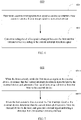
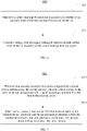
- FIG. 6 illustrates a flowchart of an exemplary LPC serial interrupt method 600 according to some embodiments of the present disclosure.
- the LPC serial interrupt method 600 includes: determining a current interrupt direction signal according to whether a host currently sends a first interrupt signal to an external device (step 601); and converting a voltage level of a signal exchanged between the host and the external device according to the current interrupt direction signal (step 602).
- FIG. 7 illustrates a flowchart of determining a current interrupt direction signal (step 601) in an exemplary LPC serial interrupt method 600 according to some embodiments of the present disclosure.
- step 601 includes: determining that the current interrupt direction signal is from the host to the external device and generating a first signal indicating a direction from the host to the external device when the host currently sends a first interrupt signal to the external device (step 6011); and determining that the current interrupt direction signal is from the external device to the host and generating a second signal indicting a direction from the external device to the host when the host currently does not send the first interrupt signal to the external device (step 6012).
- the first interrupt signal includes one of an interrupt start signal and an interrupt end signal.
- step 6012 further includes: determining that the external device currently sends a second interrupt signal to the host when the host currently does not send the first interrupt signal to the external device, determining that the current interrupt direction signal is from the external device to the host, and generating the second signal indicating the direction from the external device to the host.
- the second interrupt signal includes an external device interrupt identification signal.
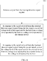
- FIG. 8 illustrates a flowchart of converting a voltage level (step 602) in an exemplary LPC serial interrupt method 600 according to some embodiments of the present disclosure.
- the method 600 further includes: using an interrupt direction signal register to register the currently generated first signal or second signal.
- Step 602 includes: retrieving a signal from the interrupt direction signal register (step 6021); changing the voltage level of the signal transmitted by the host from the voltage level suitable for the host to the voltage level suitable for the external device if the retrieved signal is the first signal (step 6022); and changing the voltage level of the signal transmitted by the external device from the voltage level suitable for the external device to the voltage level suitable for the host if the retrieved signal is the second signal (step 6023).
- the method 600 further includes: implementing, in a CPLD device or a FPGA device, the conversion of the voltage level of the signals exchanged between the host and the external device.
- a first level-shifter is used to convert the voltage of the signals exchanged between the host and the external device according to the current interrupt direction signal.
- the first level-shifter includes: a host connection terminal connected to the host and an external device connection terminal connected to the external device, a host power supply and an external device power supply, a first inverter, a first PMOS transistor, and a first NMOS transistor.
- a first input terminal of the first inverter is connected to the host connection terminal, and a second input terminal of the first inverter receives the interrupt direction signal.
- the interrupt direction signal indicates that a signal is currently sent from the host to the external device
- the interrupt direction signal enables the first inverter.
- the interrupt direction signal indicates that a signal is currently sent from the external device to the host, the interrupt direction signal disables the first inverter.
- a drain electrode of the first PMOS transistor is connected to the external device power supply.
- a source electrode of the first PMOS transistor is connected to the external device connection terminal and a drain electrode of the first NMOS transistor.
- a gate electrode of the first PMOS transistor is connected to an output terminal of the first inverter.
- a source electrode of the first NMOS transistor is grounded.
- a gate electrode of the first NMOS transistor is connected to the output terminal of the first inverter.
- converting the voltage level of the signals exchanged between the host and the external device according to the current interrupt direction signal further includes: when the interrupt direction signal indicates that the signal is currently sent from the host to the external device, enabling the first inverter to make the output terminal of the first inverter output a low voltage level, which turns off the first NMOS transistor and turns on the first PMOS transistor, thereby changing the voltage level that the external device connection terminal outputs to the external device to the external device power supply voltage; and when the interrupt direction signal indicates that the signal is currently sent from the external device to the host, disabling the first inverter.
- the first level-shifter further includes: a second inverter, a second PMOS transistor, and a second NMOS transistor.
- a first input terminal of the second inverter is connected to the external device connection terminal.
- a second input terminal of the second inverter receives the interrupt direction signal.
- the interrupt direction signal indicates that the signal is currently sent from the host to the external device
- the interrupt direction signal disables the second inverter.
- the interrupt direction signal indicates that the signal is currently sent from the external device to the host
- the interrupt direction signal enables the second inverter.
- a drain electrode of the second PMOS transistor is connected to the host power supply.
- a source electrode of the second PMOS transistor is connected to the host connection terminal and a drain electrode of the second NMOS transistor.
- a gate electrode of the second PMOS transistor is connected to an output terminal of the second inverter.
- a source electrode of the second NMOS transistor is grounded.
- a gate electrode of the second NMOS transistor is connected to the output terminal of the second inverter.
- converting the voltage level of the signals exchanged between the host and the external device according to the current interrupt direction signal further includes: when the interrupt direction signal indicates that the signal is currently sent from the host to the external device, disabling the second inverter, and when the interrupt direction signal indicates that the signal is currently sent from the external device to the host, enabling the second inverter to make the output terminal of the second inverter output a low voltage level, which turns off the second NMOS transistor and turns on the second PMOS transistor, thereby changing the voltage level that the host connection terminal outputs to the host to the host power supply voltage.
- a second level-shifter is used to convert the voltage level of the signals exchanged between the host and the external device according to the current interrupt direction signal.
- the second level-shifter includes: a host connection terminal connected to the host and an external device connection terminal connected to the external device, a host power supply and an external device power supply, a first converter, a first PMOS transistor, a first NMOS transistor, a second converter, a second PMOS transistor, and a second NMOS transistor.
- a first input terminal of the first converter is connected to the external device connection terminal
- a second input terminal of the first inverter receives the interrupt direction signal from the interrupt direction signal generator
- an output terminal of the first converter is connected to input terminals of a first one-shot accelerator and a second one-shot accelerator.
- a drain electrode of the first PMOS transistor is connected to the host power supply.
- a source electrode of the first PMOS transistor is connected to the host connection terminal and a drain electrode of the first NMOS transistor.
- a gate electrode of the first PMOS transistor is connected to an output terminal of the first one-shot accelerator.
- a source electrode of the first NMOS transistor is grounded.
- a gate electrode of the first NMOS transistor is connected to an output terminal of the second one-shot accelerator.
- a first input terminal of the second converter is connected to the host connection terminal.
- a second input terminal of the second converter receives the interrupt direction signal from the interrupt direction signal generator.
- An output terminal of the second converter is connected to input terminals of a third one-shot accelerator and a fourth one-shot accelerator.
- a drain electrode of the second PMOS transistor is connected to the external device power supply.
- a source electrode of the second PMOS transistor is connected to the external connection terminal and a drain electrode of the second NMOS transistor.
- a gate electrode of the second PMOS transistor is connected to an output terminal of the third one-shot accelerator.
- a source electrode of the second NMOS transistor is grounded.
- a gate electrode of the second NMOS transistor is connected to an output terminal of the fourth converter.
- the first one-shot accelerator when the interrupt direction signal indicates that the signal is transmitted from the external device to the host, during a rising edge, the first one-shot accelerator turns on the first PMOS transistor. During a falling edge, when the interrupt direction signal indicates that the signal is transmitted from the external device to the host, the second one-shot accelerator turns on the first NMOS transistor.
- the method 600 further includes: configuring to register an interrupt mask bit, and masking the external device from sending the second interrupt signal to the host when the interrupt mask bit is a pre-determined bit.
- FIG. 9 illustrates a schematic block diagram of an exemplary computer system for implementing various interrupt methods according to some embodiments of the present disclosure.
- the computer system includes a processor H1, a memory H2 coupled with the processor H1 and storing computer-executable instructions therein for performing various methods of the embodiments of the present disclosure when being executed by the processor H1.
- the processor H1 may include, but is not limited to, for example, one or more processors or microprocessors.
- the memory H2 may include, but is not limited to, for example, a random-access memory (RAM), a read-only memory (ROM), a flash memory, an erasable programmable read-only memory (EPROM), an electrically erasable programmable read-only memory (EEPROM), a register, a computer storage medium (e.g., a hard disk, a floppy disk, a solid-state hard drive, a removable disc, a compact disc read-only memory (CD-ROM), a digital versatile disc-read only memory (DVD-ROM), a Blue-ray disc, etc.), or a combination thereof.
- RAM random-access memory
- ROM read-only memory
- EPROM erasable programmable read-only memory
- EEPROM electrically erasable programmable read-only memory
- register e.g., a computer storage medium (e.g., a hard disk, a floppy disk, a solid-state hard drive, a removable disc, a compact disc
- the computer system may further include a data bus H3, an input/output bus H4, a display H5, and an input/output device H6 (e.g., a keyboard, a mouse, a speaker, etc.), or a combination thereof.
- a data bus H3 an input/output bus H4
- a display H5 e.g., a liquid crystal display
- an input/output device H6 e.g., a keyboard, a mouse, a speaker, etc.
- the processor H1 may use the input/output bus H4 to communicate with external devices (e.g., H5, H6) through a wired or wireless network (not shown).
- external devices e.g., H5, H6
- the memory H2 may further store at least one computer-executable instruction for executing each function and/or method step in the embodiments of the present disclosure when being executed by the processor H1.
- the at least one computer-executable instruction may also be compiled or formed into an LPC serial interrupt software product, where one or more computer-executable instructions are executed to implement each function and/or method step in the embodiments of the present disclosure when being executed by the processor H1.
- the means may include various hardware and/or software components and/or modules, including but not limited to hardware circuits, application specific integrated circuits (ASICs), or processors.
- ASICs application specific integrated circuits
- DSPs digital signal processors
- ASICs field programmable gate arrays
- FPGAs field programmable gate arrays
- PLDs programmable logic devices
- a general-purpose processor may be a microprocessor or may be any commercially available processors, controllers, microcontrollers, or state machines.
- the processor may also be a combination of computing devices, such as a combination of a DSP and a microprocessor, a plurality of microprocessors, a microprocessor cooperating with a DSP core, or another such combination.
- the steps of the method or algorithm described in the embodiments of the present disclosure can be directly embedded in hardware, a software module executed by a processor, or a combination of both.
- the software module may be stored in any form of physical storage medium, which includes, but is not limited to, a random-access memory (RAM), a read-only memory (ROM), a flash memory, an erasable programmable read-only memory (EPROM), an electrically erasable programmable read-only memory (EEPROM), a register, a computer storage medium (e.g., a hard disk, a floppy disk, a solid-state hard drive, a removable disc, a compact disc read-only memory (CD-ROM), a digital versatile disc-read only memory (DVD-ROM), a Blue-ray disc, etc.), or a combination thereof.
- RAM random-access memory
- ROM read-only memory
- EPROM erasable programmable read-only memory
- EEPROM electrically erasable programmable read-only memory
- the storage medium may be coupled with the processor such that the processor can retrieve information from and write information to the storage medium.
- the storage medium may be integral to the processor.
- the software module may be a single instruction or a plurality of instructions, and can be distributed in different code segments, between different programs, and across multiple storage media.
- the disclosed methods include actions for implementing the described methods.
- the methods and/or actions can be interchanged with each other without departing from the scope of claims.
- the order and/or use of specific actions can be modified without departing from the scope of the claims.
- the above-described functions can be implemented by hardware, software, firmware or a combination thereof. If implemented in software, the functions can be stored as instructions on a physical computer-readable medium.
- the storage medium may be any available physical medium that can be accessed by a computer.
- the computer-readable medium may include a RAM, a ROM, an EEPROM, a CD-ROM or other optical storage, a magnetic disc storage or other magnetic storage device or any other physical medium that can carry or store instructions or data structures in the form of a desired program code and can be accessed by the computer.
- the disk and the disc used herein may include a compact disc (CD), a laser disc, an optical disc, a DVD, a floppy disk, and a Blue-ray disc, where the disk often reproduces data magnetically while the disc often use a laser to reproduce data optically.
- CD compact disc
- laser disc an optical disc
- DVD a DVD
- floppy disk a floppy disk
- Blue-ray disc where the disk often reproduces data magnetically while the disc often use a laser to reproduce data optically.
- the computer program product may perform the described operations.
- the computer program product may be computer-readable physical medium having instructions physically stored (and/or encoded) thereon, and the instructions can be executed by a processor to perform the operations described herein.
- the computer program product may include packaging materials.
- Software or instructions may also be transmitted through a transmission medium.
- a transmission medium such as a coaxial cable, a fiber optic cable, a twisted pair, a digital subscriber line (DSL), or a wireless technology such as infrared, radio, or microwave, may be used to transmit software from a website, a server, or another remote source.
- DSL digital subscriber line
- a wireless technology such as infrared, radio, or microwave
- modules and/or other appropriate means used to perform the methods and technologies described herein may be downloaded by a user terminal and/or a base station and/or obtained by other means.
- the device may be coupled with the server to facilitate the transmission of functions for performing the methods described herein.
- various methods described herein may be provided via storage components (e.g., a RAM, a ROM, a physical storage medium such as a CD or a floppy disk), such that the user terminal and/or the base station may obtain various methods by being coupled with the device or providing a storage component to the device.
- any other suitable techniques for providing the methods and functions described herein to the device may be utilized.
Landscapes
- Engineering & Computer Science (AREA)
- Theoretical Computer Science (AREA)
- Physics & Mathematics (AREA)
- General Engineering & Computer Science (AREA)
- General Physics & Mathematics (AREA)
- Computer Hardware Design (AREA)
- Mathematical Physics (AREA)
- Computing Systems (AREA)
- Logic Circuits (AREA)
- Bus Control (AREA)
Applications Claiming Priority (1)
| Application Number | Priority Date | Filing Date | Title |
|---|---|---|---|
| CN202110053101.5A CN112711558B (zh) | 2021-01-15 | 2021-01-15 | Lpc总线的串行中断系统、方法、介质 |
Publications (3)
| Publication Number | Publication Date |
|---|---|
| EP4040301A2 true EP4040301A2 (de) | 2022-08-10 |
| EP4040301A3 EP4040301A3 (de) | 2022-10-12 |
| EP4040301B1 EP4040301B1 (de) | 2025-06-04 |
Family
ID=75549111
Family Applications (1)
| Application Number | Title | Priority Date | Filing Date |
|---|---|---|---|
| EP22151504.2A Active EP4040301B1 (de) | 2021-01-15 | 2022-01-14 | Verfahren und system zur seriellen unterbrechung einer sammelleitung mit niedriger pin-zahl (lpc) |
Country Status (3)
| Country | Link |
|---|---|
| US (1) | US12026111B2 (de) |
| EP (1) | EP4040301B1 (de) |
| CN (1) | CN112711558B (de) |
Family Cites Families (21)
| Publication number | Priority date | Publication date | Assignee | Title |
|---|---|---|---|---|
| US5047663A (en) * | 1989-07-28 | 1991-09-10 | Dallas Semiconductor Corporation | Low-power comparator which tolerates high-slew-rate incoming signals and deriving power from the incoming signals |
| US5619066A (en) * | 1990-05-15 | 1997-04-08 | Dallas Semiconductor Corporation | Memory for an electronic token |
| US5754436A (en) * | 1994-12-22 | 1998-05-19 | Texas Instruments Incorporated | Adaptive power management processes, circuits and systems |
| JPH0935479A (ja) * | 1995-07-14 | 1997-02-07 | Oki Electric Ind Co Ltd | 電流アンプ及びデータバス回路 |
| WO2002086747A1 (en) * | 2001-04-24 | 2002-10-31 | Broadcom Corporation | Integrated gigabit ethernet pci-x controller |
| CN1820295A (zh) * | 2003-05-07 | 2006-08-16 | 东芝松下显示技术有限公司 | El显示装置及其驱动方法 |
| US7752365B2 (en) * | 2008-04-01 | 2010-07-06 | Kyocera Corporation | Bi-directional single conductor interrupt line for communication bus |
| US9288555B2 (en) * | 2011-11-01 | 2016-03-15 | Plexxi Inc. | Data center network architecture |
| US9337931B2 (en) * | 2011-11-01 | 2016-05-10 | Plexxi Inc. | Control and provisioning in a data center network with at least one central controller |
| CN103914424B (zh) * | 2014-04-14 | 2016-08-03 | 中国人民解放军国防科学技术大学 | 基于gpio接口的lpc外设扩展方法及装置 |
| US9407266B2 (en) * | 2014-08-22 | 2016-08-02 | Xilinx, Inc. | Programmable single-supply level-shifter circuit |
| CN105512070B (zh) * | 2015-12-02 | 2018-07-06 | 中国电子科技集团公司第四十一研究所 | 一种基于串行总线的控制系统 |
| US10725844B2 (en) * | 2016-11-03 | 2020-07-28 | Foxconn eMS, Inc. | Automated boot failure prevention and recovery circuit and related method |
| US20190265976A1 (en) * | 2018-02-23 | 2019-08-29 | Yuly Goryavskiy | Additional Channel for Exchanging Useful Information |
| US11792307B2 (en) * | 2018-03-28 | 2023-10-17 | Apple Inc. | Methods and apparatus for single entity buffer pool management |
| CN108763140B (zh) * | 2018-04-23 | 2021-02-12 | 深圳市文鼎创数据科技有限公司 | 一种双向通信的方法、系统及终端设备 |
| CN209433401U (zh) * | 2019-04-22 | 2019-09-24 | 山东超越数控电子股份有限公司 | 一种国产平台实现系统中断的结构 |
| US10965221B1 (en) * | 2020-09-01 | 2021-03-30 | King Abdulaziz University | Switched capacitor based boost inverter topology with a higher number of levels and higher voltage gain |
| US11887691B2 (en) * | 2020-10-01 | 2024-01-30 | University Of Maryland, College Park | Temporal memory systems and methods |
| US11513991B2 (en) * | 2020-10-01 | 2022-11-29 | Qualcomm Incorporated | Batch operation across an interface |
| KR102948817B1 (ko) * | 2021-12-31 | 2026-04-07 | 주식회사 엘엑스세미콘 | 전원관리회로 및 이를 포함하는 표시장치 |
-
2021
- 2021-01-15 CN CN202110053101.5A patent/CN112711558B/zh active Active
-
2022
- 2022-01-13 US US17/575,340 patent/US12026111B2/en active Active
- 2022-01-14 EP EP22151504.2A patent/EP4040301B1/de active Active
Also Published As
| Publication number | Publication date |
|---|---|
| US12026111B2 (en) | 2024-07-02 |
| CN112711558B (zh) | 2023-07-21 |
| EP4040301B1 (de) | 2025-06-04 |
| CN112711558A (zh) | 2021-04-27 |
| EP4040301A3 (de) | 2022-10-12 |
| US20220229793A1 (en) | 2022-07-21 |
Similar Documents
| Publication | Publication Date | Title |
|---|---|---|
| CN107077443B (zh) | 用于动态枚举总线的预定义静态枚举 | |
| CN106663078B (zh) | 延迟电路以及相关的系统和方法 | |
| US8850175B2 (en) | Computer apparatus and resetting method for real time clock thereof | |
| EP3283971B1 (de) | Steuerkreise zur erzeugung von ausgangsfreigabesignalen sowie entsprechende systeme und verfahren | |
| CN103116402A (zh) | 具有语音控制功能的计算机系统以及语音控制方法 | |
| CN112069040B (zh) | 一种硬盘点灯方法、装置及相关组件 | |
| US9019752B1 (en) | Static random access memory (SRAM) global bitline circuits for reducing power glitches during memory read accesses, and related methods and systems | |
| CN108446139B (zh) | 一种fpga芯片的唤醒方法及装置 | |
| CN208848137U (zh) | 具有充电功能的主机板 | |
| US10613832B2 (en) | Random number generating system and random number generating method thereof | |
| EP4040301A2 (de) | Verfahren und system zur seriellen unterbrechung einer sammelleitung mit niedriger pin-zahl (lpc) | |
| US9608637B2 (en) | Dynamic voltage level shifters employing pulse generation circuits, and related systems and methods | |
| CN112583063B (zh) | 控制器、充电线缆、识别充电线缆类型的系统及方法 | |
| US11927980B2 (en) | Electronic device and powering method thereof | |
| CN115543056B (zh) | 一种供电装置、方法、设备、系统及介质 | |
| Zhang et al. | A QSPI Interface Supporting ‘Bits-Decoding’for High-Speed Access to Flash | |
| US12211578B2 (en) | DDR PHY power collapse circuit for multimode double data rate synchronous dynamic random access memory | |
| CN117148954A (zh) | 微控制器及电子设备 | |
| TWI662764B (zh) | 具有智能充電功能的主機板 | |
| CN114462337A (zh) | 时序逻辑的综合方法及装置、设备、存储介质 | |
| CN113676164B (zh) | 脉冲调制控制系统、装置及方法 | |
| US20100023662A1 (en) | Bus mastering method | |
| JP2009239344A (ja) | 記述処理装置、記述処理方法およびプログラム | |
| CN110008155B (zh) | 电子装置及其操作方法 | |
| CN106033231A (zh) | 一种信息处理方法、时钟分频装置及信息处理系统 |
Legal Events
| Date | Code | Title | Description |
|---|---|---|---|
| PUAI | Public reference made under article 153(3) epc to a published international application that has entered the european phase |
Free format text: ORIGINAL CODE: 0009012 |
|
| STAA | Information on the status of an ep patent application or granted ep patent |
Free format text: STATUS: THE APPLICATION HAS BEEN PUBLISHED |
|
| AK | Designated contracting states |
Kind code of ref document: A2 Designated state(s): AL AT BE BG CH CY CZ DE DK EE ES FI FR GB GR HR HU IE IS IT LI LT LU LV MC MK MT NL NO PL PT RO RS SE SI SK SM TR |
|
| PUAL | Search report despatched |
Free format text: ORIGINAL CODE: 0009013 |
|
| AK | Designated contracting states |
Kind code of ref document: A3 Designated state(s): AL AT BE BG CH CY CZ DE DK EE ES FI FR GB GR HR HU IE IS IT LI LT LU LV MC MK MT NL NO PL PT RO RS SE SI SK SM TR |
|
| RIC1 | Information provided on ipc code assigned before grant |
Ipc: H04L 5/14 20060101ALI20220907BHEP Ipc: H03K 17/10 20060101ALI20220907BHEP Ipc: H03K 19/0185 20060101ALI20220907BHEP Ipc: H03K 19/0175 20060101ALI20220907BHEP Ipc: G06F 13/42 20060101ALI20220907BHEP Ipc: G06F 13/40 20060101ALI20220907BHEP Ipc: G06F 13/38 20060101ALI20220907BHEP Ipc: G06F 13/24 20060101AFI20220907BHEP |
|
| STAA | Information on the status of an ep patent application or granted ep patent |
Free format text: STATUS: REQUEST FOR EXAMINATION WAS MADE |
|
| 17P | Request for examination filed |
Effective date: 20230302 |
|
| RBV | Designated contracting states (corrected) |
Designated state(s): AL AT BE BG CH CY CZ DE DK EE ES FI FR GB GR HR HU IE IS IT LI LT LU LV MC MK MT NL NO PL PT RO RS SE SI SK SM TR |
|
| STAA | Information on the status of an ep patent application or granted ep patent |
Free format text: STATUS: EXAMINATION IS IN PROGRESS |
|
| 17Q | First examination report despatched |
Effective date: 20230510 |
|
| GRAP | Despatch of communication of intention to grant a patent |
Free format text: ORIGINAL CODE: EPIDOSNIGR1 |
|
| STAA | Information on the status of an ep patent application or granted ep patent |
Free format text: STATUS: GRANT OF PATENT IS INTENDED |
|
| RIC1 | Information provided on ipc code assigned before grant |
Ipc: H03K 19/17784 20200101ALI20241216BHEP Ipc: H03K 19/017 20060101ALI20241216BHEP Ipc: G06F 13/28 20060101ALI20241216BHEP Ipc: H03K 17/10 20060101ALI20241216BHEP Ipc: H04L 5/14 20060101ALI20241216BHEP Ipc: H03K 19/0185 20060101ALI20241216BHEP Ipc: H03K 19/0175 20060101ALI20241216BHEP Ipc: G06F 13/42 20060101ALI20241216BHEP Ipc: G06F 13/40 20060101ALI20241216BHEP Ipc: G06F 13/38 20060101ALI20241216BHEP Ipc: G06F 13/24 20060101AFI20241216BHEP |
|
| INTG | Intention to grant announced |
Effective date: 20250103 |
|
| GRAS | Grant fee paid |
Free format text: ORIGINAL CODE: EPIDOSNIGR3 |
|
| GRAA | (expected) grant |
Free format text: ORIGINAL CODE: 0009210 |
|
| STAA | Information on the status of an ep patent application or granted ep patent |
Free format text: STATUS: THE PATENT HAS BEEN GRANTED |
|
| AK | Designated contracting states |
Kind code of ref document: B1 Designated state(s): AL AT BE BG CH CY CZ DE DK EE ES FI FR GB GR HR HU IE IS IT LI LT LU LV MC MK MT NL NO PL PT RO RS SE SI SK SM TR |
|
| REG | Reference to a national code |
Ref country code: GB Ref legal event code: FG4D |
|
| REG | Reference to a national code |
Ref country code: CH Ref legal event code: EP |
|
| REG | Reference to a national code |
Ref country code: DE Ref legal event code: R096 Ref document number: 602022015315 Country of ref document: DE |
|
| REG | Reference to a national code |
Ref country code: IE Ref legal event code: FG4D |
|
| REG | Reference to a national code |
Ref country code: NL Ref legal event code: MP Effective date: 20250604 |
|
| PG25 | Lapsed in a contracting state [announced via postgrant information from national office to epo] |
Ref country code: FI Free format text: LAPSE BECAUSE OF FAILURE TO SUBMIT A TRANSLATION OF THE DESCRIPTION OR TO PAY THE FEE WITHIN THE PRESCRIBED TIME-LIMIT Effective date: 20250604 Ref country code: ES Free format text: LAPSE BECAUSE OF FAILURE TO SUBMIT A TRANSLATION OF THE DESCRIPTION OR TO PAY THE FEE WITHIN THE PRESCRIBED TIME-LIMIT Effective date: 20250604 |
|
| REG | Reference to a national code |
Ref country code: LT Ref legal event code: MG9D |
|
| PG25 | Lapsed in a contracting state [announced via postgrant information from national office to epo] |
Ref country code: GR Free format text: LAPSE BECAUSE OF FAILURE TO SUBMIT A TRANSLATION OF THE DESCRIPTION OR TO PAY THE FEE WITHIN THE PRESCRIBED TIME-LIMIT Effective date: 20250905 Ref country code: NO Free format text: LAPSE BECAUSE OF FAILURE TO SUBMIT A TRANSLATION OF THE DESCRIPTION OR TO PAY THE FEE WITHIN THE PRESCRIBED TIME-LIMIT Effective date: 20250904 |
|
| PG25 | Lapsed in a contracting state [announced via postgrant information from national office to epo] |
Ref country code: PL Free format text: LAPSE BECAUSE OF FAILURE TO SUBMIT A TRANSLATION OF THE DESCRIPTION OR TO PAY THE FEE WITHIN THE PRESCRIBED TIME-LIMIT Effective date: 20250604 |
|
| PG25 | Lapsed in a contracting state [announced via postgrant information from national office to epo] |
Ref country code: BG Free format text: LAPSE BECAUSE OF FAILURE TO SUBMIT A TRANSLATION OF THE DESCRIPTION OR TO PAY THE FEE WITHIN THE PRESCRIBED TIME-LIMIT Effective date: 20250604 |
|
| PG25 | Lapsed in a contracting state [announced via postgrant information from national office to epo] |
Ref country code: HR Free format text: LAPSE BECAUSE OF FAILURE TO SUBMIT A TRANSLATION OF THE DESCRIPTION OR TO PAY THE FEE WITHIN THE PRESCRIBED TIME-LIMIT Effective date: 20250604 |
|
| PG25 | Lapsed in a contracting state [announced via postgrant information from national office to epo] |
Ref country code: RS Free format text: LAPSE BECAUSE OF FAILURE TO SUBMIT A TRANSLATION OF THE DESCRIPTION OR TO PAY THE FEE WITHIN THE PRESCRIBED TIME-LIMIT Effective date: 20250904 |
|
| PG25 | Lapsed in a contracting state [announced via postgrant information from national office to epo] |
Ref country code: LV Free format text: LAPSE BECAUSE OF FAILURE TO SUBMIT A TRANSLATION OF THE DESCRIPTION OR TO PAY THE FEE WITHIN THE PRESCRIBED TIME-LIMIT Effective date: 20250604 |
|
| PG25 | Lapsed in a contracting state [announced via postgrant information from national office to epo] |
Ref country code: NL Free format text: LAPSE BECAUSE OF FAILURE TO SUBMIT A TRANSLATION OF THE DESCRIPTION OR TO PAY THE FEE WITHIN THE PRESCRIBED TIME-LIMIT Effective date: 20250604 |
|
| PG25 | Lapsed in a contracting state [announced via postgrant information from national office to epo] |
Ref country code: PT Free format text: LAPSE BECAUSE OF FAILURE TO SUBMIT A TRANSLATION OF THE DESCRIPTION OR TO PAY THE FEE WITHIN THE PRESCRIBED TIME-LIMIT Effective date: 20251006 |
|
| REG | Reference to a national code |
Ref country code: AT Ref legal event code: MK05 Ref document number: 1801011 Country of ref document: AT Kind code of ref document: T Effective date: 20250604 |
|
| PG25 | Lapsed in a contracting state [announced via postgrant information from national office to epo] |
Ref country code: IS Free format text: LAPSE BECAUSE OF FAILURE TO SUBMIT A TRANSLATION OF THE DESCRIPTION OR TO PAY THE FEE WITHIN THE PRESCRIBED TIME-LIMIT Effective date: 20251004 |
|
| PG25 | Lapsed in a contracting state [announced via postgrant information from national office to epo] |
Ref country code: SM Free format text: LAPSE BECAUSE OF FAILURE TO SUBMIT A TRANSLATION OF THE DESCRIPTION OR TO PAY THE FEE WITHIN THE PRESCRIBED TIME-LIMIT Effective date: 20250604 Ref country code: AT Free format text: LAPSE BECAUSE OF FAILURE TO SUBMIT A TRANSLATION OF THE DESCRIPTION OR TO PAY THE FEE WITHIN THE PRESCRIBED TIME-LIMIT Effective date: 20250604 |
|
| PG25 | Lapsed in a contracting state [announced via postgrant information from national office to epo] |
Ref country code: CZ Free format text: LAPSE BECAUSE OF FAILURE TO SUBMIT A TRANSLATION OF THE DESCRIPTION OR TO PAY THE FEE WITHIN THE PRESCRIBED TIME-LIMIT Effective date: 20250604 |
|
| PG25 | Lapsed in a contracting state [announced via postgrant information from national office to epo] |
Ref country code: EE Free format text: LAPSE BECAUSE OF FAILURE TO SUBMIT A TRANSLATION OF THE DESCRIPTION OR TO PAY THE FEE WITHIN THE PRESCRIBED TIME-LIMIT Effective date: 20250604 |
|
| PG25 | Lapsed in a contracting state [announced via postgrant information from national office to epo] |
Ref country code: SK Free format text: LAPSE BECAUSE OF FAILURE TO SUBMIT A TRANSLATION OF THE DESCRIPTION OR TO PAY THE FEE WITHIN THE PRESCRIBED TIME-LIMIT Effective date: 20250604 |
|
| PG25 | Lapsed in a contracting state [announced via postgrant information from national office to epo] |
Ref country code: IT Free format text: LAPSE BECAUSE OF FAILURE TO SUBMIT A TRANSLATION OF THE DESCRIPTION OR TO PAY THE FEE WITHIN THE PRESCRIBED TIME-LIMIT Effective date: 20250604 |
|
| REG | Reference to a national code |
Ref country code: DE Ref legal event code: R097 Ref document number: 602022015315 Country of ref document: DE |
|
| PLBE | No opposition filed within time limit |
Free format text: ORIGINAL CODE: 0009261 |
|
| STAA | Information on the status of an ep patent application or granted ep patent |
Free format text: STATUS: NO OPPOSITION FILED WITHIN TIME LIMIT |
|
| PG25 | Lapsed in a contracting state [announced via postgrant information from national office to epo] |
Ref country code: DK Free format text: LAPSE BECAUSE OF FAILURE TO SUBMIT A TRANSLATION OF THE DESCRIPTION OR TO PAY THE FEE WITHIN THE PRESCRIBED TIME-LIMIT Effective date: 20250604 |
|
| PGFP | Annual fee paid to national office [announced via postgrant information from national office to epo] |
Ref country code: DE Payment date: 20260130 Year of fee payment: 5 |
|
| REG | Reference to a national code |
Ref country code: CH Ref legal event code: L10 Free format text: ST27 STATUS EVENT CODE: U-0-0-L10-L00 (AS PROVIDED BY THE NATIONAL OFFICE) Effective date: 20260416 |