EP4033744B1 - Dispositif et procédé d'amélioration de la reproductibilité des enregistrements - Google Patents
Dispositif et procédé d'amélioration de la reproductibilité des enregistrements Download PDFInfo
- Publication number
- EP4033744B1 EP4033744B1 EP21152490.5A EP21152490A EP4033744B1 EP 4033744 B1 EP4033744 B1 EP 4033744B1 EP 21152490 A EP21152490 A EP 21152490A EP 4033744 B1 EP4033744 B1 EP 4033744B1
- Authority
- EP
- European Patent Office
- Prior art keywords
- pixel
- line
- pixels
- light
- pixel array
- Prior art date
- Legal status (The legal status is an assumption and is not a legal conclusion. Google has not performed a legal analysis and makes no representation as to the accuracy of the status listed.)
- Active
Links
Images


Classifications
-
- H—ELECTRICITY
- H04—ELECTRIC COMMUNICATION TECHNIQUE
- H04N—PICTORIAL COMMUNICATION, e.g. TELEVISION
- H04N1/00—Scanning, transmission or reproduction of documents or the like, e.g. facsimile transmission; Details thereof
- H04N1/024—Details of scanning heads ; Means for illuminating the original
- H04N1/028—Details of scanning heads ; Means for illuminating the original for picture information pick-up
- H04N1/03—Details of scanning heads ; Means for illuminating the original for picture information pick-up with photodetectors arranged in a substantially linear array
- H04N1/031—Details of scanning heads ; Means for illuminating the original for picture information pick-up with photodetectors arranged in a substantially linear array the photodetectors having a one-to-one and optically positive correspondence with the scanned picture elements, e.g. linear contact sensors
-
- H—ELECTRICITY
- H04—ELECTRIC COMMUNICATION TECHNIQUE
- H04N—PICTORIAL COMMUNICATION, e.g. TELEVISION
- H04N1/00—Scanning, transmission or reproduction of documents or the like, e.g. facsimile transmission; Details thereof
- H04N1/04—Scanning arrangements, i.e. arrangements for the displacement of active reading or reproducing elements relative to the original or reproducing medium, or vice versa
- H04N1/19—Scanning arrangements, i.e. arrangements for the displacement of active reading or reproducing elements relative to the original or reproducing medium, or vice versa using multi-element arrays
- H04N1/191—Scanning arrangements, i.e. arrangements for the displacement of active reading or reproducing elements relative to the original or reproducing medium, or vice versa using multi-element arrays the array comprising a one-dimensional array, or a combination of one-dimensional arrays, or a substantially one-dimensional array, e.g. an array of staggered elements
- H04N1/1911—Simultaneously or substantially simultaneously scanning picture elements on more than one main scanning line, e.g. scanning in swaths
- H04N1/1912—Scanning main scanning lines which are spaced apart from one another in the sub-scanning direction
-
- H—ELECTRICITY
- H04—ELECTRIC COMMUNICATION TECHNIQUE
- H04N—PICTORIAL COMMUNICATION, e.g. TELEVISION
- H04N1/00—Scanning, transmission or reproduction of documents or the like, e.g. facsimile transmission; Details thereof
- H04N1/024—Details of scanning heads ; Means for illuminating the original
- H04N1/028—Details of scanning heads ; Means for illuminating the original for picture information pick-up
- H04N1/02815—Means for illuminating the original, not specific to a particular type of pick-up head
- H04N1/02895—Additional elements in the illumination means or cooperating with the illumination means, e.g. filters
-
- H—ELECTRICITY
- H04—ELECTRIC COMMUNICATION TECHNIQUE
- H04N—PICTORIAL COMMUNICATION, e.g. TELEVISION
- H04N1/00—Scanning, transmission or reproduction of documents or the like, e.g. facsimile transmission; Details thereof
- H04N1/04—Scanning arrangements, i.e. arrangements for the displacement of active reading or reproducing elements relative to the original or reproducing medium, or vice versa
- H04N1/0402—Scanning different formats; Scanning with different densities of dots per unit length, e.g. different numbers of dots per inch (dpi); Conversion of scanning standards
- H04N1/0408—Different densities of dots per unit length
- H04N1/0414—Different densities of dots per unit length in the sub scanning direction
-
- H—ELECTRICITY
- H04—ELECTRIC COMMUNICATION TECHNIQUE
- H04N—PICTORIAL COMMUNICATION, e.g. TELEVISION
- H04N2201/00—Indexing scheme relating to scanning, transmission or reproduction of documents or the like, and to details thereof
- H04N2201/0077—Types of the still picture apparatus
- H04N2201/0081—Image reader
Definitions
- the invention relates to a device and a method for improving the reproducibility of recordings, by means of which a reduction or removal of the moiré effect is made possible.
- the moiré effect is an optical effect in which the superimposition of regular grids or patterns creates a periodic grid or pattern that has special structures that are not present in any of the individual grids and that vary when the way they are superimposed is changed. This effect can occur when at least two grids that can be relatively finely designed overlap. It is a type of optical interference that can create certain grids that usually appear quite coarse in their design.
- the moiré effect can be compared to an optical illusion.
- the moiré effect can occur in image processing whenever two or more grids overlap, for example when at least one banknote is captured using at least one image sensor, when motifs with a regular structure are recorded. An image sensor can also record individual pixels using a specific grid. When processing banknotes, three regular grids can occur.
- a banknote can have locally parallel lines.
- regular scanning can take place in the transport direction.
- regular scanning in the line direction can also take place.
- the locally parallel lines and the regular scanning in the transport direction can cause a moiré effect if, for example, a scan has gaps.
- the locally parallel lines and the regular scanning in the line direction mean that, for example, no moiré effect is generated if a scan in the line direction has no gaps or only small, negligible gaps.
- FIG. 1A, FIG. 1B and FIG. 1C Each of these images shows a (always the same) 50-euro banknote 100, which was recorded or captured in three different positions using an image sensor, for example a conventional contact image sensor.
- a 50-euro banknote 100 has a bridge arch below it, see the arrows 102a and 102b in the FIG. 1A, FIG. 1B, FIG. 1C , a plurality of line structures running in one direction.
- the moiré effect can arise in very different patterns as an interaction between the structures on the motif and the scanning structure, which at least one image sensor, for example a conventional contact image sensor of a scanner, has (see, for example, the arrows 102a and 102b in the FIG. 1A, FIG. 1B and FIG. 1C ). Due to the different angles or small shifts in the scanning at which the 50-euro banknote is recorded by the image sensor, different unwanted moiré effect patterns are formed. If the 50-euro banknote is recorded with a fine pattern, the grid of the image sensor and the grid created by the fine pattern of the banknote affect each other.
- FIG. 1A, FIG. 1B and FIG. 1C occur mainly due to the different slant of banknotes that often occurs in practice and/or the different phase position of the scanning grid to the periodic lines and a pixel area that is too small compared to the scanning step. In principle, pixels that are too large compared to the scanning step can also lead to moiré effects.
- RGB color values may not be able to be measured at the same position due to time-multiplexing at, for example, 100 dots per inch (dpi), which can lead to reduced accuracy of color tone measurements, for example to spotting in the recorded image.
- a Nyquist criterion may also not be met in a transport direction of a banknote, for example at a resolution of 50 dpi, which is recorded at different slant angles, which can lead to low accuracy in the printing area. Consequently, reproducibility of image recordings, for example of banknotes, cannot be guaranteed.
- WO 99/35618 A1 discloses a currency validator for evaluating banknotes comprising a housing combining an inlet for receiving banknotes, a scanning path along which a received banknote is moved for evaluation, and a drive arrangement associated with the scanning path. Scanners of different types are provided in removable modules, whereby the scanners and their position can be varied by replacing the module with another module.
- the US 2005/045809 A1 discloses a photosensor assembly having multiple rows of photosensors sharing a charge transfer register. Charges from one row of photosensors are transferred to the charge transfer register through another row of photosensors, and charges from both rows of photosensors are optionally added in the charge transfer register.
- the photosensors in the two rows may have different light collection areas
- the device and the method are intended to enable a moiré-free image of, for example, banknotes.
- the device and the method described here are intended to enable a moiré-free image of banknotes by adapting a scan in the transport direction.
- the device and the method described here are intended to improve image reproducibility.
- the device and the method described here are intended to make the images of a banknote independent of different diagonal lines and/or different scanning locations.
- a plurality of recording types can be set using the device and the method described here.
- a larger scanning area can be achieved using the device and the method described here.
- the reproducibility of the images of a banknote can be improved using the device and the method described here.
- a signal-to-noise ratio can be improved by means of the device and the method described herein.
- the light source may be on the same (incident light measurement) and/or the opposite (transmitted light measurement) side as the image plane with respect to the object plane.
- the transmitted light measurement may be a bright field and/or dark field configuration.
- the light-sensitive line pixel array may comprise at least one photodiode line pixel array.
- a number of row pixel arrays may be less than a number of pixels in each row pixel array.
- a contact image sensor may have a line pixel array with, for example, about 800 pixels in a line and may have, for example, two lines.
- the object may be a security, such as a banknote or a check.
- the device may be a securities reader, for example a banknote and/or check reader.
- the drive device can have a plurality of rollers and at least one drive motor.
- the drive motor can be set up to drive at least one roller, for example a drive roller, such that at least one object can be driven along the transport direction on the guide device in the object plane and transported by means of guide rollers.
- the at least one light source can be a light-emitting diode (LED) light source, for example a monochrome LED or an RGB LED for color illumination of an object in the object plane.
- the light source can have a plurality of light sources in a direction perpendicular or transverse to a transport direction.
- the at least one light source can have at least one diode rod with light output.
- the at least one light source can be configured as a light guide with light output, which can be fed laterally with LEDs of different wavelengths.
- a rod lens can be, for example, a cylindrical lens.
- At least one rod lens can be designed as a gradient index lens. In various embodiments, at least one rod lens can be designed as a gradient index rod lens.
- the at least one rod lens can have a cylindrical shape in which the two end surfaces are polished and the lateral surface can be optically irrelevant.
- a rod lens can be available with different optical materials, for example with glasses such as quartz glass, but also with crystalline materials or plastic.
- the rod lenses can have a diameter in a value range of about 0.1 millimeters to 2 millimeters and, for example, a length range of 2 millimeters to 50 millimeters.
- a rod lens can have at least a simple structure and enable easy handling and can be coated using various coatings.
- At least one rod lens can be configured as a SELFOC ® microlens, for example as a flat gradient index lens.
- the refractive index change in the material can be generated by ion exchange.
- at least one lens can be configured as a linear array of gradient index lenses or as multiple parallel arrays.
- a rod lens can image an object strip in the object plane onto an image strip in the image plane.
- a one-dimensional line pixel array may be a photosensitive CMOS array.
- a one-dimensional line pixel array may be a photosensitive CCD array.
- the contact image sensor and/or the light-sensitive line pixel array may have a compact design with a resolution of up to about 600 dpi.
- a resolution of a line array may be determined by means of a pixel pitch.
- the device may further comprise a housing.
- the at least one light source can be operated by means of time-multiplexed illumination.
- the color blue can be illuminated
- the color green can be illuminated
- the color red can be illuminated
- the color infrared can be illuminated.
- a row for example a CMOS row or a CCD row
- CMOS row or a CCD row can measure at least one pixel value and export received data in analog or digital form, for example to a control device and/or to a memory.
- the contact image sensor and/or the light-sensitive line pixel array may comprise at least two light-sensitive lines.
- the two lines may be independent of each other or jointly, for example by means of a Control device.
- the control device can supply and operate a first row with a supply voltage or current.
- the control device can supply and operate a second row with a supply voltage or current.
- the control device can operate the first and second rows individually.
- the control device can, for example, switch off a row or set it to a ground potential in order to save energy, for example.
- three rows, four rows, five rows or even more rows can also be provided.
- the contact image sensor and/or the light-sensitive line pixel array may have a resolution of approximately 50 dpi or 100 dpi or 200 dpi and may be operated at the different resolutions.
- a device can have at least a plurality of contact image sensors, for example at least one pair of contact image sensors.
- the contact image sensors can be arranged adjacently along a transport direction of an object.
- the contact image sensors can each have a width such that they each completely detect or cover an object to be examined, for example a check or a banknote.
- the at least one pair of contact image sensors can be operable by means of incident light operation.
- the contact image sensor and/or the light-sensitive line pixel array may have a resolution of approximately 100 dpi or 200 dpi or 300 dpi or 600 dpi and may be operated at the different resolutions.
- the contact image sensor and/or the light-sensitive line pixel array can be operated using an analog binning method.
- an analog binning method a charge that is collected in the potential wells can be physically combined by a plurality of pixels.
- capacitances can be connected in parallel and read out, for example, by a control device.
- the analog binning method is preferably used in the devices and methods described herein. Using the analog binning method, a data reduction can be achieved because fewer pixels have to be read out. Furthermore, using the analog Binning can shorten line readout time and reduce the amount of data, which can reduce the need for memory and computing power. Analog binning also improves the signal-to-noise ratio.
- the contact image sensor and/or the light-sensitive line pixel array can be operated using a digital binning method.
- a digital binning method pixel values can be read out from the pixels, digitized, added and, for example, optimally averaged.
- the contact image sensor and/or the light-sensitive line pixel array can be operated using a physical binning method to achieve data reduction, for example.
- a physical binning method With the physical binning method, fewer pixels have to be read out, which can shorten the line readout time and reduce the amount of data, which can reduce the need for memory and computing power.
- a readout time for a line can typically be three times shorter and banknotes can therefore be transported more quickly in a device described herein.
- a resolution of 200 dpi may be required for check processing according to regulations.
- control device can read each line individually or several lines approximately simultaneously.
- a line can be configured as a CMOS line scan camera.
- moiré-free images can be made possible by means of a 200 dots per inch contact image sensor and/or a light-sensitive line pixel array if a line is binned in 100 dpi mode and scanning in the transport direction also takes place at a resolution of 100 dpi.
- a binning process results in a resolution of 300 dpi, 200 dpi, 100 dpi, etc. in a line
- moiré-free scanning with the same resolution as in the line may be possible.
- control device may comprise a memory in which at least one pixel value of a plurality of pixel values of at least one row and/or both rows can be stored.
- the plurality of one-dimensional line pixel arrays may be fixedly positioned, for example on a housing of the device, and the object, for example a check or a banknote, may be transported in a narrow gap, for example in a value range of about 0.1 mm to about 5 mm, for example in a value range of about 0.15 mm to about 3 mm, for example in a value range of about 0.2 mm to about 1.5 mm.
- a depth of field of a contact image sensor and/or a light-sensitive line pixel array can be in a value range of about 0.05 millimeters to about 5 millimeters, for example in a value range of about 0.075 millimeters to about 3 millimeters, for example in a value range of about 0.1 millimeters to about 1.6 millimeters.
- each line pixel array comprises a plurality of pixels, and each pixel comprises at least one photodiode, for example a light-sensitive photodiode, in CMOS construction for detecting a pixel value of the light emitted from the light source.
- the contact image sensor and/or the light-sensitive line pixel array may be configured to have two lines or one-dimensional line pixel arrays, each having a plurality of pixels.
- control device may be configured to read out at least one pixel value by controlling at least one pixel in a one-dimensional pixel array.
- control device may comprise at least one processor and/or a field programmable gate array (FPGA).
- FPGA field programmable gate array
- the contact image sensor and/or the light-sensitive line pixel array can be configured to comprise a two-dimensional pixel array line, each pixel of which can be individually controlled by the control device.
- Various embodiments provide a device for improving the reproducibility of recordings, in which at least a first line pixel array and a second line pixel array of the plurality of line pixel arrays are constructed identically.
- the first line pixel array and the second line pixel array can have the same number of pixels.
- the pixel size of the pixels of the first line pixel array and the second line pixel array can be approximately the same size, for example the same size.
- Various embodiments provide a device for improving the reproducibility of recordings, in which at least a second line pixel array of the plurality of line pixel arrays in the transport direction of the object is longer, for example by 10% percent up to a factor of 10 longer, for example up to a factor of 7.5, than a first line pixel array of the plurality of line pixel arrays in the transport direction of the object.
- a first line can have a plurality of pixels of the same size.
- An adjacent line can have pixels of different widths, for example pixels that are twice as wide as pixels in the first line.
- a second line can have a pixel sequence of: pixels with pixel width of two pixels, pixels with a pixel width of one pixel, pixels with a pixel width of one pixel, pixels with a pixel width of two pixels. This sequence can repeat in the second row.
- a pixel in a third row, can have a pixel width of: pixels with a pixel width of three pixels. This pixel width can repeat in the third row.
- a pixel in a fourth row, can have a pixel width of six pixels. This width can repeat in the fourth row.
- a device for improving the reproducibility of recordings in which at least one pixel in at least one line pixel array can be wider than a pixel in at least one further line pixel array.
- a pixel in a first line pixel array can be wider, for example by a factor of about 1.5 to about a factor of 3.5, for example by a factor of 2, relative to a corresponding pixel in a second line pixel array.
- a pixel width in a first line can be twice as wide relative to a pixel width in a second line.
- Various embodiments provide a device for improving the reproducibility of recordings, in which a sensitivity over the transport path can be approximately constant, for example constant.
- control device is further configured to operate the first line pixel array and the second line pixel array independently of one another, and in which the control device is configured to connect the second line pixel array to the first line pixel array and vice versa.
- Various embodiments provide an apparatus for improving the reproducibility of recordings, in which the majority of the line pixel arrays have a resolution in the direction transverse to the transport direction of 200 dpi.
- Various embodiments provide a device for improving the reproducibility of recordings, in which a line pixel array (7a) has a resolution in the direction transverse to the transport direction (8) of 200 dpi and a second line pixel array (7b) has a resolution in the direction transverse to the transport direction (8) of 100 dpi.
- a pixel of the plurality of line pixel arrays has a size in a value range of about 150 micrometers by about 150 micrometers, for example in a value range of about 130 micrometers by about 130 micrometers, for example in a value range of about 127 micrometers by 127 micrometers.
- control device is further configured, in a case where the object is at least a check, to set a resolution of the first line pixel array to 200 dpi, to deactivate the second line pixel array, to control the first line pixel array, and to read out the pixel values of the first line pixel array.
- control device is further configured, in the case where the object is at least one check, to reduce a speed of at least one check in the transport direction by means of a transport device, so that a check can be transported more slowly in the transport direction, for example to achieve a 200 dpi resolution in the transport direction.
- control device is further configured, in a case where the object is at least one banknote, to set a resolution of the first line pixel array and the second line pixel array to 100 dpi, to activate the first and the second line pixel array, to physically combine at least one charge collected in potential wells of two neighboring pixels in the first line pixel array and to read out pixel values, at least one charge collected in potential wells of two neighboring pixels in the second line pixel array corresponding to the two neighboring pixels in the first line pixel array, physically summarize and read pixel values, and provide a pixel value based on the read pixel values for further processing.
- control device is configured to set a resolution of the first line pixel array and the second line pixel array to a value between about 90 dpi to about 130 dpi, for example about 100 dpi.
- control device configured to combine pixel values of two adjacent pixels of a first line pixel array and at least one pixel value of an adjacent pixel of a second line pixel array by means of an analog binning method, and to provide a pixel value based on the combined pixel values for further processing.
- control device configured to combine two pixel values of two adjacent pixels of a first line pixel array and one pixel value of an adjacent pixel of a second line pixel array by means of an analog 3-binning method, and to provide a pixel value based on the combined pixel values for further processing.
- control device is further configured to combine pixel values of two adjacent pixels of the first line pixel array and pixel values of two adjacent pixels of the second line pixel array, which correspond to the two adjacent pixels of the first line pixel array, by means of an analog 2x2 binning method, and to provide at least one pixel value based on the combined pixel values for further processing.
- Various embodiments provide a device for improving the reproducibility of recordings, in which a higher light sensitivity per virtual pixel can be achieved and a signal-to-noise ratio can be improved.
- control device is further configured to activate the first and the second line pixel array, to read out at least a first pixel value of a first pixel of the first line pixel array and a first pixel value of a first pixel of the second line pixel array, to read out at least a second pixel value of the second pixel of the first line pixel array and a second pixel value of the second pixel of the second line pixel array, and to calculate a mean value from the first pixel values and the second pixel values using a line averaging acquisition method and to provide a pixel value for further processing.
- control device can be configured to switch during operation between a 100 dots per inch resolution and a 200 dots per inch resolution by means of software.
- Various embodiments provide a device for improving the reproducibility of recordings, in which the device has at least a second light source for illuminating the object, wherein the second light source is arranged on a side opposite the light source with respect to the plurality of rod lenses, and/or the rod lenses are gradient index rod lenses.
- the light source can illuminate an object, for example, from an angle of approximately 50 degrees to the transport plane, and the second light source can illuminate the object, for example, from an angle of approximately 60 degrees to the transport plane.
- the second light source can be arranged symmetrically to the light source with respect to the plurality of rod lenses, for example at the same angle, in an angle range of approximately 50 to approximately 60 degrees, to the transport direction.
- a device for improving the reproducibility of images which can have a plurality of light sources.
- the device can be operated, for example, in a reflected light mode, in which at least one light source or several light sources is/are positioned on the side as the image plane and is/are operated to illuminate at least one object that can be transported in the device.
- the device can be operated, for example, in a transmitted light mode, in which at least one light source is on one side, which is positioned and operated on an opposite side of the image plane with respect to the object in order to illuminate the object.
- the light source and/or can be operated, for example, in a brightfield transmitted light mode.
- the light source can be operated, for example, in a darkfield transmitted light mode.
- at least one light source can be arranged on the same side (incident light measurement) as the image plane with respect to the object plane and/or at least one light source can be arranged on the opposite side (transmitted light measurement) as the image plane.
- Various embodiments provide an apparatus for improving the reproducibility of recordings in which the rod lenses may be gradient index rod lenses.
- Various embodiments provide a device for improving the reproducibility of recordings, in which the device has a plurality of rows of rod lenses arranged in series, in which the rows of rod lenses are arranged parallel to one another, and in which the rows are each arranged transversely to the transport device.
- Various embodiments provide a device for improving the reproducibility of recordings, in which at least a first row of the plurality of rows of rod lenses is arranged adjacent to at least one further row of the plurality of rod lenses, in which the first row of rod lenses and the further row of rod lenses are arranged in a direction transverse to the transport direction of the object at a predefined distance from one another, for example in a value range of approximately 1 micrometer to 10 micrometers, for example at a distance of 2 micrometers, for example 4 micrometers, for example 7 micrometers, for example 9 micrometers, and are arranged displaced from one another transversely to the transport direction by a predefined distance, for example by approximately half a diameter of a rod lens, for example in a value range of approximately 100 micrometers to approximately 200 micrometers, for example 130 micrometers to approximately 170 micrometers, for example at a distance of approximately 150 micrometers, and/or at least one intermediate space between a rod lens and an adjacent rod lens with at least a filling material,
- Various embodiments provide a device for improving the reproducibility of recordings, in which a distance of a rod lens of a first row to a rod lens of a second row has a value range of about 0 millimeters to about 5 millimeters.
- Various embodiments provide a method for improving the reproducibility of recordings.
- the method comprises guiding at least one object in an object plane by means of a guide device.
- the method comprises transporting the object in the object plane in a transport direction by means of at least one drive device.
- the method comprises illuminating the object by means of at least one light source of a contact image sensor.
- the method comprises at least partially scattering a light emitted by the light source from the object to a plurality of rod lenses of the contact image sensor.
- the method comprises imaging at least a portion of the light scattered by the object by means of the plurality of rod lenses arranged between the object plane and an image plane and in a row along a direction transverse to the transport direction of the object to at least one light-sensitive line pixel array of the contact image sensor.
- the method comprises controlling at least the light source and/or the light-sensitive line pixel array by means of a control device, wherein the light-sensitive line pixel array comprises a plurality of one-dimensional line pixel arrays, each of which extends along the direction transverse to the transport direction of the object, is arranged parallel to one another and adjacent to one another, and wherein each line pixel array has a length transverse to the transport direction of the object that completely covers the object to be detected.
- the method comprises detecting the light imaged by the rod lenses by means of at least one region of a light-sensitive line pixel array that is arranged in the image plane.
- the method comprises merging at least individual pixel values of the plurality of one-dimensional line pixel arrays.
- the method comprises providing a pixel value for further processing by means of the control device.
- the method for improving the reproducibility of recordings can be designed to operate the light source in a time-division multiplex method.
- the method for improving the reproducibility of images may be arranged to illuminate the object sequentially with a plurality of colors and/or infrared and/or ultraviolet.
- the merging of at least individual pixel values of the method can, for example, comprise merging by means of an analog binning method.
- the merging by means of an analog binning method can, for example, comprise 2x2 binning, in which two pixel values from a first line pixel array and two pixel values from a second line pixel array are merged.
- the merging by means of an analog binning method can, for example, comprise a 3-binning method, in which pixel values of two adjacent pixels are merged in a first line pixel array and a pixel value of a corresponding pixel is merged in a second line pixel array.
- the merging of at least individual pixel values of the method can, for example, comprise digital merging, for example digital binning.
- the method for improving the reproducibility of recordings may comprise, in a case where the object is at least a check, setting a resolution of the first line pixel array to 200 dpi by means of a control device, deactivating the second line pixel array by means of a control device, controlling the first line pixel array by means of a control device, and reading out the pixel values of the first line pixel array by means of a control device.
- the method for improving the reproducibility of images may, in a case where an object is at least one banknote, set a resolution of the first line pixel array and the second line pixel array to 100 dpi by means of the control device, activate the first and the second line pixel array by means of the control device, physically combine at least one charge which is stored in potential wells of two adjacent pixels in the first row pixel array and reading out pixel values by means of the control device, physically combining at least one charge which is collected in potential wells of two adjacent pixels in the second row pixel array corresponding to the two adjacent pixels in the first row pixel array and reading out pixel values by means of the control device, and providing a pixel value based on the read out pixel values for further processing by means of the control device.
- the method for improving the reproducibility of recordings can comprise merging pixel values of two adjacent pixels of the first line pixel array and at least one pixel value of an adjacent pixel of the second line pixel array by means of an analog or digital binning method by means of a control device, and providing a pixel value based on the combined pixel values for further processing by means of a control device.
- the method for improving the reproducibility of recordings can comprise activating the first and second line pixel arrays by means of a control device, reading out at least a first pixel value of a first pixel of the first line pixel array and a first pixel value of a first pixel of the second line pixel array by means of a control device, reading out at least a second pixel value of the second pixel (7a_2) of the first line pixel array (7a) and a second pixel value of the second pixel (7b_2) of the second line pixel array (7b) by means of a control device, and calculating a mean value by means of a line averaging acquisition method from the first pixel values and the second pixel values by means of a control device and providing a pixel value for further processing by means of a control device, and/or switching during operation between a 100 dots per inch resolution and a 200 dots per inch resolution by means of software and/or by means of a control device.
- analog binning refers to a process in which charge, which can be collected in potential wells, from two or more pixels is physically combined. With analog binning, the readout speed for a line can be shortened.
- digital binning refers to a process in which individual pixel values are read out, digitized, added and possibly averaged.
- Line Averaging Acquisition Mode refers, for example, to an operating mode of a control device described herein and of a device and/or method described herein.
- a line acquisition can be carried out when both a first and a second line of a contact image sensor are exposed.
- pixel values of the first line and pixel values of the second line can be averaged or an average value can be formed.
- the averaging can proceed as follows: The value of pixel 1 in a first line A is added to the value of pixel 1 in a second line B and the sum of the pixel values is divided by the number 2. The result can be rounded up.
- the value of pixel 2 in the first line A is added to the value of pixel 2 in the second line B and the sum of the pixel values is divided by the number 2.
- the result can be rounded up.
- the value of pixel 3 in the first row A is added to the value of pixel 3 in the second row B and the sum of the pixel values is divided by the number 2.
- the result can be rounded up, and so on.
- the averaged values can then be transmitted by the Contact Image Sensor for further processing as if they came from a single row.
- the devices and methods described herein can provide moiré-free sensor data, which is a basis for reliable detection of stains, graffiti and other defacements. Graffiti are scribbles on banknotes. Because the reproducibility of the measurement is improved by the method described herein, even fine structures on the banknote can be better detected, such as a serial number, see-through register, barcode, clear text, micro-perforation, micro-printing, Omron rings, thin cracks and the color tone measurements become more accurate.
- CMOS or Complementary Metal Oxide Semiconductor refers to semiconductor devices in which both p-channel and n-channel MOSFETs can be used on a common substrate.
- a charge-coupled device array (CCD array) can also be used.
- contact image sensor or contact imaging sensor (CIS) used here refers to a cost-effective, CMOS-based technology for image sensors.
- a contact image sensor is usually a line sensor in which a number of light-sensitive points or pixels are arranged in a row. A tiny plastic lens can be located above each of these points. One lens can cover several pixels and/or one pixel can collect light from several lenses.
- the object to be detected can usually be illuminated using light source LEDs arranged parallel to the sensors - in the case of color scanners, using light source RGB LEDs. To capture the image, the sensor can require almost direct contact with the original.
- FIG. 1A, FIG. 1B and FIG. 1C show a schematic representation of moiré effects on one and the same 50-euro banknote 100 with different diagonal pull in the transport direction using a banknote reader.
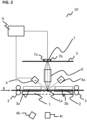
- FIG. 2 is a schematic representation of a device 10 for improving the reproducibility of recordings according to various embodiments.
- the device 10 for improving the reproducibility of recordings comprises a guide device 1 which is set up to guide at least one object 2 in the object plane 1a, at least one drive device 3 which is set up to transport the object 2 on the guide device 1 in the object plane 1a in a transport direction 8, at least one light source 4 for illuminating the object 2, an image plane 5, a plurality of rod lenses 6 which are arranged between the object plane 1a and the image plane 5 and in a row along a direction transverse to the transport direction 8 of the object 2, at least one light-sensitive line pixel array 7 of a contact image sensor which is arranged in the image plane 5, a control device 9 which is set up to control at least the light source 4 and/or the line pixel array 7 and to detect a signal generated by the line pixel array, wherein a light emitted by the light source 4 is at least partially scattered from the object 2 towards the rod lenses 6.
- each line pixel array 7a, 7b has a length transverse to the transport direction 8 of the object 2 which completely covers the object 2 to be detected.
- An object 2, for example a check or a banknote, can be transported from a first side by means of the drive device 3 along the object plane 1a or also in the opposite direction (bidirectional).
- the drive device 3 can have a plurality of rollers that can transport an object 2 in or against the transport direction 8. At least one roller can be driven by a motor.
- the device 10 can have a plurality of light sources 4, 4a, 4b, 4c, 4d. At least one light source can be used for incident light operation, for example the light sources 4 and 4a. At least one light source can be used for transmitted light operation, for example the light sources 4b and 4c. While the object 2 moves along the transport direction 8 at a predefined speed, the light sources 4, 4a emit at least one light with one or more defined wavelengths.
- the emitted light is partially absorbed by the object 2 located underneath and partially scattered or reflected in a direction towards the rod lenses 6.
- the light sources 4, 4a can be rod-shaped so that the light illuminates a strip of the object almost simultaneously.
- a portion of the scattered or reflected light is Rod lenses 6 are optically imaged onto the image plane 5 and a part falls onto the two adjacently arranged one-dimensional line pixel arrays 7a, 7b, as is exemplified in the FIG. 2 is shown.
- the device 10 shown may comprise a light source 4.
- at least one light source 4, 4a can be arranged at different angles to the object plane.
- the light source 4, 4a can be positioned at an angle to the object plane 1a in a value range of about 10 degrees to about 80 degrees, for example in a value range of about 15 degrees to about 75 degrees, for example at an angle of about 45 degrees to the object plane 1a.
- the light source 4 can be arranged at an angle of about 50 degrees and the second light source 4a at an angle of about 60 degrees to the object plane 1a.
- the light sources 4 and 4a can be arranged symmetrically with respect to the plurality of rod lenses.
- Simultaneous illumination can make the illumination more diffuse, or angle-dependent scattering can be evaluated by time multiplexing.
- the device 10 can be operated by means of incident light using at least the light source 4 and/or 4a.
- the device 10 can also be operated by means of a transmitted light mode, for example a bright field mode and/or a dark field mode.
- the device 10 can, for example, operate a light source 4b in a dark field transmitted light mode.
- the device 10 can, for example, operate a light source 4c in a bright field transmitted light mode.
- the light sources 4b, 4c can be arranged on a different side in relation to the object plane 1a compared to at least one of the light sources 4, 4a.
- the light source 4c can, for example, when operated as a bright field light source, be arranged on an optical axis of a rod lens 6, for example approximately below the FIG. 2
- the light source 4b can be arranged adjacent to the light source 4c and on the same side with respect to the object plane 1a.
- At least one of the light sources 4, 4a, 4b, 4c can be operated by means of time-multiplex illumination.
- the time-multiplex illumination method can be carried out with respect to a wavelength of illumination and/or between incident and transmitted light and/or with respect to an illumination angle.
- the control device 9 can operate the light sources 4 and 4a for a 940 nanometer (nm) incident light line simultaneously.
- the control device can, for example, also operate the light source 4c for a 940 nm transmitted light line
- the object can be illuminated with the color blue
- the object can be illuminated with green
- the object can be illuminated with red
- the object can be irradiated with infrared.
- the two rows 7a, 7b of the light-sensitive line pixel array 7, for example CMOS rows can measure at least one pixel value and the control device 9 can receive and export data in analog or digital form.
- the control device 9 can be housed in the device 10 or arranged decentrally.
- the guide device 1 can be transparent in a partial area, for example translucent, for example in a transmitted light operation of the device 10.
- the device 10 can further comprise guides 3a and 3b for guiding an object 2.
- the guides 3a and 3b can be arranged opposite to the guide device 1 in relation to an object 2.
- the guides 3a can be transparent in at least a partial area, for example translucent, for example in a transmitted light operation of the device 10, as shown schematically in the FIG. 2 In the area of the illumination and/or the optical imaging, parts of the guide device may be missing in order to enable the illumination and/or the optical imaging.
- the control device 9 is designed to operate the first line pixel array 7a and the second line pixel array 7b independently of one another and to connect the second line pixel array 7b to the first line pixel array 7a and vice versa.
- the majority of the line pixel arrays 7a, 7b have, for example, a resolution in the direction transverse to the transport direction 8 of 200 dpi.
- a pixel of the majority of line pixel arrays 7a, 7b can have a size of 127 micrometers by 127 micrometers.
- the control device 9 is configured, in a case where the object 2 is at least a check, to set a resolution of the first line pixel array 7a to 200 dpi, to deactivate the second line pixel array 7b, to control the first line pixel array 7a, and to read out the pixel values of the first line pixel array 7a.
- the control device 9 is further configured, in a case where the object 2 is at least one banknote, to set a resolution of the first line pixel array 7a and the second line pixel array 7b to 100 dpi, to activate the first and the second line pixel array 7a, 7b, to read out and summarize at least two pixel values of neighboring pixels 7a_1, 7a_2 in the first line pixel array 7a, to read out and summarize at least two pixel values of neighboring pixels 7b_1, 7b_2 corresponding to the two neighboring pixels 7a_1, 7a_2 in the first line pixel array 7a in the second line pixel array 7b, to summarize the two summarized neighboring pixels 7a_1, 7a_2 in the first line pixel array 7a and the two summarized neighboring pixels 7b_1, 7b_2 in the second line pixel array 7b, and provide a pixel value based on the aggregated pixel values for further processing.
- the control device 9 is further configured to combine pixel values of two adjacent pixels 7a_1, 7a_2 of the first line pixel array 7a and pixel values of two adjacent pixels 7b_1, 7b_2 of the second line pixel array 7b, which correspond to the two adjacent pixels 7a_1, 7a_2 of the first line pixel array 7a, by means of an analog 2x2 binning method, and to provide a pixel value based on the combined pixel values for further processing.
- the control device 9 is further configured to activate the first and second line pixel arrays 7a, 7b, to read out at least a first pixel value of a first pixel 7a_1 of the first line pixel array 7a and a first pixel value of a first pixel 7b_1 of the second line pixel array 7b, to read out at least a second pixel value of the second pixel 7a_2 of the first line pixel array 7a and a second pixel value of the second pixel 7b_2 of the second line pixel array 7b, and to calculate a mean value from the first pixel values and the second pixel values using a line averaging acquisition method and to provide a pixel value for further processing.
- the second light source 4a can be arranged as a reflected light source to the light source 4 in a mirrored manner with respect to a plane that runs perpendicular to the object plane 1, parallel to the rod lenses 6 and runs through a central optical axis of the rod lenses 6.
- the reflected light source 4a can be provided in such a way that it can be positioned at different angles to an object guide 1, for example in a value range of approximately 30 degrees to approximately 60 degrees, for example at an angle of approximately 45 degrees.
- at least a transmitted light source 4b, 4c can be provided.
- at least one light source can be operated as a transmitted light source.
- the transmitted light source can be arranged on an opposite side to the image plane with respect to a guide device 1.
- the device 10 has a row of rod lenses 6 or a plurality of rows of rod lenses 6 arranged in a row, wherein the rows of rod lenses 6 are arranged parallel to one another, and wherein the rows are each arranged transversely to the transport device 8.
- At least a first row of the plurality of rows of rod lenses 6 can be arranged adjacent to at least one further row of the plurality of rod lenses, wherein the first row of rod lenses 6 and the further row of rod lenses can be arranged in a direction transverse to the transport direction of the object 2 at a predefined distance from one another, for example in a value range of approximately 1 micrometer to 10 micrometers, for example at a distance of 2 micrometers, for example 4 micrometers, for example 7 micrometers, for example 9 micrometers, and can be arranged displaced from one another by a predefined distance, for example in a value range of approximately 0 micrometers to approximately 400 micrometers, for example 130 micrometers to approximately 340 micrometers, for example at a distance of approximately 190 micrometers, transverse to the transport direction 8, and/or at least one gap between a rod lens 6 and an adjacent rod lens can be filled with at least one filling material, for example black silicon wax or black silicon resin. be filled up.
- at least one filling material
- the device described herein can be operated by means of a method described herein for improving the reproducibility of recordings.
- the method can comprise: at least one of guiding at least one object 2 on a guide device 1 in an object plane 1a by means of the guide device 1, transporting the object 2 on the guide device 1 in the object plane 1a in a transport direction 8 by means of at least one drive device 3, illuminating the object 2 by means of at least one light source 4, at least partially scattering a light emitted by the light source 4 from the object 2 to the rod lenses 6, forwarding at least a portion of the light scattered by the object 2 by means of a plurality of rod lenses 6 which are arranged between the object plane 1a and an image plane 5 and are arranged in a row along a direction transverse to the transport direction 8 of the object 2, to form a light-sensitive line pixel array 7, controlling at least the light source 4 and/or the light-sensitive line pixel array 7 by means of a control device 9, wherein the light-sensitive line pixel array 7 has a plurality
- the transport direction 8 can also be in a direction to that in FIG. 2
- the device 10 can also be configured to transport the object 2 both in a first transport direction 8 and in a second transport direction that is opposite to the first transport direction.
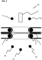
- FIG. 3 is a schematic representation of a device 20 for improving the reproducibility of recordings according to various embodiments.
- the information relating to the FIG. 3 Device 20 described may have at least one feature or all features of the device described with respect to the FIG. 2 described device 10.
- the device described in the FIG. 3 illustrated reference numerals corresponding reference numerals which, in relation to the FIG. 2 be used.
- the device 20 in FIG. 3 has a plurality of light sources 4, 4a, 4b, 4c and 4d.
- a banknote or a check can be transported, for example, by means of a plurality of belts, as is shown for example in the FIG. 3
- the device 20 can be operated, for example, in a reflected light mode, in which at least one light source 4, 4a is operated to illuminate at least one object 2 which is in the Device 20 can be transported.
- the device 20 can be operated, for example, in a transmitted light mode, in which at least one light source 4b, 4c, 4d is operated to illuminate the object 2.
- the light source 4b and/or 4d can be operated, for example, in a dark field transmitted light mode.
- the light source 4c can be operated, for example, in a bright field transmitted light mode.
- at least one light source 4, 4a can be arranged on the same side (incident light measurement) with respect to the object plane and/or at least one light source 4b, 4c, 4d can be on the opposite side (transmitted light measurement) as the image plane.
- the arrangements of the light sources 4, 4a, 4b, 4c, 4d in the FIG. 3 illustrate a possible arrangement.
- the light sources 4, 4a, 4b, 4c, 4d can have other positions.
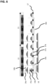
- FIG. 4A, FIG. 4B, FIG. 4C, FIG. 4D are schematic representations of a portion of a device and a method for improving the reproducibility of recordings according to various embodiments.
- the FIG. 4A, FIG. 4B, FIG. 4C and FIG. 4D each show a diagram that schematically illustrates a contact image sensor 10 with two one-dimensional line pixel arrays 7a, 7b according to various embodiments.
- the first line pixel array 7a has a plurality of pixels 7a_1, 7a_2.
- the second line pixel array 7b has a A plurality of pixels 7b_1, 7b_2.
- Each pixel of the plurality of pixels 7a_1, 7a_2, 7b_1, 7b_2 can be read out, for example, by means of the control device 9.
- FIG.4A shows a resting state of the contact image sensor 10 with two one-dimensional line pixel arrays 7a, 7b according to various embodiments.
- the Fig. 4B shows a first operating state (check operation) of the contact image sensor 10 with two one-dimensional line pixel arrays 7a, 7b according to various embodiments.
- the control device 9 is set up to set a resolution of the first line pixel array 7a to 200 dpi in a case where the object 2 is at least a check. Furthermore, the control device 9 deactivates the second line pixel array 7b.
- the control device 9 controls the first line pixel array 7a and reads out the pixel values of the first line pixel array 7a, for example in an intrinsic resolution.
- the FIG. 4C shows a second operating state (banknote operation) of the contact image sensor 10 with two one-dimensional line pixel arrays 7a, 7b according to various embodiments.
- the control device 9 is set up to set a resolution of the first line pixel array 7a and the second line pixel array 7b to 100 dpi in a case where the object 2 is at least one banknote.
- the control device 9 activates the first and the second line pixel array 7a, 7b and reads out at least two pixel values of neighboring pixels 7a_1, 7a_2 in the first line pixel array 7a and summarizes them.
- the control device 9 is further set up to read out and summarize at least two pixel values of neighboring pixels 7b_1, 7b_2 in the second line pixel array 7b that correspond to the two neighboring pixels 7a_1, 7a_2 in the first line pixel array 7a.
- the control device 9 is further configured to combine the two combined adjacent pixels 7a_1, 7a_2 in the first line pixel array 7a and the two combined adjacent pixels 7b_1, 7b_2 in the second line pixel array 7b, for example by means of a binning method, and to provide a pixel value based on the combined pixel values for further processing.
- control device 9 is further configured to combine pixel values of two adjacent pixels 7a_1, 7a_2 of the first line pixel array 7a and pixel values of two adjacent pixels 7b_1, 7b_2 of the second line pixel array 7b, which correspond to the two adjacent pixels 7a_1, 7a_2 of the first line pixel array 7a, using a 2x2 binning method and to provide a pixel value based on the combined pixel values for further processing.
- the control device operates the two lines at half resolution.
- the binning method enables a higher light sensitivity per virtual pixel and a signal-to-noise ratio can be improved and a line can be read out more quickly.
- control device 9 is further configured to activate the first and the second line pixel array 7a, 7b, to read out at least a first pixel value of a first pixel 7a_1 of the first line pixel array 7a and a first pixel value of a first pixel 7b_1 of the second line pixel array 7b.
- the control device 9 is further configured to read out at least a second pixel value of the second pixel 7a_2 of the first line pixel array 7a and a second pixel value of the second pixel 7b_2 of the second line pixel array 7b and to calculate an average value by means of a Line averaging acquisition method to calculate from the first pixel values and the second pixel values and to provide one pixel value each for further processing.
- the device and method for improving the reproducibility of images can enable one and the same contact image sensor with different resolutions to be operated with the same performance as a contact image sensor specifically designed for that resolution, without a significant increase in manufacturing costs due to higher quantities of that model.
- the resolution can be configured during operation without a loss of performance compared to a contact image sensor which is only designed for the corresponding resolution or with two differently designed contact image sensors, which increases the costs, space requirements and risk of jams. Such switching is necessary if the banknote reader must also be used for check operation and/or if color channels with different resolutions are operated in the lighting sequence.
- the control device 9 can switch between the Figures 4B and 4C described operating modes. For example, it can be determined that the object is a check. The control device 9 can then switch to the operating mode described in relation to the FIG. 4B described operating mode. For example, it can be determined that the object is at least one banknote. The control device 9 can then switch to the operating mode described with respect to the FIG. 4C described operating mode.
- the operating modes can also change within the color sequence.
- the individual pixel values can be read out and converted by means of an analog-digital converter 11, as described in the FIG. 4A to FIG. 4D is shown schematically.
- FIG.4D shows a further operating state of a contact image sensor with two one-dimensional line pixel arrays 7a, 7b according to various embodiments.
- at least one pixel in at least one line pixel array can be wider transversely to the transport direction than a pixel in at least one further line pixel array.
- a pixel in a first line pixel array can be wider in relation to a corresponding pixel in a second line pixel array by, for example, about a factor of 1.5 to about a factor of 3.5, for example by a factor of 2.
- a pixel width transversely to the transport direction of an object in a first line can be twice as wide in relation to a pixel width in a second line.
- a first pixel of a line can have a width transversely to the transport direction of an object that two pixels in an adjacent line together have transversely to the transport direction.
- a width transversely to the transport direction of a pixel in a first line pixel array 7a and of a pixel in a second line pixel array 7b can be, for example, 127 micrometers.
- a width transverse to the transport direction of a pixel in a first line pixel array 7a can be, for example, 127 micrometers and a width transverse to the transport direction of a pixel in a second line pixel array 7b can be, for example, 254 micrometers.
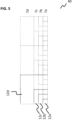
- FIG. 5 is a schematic representation of a partial region 40 of a device for improving the reproducibility of recordings according to various embodiments.
- FIG. 5 illustrates, by way of example, a partial area 40 of a moiré-free contact image sensor in 100, 200, 300 and 600 dots per inch resolution.
- a device 10, 20 for improving the reproducibility of recordings at least one pixel in at least one line pixel array can be made wider than a pixel in at least one further line pixel array.
- a first line has a plurality of pixels of the same size (see pixel sequence in line 7a in FIG. 5 ).
- An adjacent line has pixels of different widths, namely pixels that are twice as wide as pixels of the first line.
- a second line has a pixel sequence of: pixels with a pixel width of two pixels, pixels with a pixel width of one pixel of the first line, pixels with a pixel width of one pixel, pixels with a pixel width of two pixels (see pixel sequence in line 7b in FIG. 5 ).
- This sequence repeats in the second line.
- a pixel has a pixel width of: Pixel with pixel width of three pixels in the first line. This pixel width can repeat in the third line (see pixel sequence in line 7c in FIG. 5 ).
- a pixel can have a pixel width of six pixels of the first line. This width can be repeated in the fourth line (see pixel sequence in line 7d in FIG. 5 ).
- the height of the pixels in the fourth row can be three pixel heights of the pixels in the first row.
- a lower row 7a can be designed for 600 dots per inch, see 12a. If a resolution of 300 dots per inch is to be recorded, a pixel area can be enlarged to the pixel area 12b by means of an analog binning. If a resolution of 200 dots per inch is to be recorded, a pixel area can be enlarged to a pixel area 12c by means of an analog binning. If a resolution of 100 dots per inch is to be recorded, a pixel area can be enlarged to a pixel area 12d by means of an analog binning. In other words, pixels can be combined in such a way that at least one larger pixel can be created.
- a plurality of pixels in at least one row or in a plurality of rows can be combined in such a way that a respective resolution, for example 100 dots per inch, can be realized.
- a respective resolution for example 100 dots per inch
- two adjacent pixels can be connected together in a first row and corresponding pixels can be connected together in a second row (see 12b), which in turn can be connected together as shown schematically in the FIG. 5
- the pixel area 12b, 12c, 12d shown can be individually connected or combined using an analog binning process.
- FIG. 6 is a schematic representation of a portion of a device and a method for improving the reproducibility of recordings according to various embodiments.
- the FIG. 6 illustrates an illumination sequence in which a contact image sensor can be designed for a resolution of 200 dpi, for example.
- the FIG. 6 Contact Image Sensor illustrated may be, for example, a Contact Image Sensor described herein.
- the paths 13 in the FIG. 6 can have a length of about 1016 micrometers.
- a pitch, ie a step size between neighboring pixels transverse to the transport direction can be, for example, about 127 micrometers in the one-dimensional pixel array 7a, 7b.
- An extension of a pixel in the transport direction 8 cannot then exceed 127 micrometers, otherwise the resolution in the transport direction would become worse. This means that in the transport direction 8 the pixel 7a instantly captures 127 micrometers if the rod lens 6 could image perfectly.
- the distance 14a for example with a length of about 127 micrometers, represents a distance at a time when at least one of the light sources 4, 4a, 4b, 4c, 4d, for example an LED, is switched on.
- the object 2 moves in the transport direction 8.
- the recording location is shifted by approximately 1016 micrometers divided by 12 (see the line 14b in FIG. 6 ).
- the sensitivity of an ideal contact image sensor 10 and/or a line pixel array 7 in the transport direction 8 is given by the trapezoids A in the FIG. 6
- the pixel size in the transport direction 8 in a contact image sensor and/or in a light-sensitive line pixel array can effectively be only about 99 micrometers. Therefore, the distances 15a, 15b in FIG. 6 shorter.
- duty cycle is understood to be a ratio between the illumination duration and the inverse line rate.
- An inverse line rate can be understood as a line time, for example as 1,016 micrometers/(12*v), where v indicates a speed. Therefore, the sections 15a and 15b cover a smaller area than desired, or the flanks of the trapezoid B are steeper.
- the real sensitivity of, for example, a green channel in the transport direction 8 is determined by the trapezoids B in the FIG.
- a sensitivity of, for example, a green channel in the transport direction 8 as indicated by the trapezoids C in the FIG. 6 The gaps in sensitivity, as in trapezoids A and B in the FIG. 6 observed, have now practically disappeared.
- the second pixel in the transport direction 8 is somewhat longer than the first pixel in the transport direction 8, for example by a factor in a range from about 1.5 to about 1.7, for example by a factor of about 1.57, the sensitivity over the transport path 8 (or over the banknote) can be approximately constant. This means that a moiré effect can no longer occur.
- FIG. 7 is a flow chart schematically illustrating a method for improving the reproducibility of recordings according to various embodiments.
- the method for improving the reproducibility of recordings can comprise at least one of the following: guiding at least one object in an object plane by means of a guide device (S701); transporting the object in the object plane in a transport direction by means of at least one drive device (S702); illuminating the object by means of at least one light source of a contact image sensor (S703); at least partially scattering a light emitted by the light source from the object to a plurality of rod lenses of the contact image sensor (S704); imaging at least a portion of the light scattered by the object by means of the plurality of rod lenses arranged between the object plane and an image plane and in a row along a direction transverse to the transport direction of the object to at least one light-sensitive line pixel array of the contact image sensor (S705); controlling at least the light source and/or the light-sensitive line pixel array by means of a control device (S706), wherein the light-sensitive line pixel array has a plurality of one-dimensional line pixel arrays, each of
- the method may further comprise features relating to the FIG. 1 , FIG. 2 , FIG. 3 , FIG. 4 , FIG. 5 and or FIG. 6
- the advantages described in relation to the embodiments of the device described herein also relate to the embodiments of the method described herein and vice versa.
Landscapes
- Engineering & Computer Science (AREA)
- Multimedia (AREA)
- Signal Processing (AREA)
- Inspection Of Paper Currency And Valuable Securities (AREA)
- Image Input (AREA)
- Investigating Materials By The Use Of Optical Means Adapted For Particular Applications (AREA)
- Investigating Or Analysing Materials By Optical Means (AREA)
- Analysing Materials By The Use Of Radiation (AREA)
Claims (14)
- Dispositif d'amélioration de la reproductibilité des enregistrements comportant :un dispositif de guidage (1) qui est conçu pour guider au moins un objet (2) dans un plan objet (1a) ;au moins un dispositif d'entraînement (3) qui est conçu pour transporter l'objet (2) dans le plan objet (1a) dans une direction de transport (8),un plan image (5) ;au moins un capteur d'image de contact doté d'au moins une source lumineuse (4) pour éclairer l'objet (2),une pluralité de lentilles barreaux (6) qui sont disposées entre le plan objet (1a) et le plan image (5) et en une rangée le long d'une direction transversale à la direction de transport (8) de l'objet (2), etau moins un réseau de pixels de ligne (7) photosensible qui est disposé dans le plan image (5) ;un dispositif de commande (9) qui est conçu pour commander au moins la source lumineuse (4) et/ou le réseau de pixels de ligne (7) photosensible et pour détecter un signal généré par le réseau de pixels de ligne (7) photosensible,dans lequel une lumière émise par la source lumineuse (4) est au moins partiellement diffusée par l'objet (2) vers les lentilles barreaux (6), est mise sous forme d'image au moyen des lentilles barreaux (6) et est incidente sur au moins une zone du réseau de pixels de ligne (7) photosensible,dans lequel le réseau de pixels de ligne (7) photosensible comporte une pluralité de réseaux de pixels de lignes (7a, 7b) unidimensionnels, qui s'étendent respectivement le long de la direction transversale à la direction de transport (8) de l'objet (2), et sont disposés parallèlement les uns aux autres et côte à côte, dans lequel chaque réseau de pixels de ligne (7a, 7b) présente une longueur, transversalement à la direction de transport (8) de l'objet (2), qui couvre entièrement l'objet (2) à détecter, etdans lequel la pluralité de réseaux de pixels de lignes (7a, 7b) unidimensionnels comporte :- une première ligne de pixels de même taille,- une deuxième ligne adjacente à celle-ci d'une séquence répétitive de pixels ayant des largeurs de pixels mutuellement différentes transversalement à la direction de transport (8), qui comporte un pixel ayant la largeur de pixel de deux pixels de la première ligne, un pixel ayant la largeur de pixel d'un pixel de la première ligne, un pixel ayant la largeur de pixel d'un pixel de la première ligne et un pixel ayant la largeur de pixel de deux pixels de la première ligne, et qui chevauche six pixels de la première ligne,- une troisième ligne de pixels qui comporte des pixels ayant une largeur de trois pixels de la première ligne, de sorte que ceux-ci chevauchent respectivement depuis la deuxième ligne : un pixel ayant la largeur de pixel de deux pixels de la première ligne et un pixel ayant la largeur de pixel d'un pixel de la première ligne.
- Dispositif selon la revendication 1, dans lequel chaque réseau de pixels de ligne (7a, 7b) comporte une pluralité de pixels (7a_1, 7a_2, 7b_1, 7b_2), et chaque pixel (7a_1, 7a_2, 7b_1, 7b_2) comporte au moins une photodiode de type CMOS ou CCD pour détecter une valeur de pixel de la lumière émise par la source lumineuse (4), et/ou dans lequel un nombre des réseaux de pixels de lignes (7a, 7b) est inférieur à un nombre des pixels (7a_1, 7a_2 ; 7b_1, 7b_2) dans chaque réseau de pixels de lignes (7a ; 7b).
- Dispositif selon la revendication 1 ou 2, dans lequel des pixels provenant de différentes lignes peuvent être combinés au moyen d'un fusionnement analogique de telle sorte que des résolutions différentes peuvent être mises en œuvre.
- Dispositif selon l'une des revendications précédentes, dans lequel le dispositif de commande (9) est en outre conçu pour attaquer la première ligne (7a) et la deuxième ligne (7b) indépendamment l'une de l'autre, et dans lequel le dispositif de commande (9) est conçu pour connecter la deuxième ligne (7b) à la première ligne (7a).
- Dispositif selon l'une des revendications précédentes, dans lequel les pixels de la première ligne présentent une résolution de 600 dpi dans la direction transversale à la direction de transport (8),- et, lorsqu'une résolution de 300 dpi doit être détectée, sont combinés au moyen d'un fusionnement analogique en une surface de pixels (12b) qui comporte des pixels de la deuxième ligne ;- et, lorsqu'une résolution de 200 dpi doit être détectée, sont combinés au moyen d'un fusionnement analogique en une surface de pixels (12c) qui comporte des pixels des deuxième et troisième lignes.
- Dispositif selon l'une des revendications précédentes, dans lequel un pixel de la pluralité de réseaux de pixels de lignes (7a, 7b) présente une taille de 127 micromètres par 127 micromètres.
- Dispositif selon l'une des revendications précédentes, dans lequel la pluralité de réseaux de pixels de lignes (7a, 7b) unidimensionnels comporte une quatrième ligne de pixels ayant une largeur de pixel de six pixels de la première ligne, qui chevauchent respectivement deux pixels de la troisième ligne.
- Dispositif selon la revendication 7, dans lequel la quatrième ligne présente une résolution de 100 dpi dans la direction transversale à la direction de transport (8) et, lorsqu'une résolution de 100 dpi doit être détectée, est combinée au moyen d'un fusionnement analogique en une surface de pixels (12d) qui comporte des pixels des deuxième, troisième et quatrième lignes.
- Dispositif selon l'une des revendications 1 à 6, dans lequel le dispositif de commande (9) est en outre conçupour combiner des valeurs de pixels de deux pixels adjacents (7a_1, 7a_2) de la première ligne (7a) et au moins une valeur de pixel d'un pixel adjacent (7b_1, 7b_2) de la deuxième ligne (7b) au moyen d'un procédé de fusion analogique, etpour fournir une valeur de pixel sur la base des valeurs de pixels combinées en vue d'un traitement ultérieur.
- Dispositif selon l'une des revendications précédentes, dans lequel le dispositif de commande (9) est en outre conçupour activer les première et deuxième lignes (7a, 7b),pour lire au moins une première valeur de pixel d'un premier pixel (7a_1) des premières lignes (7a) et une première valeur de pixel d'un premier pixel (7b_1) des deuxièmes lignes (7b),pour lire au moins une deuxième valeur de pixel du deuxième pixel (7a_2) de la première ligne (7a) et une deuxième valeur de pixel du deuxième pixel (7b_2) des deuxièmes réseaux de lignes (7b),et pour calculer respectivement une valeur moyenne au moyen d'un procédé d'acquisition de moyenne de ligne à partir des premières valeurs de pixels et des deuxièmes valeurs de pixels et pour fournir respectivement une valeur de pixel en vue d'un traitement ultérieur.
- Dispositif selon l'une des revendications précédentes, dans lequel le dispositif (10) comporte au moins une deuxième source lumineuse (4a) pour éclairer l'objet (2), dans lequel la deuxième source lumineuse (4a) est disposée sur un côté opposé à la source lumineuse (4) par rapport à la pluralité de lentilles barreaux (6), et/ou les lentilles barreaux (6) sont des lentilles barreaux à gradient d'indice.
- Dispositif selon l'une des revendications précédentes, dans lequel le dispositif (10) comporte une pluralité de rangées de lentilles barreaux (6) disposées en rangée,dans lequel les rangées de lentilles barreaux (6) sont disposées parallèlement les unes aux autres, etdans lequel les rangées sont respectivement disposées transversalement par rapport au dispositif de transport (8) .
- Dispositif selon la revendication 12, dans lequel au moins une première rangée de la pluralité de rangées de lentilles barreaux (6) est disposée de manière adjacente à au moins une autre rangée de la pluralité de lentilles barreaux,dans lequel la première rangée de lentilles barreaux (6) et l'autre rangée de lentilles barreaux sont disposées à une distance prédéfinie l'une de l'autre dans une direction transversale à la direction de transport de l'objet (2) et sont disposées de manière décalée l'une par rapport à l'autre d'une distance prédéfinie transversalement à la direction de transport (8), et/ouau moins un espace intermédiaire entre une lentille barreau (6) et une lentille barreau (6) adjacente est rempli d'au moins un matériau de remplissage.
- Procédé d'amélioration de la reproductibilité des enregistrements, le procédé comprenant :la guidage d'au moins un objet (2) dans un plan objet (1a) au moyen d'un dispositif de guidage (1) ;le transport de l'objet (2) dans le plan objet (1a) dans une direction de transport (8) au moyen d'au moins un dispositif d'entraînement (3) ;l'éclairage de l'objet (2) au moyen d'au moins une source lumineuse (4) d'un capteur d'image de contact ;la diffusion au moins partielle d'une lumière émise par la source lumineuse (4) depuis l'objet (2) vers une pluralité de lentilles barreaux (6) du capteur d'image de contact ;la formation d'image d'au moins une partie de la lumière diffusée par l'objet (2) au moyen de la pluralité de lentilles barreaux (6) disposées entre le plan objet (1a) et un plan image (5) et en une rangée le long d'une direction transversale à la direction de transport (8) de l'objet (2), vers au moins un réseau de pixels de ligne (7) photosensible du capteur d'image de contact ;la commande d'au moins la source lumineuse (4) et/ou du réseau de pixels de ligne (7) photosensible au moyen d'un dispositif de commande (9),dans lequel le réseau de pixels de ligne (7) photosensible comporte une pluralité de réseaux de pixels de lignes (7a, 7b) unidimensionnels, qui s'étendent respectivement le long de la direction transversale à la direction de transport (8) de l'objet (2), et sont disposés parallèlement les uns aux autres et côté à côté, etdans lequel chaque réseau de pixels de ligne (7a, 7b) présente une longueur, transversalement à la direction de transport (8) de l'objet (2), qui couvre entièrement l'objet (2) à détecter,la détection d'au moins une partie de la lumière mise sous forme d'image par les lentilles barreaux (6) au moyen d'au moins une zone d'un réseau de pixels de ligne (7) photosensible qui est disposé dans le plan image (5), etla combinaison d'au moins certaines valeurs de pixels individuelles de la pluralité de réseaux de pixels de lignes (7a, 7b) unidimensionnels et la fourniture d'une valeur de pixel en vue d'un traitement ultérieur au moyen du dispositif de commande (9),dans lequel la pluralité de réseaux de pixels de lignes (7a, 7b) unidimensionnels comporte :- une première ligne de pixels de même taille,- une deuxième ligne adjacente à celle-ci d'une séquence répétitive de pixels ayant des largeurs de pixels mutuellement différentes transversalement à la direction de transport (8), qui comporte un pixel ayant la largeur de pixel de deux pixels de la première ligne, un pixel ayant la largeur de pixel d'un pixel de la première ligne, un pixel ayant la largeur de pixel d'un pixel de la première ligne et un pixel ayant la largeur de pixel de deux pixels de la première ligne, et qui chevauche six pixels de la première ligne,- une troisième ligne de pixels qui comporte des pixels ayant une largeur de trois pixels de la première ligne, de sorte que ceux-ci chevauchent respectivement depuis la deuxième ligne : un pixel ayant la largeur de pixel de deux pixels de la première ligne et un pixel ayant la largeur de pixel d'un pixel de la première ligne.
Priority Applications (5)
| Application Number | Priority Date | Filing Date | Title |
|---|---|---|---|
| EP21152490.5A EP4033744B1 (fr) | 2021-01-20 | 2021-01-20 | Dispositif et procédé d'amélioration de la reproductibilité des enregistrements |
| MX2023008477A MX2023008477A (es) | 2021-01-20 | 2022-01-19 | Dispositivo y metodo para mejorar la reproducibilidad de capturas de imágenes. |
| PCT/EP2022/051087 WO2022157174A1 (fr) | 2021-01-20 | 2022-01-19 | Dispositif et procédé pour améliorer la reproductibilité d'enregistrements |
| KR1020237027916A KR20230135618A (ko) | 2021-01-20 | 2022-01-19 | 레코딩들의 재현성을 개선하기 위한 디바이스 및 방법 |
| US18/273,374 US12531956B2 (en) | 2021-01-20 | 2022-01-19 | Device and method for improving the reproducibility of recordings |
Applications Claiming Priority (1)
| Application Number | Priority Date | Filing Date | Title |
|---|---|---|---|
| EP21152490.5A EP4033744B1 (fr) | 2021-01-20 | 2021-01-20 | Dispositif et procédé d'amélioration de la reproductibilité des enregistrements |
Publications (2)
| Publication Number | Publication Date |
|---|---|
| EP4033744A1 EP4033744A1 (fr) | 2022-07-27 |
| EP4033744B1 true EP4033744B1 (fr) | 2024-05-08 |
Family
ID=74194533
Family Applications (1)
| Application Number | Title | Priority Date | Filing Date |
|---|---|---|---|
| EP21152490.5A Active EP4033744B1 (fr) | 2021-01-20 | 2021-01-20 | Dispositif et procédé d'amélioration de la reproductibilité des enregistrements |
Country Status (5)
| Country | Link |
|---|---|
| US (1) | US12531956B2 (fr) |
| EP (1) | EP4033744B1 (fr) |
| KR (1) | KR20230135618A (fr) |
| MX (1) | MX2023008477A (fr) |
| WO (1) | WO2022157174A1 (fr) |
Families Citing this family (1)
| Publication number | Priority date | Publication date | Assignee | Title |
|---|---|---|---|---|
| EP4033744B1 (fr) * | 2021-01-20 | 2024-05-08 | CI Tech Sensors AG | Dispositif et procédé d'amélioration de la reproductibilité des enregistrements |
Family Cites Families (14)
| Publication number | Priority date | Publication date | Assignee | Title |
|---|---|---|---|---|
| JPS6434050A (en) * | 1987-07-29 | 1989-02-03 | Canon Kk | Line sensor for reading color |
| US6047886A (en) * | 1998-01-06 | 2000-04-11 | Cash Code Company Inc. | Validator with replaceable sensor module |
| US6320680B1 (en) * | 1998-06-18 | 2001-11-20 | Digimarc Corporation | Stochastic scanning documents to change moire effects |
| TW475330B (en) * | 1999-10-29 | 2002-02-01 | Hewlett Packard Co | Photosensor array with multiple different sensor areas |
| US6894812B1 (en) * | 2000-10-31 | 2005-05-17 | Hewlett-Packard Development Company, L.P. | Photosensor assembly with shared structures |
| US6961157B2 (en) * | 2001-05-29 | 2005-11-01 | Xerox Corporation | Imaging apparatus having multiple linear photosensor arrays with different spatial resolutions |
| JP2003202516A (ja) * | 2001-12-28 | 2003-07-18 | Nippon Sheet Glass Co Ltd | 画像形成装置 |
| US6891146B2 (en) * | 2002-07-30 | 2005-05-10 | Hewlett-Packard Development Company, L.P. | Photosensor assembly with shared charge transfer registers |
| JP2004302150A (ja) * | 2003-03-31 | 2004-10-28 | Fuji Photo Optical Co Ltd | 画像読取装置 |
| JP4066960B2 (ja) * | 2004-01-28 | 2008-03-26 | 三菱電機株式会社 | イメージセンサ |
| US7359093B2 (en) * | 2004-05-14 | 2008-04-15 | Xerox Corporation | Systems and methods for streak detection in image array scanning using overdetermined scanners and column filtering |
| JP2012249237A (ja) * | 2011-05-31 | 2012-12-13 | Kyocera Document Solutions Inc | 画像読取装置及びこれを備えた画像形成装置 |
| JP6589420B2 (ja) * | 2015-07-10 | 2019-10-16 | 富士ゼロックス株式会社 | 補正制御装置、画像読取装置、補正制御プログラム |
| EP4033744B1 (fr) * | 2021-01-20 | 2024-05-08 | CI Tech Sensors AG | Dispositif et procédé d'amélioration de la reproductibilité des enregistrements |
-
2021
- 2021-01-20 EP EP21152490.5A patent/EP4033744B1/fr active Active
-
2022
- 2022-01-19 US US18/273,374 patent/US12531956B2/en active Active
- 2022-01-19 KR KR1020237027916A patent/KR20230135618A/ko active Pending
- 2022-01-19 WO PCT/EP2022/051087 patent/WO2022157174A1/fr not_active Ceased
- 2022-01-19 MX MX2023008477A patent/MX2023008477A/es unknown
Also Published As
| Publication number | Publication date |
|---|---|
| US20240121348A1 (en) | 2024-04-11 |
| MX2023008477A (es) | 2023-09-18 |
| KR20230135618A (ko) | 2023-09-25 |
| WO2022157174A1 (fr) | 2022-07-28 |
| EP4033744A1 (fr) | 2022-07-27 |
| US12531956B2 (en) | 2026-01-20 |
Similar Documents
| Publication | Publication Date | Title |
|---|---|---|
| EP0537431B1 (fr) | Dispositif pour la reconnaissance optique de documents | |
| DE69515445T2 (de) | Verfahren und Vorrichtung zum Kennzeichnen und Unterscheiden von Banknoten und legalen Zahlungsmitteln | |
| EP0824736B1 (fr) | Dispositif et procede pour le controle d'objets sous forme de feuilles tels que des billets de banque ou des titres | |
| EP1805978B1 (fr) | Dispositif de balayage pour la mesure photoélectrique d'un objet à mesurer | |
| DE69304816T2 (de) | Verfahren und Gerät zum Nachweis von Fehlern in durchsichtigem Bahnmaterial sowie Glasfolien | |
| DE60026201T2 (de) | Abtastverfahren für einen Fotosensor mit mehreren verschieden großen Abtastflächen | |
| DE69329186T2 (de) | Bildlesevorrichtung | |
| DE3586271T2 (de) | Handgefuehrte abtastvorrichtung. | |
| DE69629235T2 (de) | Gerät zur automatischen Detektion der Anwesenheit, der Breite und der Phasenverschiebung eines Dokumentes innerhalb eines Dokumentenabtasters | |
| EP1180898A1 (fr) | Méthode et dispositif pour la mesure colorimétrique d'un document bidimensionnel | |
| DE3246895A1 (de) | Vorlagen-bildunterscheidungsvorrichtung | |
| DE102005031490A1 (de) | Kostengünstige multi-sensorielle Oberflächeninspektion | |
| DE3913455A1 (de) | Farbbildabtaster | |
| DE68923414T2 (de) | Selbstlaufender Abtaster zum optischen Lesen von Bildern. | |
| EP4033744B1 (fr) | Dispositif et procédé d'amélioration de la reproductibilité des enregistrements | |
| DE10000030A1 (de) | Kamerasystem für die Bearbeitung von Dokumenten | |
| DE3788545T2 (de) | Abbildungssystem mit einer oszillierenden Anordnung von Gradientenlinsen. | |
| DE2917253A1 (de) | Informationserfassungsvorrichtung | |
| DE69922741T2 (de) | Farbbildaufnahmevorrichtung und Bildleser der diese Farbbildaufnahmevorrichtung benutzt | |
| DE102004012029B4 (de) | Bilderfassungsvorrichtung, System mit derselben und Verfahren zum doppelseitigen Abtasten eines Objekts | |
| DE19528443A1 (de) | Verbesserte Y-Skalierung für Farbabtastgeräte unter Verwendung von linearen CCDs mit mehreren Streifen | |
| DE69512586T2 (de) | Bildaufnahmevorrichtung und Bildlesegerät damit | |
| DE102008025417A1 (de) | Verfahren zur Ermittlung von Parametern eines Druckprozesses | |
| DE102005004393B4 (de) | Zweidimensionales CMOS-Sensorarray zur Abbildung von Dokumenten und anderen flachen Objekten | |
| DE69711801T2 (de) | Positionsbestimmungselement und Abstandssensor |
Legal Events
| Date | Code | Title | Description |
|---|---|---|---|
| PUAI | Public reference made under article 153(3) epc to a published international application that has entered the european phase |
Free format text: ORIGINAL CODE: 0009012 |
|
| STAA | Information on the status of an ep patent application or granted ep patent |
Free format text: STATUS: THE APPLICATION HAS BEEN PUBLISHED |
|
| STAA | Information on the status of an ep patent application or granted ep patent |
Free format text: STATUS: REQUEST FOR EXAMINATION WAS MADE |
|
| AK | Designated contracting states |
Kind code of ref document: A1 Designated state(s): AL AT BE BG CH CY CZ DE DK EE ES FI FR GB GR HR HU IE IS IT LI LT LU LV MC MK MT NL NO PL PT RO RS SE SI SK SM TR |
|
| 17P | Request for examination filed |
Effective date: 20220630 |
|
| RBV | Designated contracting states (corrected) |
Designated state(s): AL AT BE BG CH CY CZ DE DK EE ES FI FR GB GR HR HU IE IS IT LI LT LU LV MC MK MT NL NO PL PT RO RS SE SI SK SM TR |
|
| STAA | Information on the status of an ep patent application or granted ep patent |
Free format text: STATUS: EXAMINATION IS IN PROGRESS |
|
| 17Q | First examination report despatched |
Effective date: 20220812 |
|
| GRAP | Despatch of communication of intention to grant a patent |
Free format text: ORIGINAL CODE: EPIDOSNIGR1 |
|
| STAA | Information on the status of an ep patent application or granted ep patent |
Free format text: STATUS: GRANT OF PATENT IS INTENDED |
|
| INTG | Intention to grant announced |
Effective date: 20231215 |
|
| GRAS | Grant fee paid |
Free format text: ORIGINAL CODE: EPIDOSNIGR3 |
|
| GRAA | (expected) grant |
Free format text: ORIGINAL CODE: 0009210 |
|
| STAA | Information on the status of an ep patent application or granted ep patent |
Free format text: STATUS: THE PATENT HAS BEEN GRANTED |
|
| AK | Designated contracting states |
Kind code of ref document: B1 Designated state(s): AL AT BE BG CH CY CZ DE DK EE ES FI FR GB GR HR HU IE IS IT LI LT LU LV MC MK MT NL NO PL PT RO RS SE SI SK SM TR |
|
| REG | Reference to a national code |
Ref country code: GB Ref legal event code: FG4D Free format text: NOT ENGLISH |
|
| REG | Reference to a national code |
Ref country code: CH Ref legal event code: EP |
|
| REG | Reference to a national code |
Ref country code: DE Ref legal event code: R096 Ref document number: 502021003625 Country of ref document: DE |
|
| REG | Reference to a national code |
Ref country code: IE Ref legal event code: FG4D Free format text: LANGUAGE OF EP DOCUMENT: GERMAN |
|
| REG | Reference to a national code |
Ref country code: LT Ref legal event code: MG9D |
|
| REG | Reference to a national code |
Ref country code: NL Ref legal event code: MP Effective date: 20240508 |
|
| PG25 | Lapsed in a contracting state [announced via postgrant information from national office to epo] |
Ref country code: IS Free format text: LAPSE BECAUSE OF FAILURE TO SUBMIT A TRANSLATION OF THE DESCRIPTION OR TO PAY THE FEE WITHIN THE PRESCRIBED TIME-LIMIT Effective date: 20240908 |
|
| PG25 | Lapsed in a contracting state [announced via postgrant information from national office to epo] |
Ref country code: BG Free format text: LAPSE BECAUSE OF FAILURE TO SUBMIT A TRANSLATION OF THE DESCRIPTION OR TO PAY THE FEE WITHIN THE PRESCRIBED TIME-LIMIT Effective date: 20240508 |
|
| PG25 | Lapsed in a contracting state [announced via postgrant information from national office to epo] |
Ref country code: FI Free format text: LAPSE BECAUSE OF FAILURE TO SUBMIT A TRANSLATION OF THE DESCRIPTION OR TO PAY THE FEE WITHIN THE PRESCRIBED TIME-LIMIT Effective date: 20240508 Ref country code: HR Free format text: LAPSE BECAUSE OF FAILURE TO SUBMIT A TRANSLATION OF THE DESCRIPTION OR TO PAY THE FEE WITHIN THE PRESCRIBED TIME-LIMIT Effective date: 20240508 |
|
| PG25 | Lapsed in a contracting state [announced via postgrant information from national office to epo] |
Ref country code: GR Free format text: LAPSE BECAUSE OF FAILURE TO SUBMIT A TRANSLATION OF THE DESCRIPTION OR TO PAY THE FEE WITHIN THE PRESCRIBED TIME-LIMIT Effective date: 20240809 |
|
| PG25 | Lapsed in a contracting state [announced via postgrant information from national office to epo] |
Ref country code: PT Free format text: LAPSE BECAUSE OF FAILURE TO SUBMIT A TRANSLATION OF THE DESCRIPTION OR TO PAY THE FEE WITHIN THE PRESCRIBED TIME-LIMIT Effective date: 20240909 |
|
| PG25 | Lapsed in a contracting state [announced via postgrant information from national office to epo] |
Ref country code: NL Free format text: LAPSE BECAUSE OF FAILURE TO SUBMIT A TRANSLATION OF THE DESCRIPTION OR TO PAY THE FEE WITHIN THE PRESCRIBED TIME-LIMIT Effective date: 20240508 |
|
| PG25 | Lapsed in a contracting state [announced via postgrant information from national office to epo] |
Ref country code: ES Free format text: LAPSE BECAUSE OF FAILURE TO SUBMIT A TRANSLATION OF THE DESCRIPTION OR TO PAY THE FEE WITHIN THE PRESCRIBED TIME-LIMIT Effective date: 20240508 |
|
| PG25 | Lapsed in a contracting state [announced via postgrant information from national office to epo] |
Ref country code: PL Free format text: LAPSE BECAUSE OF FAILURE TO SUBMIT A TRANSLATION OF THE DESCRIPTION OR TO PAY THE FEE WITHIN THE PRESCRIBED TIME-LIMIT Effective date: 20240508 |
|
| PG25 | Lapsed in a contracting state [announced via postgrant information from national office to epo] |
Ref country code: LV Free format text: LAPSE BECAUSE OF FAILURE TO SUBMIT A TRANSLATION OF THE DESCRIPTION OR TO PAY THE FEE WITHIN THE PRESCRIBED TIME-LIMIT Effective date: 20240508 |
|
| PG25 | Lapsed in a contracting state [announced via postgrant information from national office to epo] |
Ref country code: PT Free format text: LAPSE BECAUSE OF FAILURE TO SUBMIT A TRANSLATION OF THE DESCRIPTION OR TO PAY THE FEE WITHIN THE PRESCRIBED TIME-LIMIT Effective date: 20240909 Ref country code: PL Free format text: LAPSE BECAUSE OF FAILURE TO SUBMIT A TRANSLATION OF THE DESCRIPTION OR TO PAY THE FEE WITHIN THE PRESCRIBED TIME-LIMIT Effective date: 20240508 Ref country code: NO Free format text: LAPSE BECAUSE OF FAILURE TO SUBMIT A TRANSLATION OF THE DESCRIPTION OR TO PAY THE FEE WITHIN THE PRESCRIBED TIME-LIMIT Effective date: 20240808 Ref country code: NL Free format text: LAPSE BECAUSE OF FAILURE TO SUBMIT A TRANSLATION OF THE DESCRIPTION OR TO PAY THE FEE WITHIN THE PRESCRIBED TIME-LIMIT Effective date: 20240508 Ref country code: LV Free format text: LAPSE BECAUSE OF FAILURE TO SUBMIT A TRANSLATION OF THE DESCRIPTION OR TO PAY THE FEE WITHIN THE PRESCRIBED TIME-LIMIT Effective date: 20240508 Ref country code: IS Free format text: LAPSE BECAUSE OF FAILURE TO SUBMIT A TRANSLATION OF THE DESCRIPTION OR TO PAY THE FEE WITHIN THE PRESCRIBED TIME-LIMIT Effective date: 20240908 Ref country code: HR Free format text: LAPSE BECAUSE OF FAILURE TO SUBMIT A TRANSLATION OF THE DESCRIPTION OR TO PAY THE FEE WITHIN THE PRESCRIBED TIME-LIMIT Effective date: 20240508 Ref country code: GR Free format text: LAPSE BECAUSE OF FAILURE TO SUBMIT A TRANSLATION OF THE DESCRIPTION OR TO PAY THE FEE WITHIN THE PRESCRIBED TIME-LIMIT Effective date: 20240809 Ref country code: FI Free format text: LAPSE BECAUSE OF FAILURE TO SUBMIT A TRANSLATION OF THE DESCRIPTION OR TO PAY THE FEE WITHIN THE PRESCRIBED TIME-LIMIT Effective date: 20240508 Ref country code: ES Free format text: LAPSE BECAUSE OF FAILURE TO SUBMIT A TRANSLATION OF THE DESCRIPTION OR TO PAY THE FEE WITHIN THE PRESCRIBED TIME-LIMIT Effective date: 20240508 Ref country code: BG Free format text: LAPSE BECAUSE OF FAILURE TO SUBMIT A TRANSLATION OF THE DESCRIPTION OR TO PAY THE FEE WITHIN THE PRESCRIBED TIME-LIMIT Effective date: 20240508 Ref country code: RS Free format text: LAPSE BECAUSE OF FAILURE TO SUBMIT A TRANSLATION OF THE DESCRIPTION OR TO PAY THE FEE WITHIN THE PRESCRIBED TIME-LIMIT Effective date: 20240808 |
|
| PG25 | Lapsed in a contracting state [announced via postgrant information from national office to epo] |
Ref country code: DK Free format text: LAPSE BECAUSE OF FAILURE TO SUBMIT A TRANSLATION OF THE DESCRIPTION OR TO PAY THE FEE WITHIN THE PRESCRIBED TIME-LIMIT Effective date: 20240508 |
|
| PG25 | Lapsed in a contracting state [announced via postgrant information from national office to epo] |
Ref country code: EE Free format text: LAPSE BECAUSE OF FAILURE TO SUBMIT A TRANSLATION OF THE DESCRIPTION OR TO PAY THE FEE WITHIN THE PRESCRIBED TIME-LIMIT Effective date: 20240508 |
|
| PG25 | Lapsed in a contracting state [announced via postgrant information from national office to epo] |
Ref country code: CZ Free format text: LAPSE BECAUSE OF FAILURE TO SUBMIT A TRANSLATION OF THE DESCRIPTION OR TO PAY THE FEE WITHIN THE PRESCRIBED TIME-LIMIT Effective date: 20240508 |
|
| PG25 | Lapsed in a contracting state [announced via postgrant information from national office to epo] |
Ref country code: SK Free format text: LAPSE BECAUSE OF FAILURE TO SUBMIT A TRANSLATION OF THE DESCRIPTION OR TO PAY THE FEE WITHIN THE PRESCRIBED TIME-LIMIT Effective date: 20240508 Ref country code: RO Free format text: LAPSE BECAUSE OF FAILURE TO SUBMIT A TRANSLATION OF THE DESCRIPTION OR TO PAY THE FEE WITHIN THE PRESCRIBED TIME-LIMIT Effective date: 20240508 |
|
| PG25 | Lapsed in a contracting state [announced via postgrant information from national office to epo] |
Ref country code: SM Free format text: LAPSE BECAUSE OF FAILURE TO SUBMIT A TRANSLATION OF THE DESCRIPTION OR TO PAY THE FEE WITHIN THE PRESCRIBED TIME-LIMIT Effective date: 20240508 |
|
| PG25 | Lapsed in a contracting state [announced via postgrant information from national office to epo] |
Ref country code: SM Free format text: LAPSE BECAUSE OF FAILURE TO SUBMIT A TRANSLATION OF THE DESCRIPTION OR TO PAY THE FEE WITHIN THE PRESCRIBED TIME-LIMIT Effective date: 20240508 Ref country code: SK Free format text: LAPSE BECAUSE OF FAILURE TO SUBMIT A TRANSLATION OF THE DESCRIPTION OR TO PAY THE FEE WITHIN THE PRESCRIBED TIME-LIMIT Effective date: 20240508 Ref country code: RO Free format text: LAPSE BECAUSE OF FAILURE TO SUBMIT A TRANSLATION OF THE DESCRIPTION OR TO PAY THE FEE WITHIN THE PRESCRIBED TIME-LIMIT Effective date: 20240508 Ref country code: EE Free format text: LAPSE BECAUSE OF FAILURE TO SUBMIT A TRANSLATION OF THE DESCRIPTION OR TO PAY THE FEE WITHIN THE PRESCRIBED TIME-LIMIT Effective date: 20240508 Ref country code: DK Free format text: LAPSE BECAUSE OF FAILURE TO SUBMIT A TRANSLATION OF THE DESCRIPTION OR TO PAY THE FEE WITHIN THE PRESCRIBED TIME-LIMIT Effective date: 20240508 Ref country code: CZ Free format text: LAPSE BECAUSE OF FAILURE TO SUBMIT A TRANSLATION OF THE DESCRIPTION OR TO PAY THE FEE WITHIN THE PRESCRIBED TIME-LIMIT Effective date: 20240508 |
|
| PG25 | Lapsed in a contracting state [announced via postgrant information from national office to epo] |
Ref country code: IT Free format text: LAPSE BECAUSE OF FAILURE TO SUBMIT A TRANSLATION OF THE DESCRIPTION OR TO PAY THE FEE WITHIN THE PRESCRIBED TIME-LIMIT Effective date: 20240508 |
|
| REG | Reference to a national code |
Ref country code: DE Ref legal event code: R097 Ref document number: 502021003625 Country of ref document: DE |
|
| PLBE | No opposition filed within time limit |
Free format text: ORIGINAL CODE: 0009261 |
|
| STAA | Information on the status of an ep patent application or granted ep patent |
Free format text: STATUS: NO OPPOSITION FILED WITHIN TIME LIMIT |
|
| PGFP | Annual fee paid to national office [announced via postgrant information from national office to epo] |
Ref country code: DE Payment date: 20241218 Year of fee payment: 5 |
|
| 26N | No opposition filed |
Effective date: 20250211 |
|
| PG25 | Lapsed in a contracting state [announced via postgrant information from national office to epo] |
Ref country code: SI Free format text: LAPSE BECAUSE OF FAILURE TO SUBMIT A TRANSLATION OF THE DESCRIPTION OR TO PAY THE FEE WITHIN THE PRESCRIBED TIME-LIMIT Effective date: 20240508 |
|
| PGFP | Annual fee paid to national office [announced via postgrant information from national office to epo] |
Ref country code: AT Payment date: 20250417 Year of fee payment: 5 Ref country code: CH Payment date: 20250201 Year of fee payment: 5 |
|
| PG25 | Lapsed in a contracting state [announced via postgrant information from national office to epo] |
Ref country code: SE Free format text: LAPSE BECAUSE OF FAILURE TO SUBMIT A TRANSLATION OF THE DESCRIPTION OR TO PAY THE FEE WITHIN THE PRESCRIBED TIME-LIMIT Effective date: 20240508 |
|
| PG25 | Lapsed in a contracting state [announced via postgrant information from national office to epo] |
Ref country code: MC Free format text: LAPSE BECAUSE OF FAILURE TO SUBMIT A TRANSLATION OF THE DESCRIPTION OR TO PAY THE FEE WITHIN THE PRESCRIBED TIME-LIMIT Effective date: 20240508 Ref country code: LU Free format text: LAPSE BECAUSE OF NON-PAYMENT OF DUE FEES Effective date: 20250120 |
|
| PG25 | Lapsed in a contracting state [announced via postgrant information from national office to epo] |
Ref country code: BE Free format text: LAPSE BECAUSE OF NON-PAYMENT OF DUE FEES Effective date: 20250131 |
|
| REG | Reference to a national code |
Ref country code: BE Ref legal event code: MM Effective date: 20250131 |
|
| PGFP | Annual fee paid to national office [announced via postgrant information from national office to epo] |
Ref country code: GB Payment date: 20251217 Year of fee payment: 6 |
|
| PGFP | Annual fee paid to national office [announced via postgrant information from national office to epo] |
Ref country code: FR Payment date: 20251217 Year of fee payment: 6 |
|
| PG25 | Lapsed in a contracting state [announced via postgrant information from national office to epo] |
Ref country code: IE Free format text: LAPSE BECAUSE OF NON-PAYMENT OF DUE FEES Effective date: 20250120 |
|
| REG | Reference to a national code |
Ref country code: CH Ref legal event code: U11 Free format text: ST27 STATUS EVENT CODE: U-0-0-U10-U11 (AS PROVIDED BY THE NATIONAL OFFICE) Effective date: 20260201 |