EP4033489A1 - Speichersystem - Google Patents
Speichersystem Download PDFInfo
- Publication number
- EP4033489A1 EP4033489A1 EP21853076.4A EP21853076A EP4033489A1 EP 4033489 A1 EP4033489 A1 EP 4033489A1 EP 21853076 A EP21853076 A EP 21853076A EP 4033489 A1 EP4033489 A1 EP 4033489A1
- Authority
- EP
- European Patent Office
- Prior art keywords
- terminal
- unit
- storage system
- pull
- data
- Prior art date
- Legal status (The legal status is an assumption and is not a legal conclusion. Google has not performed a legal analysis and makes no representation as to the accuracy of the status listed.)
- Ceased
Links
Images


Classifications
-
- G—PHYSICS
- G11—INFORMATION STORAGE
- G11C—STATIC STORES
- G11C5/00—Details of stores covered by group G11C11/00
- G11C5/14—Power supply arrangements, e.g. power down, chip selection or deselection, layout of wirings or power grids, or multiple supply levels
- G11C5/147—Voltage reference generators, voltage or current regulators; Internally lowered supply levels; Compensation for voltage drops
-
- G—PHYSICS
- G06—COMPUTING OR CALCULATING; COUNTING
- G06F—ELECTRIC DIGITAL DATA PROCESSING
- G06F13/00—Interconnection of, or transfer of information or other signals between, memories, input/output devices or central processing units
- G06F13/14—Handling requests for interconnection or transfer
- G06F13/16—Handling requests for interconnection or transfer for access to memory bus
- G06F13/1668—Details of memory controller
- G06F13/1673—Details of memory controller using buffers
-
- G—PHYSICS
- G06—COMPUTING OR CALCULATING; COUNTING
- G06F—ELECTRIC DIGITAL DATA PROCESSING
- G06F13/00—Interconnection of, or transfer of information or other signals between, memories, input/output devices or central processing units
- G06F13/38—Information transfer, e.g. on bus
- G06F13/382—Information transfer, e.g. on bus using universal interface adapter
- G06F13/387—Information transfer, e.g. on bus using universal interface adapter for adaptation of different data processing systems to different peripheral devices, e.g. protocol converters for incompatible systems, open system
-
- G—PHYSICS
- G06—COMPUTING OR CALCULATING; COUNTING
- G06F—ELECTRIC DIGITAL DATA PROCESSING
- G06F13/00—Interconnection of, or transfer of information or other signals between, memories, input/output devices or central processing units
- G06F13/38—Information transfer, e.g. on bus
- G06F13/40—Bus structure
- G06F13/4063—Device-to-bus coupling
- G06F13/4068—Electrical coupling
-
- G—PHYSICS
- G06—COMPUTING OR CALCULATING; COUNTING
- G06F—ELECTRIC DIGITAL DATA PROCESSING
- G06F13/00—Interconnection of, or transfer of information or other signals between, memories, input/output devices or central processing units
- G06F13/38—Information transfer, e.g. on bus
- G06F13/42—Bus transfer protocol, e.g. handshake; Synchronisation
- G06F13/4282—Bus transfer protocol, e.g. handshake; Synchronisation on a serial bus, e.g. I2C bus, SPI bus
-
- G—PHYSICS
- G11—INFORMATION STORAGE
- G11C—STATIC STORES
- G11C11/00—Digital stores characterised by the use of particular electric or magnetic storage elements; Storage elements therefor
- G11C11/21—Digital stores characterised by the use of particular electric or magnetic storage elements; Storage elements therefor using electric elements
- G11C11/34—Digital stores characterised by the use of particular electric or magnetic storage elements; Storage elements therefor using electric elements using semiconductor devices
- G11C11/40—Digital stores characterised by the use of particular electric or magnetic storage elements; Storage elements therefor using electric elements using semiconductor devices using transistors
- G11C11/401—Digital stores characterised by the use of particular electric or magnetic storage elements; Storage elements therefor using electric elements using semiconductor devices using transistors forming cells needing refreshing or charge regeneration, i.e. dynamic cells
- G11C11/4063—Auxiliary circuits, e.g. for addressing, decoding, driving, writing, sensing or timing
- G11C11/407—Auxiliary circuits, e.g. for addressing, decoding, driving, writing, sensing or timing for memory cells of the field-effect type
- G11C11/4076—Timing circuits
-
- G—PHYSICS
- G11—INFORMATION STORAGE
- G11C—STATIC STORES
- G11C16/00—Erasable programmable read-only memories
- G11C16/02—Erasable programmable read-only memories electrically programmable
-
- G—PHYSICS
- G11—INFORMATION STORAGE
- G11C—STATIC STORES
- G11C7/00—Arrangements for writing information into, or reading information out from, a digital store
- G11C7/10—Input/output [I/O] data interface arrangements, e.g. I/O data control circuits, I/O data buffers
- G11C7/1051—Data output circuits, e.g. read-out amplifiers, data output buffers, data output registers, data output level conversion circuits
- G11C7/1057—Data output buffers, e.g. comprising level conversion circuits, circuits for adapting load
-
- H—ELECTRICITY
- H03—ELECTRONIC CIRCUITRY
- H03K—PULSE TECHNIQUE
- H03K19/00—Logic circuits, i.e. having at least two inputs acting on one output; Inverting circuits
- H03K19/01—Modifications for accelerating switching
- H03K19/017—Modifications for accelerating switching in field-effect transistor circuits
- H03K19/01728—Modifications for accelerating switching in field-effect transistor circuits in synchronous circuits, i.e. by using clock signals
- H03K19/01742—Modifications for accelerating switching in field-effect transistor circuits in synchronous circuits, i.e. by using clock signals by means of a pull-up or down element
-
- H—ELECTRICITY
- H03—ELECTRONIC CIRCUITRY
- H03K—PULSE TECHNIQUE
- H03K19/00—Logic circuits, i.e. having at least two inputs acting on one output; Inverting circuits
- H03K19/02—Logic circuits, i.e. having at least two inputs acting on one output; Inverting circuits using specified components
- H03K19/173—Logic circuits, i.e. having at least two inputs acting on one output; Inverting circuits using specified components using elementary logic circuits as components
- H03K19/177—Logic circuits, i.e. having at least two inputs acting on one output; Inverting circuits using specified components using elementary logic circuits as components arranged in matrix form
- H03K19/1778—Structural details for adapting physical parameters
- H03K19/17784—Structural details for adapting physical parameters for supply voltage
Definitions
- the present application relates to the field of semiconductor storage, in particular to a storage system.
- a semiconductor storage system is a memory component configured to store all kinds of data information. Data input and output are generally needed between the semiconductor storage system and a control system. However, with the development of storage systems, users have increasingly higher requirements for a data transmission rate, and an existing data transmission rate cannot meet the requirements.
- the technical problem to be solved in the present application is to provide a storage system that can have a high data transmission rate, so as to meet users' requirements.
- the present application provides a storage system, including a plurality of storage chips, each storage chip including a data output unit, the data output units sharing a power supply and a ground terminal, and the data output unit including: a pull-up unit, having a control terminal, a first terminal and a second terminal, a first input signal being inputted to the control terminal, the first terminal being electrically connected to the power supply, the second terminal being connected to an output terminal of the data output unit, and the pull-up unit being a first NMOS transistor; and a pull-down unit, having a control terminal, a first terminal and a second terminal, a second input signal being inputted to the control terminal, the first terminal being electrically connected to the ground terminal, and the second terminal being connected to the output terminal of the data output unit.
- a pull-up unit having a control terminal, a first terminal and a second terminal, a first input signal being inputted to the control terminal, the first terminal being electrically connected to the ground terminal, and the second terminal being connected to the output terminal of the
- the pull-down unit is a second NMOS transistor.
- a width of the first NMOS transistor is greater than that of the second NMOS transistor.
- the storage system further includes a control chip, and the output terminals of at least some of the data output units share a same conductive structure and are electrically connected to the control chip.
- the storage chips are stacked.
- the data output unit further includes a first switch unit and a second switch unit, the first terminal of the pull-up unit is electrically connected to the power supply through the first switch unit, and the first terminal of the pull-down unit is electrically connected to the ground terminal through the second switch unit.
- an enable signal controls the first switch unit and the second switch unit to be turned on or off to selectively electrically connect the data output units sharing the same conductive structure with the control chip.
- the first switch unit is a first transistor
- the first transistor includes a control terminal, a first terminal and a second terminal
- the enable signal is inputted to the control terminal
- the first terminal is electrically connected to the power supply
- the second terminal is electrically connected to the first terminal of the pull-up unit.
- the second switch unit is a second transistor
- the second transistor includes a control terminal, a first terminal and a second terminal, the enable signal is inputted to the control terminal, the first terminal is electrically connected to the ground terminal, and the second terminal is electrically connected to the first terminal of the pull-down unit.
- the first transistor is a third NMOS transistor
- the second transistor is a fourth NMOS transistor.
- control chip also includes a data input unit, the data input unit of the control chip being of the same structure as a data input unit of the storage chip.
- first input signal and the second input signal are complementary signals.
- the data output unit further includes an inverter, the first input signal is inputted to the control terminal of the pull-up unit through the inverter, or the second input signal is inputted to the control terminal of the pull-down unit through the inverter.
- a voltage corresponding to a high level of an output signal of the data output unit is less than a power supply voltage.
- the storage system further includes a serializer, and data of the storage system, after parallel-to-serial conversion by the serializer, is inputted to the pull-up unit and the pull-down unit as the first input signal and the second input signal.
- the storage chip further includes a data input unit, the data input unit is configured to receive data.
- the data input unit includes a buffer and a deserializer, and the data is inputted to the storage system through the buffer and the deserializer.
- the data input unit includes: a third switch unit; a fourth switch unit; a pull-up unit, having a control terminal, a first terminal and a second terminal, the first input signal being inputted to the control terminal, the first terminal being electrically connected to the power supply through the third switch unit, and the second terminal being connected to an output terminal of the data input unit; and a pull-down unit, having a control terminal, a first terminal and a second terminal, the second input signal being inputted to the control terminal, the first terminal being electrically connected to the ground terminal through the fourth switch unit, and the second terminal being connected to the output terminal of the data input unit.
- the present application has the following advantages.
- the pull-up unit and the pull-down unit are provided, wherein the pull-up unit is an NMOS transistor, so that a voltage of the data output unit can be effectively accelerated from low to high or from high to low; that is, the time of conversion of the voltage of the data output unit from low to high or from high to low is reduced, thereby increasing a data transmission speed and improving the performance of the storage system.
- the data output units of the storage chips in the storage system according to the present application share the power supply and the ground terminal, thereby simplifying the layout and improving the space utilization.
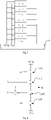
- FIG 1 is a structural diagram of a framework of an embodiment of a storage system according to the present application.
- the storage system according to the present application includes a plurality of storage chips 10.
- the storage chip 10 is an existing storage structure capable of data writing, data reading and/or data deletion.
- the storage system further includes a control chip 20.
- the storage chip 10 is stacked on the control chip 20.
- Eight storage chips 10 are schematically plotted in Figure 1 , which are stacked on the control chip 20. In other embodiments of the present application, a number of the storage chip 10 may be set according to a user requirement.
- FIG. 2 is a schematic diagram of data transmission of a storage chip and a control chip in the storage system.
- the storage chip 10 includes a data port 30, and the control chip 20 also includes a data port 40.
- the data port 30 is electrically connected to the data port 40, so that the storage chip 10 and the control chip 20 transmit data through the data port 30 and the data port 40.
- Figure 3 is a schematic structural diagram of the data port 30 arranged on the storage chip 10.
- the data port 30 arranged on the storage chip 10 includes a data output unit 31. Data of the storage chip 10 is transmitted externally through the data output unit 31, for example, to the control chip 20. Further, the data port 30 further includes a data input unit 32. External data is transmitted through the data input unit 32 to the storage chip 10.
- the data input unit 32 includes a buffer, and the external data (for example, data of the control chip 20) is inputted to the storage system through the buffer.
- the storage system further includes a serializer S, and data of the storage system, after parallel-to-serial conversion by the serializer S, is inputted to the data output unit 31 as an input signal.
- the storage system further includes a deserializer DS, and data outputted by the buffer, after serial-to-parallel conversion by the deserializer DS, is inputted to the storage system.
- Figure 4 is a schematic diagram of a circuit structure of a first embodiment of the data output unit 31.
- the data output unit 31 includes a pull-up unit 31A and a pull-down unit 31B.
- the pull-up unit 31A has a control terminal, a first terminal and a second terminal.
- a first input signal of the storage chip 10 is inputted to the control terminal, the first terminal is electrically connected to a power supply VDDQ, and the second terminal is connected to an output terminal DQ of the data output unit 31.
- the output terminal DQ is electrically connected to an external structure; for example, the output terminal DQ is electrically connected to the control chip 20 to transmit data from the storage chip 10 to the control chip 20.
- the pull-up unit is a first NMOS transistor. In the first NMOS transistor, a gate terminal is the control terminal, one of a source terminal and a drain terminal is the first terminal, and the other of the source terminal and the drain terminal is the second terminal.
- the pull-down unit 31B has a control terminal, a first terminal and a second terminal. A second input signal of the storage chip 10 is inputted to the control terminal, the first terminal is electrically connected to a ground terminal VSS, and the second terminal is connected to the output terminal DQ of the data output unit.
- the pull-down unit 31B and the pull-up unit 31A are transistors of the same type. That is, the pull-down unit 31B is a second NMOS transistor. In the second NMOS transistor, a gate terminal is the control terminal, one of a source terminal and a drain terminal is the first terminal, and the other of the source terminal and the drain terminal is the second terminal.
- the first input signal and the second input signal are complementary signals.
- the first input signal is a positive input signal Ip
- the second input signal is a negative input signal In
- they are complementary to each other, so as to output a complete signal at the output terminal DQ.
- the data output unit 31 further includes an inverter A.
- the first input signal is inputted to the control terminal of the pull-up unit 31A through the inverter A, or the second input signal is inputted to the control terminal of the pull-down unit 31B through the inverter A.
- the first input signal and the second input signal are complementary signals
- the pull-up unit 31A is an NMOS transistor
- the pull-down unit 31B is also an NMOS transistor; therefore, in order to ensure the integrity of an output signal, one of the pull-up unit 31A and the pull-down unit 31B is provided with the inverter A, so as to guarantee the integrity of the signal outputted by the output terminal DQ.
- the inverter A is arranged on a branch where the pull-down unit 31B is located; that is, the second input signal is inputted to the control terminal of the pull-down unit 31B through the inverter A.
- No inverter is arranged on a branch where the pull-up unit 31A is located; that is, the first input signal is directly inputted to the control terminal of the pull-up unit 31A.
- an inverter may be arranged on the branch where the pull-up unit 31A is located, while no inverter is arranged on the branch where the pull-down unit 31B is located.
- a voltage corresponding to a high level of an output signal of the output terminal DQ of the data output unit 31 is less than a power supply VDDQ voltage. That is, a voltage of the output terminal DQ is not required to be increased to the power supply VDDQ voltage, which reduces the time of conversion between a low level and a high level and increases a data transmission rate.
- a width of the first NMOS transistor is greater than that of the second NMOS transistor, and the first NMOS transistor and the second NMOS transistor operate in a linear region, which can further increase the data transmission rate and improve the performance of the storage system.
- the data output unit of the storage system is provided with the pull-up unit 31A and the pull-down unit 31B, wherein the pull-up unit 31A is an NMOS transistor, so that a voltage of the data output unit can be effectively accelerated from low to high or from high to low; that is, the time of conversion of the voltage of the data output unit from low to high or from high to low is reduced, thereby increasing the data transmission speed and improving the performance of the storage system.
- the pull-up unit 31A is an NMOS transistor
- FIG. 5 is a schematic circuit diagram of a first embodiment of a data output unit of the storage chip and the control chip in the storage system according to the present application.
- the data output units 31 share the power supply VDDQ and the ground terminal VSS, so as to simplify the layout and improve the space utilization.
- all the data output units 31 share the power supply VDDQ and the ground terminal VSS.
- at least some of the data output units 31 share the power supply VDDQ and the ground terminal VSS.
- the output terminal DQ of the data output unit 31 is connected to the control chip 20 through a conductive structure.
- the conductive structure may be a through-silicon-via (TSV) structure 101 as shown in FIG. 1 .
- TSV through-silicon-via
- the output terminal DQ of each data output unit 31 is connected to the control chip 20 through one TSV structure 101. That is, the output terminals DQ of the data output units 31 do not share the TSV structure 101.
- data output units 31-1, 31-2, 31-3, 31-4, 31-5, 31-6, 31-7 and 31-8 are connected to the control chip 20 through different TSV structures respectively.
- FIG. 6 is a schematic circuit diagram of a second embodiment of the data output unit of the storage chip and the control chip in the storage system according to the present application.
- the output terminals DQ of some of the data output units 31 share the same conductive structure and are electrically connected to the control chip 20.
- eight data output units 31 are schematically plotted.
- the data output units 31-1, 31-2, 31-3, 31-4 and 31-5 share the same conductive structure
- the data output units 31-6 and 31-7 share another conductive structure
- the data output unit 31-8 uses a conductive structure alone.
- Figure 7 is a schematic circuit diagram of a third embodiment of the data output unit of the storage chip and the control chip in the storage system according to the present application.
- the output terminals DQ of all the data output units 31 share the same conductive structure and are electrically connected to the control chip 20.
- the data output units 31-1, 31-2, 31-3, 31-4, 31-5, 31-6, 31-7 and 31-8 share the same conductive structure.
- switch units are added to the data output unit of the storage chip of the storage system according to the present application, so as to control ON and OFF of the data output unit 31, thereby avoiding affecting the data transmission of the storage chip 10.
- Figure 8 is a schematic diagram of a circuit structure of a second embodiment of the data output unit 31 in the storage system according to the present application.
- the data output unit 31 not only includes the pull-up unit 31A and the pull-down unit 31B, but also includes a first switch unit 31C and a second switch unit 31D.
- the first terminal of the pull-up unit 31A is electrically connected to the power supply VDDQ through the first switch unit 31C, and the first terminal of the pull-down unit 31B is electrically connected to the ground terminal VSS through the second switch unit 31D.
- the data output unit 31 can be switched between output of data and a high-impedance state (that is, no output of data) by turning on and turning off the first switch unit 31C and the second switch unit 31D.
- the data output unit 31 can output data to the control chip through the TSV structure; and when the first switch unit 31C and the second switch unit 31D are turned off, the data output unit 31 cannot output data to the control chip and presents the high-impedance state.
- the first switch unit 31C is a first transistor.
- the first transistor includes a control terminal, a first terminal and a second terminal.
- An enable signal EN is inputted to the control terminal to control ON and OFF of the first switch unit 31C.
- the first terminal is electrically connected to the power supply VDDQ.
- the second terminal is electrically connected to the first terminal of the pull-up unit 31A.
- the first transistor is a third NMOS transistor.
- a gate terminal is the control terminal, one of a source terminal and a drain terminal is the first terminal, and the other of the source terminal and the drain terminal is the second terminal.
- the first transistor may also be a PMOS transistor.
- a gate terminal is the control terminal, one of a source terminal and a drain terminal is the first terminal, and the other of the source terminal and the drain terminal is the second terminal.
- the second switch unit 31D is a second transistor.
- the second transistor includes a control terminal, a first terminal and a second terminal.
- the enable signal EN is inputted to the control terminal to control ON and OFF of the second switch unit 31D.
- the first terminal is electrically connected to the ground terminal VSS.
- the second terminal is electrically connected to the first terminal of the pull-down unit 31B.
- the second transistor is a fourth NMOS transistor.
- a gate terminal is the control terminal, one of a source terminal and a drain terminal is the first terminal, and the other of the source terminal and the drain terminal is the second terminal.
- the second transistor may also be a PMOS transistor.
- a gate terminal is the control terminal, one of the source terminal and the drain terminal is the first terminal, and the other of the source terminal and the drain terminal is the second terminal.
- the pull-up unit 31A, the pull-down unit 31B, the first switch unit 31C and the second switch unit 31D are all NMOS transistors and may share a semiconductor structure, which greatly simplifies the layout and saves a manufacturing process.
- the following illustrates how the first switch unit and the second switch unit are controlled to realize data transmission in the situation where the output terminals DQ of some of the data output units 31 share the same conductive structure and are electrically connected to the control chip 20 (as shown in Figure 6 ).
- the enable signal controls the first switch unit and the second switch unit of the data output unit 31-1 to be turned on and controls the first switch units and the second switch units of the data output units 31-2, 31-3, 31-7 and 31-8 to be turned off, so as to cut off the connection with the control chip 20 to avoid affecting the data transmission of the storage chip 10 where the data output unit 31-1 is located.
- the enable signal controls the first switch unit and the second switch unit of the data output unit 31-2 to be turned on and controls the first switch units and the second switch units of the data output units 31-1, 31-3, 31-7 and 31-8 to be turned off, so as to cut off the connection with the control chip 20 to avoid affecting the data transmission of the storage chip 10 where the data output unit 31-1 is located.
- the control over other data output units can be obtained with reference to the above description.
- the data input unit 32 is a buffer. In another embodiment of the present application, the data input unit 32 is of the same structure as the data output unit 31.
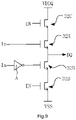
- FIG. 9 is a schematic diagram of a circuit structure of an embodiment of the data input unit 32 of the storage system according to the present application.
- the data input unit 32 includes a pull-up unit 32A, a pull-down unit 32B, a third switch unit 32C and a fourth switch unit 32D.
- the pull-up unit 32A has a control terminal, a first terminal and a second terminal.
- the first input signal of the external structure (for example, the control chip 20) is inputted to the control terminal, the first terminal is electrically connected to the power supply VDDQ through the third switch unit 32C, and the second terminal is connected to an output terminal DQ of the data input unit 32.
- the signal of the output terminal DQ is inputted to the storage chip 10.
- the pull-up unit 32A is an NMOS transistor.
- the pull-down unit 32B has a control terminal, a first terminal and a second terminal.
- the second input signal of the external structure (for example, the control chip 20) is inputted to the control terminal, the first terminal is electrically connected to the ground terminal VSS through the fourth switch unit 32D, and the second terminal is connected to the output terminal DQ of the data input unit.
- the pull-down unit 32B is an NMOS transistor. In other embodiments of the present application, the pull-down unit 32B may also be a PMOS transistor.
- the first input signal and the second input signal are complementary signals.
- the first input signal is a positive input signal Ip
- the second input signal is a negative input signal In
- they are complementary to each other, so as to output a complete signal at the output terminal DQ.
- the data input unit of the storage chip 10 of the storage system is provided with the pull-up unit 32A and the pull-down unit 32B, and the pull-up unit 32A is an NMOS transistor, so that a voltage of the data input unit can be effectively accelerated from low to high or from high to low; that is, the time of conversion of the voltage of the data input unit from low to high or from high to low is reduced, thereby greatly increasing the data transmission speed and improving the performance of the storage system.
- the data input unit 32 can be switched between input of data and a high-impedance state (that is, no input of data) by turning on and turning off the third switch unit 32C and the fourth switch unit 32D. Specifically, when the third switch unit 32C and the fourth switch unit 32D are turned on, the data input unit 32 can input data; and when the third switch unit 32C and the fourth switch unit 32D are turned off, the data input unit 32 cannot input data and presents the high-impedance state.
- the third switch unit 32C and the fourth switch unit 32D are both NMOS transistors, and then the pull-up unit 32A, the pull-down unit 32B, the third switch unit 32C and the fourth switch unit 32D can share a semiconductor structure with one another, which greatly simplifies the layout and saves the manufacturing process.
- part or all of the data input units of the storage chips may also share the same conductive structure and be electrically connected to the control chip 20.
- the connection manners thereof are the same as the data output units are not described in detail.
- the structure of the data port 30 in the storage chip 10 is described in the above embodiments. It may be understood that the data port 40 located in the control chip 20 may have the same structure as the data port 30 located in the storage chip 10. That is, the data output unit of the data port 40 located in the control chip 20 may also consist of a pull-up unit and a pull-down unit, thereby greatly increasing a rate at which data is transmitted from the control chip 20 to the storage chip 10 or other structural layers.
- the data input unit of the data port 40 located in the control chip 20 may also consist of a pull-up unit and a pull-down unit, thereby greatly increasing a rate at which data is transmitted from the external structure (such as the storage chip or other structural layers) to the control chip 20.
Landscapes
- Engineering & Computer Science (AREA)
- Theoretical Computer Science (AREA)
- General Engineering & Computer Science (AREA)
- Physics & Mathematics (AREA)
- General Physics & Mathematics (AREA)
- Computer Hardware Design (AREA)
- Mathematical Physics (AREA)
- Computing Systems (AREA)
- Power Engineering (AREA)
- Microelectronics & Electronic Packaging (AREA)
- Dram (AREA)
- Logic Circuits (AREA)
- Semiconductor Integrated Circuits (AREA)
Applications Claiming Priority (2)
| Application Number | Priority Date | Filing Date | Title |
|---|---|---|---|
| CN202010766270.9A CN114067860B (zh) | 2020-08-03 | 2020-08-03 | 存储系统 |
| PCT/CN2021/075455 WO2022027947A1 (zh) | 2020-08-03 | 2021-02-05 | 存储系统 |
Publications (2)
| Publication Number | Publication Date |
|---|---|
| EP4033489A1 true EP4033489A1 (de) | 2022-07-27 |
| EP4033489A4 EP4033489A4 (de) | 2023-08-23 |
Family
ID=80116933
Family Applications (1)
| Application Number | Title | Priority Date | Filing Date |
|---|---|---|---|
| EP21853076.4A Ceased EP4033489A4 (de) | 2020-08-03 | 2021-02-05 | Speichersystem |
Country Status (4)
| Country | Link |
|---|---|
| US (1) | US20220129397A1 (de) |
| EP (1) | EP4033489A4 (de) |
| CN (1) | CN114067860B (de) |
| WO (1) | WO2022027947A1 (de) |
Family Cites Families (22)
| Publication number | Priority date | Publication date | Assignee | Title |
|---|---|---|---|---|
| KR100238247B1 (ko) * | 1997-05-16 | 2000-01-15 | 윤종용 | 고속 저전력 신호라인 드라이버 및 이를 이용한 반도체메모리장치 |
| KR100422821B1 (ko) * | 1997-06-30 | 2004-05-24 | 주식회사 하이닉스반도체 | 출력 버퍼 장치 |
| DE19856690A1 (de) * | 1997-12-30 | 1999-07-01 | Samsung Electronics Co Ltd | Ausgangstreiberschaltung und eine solche enthaltendes integriertes Speicherschaltkreisbauelement |
| JP3808623B2 (ja) * | 1998-04-27 | 2006-08-16 | 株式会社東芝 | データ入出力回路、半導体記憶装置および情報処理装置 |
| JP2002367376A (ja) * | 2001-06-12 | 2002-12-20 | Mitsubishi Electric Corp | 半導体装置 |
| US7453725B2 (en) * | 2006-10-06 | 2008-11-18 | Atmel Corporation | Apparatus for eliminating leakage current of a low Vt device in a column latch |
| KR101044507B1 (ko) * | 2009-06-29 | 2011-06-27 | 주식회사 하이닉스반도체 | 메모리 칩 패키지 장치 |
| US8120968B2 (en) * | 2010-02-12 | 2012-02-21 | International Business Machines Corporation | High voltage word line driver |
| KR20130045144A (ko) * | 2011-10-24 | 2013-05-03 | 삼성전자주식회사 | 출력 드라이버와 이를 포함하는 장치들, 및 접지 터미네이션 |
| CN103066987A (zh) * | 2011-10-24 | 2013-04-24 | 三星电子株式会社 | 输出驱动器、集成电路及系统 |
| KR101989571B1 (ko) * | 2012-06-27 | 2019-06-14 | 삼성전자주식회사 | 고전압 및 와이드 랜지 전압 동작을 위한 출력 드라이버 및 그것을 사용한 데이터 출력 드라이빙 회로 |
| CN103744803B (zh) * | 2014-01-26 | 2017-08-25 | 无锡云动科技发展有限公司 | 一种电源组件及存储系统 |
| KR20150109209A (ko) * | 2014-03-19 | 2015-10-01 | 에스케이하이닉스 주식회사 | 반도체 장치 |
| US9799393B1 (en) * | 2016-05-31 | 2017-10-24 | Globalfoundries Inc. | Methods, apparatus and system for providing NMOS-only memory cells |
| KR102799068B1 (ko) * | 2017-02-09 | 2025-04-23 | 에스케이하이닉스 주식회사 | 저장 장치 및 그 동작 방법 |
| KR102672957B1 (ko) * | 2017-02-13 | 2024-06-10 | 에스케이하이닉스 주식회사 | 데이터 출력 버퍼 |
| US10490238B2 (en) * | 2017-06-29 | 2019-11-26 | SK Hynix Inc. | Serializer and memory device including the same |
| US10347325B1 (en) * | 2018-06-29 | 2019-07-09 | Realtek Semiconductor Corporation | DDR4 memory I/O driver |
| CN109346117A (zh) * | 2018-11-15 | 2019-02-15 | 珠海天威技术开发有限公司 | Eeprom存储电路、eeprom存储芯片、耗材容器以及成像设备 |
| KR102708728B1 (ko) * | 2019-01-15 | 2024-09-23 | 에스케이하이닉스 주식회사 | 반도체장치 및 반도체시스템 |
| US10902907B1 (en) * | 2019-10-02 | 2021-01-26 | Micron Technology, Inc. | Output drivers, and related methods, memory devices, and systems |
| CN210606642U (zh) * | 2019-10-16 | 2020-05-22 | 长鑫存储技术有限公司 | 输出驱动电路及存储器 |
-
2020
- 2020-08-03 CN CN202010766270.9A patent/CN114067860B/zh active Active
-
2021
- 2021-02-05 EP EP21853076.4A patent/EP4033489A4/de not_active Ceased
- 2021-02-05 WO PCT/CN2021/075455 patent/WO2022027947A1/zh not_active Ceased
-
2022
- 2022-01-11 US US17/647,650 patent/US20220129397A1/en not_active Abandoned
Also Published As
| Publication number | Publication date |
|---|---|
| WO2022027947A1 (zh) | 2022-02-10 |
| EP4033489A4 (de) | 2023-08-23 |
| CN114067860B (zh) | 2024-03-26 |
| CN114067860A (zh) | 2022-02-18 |
| US20220129397A1 (en) | 2022-04-28 |
Similar Documents
| Publication | Publication Date | Title |
|---|---|---|
| US7013359B1 (en) | High speed memory interface system and method | |
| CN113223577B (zh) | 用于降低动态功率和峰值电流的sram位线和写入辅助装置与方法及双输入电平移位器 | |
| US20120324152A1 (en) | Memory controller with bi-directional buffer for achieving high speed capability and related method thereof | |
| US6750680B2 (en) | Semiconductor integrated circuit, logic operation circuit, and flip flop | |
| US9318420B2 (en) | Chip stack packages, system in packages including the same, and methods of operating the same | |
| US20050024243A1 (en) | Serializer and method of serializing parallel data into serial data stream | |
| US9153533B2 (en) | Microelectronic elements with master/slave configurability | |
| US20030208668A1 (en) | Single-ended memory interface system | |
| US6378008B1 (en) | Output data path scheme in a memory device | |
| US20040100947A1 (en) | Multiplexer circuit for converting parallel data into serial data at high speed and synchronizing the serial data with a clock signal | |
| US9859892B2 (en) | Semiconductor apparatus reducing a parasitic capacitance | |
| CN102857206A (zh) | 接收电路 | |
| EP4033489A1 (de) | Speichersystem | |
| US11798635B2 (en) | Semiconductor integrated circuit | |
| CN101261989A (zh) | 集成电路 | |
| US11823765B2 (en) | Storage system | |
| US4918329A (en) | Data transmission system | |
| US4819208A (en) | Biodirectional elastic store circuit | |
| US20240005965A1 (en) | Circuit for receiving data, system for receiving data, and memory device | |
| US4110697A (en) | Digital bypassable register interface | |
| US7579876B1 (en) | Multi-use input/output pin systems and methods | |
| US20250069646A1 (en) | Control circuit, control method, and memory | |
| US11888474B2 (en) | On die termination circuit and memory device | |
| US20250069645A1 (en) | Control circuit, control method, and memory | |
| US20230170013A1 (en) | Apparatuses including output drivers and methods for providing output data signals |
Legal Events
| Date | Code | Title | Description |
|---|---|---|---|
| STAA | Information on the status of an ep patent application or granted ep patent |
Free format text: STATUS: THE INTERNATIONAL PUBLICATION HAS BEEN MADE |
|
| PUAI | Public reference made under article 153(3) epc to a published international application that has entered the european phase |
Free format text: ORIGINAL CODE: 0009012 |
|
| STAA | Information on the status of an ep patent application or granted ep patent |
Free format text: STATUS: REQUEST FOR EXAMINATION WAS MADE |
|
| 17P | Request for examination filed |
Effective date: 20220422 |
|
| AK | Designated contracting states |
Kind code of ref document: A1 Designated state(s): AL AT BE BG CH CY CZ DE DK EE ES FI FR GB GR HR HU IE IS IT LI LT LU LV MC MK MT NL NO PL PT RO RS SE SI SK SM TR |
|
| RIC1 | Information provided on ipc code assigned before grant |
Ipc: G06F 13/40 20060101ALI20230309BHEP Ipc: G06F 13/42 20060101ALI20230309BHEP Ipc: H03K 19/017 20060101ALI20230309BHEP Ipc: H03K 19/17784 20200101ALI20230309BHEP Ipc: G11C 16/02 20060101ALI20230309BHEP Ipc: G11C 11/4076 20060101ALI20230309BHEP Ipc: G11C 7/10 20060101AFI20230309BHEP |
|
| A4 | Supplementary search report drawn up and despatched |
Effective date: 20230725 |
|
| RIC1 | Information provided on ipc code assigned before grant |
Ipc: G06F 13/40 20060101ALI20230719BHEP Ipc: G06F 13/42 20060101ALI20230719BHEP Ipc: H03K 19/017 20060101ALI20230719BHEP Ipc: H03K 19/17784 20200101ALI20230719BHEP Ipc: G11C 16/02 20060101ALI20230719BHEP Ipc: G11C 11/4076 20060101ALI20230719BHEP Ipc: G11C 7/10 20060101AFI20230719BHEP |
|
| DAV | Request for validation of the european patent (deleted) | ||
| DAX | Request for extension of the european patent (deleted) | ||
| STAA | Information on the status of an ep patent application or granted ep patent |
Free format text: STATUS: EXAMINATION IS IN PROGRESS |
|
| 17Q | First examination report despatched |
Effective date: 20240301 |
|
| REG | Reference to a national code |
Ref country code: DE Ref legal event code: R003 |
|
| STAA | Information on the status of an ep patent application or granted ep patent |
Free format text: STATUS: THE APPLICATION HAS BEEN REFUSED |
|
| 18R | Application refused |
Effective date: 20250204 |