EP4030467B1 - Verfahren zum direkten hydrophilen bonden von substraten - Google Patents
Verfahren zum direkten hydrophilen bonden von substraten Download PDFInfo
- Publication number
- EP4030467B1 EP4030467B1 EP22151346.8A EP22151346A EP4030467B1 EP 4030467 B1 EP4030467 B1 EP 4030467B1 EP 22151346 A EP22151346 A EP 22151346A EP 4030467 B1 EP4030467 B1 EP 4030467B1
- Authority
- EP
- European Patent Office
- Prior art keywords
- layer
- substrate
- bonding
- semiconductor material
- bonding layer
- Prior art date
- Legal status (The legal status is an assumption and is not a legal conclusion. Google has not performed a legal analysis and makes no representation as to the accuracy of the status listed.)
- Active
Links
- 239000000758 substrate Substances 0.000 title claims description 169
- 238000000034 method Methods 0.000 title claims description 49
- 239000000463 material Substances 0.000 claims description 74
- 239000004065 semiconductor Substances 0.000 claims description 71
- 238000010438 heat treatment Methods 0.000 claims description 35
- 238000002425 crystallisation Methods 0.000 claims description 28
- 238000000151 deposition Methods 0.000 claims description 24
- 239000003989 dielectric material Substances 0.000 claims description 18
- 230000008021 deposition Effects 0.000 claims description 17
- 230000015572 biosynthetic process Effects 0.000 claims description 15
- XLYOFNOQVPJJNP-UHFFFAOYSA-N water Substances O XLYOFNOQVPJJNP-UHFFFAOYSA-N 0.000 claims description 14
- 238000002513 implantation Methods 0.000 claims description 13
- 238000005224 laser annealing Methods 0.000 claims description 11
- 238000011282 treatment Methods 0.000 claims description 8
- 229910052698 phosphorus Inorganic materials 0.000 claims description 6
- 238000005280 amorphization Methods 0.000 claims description 5
- 238000012546 transfer Methods 0.000 claims description 4
- 229910052757 nitrogen Inorganic materials 0.000 claims description 3
- 239000010410 layer Substances 0.000 description 250
- XUIMIQQOPSSXEZ-UHFFFAOYSA-N Silicon Chemical compound [Si] XUIMIQQOPSSXEZ-UHFFFAOYSA-N 0.000 description 26
- 230000008025 crystallization Effects 0.000 description 26
- 229910052710 silicon Inorganic materials 0.000 description 18
- 239000010703 silicon Substances 0.000 description 17
- 229910021417 amorphous silicon Inorganic materials 0.000 description 13
- 230000008569 process Effects 0.000 description 13
- 238000004377 microelectronic Methods 0.000 description 12
- 239000002019 doping agent Substances 0.000 description 11
- UFHFLCQGNIYNRP-UHFFFAOYSA-N Hydrogen Chemical compound [H][H] UFHFLCQGNIYNRP-UHFFFAOYSA-N 0.000 description 8
- VYPSYNLAJGMNEJ-UHFFFAOYSA-N Silicium dioxide Chemical compound O=[Si]=O VYPSYNLAJGMNEJ-UHFFFAOYSA-N 0.000 description 8
- 238000000137 annealing Methods 0.000 description 8
- 229910052732 germanium Inorganic materials 0.000 description 8
- 230000010354 integration Effects 0.000 description 8
- GNPVGFCGXDBREM-UHFFFAOYSA-N germanium atom Chemical compound [Ge] GNPVGFCGXDBREM-UHFFFAOYSA-N 0.000 description 7
- 238000004519 manufacturing process Methods 0.000 description 7
- 238000005498 polishing Methods 0.000 description 7
- 238000006243 chemical reaction Methods 0.000 description 6
- 229910052814 silicon oxide Inorganic materials 0.000 description 6
- LEVVHYCKPQWKOP-UHFFFAOYSA-N [Si].[Ge] Chemical compound [Si].[Ge] LEVVHYCKPQWKOP-UHFFFAOYSA-N 0.000 description 5
- 239000012212 insulator Substances 0.000 description 5
- 238000007254 oxidation reaction Methods 0.000 description 5
- 238000000623 plasma-assisted chemical vapour deposition Methods 0.000 description 5
- 239000000126 substance Substances 0.000 description 5
- 238000000231 atomic layer deposition Methods 0.000 description 4
- 230000007547 defect Effects 0.000 description 4
- 238000009792 diffusion process Methods 0.000 description 4
- 238000004518 low pressure chemical vapour deposition Methods 0.000 description 4
- 230000003647 oxidation Effects 0.000 description 4
- 229910000577 Silicon-germanium Inorganic materials 0.000 description 3
- 229910052785 arsenic Inorganic materials 0.000 description 3
- 230000008901 benefit Effects 0.000 description 3
- 238000005229 chemical vapour deposition Methods 0.000 description 3
- 238000005530 etching Methods 0.000 description 3
- 238000005468 ion implantation Methods 0.000 description 3
- 229910021420 polycrystalline silicon Inorganic materials 0.000 description 3
- 229920000642 polymer Polymers 0.000 description 3
- 239000002243 precursor Substances 0.000 description 3
- HBMJWWWQQXIZIP-UHFFFAOYSA-N silicon carbide Chemical compound [Si+]#[C-] HBMJWWWQQXIZIP-UHFFFAOYSA-N 0.000 description 3
- 229910010271 silicon carbide Inorganic materials 0.000 description 3
- 241000894007 species Species 0.000 description 3
- ZOXJGFHDIHLPTG-UHFFFAOYSA-N Boron Chemical compound [B] ZOXJGFHDIHLPTG-UHFFFAOYSA-N 0.000 description 2
- RYGMFSIKBFXOCR-UHFFFAOYSA-N Copper Chemical compound [Cu] RYGMFSIKBFXOCR-UHFFFAOYSA-N 0.000 description 2
- GYHNNYVSQQEPJS-UHFFFAOYSA-N Gallium Chemical compound [Ga] GYHNNYVSQQEPJS-UHFFFAOYSA-N 0.000 description 2
- OAICVXFJPJFONN-UHFFFAOYSA-N Phosphorus Chemical compound [P] OAICVXFJPJFONN-UHFFFAOYSA-N 0.000 description 2
- BLRPTPMANUNPDV-UHFFFAOYSA-N Silane Chemical compound [SiH4] BLRPTPMANUNPDV-UHFFFAOYSA-N 0.000 description 2
- 239000000370 acceptor Substances 0.000 description 2
- 230000004913 activation Effects 0.000 description 2
- RQNWIZPPADIBDY-UHFFFAOYSA-N arsenic atom Chemical compound [As] RQNWIZPPADIBDY-UHFFFAOYSA-N 0.000 description 2
- 230000004888 barrier function Effects 0.000 description 2
- 229910052796 boron Inorganic materials 0.000 description 2
- 239000003795 chemical substances by application Substances 0.000 description 2
- 230000006835 compression Effects 0.000 description 2
- 238000007906 compression Methods 0.000 description 2
- 229910052802 copper Inorganic materials 0.000 description 2
- 239000010949 copper Substances 0.000 description 2
- PZPGRFITIJYNEJ-UHFFFAOYSA-N disilane Chemical compound [SiH3][SiH3] PZPGRFITIJYNEJ-UHFFFAOYSA-N 0.000 description 2
- 238000010292 electrical insulation Methods 0.000 description 2
- 239000012777 electrically insulating material Substances 0.000 description 2
- 238000000407 epitaxy Methods 0.000 description 2
- 229910052733 gallium Inorganic materials 0.000 description 2
- 229910052739 hydrogen Inorganic materials 0.000 description 2
- 239000001257 hydrogen Substances 0.000 description 2
- 239000012535 impurity Substances 0.000 description 2
- 238000001659 ion-beam spectroscopy Methods 0.000 description 2
- 238000001451 molecular beam epitaxy Methods 0.000 description 2
- 230000005693 optoelectronics Effects 0.000 description 2
- 239000011574 phosphorus Substances 0.000 description 2
- 238000005240 physical vapour deposition Methods 0.000 description 2
- 238000004151 rapid thermal annealing Methods 0.000 description 2
- 238000001953 recrystallisation Methods 0.000 description 2
- 238000012552 review Methods 0.000 description 2
- 239000007790 solid phase Substances 0.000 description 2
- 238000012360 testing method Methods 0.000 description 2
- 239000010409 thin film Substances 0.000 description 2
- WFKWXMTUELFFGS-UHFFFAOYSA-N tungsten Chemical compound [W] WFKWXMTUELFFGS-UHFFFAOYSA-N 0.000 description 2
- 229910052721 tungsten Inorganic materials 0.000 description 2
- 239000010937 tungsten Substances 0.000 description 2
- OKTJSMMVPCPJKN-UHFFFAOYSA-N Carbon Chemical compound [C] OKTJSMMVPCPJKN-UHFFFAOYSA-N 0.000 description 1
- CURLTUGMZLYLDI-UHFFFAOYSA-N Carbon dioxide Chemical compound O=C=O CURLTUGMZLYLDI-UHFFFAOYSA-N 0.000 description 1
- WHXSMMKQMYFTQS-UHFFFAOYSA-N Lithium Chemical compound [Li] WHXSMMKQMYFTQS-UHFFFAOYSA-N 0.000 description 1
- 229910007264 Si2H6 Inorganic materials 0.000 description 1
- 229910052581 Si3N4 Inorganic materials 0.000 description 1
- 241001080024 Telles Species 0.000 description 1
- 230000003213 activating effect Effects 0.000 description 1
- 239000012790 adhesive layer Substances 0.000 description 1
- 229910052782 aluminium Inorganic materials 0.000 description 1
- XAGFODPZIPBFFR-UHFFFAOYSA-N aluminium Chemical compound [Al] XAGFODPZIPBFFR-UHFFFAOYSA-N 0.000 description 1
- 229910052787 antimony Inorganic materials 0.000 description 1
- WATWJIUSRGPENY-UHFFFAOYSA-N antimony atom Chemical compound [Sb] WATWJIUSRGPENY-UHFFFAOYSA-N 0.000 description 1
- 229910052797 bismuth Inorganic materials 0.000 description 1
- JCXGWMGPZLAOME-UHFFFAOYSA-N bismuth atom Chemical compound [Bi] JCXGWMGPZLAOME-UHFFFAOYSA-N 0.000 description 1
- 229910052799 carbon Inorganic materials 0.000 description 1
- 229910002090 carbon oxide Inorganic materials 0.000 description 1
- 238000003486 chemical etching Methods 0.000 description 1
- 238000004140 cleaning Methods 0.000 description 1
- 229910052681 coesite Inorganic materials 0.000 description 1
- 230000000295 complement effect Effects 0.000 description 1
- 239000002131 composite material Substances 0.000 description 1
- 229910052906 cristobalite Inorganic materials 0.000 description 1
- 238000011161 development Methods 0.000 description 1
- 229910003460 diamond Inorganic materials 0.000 description 1
- 239000010432 diamond Substances 0.000 description 1
- 238000010894 electron beam technology Methods 0.000 description 1
- 230000008030 elimination Effects 0.000 description 1
- 238000003379 elimination reaction Methods 0.000 description 1
- 239000002360 explosive Substances 0.000 description 1
- 239000010408 film Substances 0.000 description 1
- 239000007789 gas Substances 0.000 description 1
- 229910021478 group 5 element Inorganic materials 0.000 description 1
- XLYOFNOQVPJJNP-ZSJDYOACSA-N heavy water Substances [2H]O[2H] XLYOFNOQVPJJNP-ZSJDYOACSA-N 0.000 description 1
- 239000001307 helium Substances 0.000 description 1
- 229910052734 helium Inorganic materials 0.000 description 1
- SWQJXJOGLNCZEY-UHFFFAOYSA-N helium atom Chemical compound [He] SWQJXJOGLNCZEY-UHFFFAOYSA-N 0.000 description 1
- 230000002209 hydrophobic effect Effects 0.000 description 1
- 229910052738 indium Inorganic materials 0.000 description 1
- APFVFJFRJDLVQX-UHFFFAOYSA-N indium atom Chemical compound [In] APFVFJFRJDLVQX-UHFFFAOYSA-N 0.000 description 1
- 238000009413 insulation Methods 0.000 description 1
- 239000012705 liquid precursor Substances 0.000 description 1
- 229910052744 lithium Inorganic materials 0.000 description 1
- 238000005259 measurement Methods 0.000 description 1
- 230000008018 melting Effects 0.000 description 1
- 238000002844 melting Methods 0.000 description 1
- 229910052751 metal Inorganic materials 0.000 description 1
- 239000002184 metal Substances 0.000 description 1
- 239000007769 metal material Substances 0.000 description 1
- 230000001590 oxidative effect Effects 0.000 description 1
- 238000009832 plasma treatment Methods 0.000 description 1
- 229920005591 polysilicon Polymers 0.000 description 1
- 238000012545 processing Methods 0.000 description 1
- 230000001737 promoting effect Effects 0.000 description 1
- 229910000077 silane Inorganic materials 0.000 description 1
- 239000000377 silicon dioxide Substances 0.000 description 1
- 235000012239 silicon dioxide Nutrition 0.000 description 1
- HQVNEWCFYHHQES-UHFFFAOYSA-N silicon nitride Chemical compound N12[Si]34N5[Si]62N3[Si]51N64 HQVNEWCFYHHQES-UHFFFAOYSA-N 0.000 description 1
- 239000002210 silicon-based material Substances 0.000 description 1
- 229910052682 stishovite Inorganic materials 0.000 description 1
- 238000000427 thin-film deposition Methods 0.000 description 1
- 230000009466 transformation Effects 0.000 description 1
- 230000001131 transforming effect Effects 0.000 description 1
- 229910052905 tridymite Inorganic materials 0.000 description 1
- 239000012808 vapor phase Substances 0.000 description 1
Images


Classifications
-
- H—ELECTRICITY
- H01—ELECTRIC ELEMENTS
- H01L—SEMICONDUCTOR DEVICES NOT COVERED BY CLASS H10
- H01L21/00—Processes or apparatus adapted for the manufacture or treatment of semiconductor or solid state devices or of parts thereof
- H01L21/70—Manufacture or treatment of devices consisting of a plurality of solid state components formed in or on a common substrate or of parts thereof; Manufacture of integrated circuit devices or of parts thereof
- H01L21/71—Manufacture of specific parts of devices defined in group H01L21/70
- H01L21/76—Making of isolation regions between components
- H01L21/762—Dielectric regions, e.g. EPIC dielectric isolation, LOCOS; Trench refilling techniques, SOI technology, use of channel stoppers
- H01L21/7624—Dielectric regions, e.g. EPIC dielectric isolation, LOCOS; Trench refilling techniques, SOI technology, use of channel stoppers using semiconductor on insulator [SOI] technology
- H01L21/76251—Dielectric regions, e.g. EPIC dielectric isolation, LOCOS; Trench refilling techniques, SOI technology, use of channel stoppers using semiconductor on insulator [SOI] technology using bonding techniques
-
- H—ELECTRICITY
- H01—ELECTRIC ELEMENTS
- H01L—SEMICONDUCTOR DEVICES NOT COVERED BY CLASS H10
- H01L21/00—Processes or apparatus adapted for the manufacture or treatment of semiconductor or solid state devices or of parts thereof
- H01L21/02—Manufacture or treatment of semiconductor devices or of parts thereof
- H01L21/04—Manufacture or treatment of semiconductor devices or of parts thereof the devices having potential barriers, e.g. a PN junction, depletion layer or carrier concentration layer
- H01L21/18—Manufacture or treatment of semiconductor devices or of parts thereof the devices having potential barriers, e.g. a PN junction, depletion layer or carrier concentration layer the devices having semiconductor bodies comprising elements of Group IV of the Periodic Table or AIIIBV compounds with or without impurities, e.g. doping materials
- H01L21/185—Joining of semiconductor bodies for junction formation
- H01L21/187—Joining of semiconductor bodies for junction formation by direct bonding
-
- H—ELECTRICITY
- H01—ELECTRIC ELEMENTS
- H01L—SEMICONDUCTOR DEVICES NOT COVERED BY CLASS H10
- H01L21/00—Processes or apparatus adapted for the manufacture or treatment of semiconductor or solid state devices or of parts thereof
- H01L21/02—Manufacture or treatment of semiconductor devices or of parts thereof
- H01L21/02002—Preparing wafers
-
- H—ELECTRICITY
- H01—ELECTRIC ELEMENTS
- H01L—SEMICONDUCTOR DEVICES NOT COVERED BY CLASS H10
- H01L21/00—Processes or apparatus adapted for the manufacture or treatment of semiconductor or solid state devices or of parts thereof
- H01L21/70—Manufacture or treatment of devices consisting of a plurality of solid state components formed in or on a common substrate or of parts thereof; Manufacture of integrated circuit devices or of parts thereof
- H01L21/71—Manufacture of specific parts of devices defined in group H01L21/70
- H01L21/76—Making of isolation regions between components
- H01L21/762—Dielectric regions, e.g. EPIC dielectric isolation, LOCOS; Trench refilling techniques, SOI technology, use of channel stoppers
- H01L21/7624—Dielectric regions, e.g. EPIC dielectric isolation, LOCOS; Trench refilling techniques, SOI technology, use of channel stoppers using semiconductor on insulator [SOI] technology
- H01L21/76251—Dielectric regions, e.g. EPIC dielectric isolation, LOCOS; Trench refilling techniques, SOI technology, use of channel stoppers using semiconductor on insulator [SOI] technology using bonding techniques
- H01L21/76254—Dielectric regions, e.g. EPIC dielectric isolation, LOCOS; Trench refilling techniques, SOI technology, use of channel stoppers using semiconductor on insulator [SOI] technology using bonding techniques with separation/delamination along an ion implanted layer, e.g. Smart-cut, Unibond
-
- H—ELECTRICITY
- H01—ELECTRIC ELEMENTS
- H01L—SEMICONDUCTOR DEVICES NOT COVERED BY CLASS H10
- H01L21/00—Processes or apparatus adapted for the manufacture or treatment of semiconductor or solid state devices or of parts thereof
- H01L21/70—Manufacture or treatment of devices consisting of a plurality of solid state components formed in or on a common substrate or of parts thereof; Manufacture of integrated circuit devices or of parts thereof
- H01L21/71—Manufacture of specific parts of devices defined in group H01L21/70
- H01L21/76—Making of isolation regions between components
- H01L21/763—Polycrystalline semiconductor regions
-
- H—ELECTRICITY
- H01—ELECTRIC ELEMENTS
- H01L—SEMICONDUCTOR DEVICES NOT COVERED BY CLASS H10
- H01L21/00—Processes or apparatus adapted for the manufacture or treatment of semiconductor or solid state devices or of parts thereof
- H01L21/02—Manufacture or treatment of semiconductor devices or of parts thereof
- H01L21/04—Manufacture or treatment of semiconductor devices or of parts thereof the devices having potential barriers, e.g. a PN junction, depletion layer or carrier concentration layer
- H01L21/18—Manufacture or treatment of semiconductor devices or of parts thereof the devices having potential barriers, e.g. a PN junction, depletion layer or carrier concentration layer the devices having semiconductor bodies comprising elements of Group IV of the Periodic Table or AIIIBV compounds with or without impurities, e.g. doping materials
- H01L21/26—Bombardment with radiation
- H01L21/263—Bombardment with radiation with high-energy radiation
- H01L21/265—Bombardment with radiation with high-energy radiation producing ion implantation
-
- H—ELECTRICITY
- H01—ELECTRIC ELEMENTS
- H01L—SEMICONDUCTOR DEVICES NOT COVERED BY CLASS H10
- H01L21/00—Processes or apparatus adapted for the manufacture or treatment of semiconductor or solid state devices or of parts thereof
- H01L21/02—Manufacture or treatment of semiconductor devices or of parts thereof
- H01L21/04—Manufacture or treatment of semiconductor devices or of parts thereof the devices having potential barriers, e.g. a PN junction, depletion layer or carrier concentration layer
- H01L21/18—Manufacture or treatment of semiconductor devices or of parts thereof the devices having potential barriers, e.g. a PN junction, depletion layer or carrier concentration layer the devices having semiconductor bodies comprising elements of Group IV of the Periodic Table or AIIIBV compounds with or without impurities, e.g. doping materials
- H01L21/26—Bombardment with radiation
- H01L21/263—Bombardment with radiation with high-energy radiation
- H01L21/268—Bombardment with radiation with high-energy radiation using electromagnetic radiation, e.g. laser radiation
Definitions
- the invention relates to a process for direct hydrophilic bonding of substrates for applications in microelectronics, optoelectronics or optics. It finds for particularly advantageous application the monolithic integration in 3D of microelectronic components.
- substrates in particular semiconductor substrates, in order to form structures suitable for the manufacture of devices for microelectronics, optoelectronics or optics.
- structures of the semiconductor-on-insulator type successively comprise a support substrate, an electrically insulating layer and a thin semiconductor layer, called the active layer.
- the active layer is made of silicon
- the structure is called “silicon on insulator” (or SOI, acronym for the Anglo-Saxon term “Silicon On Insulator”).
- SOI silicon on insulator
- SOI silicon on Insulator
- the electrically insulating layer is generally a layer of silicon oxide and is often called “buried oxide layer” (or BOX, acronym for the Anglo-Saxon term Buried OXide).
- the bonding is a direct bonding, that is to say without an adhesive layer applied.
- This bonding is advantageously of the hydrophilic type, that is to say that the adhesion between the donor substrate and the support substrate takes place via water molecules present at the bonding interface. The water is removed later by the implementation of a heat treatment.
- this bonding is carried out at ambient pressure.
- the surfaces in contact of the support substrate and of the donor substrate must have a very low roughness, typically of the order of 1 to a few nm RMS. Despite this, due to the high rigidity and hardness of the substrates, their contacting will always take place on a few asperities.
- the asperities present on the surface of the substrates generate cavities at the interface between the two substrates; the bonding interface is therefore not completely closed.
- the contact surface increases, due to the atomic mobility at the interface, until the asperities are crushed, which leads to the elimination of the cavities; the paste interface is then closed.
- the temperature to be applied is typically 1200° C. for several hours.
- the temperature to be applied is typically 1100° C. for 2 hours; this temperature can be reduced to 1050° C. for 2 hours when a plasma treatment is applied beforehand to the oxide layer.
- Such high temperature heat treatments are generally very expensive. They must be made with slow temperature rises so as not to risk deforming the substrates, which causes long processing times, or else under extremely controlled heating conditions, which requires complex equipment. Furthermore, semiconductor materials can be damaged at high temperatures.
- an interface closure defect can be extremely damaging to the integrity and performance of the bonded structure.
- a first consequence of an imperfect closing of the interface is a localized detachment, in particular on the edges of the bonded structure.
- the disbonded areas on the edge of the plates are redeposited locally on the surface of the substrate, creating areas unsuitable for the subsequent fabrication of devices electronics. These defects are called "flakes" according to the Anglo-Saxon terminology.
- a second consequence of an imperfect closing of the interface is that the cavities present at the level of the interface are zones likely to be attacked in a privileged manner by a chemical etching agent.
- the etching agent can indeed be inserted into the interface through these cavities and preferentially etch the materials present at the interface.
- metallic layers for example copper, tungsten
- the bonding interface or else of polymer deposits makes it possible to achieve low interface closing temperatures, typically less than 500°C.
- metallic materials being electrically conductive or generators of impurities in semiconductor substrates, are incompatible with a large number of microelectronic applications.
- the polymers are unstable at the manufacturing temperatures of the circuits.
- documents US2003129780A1 , US2006264004A1 And US2003141502 A1 describe a method of forming an SOI structure comprising an amorphous layer doped at the bonding interface.
- An object of the present invention is therefore to provide a process for the direct hydrophilic bonding of two substrates in which the bonding interface is closed by means of a heat treatment at a lower temperature than in the existing processes.
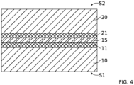
- Another object of the present invention is to provide a method of manufacturing a structure as shown in the figure 4 in which the bonding interface is closed by means of a heat treatment at a lower temperature than in the existing methods and/or in which the mechanical-chemical polishing of the surfaces to be bonded together is not necessary.
- the process according to the invention makes it possible to manufacture, at low temperature, and more particularly at a temperature less than or equal to 900° C., or even less than or equal to 600° C., a composite structure comprising a buried electrically conductive layer, such as in the case of the structure shown in the figure 4 and discussed in the introduction. More particularly, the fact that the bonding layer is doped and is present at the bonding interface activates the plasticity of the bonding surface that it constitutes and allows interface closure at a lower temperature than without doping; the presence of the oxide layer at less than 20 nm from the bonding interface will make it possible to manage the water present at the bonding interface allowing the closure of the bonding interface.
- the oxide layer When the oxide layer is located under the bonding layer, the latter is preferably less than 20 nm thick.
- the bonding layer may be located only on one of the first major surface and the second major surface and the oxide layer may be located on the other of the first major surface and the second major surface.
- the thickness of the bonding layer is not preferably limited to 20 nm, but may for example have a thickness of between 20 and 50 nm.
- Another aspect relates to a device obtained by the method introduced above.
- the bonding layer has a thickness substantially between 1 and 50 nm, more particularly between 3 and 10 nm.
- the heat treatment is carried out at a temperature substantially less than or equal to 900°C, preferably substantially less than or equal to 600°C.
- the formation of the bonding layer of an amorphous semiconductor material comprising doping elements comprises a step of depositing said amorphous semiconductor material on said main surface of the corresponding substrate, the doping elements being introduced into the layer of bonding during the deposition of the amorphous semiconductor material or after this deposition by implantation.
- the first substrate and the second substrate each comprise a layer of a monocrystalline semiconductor material, at least one of the first and second substrates comprising a layer of a dielectric material placed on the layer of a semiconductor material monocrystalline, the first and/or the second main surface being formed by the free face of the layer made of a dielectric material.
- the oxide layer can be constituted by, or be included in, the layer of a dielectric material.
- the content of the bonding layer in doping elements is parameterized, at least in terms of nature and concentration of the doping elements, so that the crystallization step generates an electrically conductive polycrystalline layer.
- the doping element(s) are preferably chosen from phosphorus, boron, arsenic, gallium, etc.
- the introduction of the doping elements of the bonding layer can be carried out by ion implantation of the (of) doping element(s) in a layer based on a semiconductor material previously formed on said main surface of the corresponding substrate; alternatively, the doping of the bonding layer can be carried out by depositing a layer of a semiconductor material on said main surface of the corresponding substrate in the presence of a gas or plasma comprising the doping element(s) (s).
- the first substrate and the second substrate each comprise a layer of a semiconductor material and a layer of a dielectric material and the bringing into contact of the first and second substrates is such that the layer of a dielectric material of each substrate electrically insulates the layer made of a semiconductor material from the substrate and the bonding interface closed by the application of the heat treatment. It is thus possible to manufacture a structure such as that illustrated in the figure 4 .
- the layer of dielectric material of at least one of the first and second substrates, or even of each substrate can be formed by thermal oxidation of a thickness of the substrate.
- At least one of the layers in a dielectric material of the first substrate and of the second substrate, preferably one of the two, can constitute, or comprise, the oxide layer.
- the layer of dielectric material of each substrate is preferably other than a native oxide layer of the substrate.
- the oxide layer is preferably other than a native oxide layer of the substrate.
- the method further comprises, between the formation of the bonding layer and the bringing into contact of the first substrate and the second substrate, a treatment to make the two bonding surfaces hydrophilic, then the application of water on said two bonding surfaces in order to form a film of water there.
- the method further comprises, after bringing the first substrate and the second substrate into contact, a step of thinning the first substrate so as to transfer a thin layer of the first substrate onto the second substrate.
- the method further comprises, following the bringing into contact of the first substrate and the second substrate, a step of crystallizing at least part of the thickness of the bonding layer by heat treatment.
- the crystallization step can be carried out by laser annealing or by rapid thermal annealing (or RTA, the acronym of the Anglo-Saxon term “Rapid Thermal Anneal”).
- the bonding layer is stressed in tension or in compression.
- a first bonding layer is produced on the first main surface and a second bonding layer is produced on the second main surface.
- the first and second bonding layers can comprise doping elements different in type (N or P) and/or in nature and/or in concentration.
- the thickness of at least one of the first and second bonding layers is less than 10 nm, or even less than 6 nm.
- the oxide layer is preferably located under the one which among the first and second bonding layers has a thickness of less than 10 nm, or even less than 6 nm.
- the direct bonding is carried out at ambient temperature and pressure.
- the bonding layer is based on a material chosen from: silicon and germanium.
- the method is free of a mechanical-chemical polishing step, in particular before bringing the first substrate and the second substrate into contact.
- a layer based on a material A is understood to mean a layer comprising this material A and possibly other materials.
- a parameter “substantially equal to/greater than/less than” means a given value that this parameter is equal/higher/lower than the given value, within plus or minus 20%, or even 10%, close to this value.
- a parameter “substantially between” two given values means that this parameter is at least equal to the smallest given value, to plus or minus 20%, or even 10%, close to this value, and at most equal to the smallest value. large given value, plus or minus 20%, or even 10%, close to this value.
- Certain parts taking for example the form of a layer, can have an electrical function. Some are used for electrical conduction properties and by electrically conductive or equivalent is meant elements formed of at least one material having sufficient conductivity, in the application, to perform the desired function. Other parts, on the contrary, are used for electrical insulation properties and have sufficient resistivity to achieve this insulation; they are in particular called dielectric or electrically insulating. Typically, an electrically conductive layer will have a resistivity at 300°K of less than 10 m ⁇ .cm, or even less than 100 m ⁇ .cm.
- Intrinsic doping is associated with the following doping range: 1.10 15 cm -3 to 1.10 17 cm -3
- N-type doping includes n, n+, or n++ doping
- P-type doping includes p, p+, or p++ doping. We will speak in this document of doping to designate either N-type or P-type doping.
- group IV semiconductor material like diamond, silicon, germanium, silicon carbide, and silicon germanium
- group III acceptors or group V element donors For a group IV semiconductor material like diamond, silicon, germanium, silicon carbide, and silicon germanium, the most common doping elements are group III acceptors or group V element donors.
- group III acceptors or group V element donors For a silicon-based material, mention may be made, as donors, of phosphorus, arsenic, antimony, bismuth and lithium for N-type doping and mention may be made, as acceptors, of boron , aluminum, gallium and indium for P-type doping.
- a first substrate S1 and a second substrate S2 are provided to be bonded along one of their main faces.
- the first substrate S1 and the second substrate S2 are semiconductor substrates, that is to say comprising at least one layer based on a semiconductor material 10, 20, such as by example of silicon, germanium, silicon germanium or silicon carbide.
- a semiconductor material 10, 20 such as by example of silicon, germanium, silicon germanium or silicon carbide.
- it is a monocrystalline semiconductor material.
- At least one of the first substrate S1 and the second substrate S2 may comprise an oxide layer intended to be placed at less than 20 nm, and advantageously at less than 10 nm, or even at less than 6 nm, from a bonding interface I between the substrates.
- At least one, or even each, of the substrates S1 and S2 may optionally comprise other materials, in particular, at least one, or even each, of the substrates S1 and S2 comprises a layer of an electrically insulating material, such as the oxide of the semiconductor material of the layer 10, 20.
- the oxide layer can be constituted by, or be included in, a layer of a electrically insulating material.
- the invention applies to any substrate compatible with hydrophilic direct bonding.
- Some substrates are naturally hydrophilic; those that are not can undergo a treatment to at least make their bonding surface hydrophilic, as explained below.
- a layer 12, 22 bonding in an amorphous semiconductor material comprising doping elements whose free face will form one of the bonding surfaces is formed, preferably at low temperature (for example between 200° C. and 600° C.), on the main face of at least one of the two substrates, a layer 12, 22 bonding in an amorphous semiconductor material comprising doping elements whose free face will form one of the bonding surfaces.
- a bonding layer 12 is deposited on a main face of the first substrate S1 and a bonding layer 22 is deposited on a main face of the second substrate S2.
- These two layers can be formed from different semiconductor materials, and/or have different thicknesses or comprise doping elements, in type (N or P) and/or in nature and/or in concentration.
- a single bonding layer of amorphous semiconductor material containing doping elements 12, 22 could be deposited on any one of the two substrates S1 and S2.
- the surface facing bonding may be a monocrystalline semiconductor surface, or the surface of a dielectric layer (advantageously an oxide of the underlying semiconductor, and in particular a thermal oxide) or even the surface of a layer of amorphous semiconductor material containing no doping element.
- the bonding layer 12, 22 made of an amorphous semiconductor material comprising doping elements can be obtained by various techniques.
- An amorphous layer can be deposited in particular by CVD (for “chemical vapor deposition”), by PECVD (for “plasma assisted CVD”), by LPCVD (for “low pressure CVD”), by PVD (for “low pressure CVD”).
- vapor phase physics”) for “atomic thin film deposition”
- IBS for “ion beam sputtering”
- MBE for “molecular beam epitaxy”
- EBE electron beam epitaxy
- the amorphous semiconductor material of the bonding layer 12, 22 comprises doping elements
- the following species can be implanted therein in particular: Si, Ge, As, P with doses ranging from 5e14 to 1e16; the number, the energy and the implantation dose will be chosen to obtain the desired amorphous layer thickness.
- the addition of the doping elements in the bonding layer 12, 22 made of an amorphous semiconductor material can be carried out during the deposition of said layer or after its deposition by ion implantation.
- It may advantageously be a layer of amorphous silicon or amorphous germanium or amorphous silicon germanium, which may or may not contain other species and in particular hydrogen or carbon.
- This layer may optionally be stressed in tension or in compression, for example with a stress of between 100 and 2000 MPa, which may facilitate the creep of this layer during the heat treatment for closing the bonding interface.
- This constraint may be obtained by implantation or during deposition due to the deposition conditions used.
- each bonding layer 12, 22 can be less than or equal to 50 nm. It will for example be substantially between 1 and 50 nm, preferably between 3 and 20 nm, or even between 3 and 10 nm. The thickness may be different between the two bonding layers 12 and 22. If a single bonding layer is used (on S1 or S2), its thickness may be up to 100 nm, but will advantageously be less than 50 nm, or even less than 20nm. If two bonding layers are used and one is thick (typically greater than 20 or 50 nm), the other will advantageously be less than 10 nm thick, or even less than 6 nm.
- the thickness of the bonding layer or of each bonding layer is preferably to be assessed relative to the relative position of the oxide layer. More particularly, the fact that the oxide layer is placed less than 20 nm, and advantageously less than 10 nm, or even less than 6 nm, from the bonding interface, can condition the thickness of at least a bonding layer 12, 22.
- the material of the bonding layer 12, 22 is amorphous silicon or amorphous germanium or amorphous silicon germanium.
- a bonding layer 12, 22 consisting of amorphous silicon
- the surface of the substrate which is intended to receive the layer of amorphous silicon is cleaned by means of an oxidizing solution, for example of the O3/HF/O3 or O3/HF/SC1 type.
- the substrate is placed in an epitaxy frame brought to a relatively low temperature in the presence of a precursor such as disilane (Si2H6).
- the deposition temperature can be between 475 and 550°C.
- the growth rate can be 5-10 nm/min.
- the precursor used is silane (SiH4); the growth rate may then be lower.
- the precursor is a liquid precursor of formula Si n H 2n+2 where n is an integer greater than 2, requiring the use of a bubbler;
- the deposition temperature can be of the order of 425 to 450°C. Lower deposition temperatures (between 100 and 400° C.) can also be envisaged.
- FIG. 1B illustrates the bringing into contact of the substrates S1 and S2 via the bonding layers 12 and 22. Hydrophilic direct bonding then takes place. It is advantageously carried out at ambient temperature or pressure.
- Hydrophilic direct bonding is generally less restrictive in terms of implementation than direct hydrophobic bonding.
- hydrophilic direct bonding generally requires the implementation of a hydrophilic treatment at least of the faces intended to be brought into contact.
- a hydrophilic treatment can comprise cleaning of the SC1 type, then rinsing with water.
- each of the surfaces intended to be brought into contact is covered with a thin film of water (with a thickness of the order of 2 or 3 monolayers).
- CMP chemical-mechanical polishing
- the surfaces intended to be glued together have asperities at the level of which the contact between the substrates S1 and S2 occurs. Cavities extend between these asperities, so that the interface I is not closed by simply bringing the substrates S1 and S2 into contact with each other.
- FIG. 1B illustrates the structure obtained after the closing heat treatment of the bonding interface I.
- the heat treatment can last for example between 30 min and 10 h depending on the annealing temperature and the layers present at the bonding interface.
- the annealing temperature could for example be lower in the presence of amorphous germanium at the interface compared to that in the presence of amorphous silicon at the interface.
- the heat treatment temperature and the temperature rise rate can be defined by those skilled in the art, for example from tests of closure of the interface I of several identical structures treated with different heat treatments. These tests could for example be based on measurements of resistance to chemical attack at the bonding interface. For applications requiring a low thermal budget, the lowest temperature will preferably be selected from among the temperatures which lead to complete closure of the bonding interface I.
- the heat treatment is carried out at a temperature substantially less than or equal to 900°C, preferably less than or equal to 600°C.
- This heat treatment can allow the creep of the layers present at the bonding interface and at least due to the atomic mobility at the bonding interface makes it possible to eliminate the cavities present at this interface and thus allows the complete closure of the bonding interface. Since the bonding is hydrophilic, a chemical reaction also occurs between the water and the semiconductor material present at the bonding interface I during this heat treatment. This reaction leads to the release of dihydrogen.
- the water present at the bonding interface I passes through the native oxide present on the silicon (this native oxide being different from the oxide layer) and oxidizes said silicon.
- This phenomenon occurs from 150° C. and leads to the release of dihydrogen, which diffuses into the oxide layer located, where applicable, on the other side of the bonding interface. If said oxide layer is too thin or there is a diffusion barrier between the bonding interface and the oxide layer, the dihydrogen can reopen the bonding interface by forming bubbles.
- the oxide layer will preferably be placed less than 20 nm (and advantageously less than 10 nm, or even less than 6 nm) from the bonding interface. Reference may be made in this respect to the publication of S.Vincent et al. entitled “A model of interface defect formation in silicon wafer bonding” and published in the journal Applied Physics Letters (94, 101914 (2009 )).
- the bonding layer or layers 12 and 22 as described above are in particular sufficiently thin or permeable to dihydrogen to allow the diffusion of dihydrogen towards the buried oxide layer, thus ensuring good quality bonding.
- each bonding layer 12, 22 based on an amorphous semiconductor material can be converted, over part of its thickness, into carbon oxide. this material by reaction with the bonding water at its surface forming at least in part the bonding interface I.
- the part of the bonding layer converted into oxide can be combined with a native oxide layer of the second substrate S2 to form an oxide layer.
- This partially native oxide layer is preferably different from, or even extended by, the oxide layer placed less than 20 nm (and advantageously less than 10 nm, or even less than 6 nm) from the bonding interface .
- each bonding layer preferably has a minimum thickness substantially equal to or greater than 4 nm.
- each bonding layer preferably has a thickness substantially between 5 nm and 20 to 50 nm.
- the assembly can also comprise (in a manner not represented on the figure 1B ) at least one thin oxide layer of the amorphous semiconductor material present at this bonding interface I, this thin layer of oxide having been generated by reaction with the bonding water in the manner described above.
- FIG. 1C illustrates the structure obtained, following a step of crystallization of the bonding layers based on an amorphous semiconductor material containing doping elements 12, 22 present at the bonding interface I and a step d thinning of the first substrate S1 which are described below.
- This crystallization can be obtained directly during the heat treatment for closing the bonding interface if the temperature of this treatment is high enough or may require additional heat treatment. It will be accompanied by an activation of the doping elements present to form a layer based on a polycrystalline and doped semiconductor material constituting a conductive layer 15 within the assembled structure.
- the crystallization step (and/or activation of the doping element(s)) of the bonding layers based on an amorphous semiconductor material containing doping elements 12, 22 can be produced by at least laser annealing or by any other technique with an even lower thermal budget.
- the crystallization step may involve annealing of the rapid annealing type (commonly referred to by the acronym RTA, from the English "Rapid Thermal Annealing”) or of the flash annealing type.
- the crystallization in polycrystalline form of the amorphous bonding layers can be carried out, or at the very least initiated, by means of laser annealing which typically induces crystallization according to a so-called explosive crystallization regime.
- the exposed main surface of the first substrate S1 and/or of the second substrate S2 can be subjected to laser irradiation, preferably pulsed irradiation, typically irradiation with a duration of less than one microsecond, for example 200 nanoseconds, which initiates crystallization.
- this laser annealing can be followed by an additional heat treatment and/or by one or more additional laser annealings promoting the development of the polycrystalline microstructure generated by the initial laser annealing.
- the additional heat treatment can typically range from 10 minutes at 500°C up to 2s at 1100°C.
- the complementary laser annealings (up to 100 annealings if necessary) are carried out in such a way as not to allow the melting of the materials present.
- Crystallization can take place as illustrated in figure 1C over the entire thickness of the amorphous bonding layers 12 and 22 or only over part of the thickness of these layers.
- the thinning step of the first substrate S1 is carried out by the face of the first substrate S1 which is opposite to the bonding interface I.
- This thinning step can involve at least one thinning process, such as the Smart process Cut TM , the process known by the acronym BESOI for "Silicon on insulator by bonding and back etching" according to the Anglo-Saxon terminology, or an etching. It can be carried out before or after the heat treatment for closing the interface.
- the thinning step is carried out before the crystallization step.
- the crystallization may only be carried out in one or more localized areas of the bonding layer, one or more other areas not being subjected to such a transformation. Recrystallization laser annealing can therefore be carried out through a mask. The regions rendered polycrystalline are then obtained at the level of the zone irradiated by the laser in line with the openings of the mask. The amorphous regions not irradiated by the laser can remain amorphous or be made monocrystalline by a suitable treatment, for example by a solid phase recrystallization annealing called SPER if this amorphous layer is in contact with a monocrystalline semiconductor.
- SPER solid phase recrystallization annealing
- At least one of the thin layer 101 and the second substrate S2 comprising, where appropriate, the oxide layer placed less than 20 nm, and advantageously less than 10 nm, or even less than 6 nm, from the interface lift-off.
- the first substrate S1 and the second substrate S2 as supplied each comprise a layer based on a semiconductor material 10, 20, advantageously monocrystalline, a layer based on a dielectric material 11, 21, typically based on the oxide of the semiconductor material of the layer 10, 20 and, at least one of the first substrate S1 and the second substrate S2 as provided, comprises an oxide layer placed at less than 20 nm, and advantageously at less than 10 nm, or even less than 6 nm, from the bonding interface. If necessary, the oxide layer can be constituted by, or be included in, the layer of a dielectric material 11, 21.
- silicon in addition to silicon, other semiconductor materials such as germanium, silicon-germanium or silicon carbide are envisaged.
- Each dielectric layer 11, 21 is preferably formed by thermal oxidation of the semiconductor material constituting the corresponding substrate.
- each dielectric layer 11, 21 may have been deposited on one of the main faces of the corresponding substrate, for example by PECVD or ALD.
- a thermal oxide layer differs from a native oxide layer by its thickness (the native oxide layer being much thinner than the thermal oxide layer).
- the native oxide layer is naturally present on the surface of a substrate, and is not necessarily intended to fulfill an electrical insulation function within the structure obtained by bonding the two substrates, unlike a layer of thermal oxide as considered here.
- each dielectric layer 11, 21 can be made from silicon nitride. In these cases, it can be filed by PECVD, or LPCVD or even by ALD in particular.
- the subsequent steps of bringing into contact and applying the heat treatment for closing the bonding interface I can then be carried out in the manner described above in relation to the first embodiment of the invention, a bonding layer 13, 23 in an amorphous semiconductor material comprising doping elements being provided on at least one of the substrates S1 and S2 at their face to be assembled.
- the contacting step then leads to the illustrated structure that the Figure 2B .
- the contacting step can still be followed, simultaneously or after the application of the heat treatment for closing the interface, of the crystallization step and possibly of the thinning step in the manner described above in relation to the first embodiment of the invention to lead to a structure as shown in the Fig. 2C .
- At least one of the thin layer 101 and the second substrate S2 comprising, where appropriate, the oxide layer placed less than 20 nm, and advantageously less than 10 nm, or even less than 6 nm, from the interface lift-off.
- the layer based on a polycrystalline and doped semiconductor material 15 thus forms a conductive layer buried in the structure and is capable of being polarized and electrically insulated from the thin layer 101 and from the second substrate S2 respectively by the dielectric layers 11 and 21.
- the assembly can also comprise (in a manner not represented on the Fig. 2C ) at least one thin layer of oxide of the amorphous semiconductor material present at this bonding interface I as explained above.
- This fine oxide layer is different from the oxide layer placed less than 20 nm, and advantageously less than 10 nm, or even less than 6 nm, from the bonding interface; however, the thin layer of oxide can be extended by the layer of oxide placed less than 20 nm, and advantageously less than 10 nm, or even less than 6 nm, from the bonding interface.
- the third embodiment of the invention essentially differs from the second embodiment of the invention described above in that a so-called polycrystalline layer 14 based on a polycrystalline semiconductor material and having an N-type doping or type P is formed on the main surface of the first substrate S1 (in a variant or in addition it could be formed on the second substrate S2).
- the doped polycrystalline layer 14 preferably has a thickness substantially between 1 and 50 nm, preferably between 3 and 20 nm, or even between 3 and 10 nm.
- the doped polycrystalline layer 14 can be formed by deposition, for example by PVD or CVD or ALD. It can alternatively be formed by deposition of an amorphous layer of said semiconductor material, then by crystallization of this amorphous layer, for example by laser annealing or any other annealing described previously. This crystallization of the amorphous layer from which the polycrystalline layer 14 is formed can also be carried out after the formation of an amorphous layer 12, 13 as described below. The crystallization of said amorphous layer can more particularly be carried out during the crystallization step of this amorphous layer 12, 13.
- the amorphous layer 12, 13 as illustrated in the Figure 3B can be performed by a step of amorphizing part of the thickness of the polycrystalline layer 14, in particular when the latter is based on polycrystalline silicon.
- the amorphization step is preferably carried out from an exposed surface of the polycrystalline layer 14, for example by ion implantation.
- the amorphous layer 12, 13 preferably has a thickness substantially between 1 and 5 nm.
- the amorphous layer 12, 13 as illustrated in the Figure 3B can be deposited on the exposed face of the polycrystalline layer 14, for example in the manner discussed above relating to the deposition of the bonding layer 12 according to the first embodiment of the invention.
- the second substrate S2 provided can be identical to S1 or identical to the second substrate S2 described above in relation to the second embodiment of the invention.
- the contacting step leads in the latter case to a configuration as illustrated in the Fig. 3C , while the application of the heat treatment for closing the bonding interface I and the crystallization step lead to a structure as shown in the 3d figure .
- the layer based on a doped polycrystalline semiconductor material 15 forming the conductive layer buried within the stack here comes from the bonding layers 12, 13 and 22, 23 and from the polycrystalline layer 14.
- the assembly can also comprise (in a manner not represented on the 3d figure ) at least one thin layer of oxide of the amorphous semiconductor material as explained previously.
- This fine oxide layer is different from the oxide layer placed less than 20 nm, and advantageously less than 10 nm, or even less than 6 nm, from the bonding interface; however, the thin layer of oxide can be extended by the layer of oxide placed less than 20 nm, and advantageously less than 10 nm, or even less than 6 nm, from the bonding interface.
- a step of thinning the first substrate S1 can still be implemented in the manner described above in relation to the first embodiment of the invention.
Landscapes
- Engineering & Computer Science (AREA)
- Physics & Mathematics (AREA)
- Condensed Matter Physics & Semiconductors (AREA)
- General Physics & Mathematics (AREA)
- Manufacturing & Machinery (AREA)
- Computer Hardware Design (AREA)
- Microelectronics & Electronic Packaging (AREA)
- Power Engineering (AREA)
- Chemical & Material Sciences (AREA)
- Crystallography & Structural Chemistry (AREA)
- Pressure Welding/Diffusion-Bonding (AREA)
- Recrystallisation Techniques (AREA)
Claims (15)
- Verfahren zum direkten hydrophilen Bonden eines ersten Substrats (S1) an ein zweites Substrat (S2), umfassend:• Bereitstellen eines ersten Substrats (S1), das eine erste Hauptfläche aufweist, und eines zweiten Substrats, das eine zweite Hauptfläche aufweist,• Inkontaktbringen des ersten Substrats (S1) und des zweiten Substrats (S2) auf der Seite ihrer ersten bzw. zweiten Hauptfläche, um eine Bond-Grenzfläche (I) zwischen zwei Bondflächen zu bilden,• Anwenden einer Wärmebehandlung, die geeignet ist, um die Bond-Grenzfläche (I) zu schließen,wobei das Verfahren dadurch gekennzeichnet ist, dass es vor dem Schritt des Inkontaktbringens das Bilden einer Bondschicht (12, 13, 22, 23) aus einem Dotierelemente umfassenden amorphen Halbleitermaterial auf der ersten Hauptfläche und/oder auf der zweiten Hauptfläche und mit einer Dicke von kleiner oder gleich 50 nm umfasst, wobei eine Seite der Bondschicht eine der zwei Bondflächen darstellt, wobei weniger als 20 nm von der Bond-Grenzfläche eine Oxidschicht angeordnet ist.
- Verfahren nach dem vorstehenden Anspruch, wobei die Wärmebehandlung bei einer Temperatur umgesetzt wird, die wesentlich kleiner oder gleich 900°C, vorzugsweise kleiner oder gleich 600°C ist.
- Verfahren nach einem der vorstehenden Ansprüche, wobei das Bilden der Bondschicht (12, 22) aus einem Dotierelemente umfassenden amorphen Halbleitermaterial einen Schritt des Abscheidens des amorphen Halbleitermaterials auf der Hauptfläche des entsprechenden Substrats (S1, S2) umfasst, wobei die Dotierelemente beim Abscheiden des amorphen Halbleitermaterials oder nach diesem Abscheiden durch Implantation in die Bondschicht eingebracht werden.
- Verfahren nach einem der Ansprüche 1 bis 2, wobei das Bilden der Bondschicht (12, 13, 22, 23) aus einem Dotierelemente umfassenden amorphen Halbleitermaterial (13) umfasst:• einen Schritt des Bildens einer sogenannten polykristallinen Schicht (14) auf Basis eines polykristallinen Halbleitermaterials auf der Hauptfläche des entsprechenden Substrats (S1, S2), und anschließend• einen Schritt des Amorphisierens mindestens eines Teils der Dicke der polykristallinen Schicht (14) von einer freiliegenden Fläche derselben her, um die Bondschicht (13) zu bilden, wobei diese letztere vorzugsweise eine Dicke von im Wesentlichen im Bereich zwischen 1 und 20 nm, und vorzugsweise im Bereich zwischen 2 und 5 nm aufweist,wobei die polykristalline Schicht die Dotierelemente umfasst oder diese nach dem Schritt des Amorphisierens durch Implantation in die Bondschicht eingebracht werden.
- Verfahren nach einem der Ansprüche 1 bis 2, wobei das Bilden der Bondschicht (12, 22) aus einem Dotierelemente umfassenden amorphen Halbleitermaterial umfasst:• einen Schritt des Bildens einer sogenannten polykristallinen Schicht (14) auf Basis eines dotierten polykristallinen Halbleitermaterials auf der Hauptfläche des entsprechenden Substrats (S1), und anschließend• einen Schritt des Abscheidens des amorphen Halbleitermaterials auf der polykristallinen Schicht (14), wobei die Dotierelemente beim Abscheiden des amorphen Halbleitermaterials oder nach diesem Abscheiden durch Implantation in die Bondschicht eingebracht werden.
- Verfahren nach einem der vorstehenden Ansprüche, wobei das erste Substrat (S1) und das zweite Substrat (S2) jeweils eine Schicht aus einem monokristallinen Halbleitermaterial (10, 20) umfassen, wobei mindestens eines aus dem ersten und dem zweiten Substrat eine Schicht aus einem dielektrischen Material (11, 21) umfasst, die auf der Schicht aus einem monokristallinen Halbleitermaterial angeordnet ist, wobei die erste und/oder die zweite Hauptfläche von der freien Seite der Schicht aus einem dielektrischen Material gebildet wird.
- Verfahren nach einem der vorstehenden Ansprüche, das zwischen dem Bilden der Bondschicht (12, 22) und dem Inkontaktbringen des ersten Substrats (S1) und des zweiten Substrats (S2) eine Behandlung, um die zwei Bondflächen (S1, S2) hydrophil zu machen, und anschließend das Aufbringen von Wasser auf die zwei Bondflächen umfasst, um dort einen Wasserfilm zu bilden.
- Verfahren nach einem der vorstehenden Ansprüche, das nach dem Inkontaktbringen des ersten Substrats (S1) und des zweiten Substrats (S2) weiter einen Schritt des Ausdünnens des ersten Substrats (S1) umfasst, um eine Dünnschicht (101) des ersten Substrats auf das zweite Substrat (S2) zu transferieren.
- Verfahren nach einem der Ansprüche, das nach dem Inkontaktbringen des ersten Substrats und des zweiten Substrats weiter einen Schritt des Kristallisierens mindestens eines Teils der Dicke der Bondschicht durch Wärmebehandlung umfasst.
- Verfahren nach dem vorstehenden Anspruch, wobei der Gehalt der Bondschicht (12, 22) an Dotierelementen mindestens in Hinblick auf Art und Konzentration der Dotierelemente parametriert wird, damit der Schritt des Kristallisierens eine elektrisch leitende polykristalline Schicht erzeugt.
- Verfahren nach einem der zwei vorstehenden Ansprüche, wobei der Schritt des Kristallisierens durch Laser-Ausglühen ausgeführt wird.
- Verfahren nach einem der vorstehenden Ansprüche, wobei die Bondschicht (12, 22) zug- oder druckgespannt wird.
- Verfahren nach einem der vorstehenden Ansprüche, wobei eine erste Bondschicht (12) auf der ersten Hauptfläche hergestellt wird, und eine zweite Bondschicht (22) auf der zweiten Hauptfläche hergestellt wird.
- Verfahren nach Anspruch 13, wobei die erste und die zweite Bondschicht Dotierelemente umfassen, die sich im Typ (N oder P) und/oder in der Art und/oder in der Konzentration unterscheiden.
- Verfahren nach einem der Ansprüche 13 und 14, wobei die Dicke mindestens einer aus der ersten und der zweiten Bondschicht (12, 22) weniger als 10 nm, ja sogar weniger als 6 nm beträgt.
Applications Claiming Priority (1)
| Application Number | Priority Date | Filing Date | Title |
|---|---|---|---|
| FR2100362A FR3118828B1 (fr) | 2021-01-14 | 2021-01-14 | Procédé de collage direct de substrats |
Publications (2)
| Publication Number | Publication Date |
|---|---|
| EP4030467A1 EP4030467A1 (de) | 2022-07-20 |
| EP4030467B1 true EP4030467B1 (de) | 2023-07-19 |
Family
ID=75539476
Family Applications (1)
| Application Number | Title | Priority Date | Filing Date |
|---|---|---|---|
| EP22151346.8A Active EP4030467B1 (de) | 2021-01-14 | 2022-01-13 | Verfahren zum direkten hydrophilen bonden von substraten |
Country Status (3)
| Country | Link |
|---|---|
| US (1) | US20220223467A1 (de) |
| EP (1) | EP4030467B1 (de) |
| FR (1) | FR3118828B1 (de) |
Families Citing this family (1)
| Publication number | Priority date | Publication date | Assignee | Title |
|---|---|---|---|---|
| CN117594454B (zh) * | 2024-01-18 | 2024-04-26 | 合肥晶合集成电路股份有限公司 | 晶圆键合方法及晶圆键合结构 |
Family Cites Families (3)
| Publication number | Priority date | Publication date | Assignee | Title |
|---|---|---|---|---|
| FR2810448B1 (fr) * | 2000-06-16 | 2003-09-19 | Soitec Silicon On Insulator | Procede de fabrication de substrats et substrats obtenus par ce procede |
| US6563133B1 (en) * | 2000-08-09 | 2003-05-13 | Ziptronix, Inc. | Method of epitaxial-like wafer bonding at low temperature and bonded structure |
| US7462552B2 (en) * | 2005-05-23 | 2008-12-09 | Ziptronix, Inc. | Method of detachable direct bonding at low temperatures |
-
2021
- 2021-01-14 FR FR2100362A patent/FR3118828B1/fr active Active
-
2022
- 2022-01-13 US US17/574,786 patent/US20220223467A1/en active Pending
- 2022-01-13 EP EP22151346.8A patent/EP4030467B1/de active Active
Also Published As
| Publication number | Publication date |
|---|---|
| FR3118828A1 (fr) | 2022-07-15 |
| EP4030467A1 (de) | 2022-07-20 |
| FR3118828B1 (fr) | 2023-10-27 |
| US20220223467A1 (en) | 2022-07-14 |
Similar Documents
| Publication | Publication Date | Title |
|---|---|---|
| EP0801419B1 (de) | Herstellungsverfahren von einem dünnen Halbleiterfilm, der elektronische Anordnungen enthält | |
| EP1344249A1 (de) | Verfahren zur herstellung einer gestapelten struktur mit einem an einem zielsubstrat haftenden dünnfilm | |
| FR2978603A1 (fr) | Procede de transfert d'une couche semi-conductrice monocristalline sur un substrat support | |
| EP1811560A1 (de) | Verfahren zur Herstellung eines Verbundsubstrats mit verbesserten elektrischen Eigenschaften | |
| FR2978604A1 (fr) | Procede de guerison de defauts dans une couche semi-conductrice | |
| EP2507827A1 (de) | Verfahren zur herstellung einer soi-struktur mit niedrigem elektrischem verlust und zugehörige struktur | |
| WO2005064657A1 (fr) | Procede de scellement de deux plaques avec formation d'un contact ohmique entre celles-ci | |
| FR2973158A1 (fr) | Procédé de fabrication d'un substrat de type semi-conducteur sur isolant pour applications radiofréquences | |
| EP1902463A1 (de) | Verfahren zur verringerung der rauhigkeit einer dicken isolationsschicht | |
| FR2880988A1 (fr) | TRAITEMENT D'UNE COUCHE EN SI1-yGEy PRELEVEE | |
| FR3060841A1 (fr) | Procede de realisation d'un dispositif semi-conducteur a espaceurs internes auto-alignes | |
| FR2983342A1 (fr) | Procede de fabrication d'une heterostructure limitant la formation de defauts et heterostructure ainsi obtenue | |
| FR3045934A1 (fr) | Procede de fabrication d’un empilement de dispositifs electroniques | |
| FR2896338A1 (fr) | Procede de realisation d'une couche monocristalline sur une couche dielectrique | |
| EP4030467B1 (de) | Verfahren zum direkten hydrophilen bonden von substraten | |
| EP4000090B1 (de) | Verfahren zum hydrophilen zusammenfügen von substraten | |
| EP3890003B1 (de) | Niedrigtemperaturverfahren zur übertragung und ausheilung einer halbleiterschicht | |
| FR3063834A1 (fr) | Procede de fabrication d'un dispositif semi-conducteur tridimensionnel | |
| EP3903341B1 (de) | Verfahren zur herstellung eines substrats für einen vorderseitigen bildsensor | |
| WO2024156465A1 (fr) | Structure comprenant une couche superficielle reportee sur un support muni d'une couche de piegeage de charges a contamination limitee et procede de fabrication | |
| FR3116943A1 (fr) | Substrat donneur pour le transfert d’une couche mince et procede de transfert associe | |
| FR2930674A1 (fr) | Procede de traitement d'une heterostructure comportant une couche mince en materiau ferroelectrique | |
| WO2021234280A1 (fr) | Procede de fabrication d'un substrat semi-conducteur sur isolant pour applications radiofrequences | |
| EP4091197A1 (de) | Verfahren zur herstellung eines bildsensors | |
| EP3863041A1 (de) | Verfahren zur herstellung eines strukturierten substrats |
Legal Events
| Date | Code | Title | Description |
|---|---|---|---|
| PUAI | Public reference made under article 153(3) epc to a published international application that has entered the european phase |
Free format text: ORIGINAL CODE: 0009012 |
|
| STAA | Information on the status of an ep patent application or granted ep patent |
Free format text: STATUS: REQUEST FOR EXAMINATION WAS MADE |
|
| 17P | Request for examination filed |
Effective date: 20220113 |
|
| AK | Designated contracting states |
Kind code of ref document: A1 Designated state(s): AL AT BE BG CH CY CZ DE DK EE ES FI FR GB GR HR HU IE IS IT LI LT LU LV MC MK MT NL NO PL PT RO RS SE SI SK SM TR |
|
| GRAP | Despatch of communication of intention to grant a patent |
Free format text: ORIGINAL CODE: EPIDOSNIGR1 |
|
| STAA | Information on the status of an ep patent application or granted ep patent |
Free format text: STATUS: GRANT OF PATENT IS INTENDED |
|
| RIC1 | Information provided on ipc code assigned before grant |
Ipc: H01L 21/268 20060101ALN20230127BHEP Ipc: H01L 21/265 20060101ALN20230127BHEP Ipc: H01L 21/02 20060101ALI20230127BHEP Ipc: H01L 21/18 20060101ALI20230127BHEP Ipc: H01L 21/762 20060101AFI20230127BHEP |
|
| INTG | Intention to grant announced |
Effective date: 20230216 |
|
| GRAS | Grant fee paid |
Free format text: ORIGINAL CODE: EPIDOSNIGR3 |
|
| GRAA | (expected) grant |
Free format text: ORIGINAL CODE: 0009210 |
|
| STAA | Information on the status of an ep patent application or granted ep patent |
Free format text: STATUS: THE PATENT HAS BEEN GRANTED |
|
| AK | Designated contracting states |
Kind code of ref document: B1 Designated state(s): AL AT BE BG CH CY CZ DE DK EE ES FI FR GB GR HR HU IE IS IT LI LT LU LV MC MK MT NL NO PL PT RO RS SE SI SK SM TR |
|
| REG | Reference to a national code |
Ref country code: GB Ref legal event code: FG4D Free format text: NOT ENGLISH |
|
| REG | Reference to a national code |
Ref country code: CH Ref legal event code: EP |
|
| REG | Reference to a national code |
Ref country code: DE Ref legal event code: R096 Ref document number: 602022000209 Country of ref document: DE |
|
| REG | Reference to a national code |
Ref country code: IE Ref legal event code: FG4D Free format text: LANGUAGE OF EP DOCUMENT: FRENCH |
|
| REG | Reference to a national code |
Ref country code: LT Ref legal event code: MG9D |
|
| REG | Reference to a national code |
Ref country code: NL Ref legal event code: MP Effective date: 20230719 |
|
| REG | Reference to a national code |
Ref country code: AT Ref legal event code: MK05 Ref document number: 1590360 Country of ref document: AT Kind code of ref document: T Effective date: 20230719 |
|
| PG25 | Lapsed in a contracting state [announced via postgrant information from national office to epo] |
Ref country code: NL Free format text: LAPSE BECAUSE OF FAILURE TO SUBMIT A TRANSLATION OF THE DESCRIPTION OR TO PAY THE FEE WITHIN THE PRESCRIBED TIME-LIMIT Effective date: 20230719 |
|
| PG25 | Lapsed in a contracting state [announced via postgrant information from national office to epo] |
Ref country code: GR Free format text: LAPSE BECAUSE OF FAILURE TO SUBMIT A TRANSLATION OF THE DESCRIPTION OR TO PAY THE FEE WITHIN THE PRESCRIBED TIME-LIMIT Effective date: 20231020 |
|
| PG25 | Lapsed in a contracting state [announced via postgrant information from national office to epo] |
Ref country code: IS Free format text: LAPSE BECAUSE OF FAILURE TO SUBMIT A TRANSLATION OF THE DESCRIPTION OR TO PAY THE FEE WITHIN THE PRESCRIBED TIME-LIMIT Effective date: 20231119 |
|
| PG25 | Lapsed in a contracting state [announced via postgrant information from national office to epo] |
Ref country code: SE Free format text: LAPSE BECAUSE OF FAILURE TO SUBMIT A TRANSLATION OF THE DESCRIPTION OR TO PAY THE FEE WITHIN THE PRESCRIBED TIME-LIMIT Effective date: 20230719 Ref country code: RS Free format text: LAPSE BECAUSE OF FAILURE TO SUBMIT A TRANSLATION OF THE DESCRIPTION OR TO PAY THE FEE WITHIN THE PRESCRIBED TIME-LIMIT Effective date: 20230719 Ref country code: PT Free format text: LAPSE BECAUSE OF FAILURE TO SUBMIT A TRANSLATION OF THE DESCRIPTION OR TO PAY THE FEE WITHIN THE PRESCRIBED TIME-LIMIT Effective date: 20231120 Ref country code: NO Free format text: LAPSE BECAUSE OF FAILURE TO SUBMIT A TRANSLATION OF THE DESCRIPTION OR TO PAY THE FEE WITHIN THE PRESCRIBED TIME-LIMIT Effective date: 20231019 Ref country code: LV Free format text: LAPSE BECAUSE OF FAILURE TO SUBMIT A TRANSLATION OF THE DESCRIPTION OR TO PAY THE FEE WITHIN THE PRESCRIBED TIME-LIMIT Effective date: 20230719 Ref country code: LT Free format text: LAPSE BECAUSE OF FAILURE TO SUBMIT A TRANSLATION OF THE DESCRIPTION OR TO PAY THE FEE WITHIN THE PRESCRIBED TIME-LIMIT Effective date: 20230719 Ref country code: IS Free format text: LAPSE BECAUSE OF FAILURE TO SUBMIT A TRANSLATION OF THE DESCRIPTION OR TO PAY THE FEE WITHIN THE PRESCRIBED TIME-LIMIT Effective date: 20231119 Ref country code: HR Free format text: LAPSE BECAUSE OF FAILURE TO SUBMIT A TRANSLATION OF THE DESCRIPTION OR TO PAY THE FEE WITHIN THE PRESCRIBED TIME-LIMIT Effective date: 20230719 Ref country code: GR Free format text: LAPSE BECAUSE OF FAILURE TO SUBMIT A TRANSLATION OF THE DESCRIPTION OR TO PAY THE FEE WITHIN THE PRESCRIBED TIME-LIMIT Effective date: 20231020 Ref country code: FI Free format text: LAPSE BECAUSE OF FAILURE TO SUBMIT A TRANSLATION OF THE DESCRIPTION OR TO PAY THE FEE WITHIN THE PRESCRIBED TIME-LIMIT Effective date: 20230719 Ref country code: AT Free format text: LAPSE BECAUSE OF FAILURE TO SUBMIT A TRANSLATION OF THE DESCRIPTION OR TO PAY THE FEE WITHIN THE PRESCRIBED TIME-LIMIT Effective date: 20230719 |
|
| PG25 | Lapsed in a contracting state [announced via postgrant information from national office to epo] |
Ref country code: PL Free format text: LAPSE BECAUSE OF FAILURE TO SUBMIT A TRANSLATION OF THE DESCRIPTION OR TO PAY THE FEE WITHIN THE PRESCRIBED TIME-LIMIT Effective date: 20230719 |
|
| REG | Reference to a national code |
Ref country code: DE Ref legal event code: R097 Ref document number: 602022000209 Country of ref document: DE |
|
| PG25 | Lapsed in a contracting state [announced via postgrant information from national office to epo] |
Ref country code: ES Free format text: LAPSE BECAUSE OF FAILURE TO SUBMIT A TRANSLATION OF THE DESCRIPTION OR TO PAY THE FEE WITHIN THE PRESCRIBED TIME-LIMIT Effective date: 20230719 |
|
| PG25 | Lapsed in a contracting state [announced via postgrant information from national office to epo] |
Ref country code: SM Free format text: LAPSE BECAUSE OF FAILURE TO SUBMIT A TRANSLATION OF THE DESCRIPTION OR TO PAY THE FEE WITHIN THE PRESCRIBED TIME-LIMIT Effective date: 20230719 Ref country code: RO Free format text: LAPSE BECAUSE OF FAILURE TO SUBMIT A TRANSLATION OF THE DESCRIPTION OR TO PAY THE FEE WITHIN THE PRESCRIBED TIME-LIMIT Effective date: 20230719 Ref country code: ES Free format text: LAPSE BECAUSE OF FAILURE TO SUBMIT A TRANSLATION OF THE DESCRIPTION OR TO PAY THE FEE WITHIN THE PRESCRIBED TIME-LIMIT Effective date: 20230719 Ref country code: EE Free format text: LAPSE BECAUSE OF FAILURE TO SUBMIT A TRANSLATION OF THE DESCRIPTION OR TO PAY THE FEE WITHIN THE PRESCRIBED TIME-LIMIT Effective date: 20230719 Ref country code: DK Free format text: LAPSE BECAUSE OF FAILURE TO SUBMIT A TRANSLATION OF THE DESCRIPTION OR TO PAY THE FEE WITHIN THE PRESCRIBED TIME-LIMIT Effective date: 20230719 Ref country code: CZ Free format text: LAPSE BECAUSE OF FAILURE TO SUBMIT A TRANSLATION OF THE DESCRIPTION OR TO PAY THE FEE WITHIN THE PRESCRIBED TIME-LIMIT Effective date: 20230719 Ref country code: SK Free format text: LAPSE BECAUSE OF FAILURE TO SUBMIT A TRANSLATION OF THE DESCRIPTION OR TO PAY THE FEE WITHIN THE PRESCRIBED TIME-LIMIT Effective date: 20230719 |
|
| PGFP | Annual fee paid to national office [announced via postgrant information from national office to epo] |
Ref country code: DE Payment date: 20240119 Year of fee payment: 3 |
|
| PLBE | No opposition filed within time limit |
Free format text: ORIGINAL CODE: 0009261 |
|
| STAA | Information on the status of an ep patent application or granted ep patent |
Free format text: STATUS: NO OPPOSITION FILED WITHIN TIME LIMIT |
|
| PG25 | Lapsed in a contracting state [announced via postgrant information from national office to epo] |
Ref country code: IT Free format text: LAPSE BECAUSE OF FAILURE TO SUBMIT A TRANSLATION OF THE DESCRIPTION OR TO PAY THE FEE WITHIN THE PRESCRIBED TIME-LIMIT Effective date: 20230719 |
|
| PGFP | Annual fee paid to national office [announced via postgrant information from national office to epo] |
Ref country code: FR Payment date: 20240118 Year of fee payment: 3 |
|
| 26N | No opposition filed |
Effective date: 20240422 |
|
| PG25 | Lapsed in a contracting state [announced via postgrant information from national office to epo] |
Ref country code: SI Free format text: LAPSE BECAUSE OF FAILURE TO SUBMIT A TRANSLATION OF THE DESCRIPTION OR TO PAY THE FEE WITHIN THE PRESCRIBED TIME-LIMIT Effective date: 20230719 |
|
| PG25 | Lapsed in a contracting state [announced via postgrant information from national office to epo] |
Ref country code: MC Free format text: LAPSE BECAUSE OF FAILURE TO SUBMIT A TRANSLATION OF THE DESCRIPTION OR TO PAY THE FEE WITHIN THE PRESCRIBED TIME-LIMIT Effective date: 20230719 |
|
| PG25 | Lapsed in a contracting state [announced via postgrant information from national office to epo] |
Ref country code: MC Free format text: LAPSE BECAUSE OF FAILURE TO SUBMIT A TRANSLATION OF THE DESCRIPTION OR TO PAY THE FEE WITHIN THE PRESCRIBED TIME-LIMIT Effective date: 20230719 |
|
| PG25 | Lapsed in a contracting state [announced via postgrant information from national office to epo] |
Ref country code: LU Free format text: LAPSE BECAUSE OF NON-PAYMENT OF DUE FEES Effective date: 20240113 |