EP4024444A1 - Electric circuit board and power module - Google Patents
Electric circuit board and power module Download PDFInfo
- Publication number
- EP4024444A1 EP4024444A1 EP20858188.4A EP20858188A EP4024444A1 EP 4024444 A1 EP4024444 A1 EP 4024444A1 EP 20858188 A EP20858188 A EP 20858188A EP 4024444 A1 EP4024444 A1 EP 4024444A1
- Authority
- EP
- European Patent Office
- Prior art keywords
- metal plate
- electric circuit
- circuit board
- brazing material
- copper
- Prior art date
- Legal status (The legal status is an assumption and is not a legal conclusion. Google has not performed a legal analysis and makes no representation as to the accuracy of the status listed.)
- Pending
Links
Images




Classifications
-
- H—ELECTRICITY
- H05—ELECTRIC TECHNIQUES NOT OTHERWISE PROVIDED FOR
- H05K—PRINTED CIRCUITS; CASINGS OR CONSTRUCTIONAL DETAILS OF ELECTRIC APPARATUS; MANUFACTURE OF ASSEMBLAGES OF ELECTRICAL COMPONENTS
- H05K5/00—Casings, cabinets or drawers for electric apparatus
- H05K5/06—Hermetically-sealed casings
- H05K5/064—Hermetically-sealed casings sealed by potting, e.g. waterproof resin poured in a rigid casing
-
- H—ELECTRICITY
- H10—SEMICONDUCTOR DEVICES; ELECTRIC SOLID-STATE DEVICES NOT OTHERWISE PROVIDED FOR
- H10W—GENERIC PACKAGES, INTERCONNECTIONS, CONNECTORS OR OTHER CONSTRUCTIONAL DETAILS OF DEVICES COVERED BY CLASS H10
- H10W40/00—Arrangements for thermal protection or thermal control
- H10W40/20—Arrangements for cooling
- H10W40/25—Arrangements for cooling characterised by their materials
- H10W40/255—Arrangements for cooling characterised by their materials having a laminate or multilayered structure, e.g. direct bond copper [DBC] ceramic substrates
-
- C—CHEMISTRY; METALLURGY
- C04—CEMENTS; CONCRETE; ARTIFICIAL STONE; CERAMICS; REFRACTORIES
- C04B—LIME, MAGNESIA; SLAG; CEMENTS; COMPOSITIONS THEREOF, e.g. MORTARS, CONCRETE OR LIKE BUILDING MATERIALS; ARTIFICIAL STONE; CERAMICS; REFRACTORIES; TREATMENT OF NATURAL STONE
- C04B37/00—Joining burned ceramic articles with other burned ceramic articles or other articles by heating
- C04B37/02—Joining burned ceramic articles with other burned ceramic articles or other articles by heating with metallic articles
- C04B37/023—Joining burned ceramic articles with other burned ceramic articles or other articles by heating with metallic articles characterised by the interlayer used
- C04B37/026—Joining burned ceramic articles with other burned ceramic articles or other articles by heating with metallic articles characterised by the interlayer used consisting of metals or metal salts
-
- H—ELECTRICITY
- H05—ELECTRIC TECHNIQUES NOT OTHERWISE PROVIDED FOR
- H05K—PRINTED CIRCUITS; CASINGS OR CONSTRUCTIONAL DETAILS OF ELECTRIC APPARATUS; MANUFACTURE OF ASSEMBLAGES OF ELECTRICAL COMPONENTS
- H05K1/00—Printed circuits
- H05K1/02—Details
- H05K1/09—Use of materials for the conductive, e.g. metallic pattern
-
- H—ELECTRICITY
- H05—ELECTRIC TECHNIQUES NOT OTHERWISE PROVIDED FOR
- H05K—PRINTED CIRCUITS; CASINGS OR CONSTRUCTIONAL DETAILS OF ELECTRIC APPARATUS; MANUFACTURE OF ASSEMBLAGES OF ELECTRICAL COMPONENTS
- H05K1/00—Printed circuits
- H05K1/18—Printed circuits structurally associated with non-printed electric components
- H05K1/181—Printed circuits structurally associated with non-printed electric components associated with surface mounted components
-
- H—ELECTRICITY
- H05—ELECTRIC TECHNIQUES NOT OTHERWISE PROVIDED FOR
- H05K—PRINTED CIRCUITS; CASINGS OR CONSTRUCTIONAL DETAILS OF ELECTRIC APPARATUS; MANUFACTURE OF ASSEMBLAGES OF ELECTRICAL COMPONENTS
- H05K3/00—Apparatus or processes for manufacturing printed circuits
- H05K3/22—Secondary treatment of printed circuits
- H05K3/28—Applying non-metallic protective coatings
- H05K3/284—Applying non-metallic protective coatings for encapsulating mounted components
-
- H—ELECTRICITY
- H05—ELECTRIC TECHNIQUES NOT OTHERWISE PROVIDED FOR
- H05K—PRINTED CIRCUITS; CASINGS OR CONSTRUCTIONAL DETAILS OF ELECTRIC APPARATUS; MANUFACTURE OF ASSEMBLAGES OF ELECTRICAL COMPONENTS
- H05K7/00—Constructional details common to different types of electric apparatus
- H05K7/14—Mounting supporting structure in casing or on frame or rack
- H05K7/1422—Printed circuit boards receptacles, e.g. stacked structures, electronic circuit modules or box like frames
- H05K7/1427—Housings
-
- H—ELECTRICITY
- H10—SEMICONDUCTOR DEVICES; ELECTRIC SOLID-STATE DEVICES NOT OTHERWISE PROVIDED FOR
- H10W—GENERIC PACKAGES, INTERCONNECTIONS, CONNECTORS OR OTHER CONSTRUCTIONAL DETAILS OF DEVICES COVERED BY CLASS H10
- H10W70/00—Package substrates; Interposers; Redistribution layers [RDL]
- H10W70/60—Insulating or insulated package substrates; Interposers; Redistribution layers
- H10W70/62—Insulating or insulated package substrates; Interposers; Redistribution layers characterised by their interconnections
- H10W70/65—Shapes or dispositions of interconnections
- H10W70/652—Cross-sectional shapes
- H10W70/6525—Cross-sectional shapes for securing the interconnections to the substrate, e.g. to prevent peeling
-
- C—CHEMISTRY; METALLURGY
- C04—CEMENTS; CONCRETE; ARTIFICIAL STONE; CERAMICS; REFRACTORIES
- C04B—LIME, MAGNESIA; SLAG; CEMENTS; COMPOSITIONS THEREOF, e.g. MORTARS, CONCRETE OR LIKE BUILDING MATERIALS; ARTIFICIAL STONE; CERAMICS; REFRACTORIES; TREATMENT OF NATURAL STONE
- C04B2237/00—Aspects relating to ceramic laminates or to joining of ceramic articles with other articles by heating
- C04B2237/02—Aspects relating to interlayers, e.g. used to join ceramic articles with other articles by heating
- C04B2237/12—Metallic interlayers
- C04B2237/121—Metallic interlayers based on aluminium
-
- C—CHEMISTRY; METALLURGY
- C04—CEMENTS; CONCRETE; ARTIFICIAL STONE; CERAMICS; REFRACTORIES
- C04B—LIME, MAGNESIA; SLAG; CEMENTS; COMPOSITIONS THEREOF, e.g. MORTARS, CONCRETE OR LIKE BUILDING MATERIALS; ARTIFICIAL STONE; CERAMICS; REFRACTORIES; TREATMENT OF NATURAL STONE
- C04B2237/00—Aspects relating to ceramic laminates or to joining of ceramic articles with other articles by heating
- C04B2237/02—Aspects relating to interlayers, e.g. used to join ceramic articles with other articles by heating
- C04B2237/12—Metallic interlayers
- C04B2237/125—Metallic interlayers based on noble metals, e.g. silver
-
- C—CHEMISTRY; METALLURGY
- C04—CEMENTS; CONCRETE; ARTIFICIAL STONE; CERAMICS; REFRACTORIES
- C04B—LIME, MAGNESIA; SLAG; CEMENTS; COMPOSITIONS THEREOF, e.g. MORTARS, CONCRETE OR LIKE BUILDING MATERIALS; ARTIFICIAL STONE; CERAMICS; REFRACTORIES; TREATMENT OF NATURAL STONE
- C04B2237/00—Aspects relating to ceramic laminates or to joining of ceramic articles with other articles by heating
- C04B2237/02—Aspects relating to interlayers, e.g. used to join ceramic articles with other articles by heating
- C04B2237/12—Metallic interlayers
- C04B2237/126—Metallic interlayers wherein the active component for bonding is not the largest fraction of the interlayer
-
- C—CHEMISTRY; METALLURGY
- C04—CEMENTS; CONCRETE; ARTIFICIAL STONE; CERAMICS; REFRACTORIES
- C04B—LIME, MAGNESIA; SLAG; CEMENTS; COMPOSITIONS THEREOF, e.g. MORTARS, CONCRETE OR LIKE BUILDING MATERIALS; ARTIFICIAL STONE; CERAMICS; REFRACTORIES; TREATMENT OF NATURAL STONE
- C04B2237/00—Aspects relating to ceramic laminates or to joining of ceramic articles with other articles by heating
- C04B2237/02—Aspects relating to interlayers, e.g. used to join ceramic articles with other articles by heating
- C04B2237/12—Metallic interlayers
- C04B2237/126—Metallic interlayers wherein the active component for bonding is not the largest fraction of the interlayer
- C04B2237/127—The active component for bonding being a refractory metal
-
- C—CHEMISTRY; METALLURGY
- C04—CEMENTS; CONCRETE; ARTIFICIAL STONE; CERAMICS; REFRACTORIES
- C04B—LIME, MAGNESIA; SLAG; CEMENTS; COMPOSITIONS THEREOF, e.g. MORTARS, CONCRETE OR LIKE BUILDING MATERIALS; ARTIFICIAL STONE; CERAMICS; REFRACTORIES; TREATMENT OF NATURAL STONE
- C04B2237/00—Aspects relating to ceramic laminates or to joining of ceramic articles with other articles by heating
- C04B2237/02—Aspects relating to interlayers, e.g. used to join ceramic articles with other articles by heating
- C04B2237/12—Metallic interlayers
- C04B2237/126—Metallic interlayers wherein the active component for bonding is not the largest fraction of the interlayer
- C04B2237/128—The active component for bonding being silicon
-
- C—CHEMISTRY; METALLURGY
- C04—CEMENTS; CONCRETE; ARTIFICIAL STONE; CERAMICS; REFRACTORIES
- C04B—LIME, MAGNESIA; SLAG; CEMENTS; COMPOSITIONS THEREOF, e.g. MORTARS, CONCRETE OR LIKE BUILDING MATERIALS; ARTIFICIAL STONE; CERAMICS; REFRACTORIES; TREATMENT OF NATURAL STONE
- C04B2237/00—Aspects relating to ceramic laminates or to joining of ceramic articles with other articles by heating
- C04B2237/30—Composition of layers of ceramic laminates or of ceramic or metallic articles to be joined by heating, e.g. Si substrates
- C04B2237/32—Ceramic
- C04B2237/34—Oxidic
- C04B2237/343—Alumina or aluminates
-
- C—CHEMISTRY; METALLURGY
- C04—CEMENTS; CONCRETE; ARTIFICIAL STONE; CERAMICS; REFRACTORIES
- C04B—LIME, MAGNESIA; SLAG; CEMENTS; COMPOSITIONS THEREOF, e.g. MORTARS, CONCRETE OR LIKE BUILDING MATERIALS; ARTIFICIAL STONE; CERAMICS; REFRACTORIES; TREATMENT OF NATURAL STONE
- C04B2237/00—Aspects relating to ceramic laminates or to joining of ceramic articles with other articles by heating
- C04B2237/30—Composition of layers of ceramic laminates or of ceramic or metallic articles to be joined by heating, e.g. Si substrates
- C04B2237/32—Ceramic
- C04B2237/36—Non-oxidic
- C04B2237/366—Aluminium nitride
-
- C—CHEMISTRY; METALLURGY
- C04—CEMENTS; CONCRETE; ARTIFICIAL STONE; CERAMICS; REFRACTORIES
- C04B—LIME, MAGNESIA; SLAG; CEMENTS; COMPOSITIONS THEREOF, e.g. MORTARS, CONCRETE OR LIKE BUILDING MATERIALS; ARTIFICIAL STONE; CERAMICS; REFRACTORIES; TREATMENT OF NATURAL STONE
- C04B2237/00—Aspects relating to ceramic laminates or to joining of ceramic articles with other articles by heating
- C04B2237/30—Composition of layers of ceramic laminates or of ceramic or metallic articles to be joined by heating, e.g. Si substrates
- C04B2237/32—Ceramic
- C04B2237/36—Non-oxidic
- C04B2237/368—Silicon nitride
-
- C—CHEMISTRY; METALLURGY
- C04—CEMENTS; CONCRETE; ARTIFICIAL STONE; CERAMICS; REFRACTORIES
- C04B—LIME, MAGNESIA; SLAG; CEMENTS; COMPOSITIONS THEREOF, e.g. MORTARS, CONCRETE OR LIKE BUILDING MATERIALS; ARTIFICIAL STONE; CERAMICS; REFRACTORIES; TREATMENT OF NATURAL STONE
- C04B2237/00—Aspects relating to ceramic laminates or to joining of ceramic articles with other articles by heating
- C04B2237/30—Composition of layers of ceramic laminates or of ceramic or metallic articles to be joined by heating, e.g. Si substrates
- C04B2237/40—Metallic
- C04B2237/402—Aluminium
-
- C—CHEMISTRY; METALLURGY
- C04—CEMENTS; CONCRETE; ARTIFICIAL STONE; CERAMICS; REFRACTORIES
- C04B—LIME, MAGNESIA; SLAG; CEMENTS; COMPOSITIONS THEREOF, e.g. MORTARS, CONCRETE OR LIKE BUILDING MATERIALS; ARTIFICIAL STONE; CERAMICS; REFRACTORIES; TREATMENT OF NATURAL STONE
- C04B2237/00—Aspects relating to ceramic laminates or to joining of ceramic articles with other articles by heating
- C04B2237/30—Composition of layers of ceramic laminates or of ceramic or metallic articles to be joined by heating, e.g. Si substrates
- C04B2237/40—Metallic
- C04B2237/407—Copper
-
- C—CHEMISTRY; METALLURGY
- C04—CEMENTS; CONCRETE; ARTIFICIAL STONE; CERAMICS; REFRACTORIES
- C04B—LIME, MAGNESIA; SLAG; CEMENTS; COMPOSITIONS THEREOF, e.g. MORTARS, CONCRETE OR LIKE BUILDING MATERIALS; ARTIFICIAL STONE; CERAMICS; REFRACTORIES; TREATMENT OF NATURAL STONE
- C04B2237/00—Aspects relating to ceramic laminates or to joining of ceramic articles with other articles by heating
- C04B2237/50—Processing aspects relating to ceramic laminates or to the joining of ceramic articles with other articles by heating
- C04B2237/64—Forming laminates or joined articles comprising grooves or cuts
-
- H—ELECTRICITY
- H05—ELECTRIC TECHNIQUES NOT OTHERWISE PROVIDED FOR
- H05K—PRINTED CIRCUITS; CASINGS OR CONSTRUCTIONAL DETAILS OF ELECTRIC APPARATUS; MANUFACTURE OF ASSEMBLAGES OF ELECTRICAL COMPONENTS
- H05K1/00—Printed circuits
- H05K1/02—Details
- H05K1/03—Use of materials for the substrate
- H05K1/0306—Inorganic insulating substrates, e.g. ceramic, glass
-
- H—ELECTRICITY
- H05—ELECTRIC TECHNIQUES NOT OTHERWISE PROVIDED FOR
- H05K—PRINTED CIRCUITS; CASINGS OR CONSTRUCTIONAL DETAILS OF ELECTRIC APPARATUS; MANUFACTURE OF ASSEMBLAGES OF ELECTRICAL COMPONENTS
- H05K2201/00—Indexing scheme relating to printed circuits covered by H05K1/00
- H05K2201/03—Conductive materials
- H05K2201/032—Materials
-
- H—ELECTRICITY
- H05—ELECTRIC TECHNIQUES NOT OTHERWISE PROVIDED FOR
- H05K—PRINTED CIRCUITS; CASINGS OR CONSTRUCTIONAL DETAILS OF ELECTRIC APPARATUS; MANUFACTURE OF ASSEMBLAGES OF ELECTRICAL COMPONENTS
- H05K2201/00—Indexing scheme relating to printed circuits covered by H05K1/00
- H05K2201/09—Shape and layout
- H05K2201/09209—Shape and layout details of conductors
- H05K2201/09654—Shape and layout details of conductors covering at least two types of conductors provided for in H05K2201/09218 - H05K2201/095
- H05K2201/098—Special shape of the cross-section of conductors, e.g. very thick plated conductors
-
- H—ELECTRICITY
- H05—ELECTRIC TECHNIQUES NOT OTHERWISE PROVIDED FOR
- H05K—PRINTED CIRCUITS; CASINGS OR CONSTRUCTIONAL DETAILS OF ELECTRIC APPARATUS; MANUFACTURE OF ASSEMBLAGES OF ELECTRICAL COMPONENTS
- H05K2201/00—Indexing scheme relating to printed circuits covered by H05K1/00
- H05K2201/10—Details of components or other objects attached to or integrated in a printed circuit board
- H05K2201/10007—Types of components
- H05K2201/10166—Transistor
-
- H—ELECTRICITY
- H05—ELECTRIC TECHNIQUES NOT OTHERWISE PROVIDED FOR
- H05K—PRINTED CIRCUITS; CASINGS OR CONSTRUCTIONAL DETAILS OF ELECTRIC APPARATUS; MANUFACTURE OF ASSEMBLAGES OF ELECTRICAL COMPONENTS
- H05K2201/00—Indexing scheme relating to printed circuits covered by H05K1/00
- H05K2201/20—Details of printed circuits not provided for in H05K2201/01 - H05K2201/10
- H05K2201/2072—Anchoring, i.e. one structure gripping into another
-
- H—ELECTRICITY
- H10—SEMICONDUCTOR DEVICES; ELECTRIC SOLID-STATE DEVICES NOT OTHERWISE PROVIDED FOR
- H10W—GENERIC PACKAGES, INTERCONNECTIONS, CONNECTORS OR OTHER CONSTRUCTIONAL DETAILS OF DEVICES COVERED BY CLASS H10
- H10W40/00—Arrangements for thermal protection or thermal control
- H10W40/10—Arrangements for heating
-
- H—ELECTRICITY
- H10—SEMICONDUCTOR DEVICES; ELECTRIC SOLID-STATE DEVICES NOT OTHERWISE PROVIDED FOR
- H10W—GENERIC PACKAGES, INTERCONNECTIONS, CONNECTORS OR OTHER CONSTRUCTIONAL DETAILS OF DEVICES COVERED BY CLASS H10
- H10W40/00—Arrangements for thermal protection or thermal control
- H10W40/40—Arrangements for thermal protection or thermal control involving heat exchange by flowing fluids
- H10W40/47—Arrangements for thermal protection or thermal control involving heat exchange by flowing fluids by flowing liquids, e.g. forced water cooling
-
- H—ELECTRICITY
- H10—SEMICONDUCTOR DEVICES; ELECTRIC SOLID-STATE DEVICES NOT OTHERWISE PROVIDED FOR
- H10W—GENERIC PACKAGES, INTERCONNECTIONS, CONNECTORS OR OTHER CONSTRUCTIONAL DETAILS OF DEVICES COVERED BY CLASS H10
- H10W70/00—Package substrates; Interposers; Redistribution layers [RDL]
- H10W70/60—Insulating or insulated package substrates; Interposers; Redistribution layers
- H10W70/62—Insulating or insulated package substrates; Interposers; Redistribution layers characterised by their interconnections
- H10W70/65—Shapes or dispositions of interconnections
- H10W70/658—Shapes or dispositions of interconnections for devices provided for in groups H10D8/00 - H10D48/00
-
- H—ELECTRICITY
- H10—SEMICONDUCTOR DEVICES; ELECTRIC SOLID-STATE DEVICES NOT OTHERWISE PROVIDED FOR
- H10W—GENERIC PACKAGES, INTERCONNECTIONS, CONNECTORS OR OTHER CONSTRUCTIONAL DETAILS OF DEVICES COVERED BY CLASS H10
- H10W70/00—Package substrates; Interposers; Redistribution layers [RDL]
- H10W70/60—Insulating or insulated package substrates; Interposers; Redistribution layers
- H10W70/67—Insulating or insulated package substrates; Interposers; Redistribution layers characterised by their insulating layers or insulating parts
- H10W70/69—Insulating materials thereof
- H10W70/692—Ceramics or glasses
-
- H—ELECTRICITY
- H10—SEMICONDUCTOR DEVICES; ELECTRIC SOLID-STATE DEVICES NOT OTHERWISE PROVIDED FOR
- H10W—GENERIC PACKAGES, INTERCONNECTIONS, CONNECTORS OR OTHER CONSTRUCTIONAL DETAILS OF DEVICES COVERED BY CLASS H10
- H10W72/00—Interconnections or connectors in packages
- H10W72/50—Bond wires
- H10W72/531—Shapes of wire connectors
- H10W72/5363—Shapes of wire connectors the connected ends being wedge-shaped
-
- H—ELECTRICITY
- H10—SEMICONDUCTOR DEVICES; ELECTRIC SOLID-STATE DEVICES NOT OTHERWISE PROVIDED FOR
- H10W—GENERIC PACKAGES, INTERCONNECTIONS, CONNECTORS OR OTHER CONSTRUCTIONAL DETAILS OF DEVICES COVERED BY CLASS H10
- H10W74/00—Encapsulations, e.g. protective coatings
-
- H—ELECTRICITY
- H10—SEMICONDUCTOR DEVICES; ELECTRIC SOLID-STATE DEVICES NOT OTHERWISE PROVIDED FOR
- H10W—GENERIC PACKAGES, INTERCONNECTIONS, CONNECTORS OR OTHER CONSTRUCTIONAL DETAILS OF DEVICES COVERED BY CLASS H10
- H10W74/00—Encapsulations, e.g. protective coatings
- H10W74/10—Encapsulations, e.g. protective coatings characterised by their shape or disposition
- H10W74/111—Encapsulations, e.g. protective coatings characterised by their shape or disposition the semiconductor body being completely enclosed
- H10W74/127—Encapsulations, e.g. protective coatings characterised by their shape or disposition the semiconductor body being completely enclosed characterised by arrangements for sealing or adhesion
-
- H—ELECTRICITY
- H10—SEMICONDUCTOR DEVICES; ELECTRIC SOLID-STATE DEVICES NOT OTHERWISE PROVIDED FOR
- H10W—GENERIC PACKAGES, INTERCONNECTIONS, CONNECTORS OR OTHER CONSTRUCTIONAL DETAILS OF DEVICES COVERED BY CLASS H10
- H10W90/00—Package configurations
-
- H—ELECTRICITY
- H10—SEMICONDUCTOR DEVICES; ELECTRIC SOLID-STATE DEVICES NOT OTHERWISE PROVIDED FOR
- H10W—GENERIC PACKAGES, INTERCONNECTIONS, CONNECTORS OR OTHER CONSTRUCTIONAL DETAILS OF DEVICES COVERED BY CLASS H10
- H10W90/00—Package configurations
- H10W90/701—Package configurations characterised by the relative positions of pads or connectors relative to package parts
- H10W90/751—Package configurations characterised by the relative positions of pads or connectors relative to package parts of bond wires
- H10W90/754—Package configurations characterised by the relative positions of pads or connectors relative to package parts of bond wires between a chip and a stacked insulating package substrate, interposer or RDL
Definitions
- the present disclosure relates to an electric circuit board in which a metal plate that serves as a wiring material is joined to an insulating substrate with a brazing material, and a power module including the electric circuit board.
- An electric circuit board is used in an electronic device, such as a power module, in which an electronic component, such as an insulated gate bipolar transistor (IGBT), is mounted.
- an electric circuit board includes an insulating substrate composed of, for example, a ceramic sintered body and metal plates made of a metal material, such as copper, that are joined to an upper surface of the insulating substrate.
- the metal plates may be produced by a punching process so that the metal plates have side surfaces perpendicular to the upper surface of the insulating substrate.
- the metal plates may be arranged with smaller intervals (narrower gaps) therebetween (between the side surfaces thereof) (see, for example, Japanese Unexamined Patent Application Publication No. 2007-53349 ).
- the metal plates may be joined to the insulating substrate by placing the metal plates on the insulating substrate with a brazing material applied between each metal plate and the insulating substrate and performing a brazing process.
- Japanese Unexamined Patent Application Publication No. 2014-72304 describes a semiconductor module in which metal plates, electronic components mounted on the metal plates, and an insulating substrate are sealed with a molding resin.
- An electric circuit board includes an insulating substrate, a metal plate, and a brazing material with which the insulating substrate and the metal plate are joined together.
- the metal plate has a side surface over which a plurality of recessed portions are scattered.
- an electric circuit board 10 includes an insulating substrate 1 and metal plates 2 joined to principal surfaces (upper and lower surfaces) of the insulating substrate 1 with a brazing material 3. Multiple metal plates 2, 2, and 2 are joined to the upper surface of the insulating substrate 1, and a single metal plate 2 is joined to the lower surface of the insulating substrate 1.
- the insulating substrate 1 is composed of a ceramic sintered body and has a high mechanical strength and good heat transfer characteristics (cooling characteristics).
- the ceramic sintered body may be made of a known material and may be, for example, an alumina (Al 2 O 3 ) sintered body, an aluminum nitride (AlN) sintered body, a silicon nitride (Si 3 N 4 ) sintered body, or a silicon carbide (SiC) sintered body.
- the insulating substrate 1 may be manufactured by a known manufacturing method, for example, by preparing raw material powder composed of alumina powder to which a sintering additive is added, kneading the raw material powder together with, for example, an organic binder into the shape of a substrate, and firing the substrate.
- the metal plates 2 are made of copper (Cu) or a copper alloy.
- the brazing material 3 may be an active metal brazing material that is a silver-copper (Ag-Cu) brazing alloy containing an active metal, such as titanium (Ti), hafnium (Hf), or zirconium (Zr).
- an active metal such as titanium (Ti), hafnium (Hf), or zirconium (Zr).
- a brazing material composed of an Al-Si based alloy or an Al-Ge based alloy may be used.
- Each metal plate 2 may have a plating layer provided on a surface thereof to protect the surface or to facilitate joining of, for example, a bonding wire thereto.
- the plating layer may be a metal plating layer made of, for example, palladium, nickel, or silver.
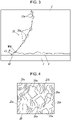
- Fig. 3 is a vertical sectional view of a side surface 21 of each metal plate 2 and a side surface 33 of the brazing material 3.
- Fig. 4 is an enlarged side view of a part of the side surface 21 of the metal plate 2.
- the metal plate 2 has a plurality of recessed portions 21a scattered over the side surface 21 thereof.
- the recessed portions 21a are portions recessed from the side surface 21 of the metal plate 2.
- the resin When a sealing resin is used, the resin extends into the recessed portions 21a so that the adhesion between the sealing resin (50) and the side surface 21 is improved. Since the side surface 21 has no projections that project from the surrounding regions, cracks extending from projections are not easily formed in the sealing resin, and the sealing reliability is high. In addition, the possibility that cracks will be formed in the sealing resin and that the insulation will be degraded due to electric discharge from projections in the cracks is low.
- the side surface 21 of the metal plate 2 has lines 21b in regions around the recessed portions 21a.
- the lines 21b are small irregularities (grooves), and therefore serve to further improve the adhesion of the resin.
- the lines 21b do not extend in the same direction, and therefore effectively improve the adhesion of the resin against stresses in every direction. In addition, since the lines 21b are short and have a small depth (height), cracks extending from the lines are not easily formed.
- the metal plate 2 is made of copper or a copper alloy, the conduction resistance can be reduced.
- the recessed portions 21a and the lines 21b can be easily formed by etching.
- the side surface 33 of the brazing material 3 may be continuous with the side surface 21 of the metal plate 2.
- the brazing material 3 is a silver-copper brazing alloy.
- the ratio of copper 3C on the side surface 33 of the brazing material 3 may be higher than the copper component ratio of the silver-copper brazing alloy. Since the ratio of silver on the side surface 33 of the brazing material 3 is low, migration of silver does not easily occur on the side surface of the brazing material 3. Therefore, two adjacent metal plates 2 and 2 can be reliably insulated from each other.
- each metal plate 2 Since the amount by which the brazing material 3 protrudes from the side surface 21 of each metal plate 2 is small and two adjacent metal plates 2 and 2 are joined with respective brazing materials 3 and 3 that are spaced from each other by a large distance, migration does not easily occur. Accordingly, the interval between the metal plates 2 and 2 can be reduced, so that the electric circuit board 10 and the power module can be reduced in size.
- the insulation between the adjacent metal plates (2, 2) and the adhesion between the side surface (21) of each metal plate and the sealing resin (50) can be improved.
- the side surface 33 of the brazing material 3 is continuous with the side surface 21 of the metal plate 2 so that the side surface 33 of the brazing material 3 is not displaced from the side surface 21 of the metal plate 2, nor does it overlap the side surface 21 of the metal plate 2.
- the side surface 21 of the metal plate 2 and the side surface 33 of the brazing material 3 are in contact with each other at a contact point P, at which a lower edge (P) of the side surface 21 of the metal plate 2 and an upper edge (P) of the side surface 33 of the brazing material 3 adjoin so that the side surface 21 of the metal plate 2 and the side surface 33 of the brazing material 3 form a single concave surface.
- the concave surface corresponds to a concave curve WS shown by the two-dot chain line in the vertical sectional view of Fig. 3 .
- the concave curve WS shows the side surface 21 of the metal plate 2 before the recessed portions 21a are formed.
- the side surface 21 of the metal plate 2 has a concave shape that extends substantially along the concave curve WS in regions excluding the recessed portions 21a.
- the recessed portions 21a are portions recessed from the concave surface (side surface 21) along the concave curve WS.
- the brazing material 3 Since the side surface 33 of the brazing material 3 is not displaced from the side surface 21 of the metal plate 2, the lower surface of the metal plate 2 is joined with the brazing material 3 over a region extending to the outer edge thereof. Thus, the brazing material 3 is appropriately joined to the metal plate 2.
- the amount by which the brazing material 3 protrudes sideways from the metal plate 2 is very small, and almost negligible. Therefore, the metal plate 2 and the metal plate 2 adjacent thereto have a sufficient gap therebetween.
- the concave surface formed by the side surface 21 of the metal plate 2 and the side surface 33 of the brazing material 3 is shaped to extend outward toward the bottom.
- the lower edge of the side surface 33 of the brazing material 3 is positioned outside the upper edge of the side surface 21 of the metal plate 2.
- the lower edge of the side surface 33 of the brazing material 3 extends outward beyond the metal plate 2, and an outer edge portion of the metal plate 2 is shaped such that the thickness thereof gradually decreases. Since the outer edge is shaped as described above, the thermal stress generated between the metal plate 2 and the insulating substrate 1 can be reduced, and the brazing material 3 is appropriately joined to the insulating substrate 1. Therefore, separation of the metal plate 2 does not easily occur at an end portion of the metal plate 2.
- the concave surface formed by the side surface 21 of the metal plate 2 and the side surface 33 of the brazing material 3 may be shaped to warp outward at the upper end of the side surface 21 of the metal plate 2.
- the upper surface of the metal plate 2 has a large area.
- the sealing resin (50) engages with the upper end portion of the side surface 21 of the metal plate 2, so that the possibility of separation is further reduced.
- the above-described shape of the metal plate 2 may be formed by performing grinding after a punching process, but may instead be easily formed by etching.
- the metal plate 2 may be appropriately joined to the insulating substrate 1, and a precise gap may be provided between the metal plate 2 and the metal plate 2 adjacent thereto.
- Examples of a method for forming the outline pattern of each metal plate 2 and joining the metal plates 2 to the insulating substrate 1 with the brazing material 3 include methods (A) and (B) described below.
- the patterning process may be either punching or etching.
- the patterned metal plates 2 may be placed on the insulating substrate 1 having brazing material paste for forming the brazing material 3 applied thereon, and then be heated so that the metal plates 2 are joined to the insulating substrate 1.
- the brazing material paste may be applied in patterns (hereinafter referred to also as patterned application) or be applied over the entire surface of the insulating substrate 1 (hereinafter referred to also as entire-surface application).
- the patterns thereof may be somewhat larger than the outline patterns of the metal plate 2 to allow for displacements.
- the brazing material paste may be applied either by entire-surface application or by patterned application.
- brazing material 3 When the brazing material 3 is applied by entire-surface application, it is not necessary to position the brazing material 3 with respect to the patterns of the metal plates 2. In either one of methods (A) and (B), when the brazing material 3 is applied by entire-surface application, a portion thereof formed between the metal plates 2 and 2 may be removed by etching to ensure insulation between the metal plates 2 and 2. Also when the brazing material 3 is to be formed such that the side surface 33 thereof is continuous with the side surface 21 of each metal plate 2, a portion of the brazing material 3 that protrudes from the pattern of the metal plate 2 may be removed by etching.
- Examples of a method for forming the recessed portions 21a in the side surface 21 of each metal plate 2 include methods (1) to (3) described below.
- the above-described pattern forming methods (A) and (B) and recessed-portion forming methods (1) to (3) may be applied in combinations.
- method (A) in which joining is performed after the patterning process, the recessed portions 21a may be formed either before or after the metal plates 2 are joined to the insulating substrate 1.
- the patterning process is punching, the recessed portions 21a are formed after the side surface 21 of each metal plate 2 is formed by, for example, grinding the side surface formed by the punching process and removing projections and the like to smooth the side surface.
- the manufacturing method 1 is based on the combination of pattern forming method (B) and recessed-portion forming method (3).
- the brazing material 3 is applied to the upper and lower surfaces of the insulating substrate 1 over the entire areas thereof by printing, and the metal plates 2 having the same size as that of the insulating substrate 1 in plan view are placed on the brazing material 3 and brazed to the insulating substrate 1 by applying pressure and heat.
- the insulating substrate 1 is composed of a ceramic sintered body.
- the metal plates 2 are made of copper or a copper alloy.
- the brazing material 3 is an active metal brazing material that is a silver-copper (Ag-Cu) brazing alloy containing titanium (Ti) as an active metal.
- each metal plate 2 is etched with an etchant, such as a ferric chloride solution, by using a resist mask placed on the upper surface of the metal plate 2 as a mask to form the metal plate 2 into desired circuit patterns.
- the etching conditions concentration of the etchant, etching time, etc. are adjusted so that the side surface 21 of the metal plate 2 is concave.
- the brazing material 3 is etched by alternately using two etchants.
- etching is performed by using a first solution.
- An etchant that mainly dissolves silver (Ag) and titanium (Ti) is selected as the first solution.
- an etchant containing hydrofluoric acid, aqueous hydrogen peroxide, and ammonia is used.
- etching is performed by using a second solution.
- An etchant that mainly dissolves copper (Cu) is selected as the second solution.
- an etchant containing sulfuric acid/aqueous hydrogen peroxide or a persulfate/sulfuric acid based etchant may be used.
- each metal plate 2 is made of copper, and is therefore also etched.
- a solution having different etching rates depending on the crystal orientation of copper is selected as the second solution.
- the etchant containing sulfuric acid/aqueous hydrogen peroxide has a high etching rate for the ⁇ 001 ⁇ plane of copper crystals, and the persulfate/sulfuric acid based etchant has a high etching rate for the ⁇ 327 ⁇ and ⁇ 425 ⁇ planes of copper crystals.
- the second etchant has an etching rate less than that of the above-described etchant such as ferric chloride. Therefore, the side surface 21 of each metal plate 2 formed by the etchant is hardly etched except for the portions having the above-described crystal orientations.
- Fig. 3 is a sectional view illustrating this state
- Fig. 4 is an enlarged schematic diagram illustrating a part of the side surface 21.
- the recessed portions 21a that are recessed from the side surface 21 of the metal plate 2 are scattered over the side surface 21 of the metal plate 2.
- the lines 21b are formed in the surface in regions around the recessed portions 21a.
- a large amount of copper 3C which is more difficult to etch than silver, remains on the side surface 33 of the brazing material 3.
- the above-described side surface 33 of the brazing material 3 on which the ratio of copper is higher than the copper component ratio of the silver-copper brazing alloy is formed.
- the amount of copper 3C on the side surface 33 can be more easily increased.
- An increase in the melting point due to an increase in the amount of copper can be reduced by adding indium (In), tin (Sn), zinc (Zn), antimony (Sb), or bismuth (Bi) .
- the side surfaces of the metal plate 2 and the brazing material 3 illustrated in Figs. 3 and 4 can be easily formed by the above-described manufacturing method 1.
- the outline patterns of the metal plate 2 and the brazing material 3 and the recessed portions 21a can be continuously and easily formed with high precision simply by changing the etching conditions (for example, etchants).
- Examples of power modules 100 illustrated in Figs. 5A and 5B , 6A, and 6B may be formed by mounting an electronic component 40 on the above-described electric circuit board 10 and sealing the electronic component 40 and other components with the sealing resin 50.
- Figs. 5A and 5B illustrate a state in which the sealing resin 50 is removed to clearly show the structure in which the electronic component 40 is mounted on one metal plate 2 (121) and connected to other metal plates 2 (122) with bonding wires 41.
- the power module 100 may be applied to, for example, an automobile and used in an engine control unit (ECU) or various other control units such as those for a power assisted steering wheel and a motor drive.
- the power module 100 is not limited to those used in control units mounted in automobiles, and may instead be used in, for example, various other inverter control circuits, electric power control circuits, and power conditioners.
- a single electronic component 40 is mounted on the metal plate 2 (121) joined to a central portion of a surface (upper surface) of the ceramic substrate (1).
- the metal plates 2 (122) arranged on both sides of the metal plate 2 (121) having the electronic component 40 mounted thereon are electrically connected to the electronic component 40 with the bonding wires 41.
- the metal plates 2 (122) on the outer sides function as terminals for providing connection to an external electric circuit.
- Heat generated by the electronic component 40 is transmitted to a metal plate 2 (123) joined to the lower surface of the ceramic substrate (1) through the metal plates 2 (121 and 122) joined to the upper surface of the ceramic substrate (1) and the ceramic substrate (1), and is dissipated to the outside.
- the metal plate 2 (123) joined to the lower surface of the ceramic substrate (1) functions as a heat dissipating plate.
- the number of electronic components 40 and the size and mounting position of each electronic component 40 are not limited to those in the examples illustrated in Figs. 5A and 5B , 6A, and 6B.
- the electronic component 40 is, for example, a power semiconductor device, and is used to control electric power in various types of control units such as those described above.
- Examples of the electronic component 40 include a transistor, such as a metal oxide semiconductor-field effect transistor (MOS-FET) or an IGBT in which Si is used, and a power device in which SiC or GaN is used.
- MOS-FET metal oxide semiconductor-field effect transistor
- IGBT IGBT
- SiC or GaN power device in which SiC or GaN is used.
- the electronic component 40 is joined and fixed to the corresponding metal plate 2 on the electric circuit board 10 by a joining material (not illustrated).
- the joining material may be, for example, solder or silver nano-paste.
- a metal film is provided on a portion of a surface of the metal plate 2, the size of the electronic component 40 may be less than that of the metal film in plan view.
- a fillet of the joining material is formed to extend from a side surface of the electronic component 40 to the upper surface of the metal film, so that the joining strength between the electronic component 40 and the metal plate 2 (metal film) can be increased.
- the adhesion of the sealing resin 50 described below can be improved.
- the bonding wires 41 are connecting members that electrically connect terminal electrodes (not illustrated) of the electronic component 40 to the metal plates 2.
- the bonding wires 41 may be made of, for example, gold or aluminum.
- a power module 101 illustrated in Fig. 6A is a power module including the electric circuit board 10 illustrated in Figs. 1A, 1B , 2A, and 2B .
- the electronic component 40 is sealed by being covered with the sealing resin 50 that spreads from the upper surface of the electric circuit board 10 to an outer peripheral portion of the lower surface of the electric circuit board 10.
- the sealing resin 50 does not cover a principal surface (lower surface) of the metal plate 2 (123) joined to the lower surface of the ceramic substrate (1). Therefore, the metal plate 2 (123), which functions as a heat dissipating plate, may be directly thermally connected to, for example, an external heat dissipating body. Accordingly, the power module 101 has a high heat dissipation performance.
- the metal plates 2 (122) that function as terminals are long enough to protrude from the insulating substrate 1, and also protrude from the sealing resin 50. Accordingly, the metal plates 2 (122) that function as terminals can be easily electrically connected to an external electric circuit.
- the sealing resin 50 may be a thermosetting resin such as silicone resin, epoxy resin, phenolic resin, or imide resin in consideration of thermal conductivity, insulation performance, environmental resistance, and sealing performance.
- a power module 102 illustrated in Fig. 6B is a power module including the electric circuit board 10 that is similar to the electric circuit board 10 included in the power module 100 illustrated in Figs. 5A and 5B .
- the electric circuit board 10 is disposed in an internal space of a housing 60 having an inner space, and the internal space is filled with the sealing resin 50 so that the electronic component 40 and the electric circuit board 10 are sealed.
- the power modules 101 and 102 may include the sealing resin 50 that covers the electronic component 40, the metal plates 2, and the insulating substrate 1.
- the sealing resin 50 serves to increase the environmental resistance of the electronic component 40 and improve the insulation between the metal plates 121 and 122 that are adjacent to each other.
- the housing 60 includes a frame 61 and a heat dissipating plate 62 that covers an opening at one side of the frame 61.
- the space surrounded by the frame 61 and the heat dissipating plate 62 serves as the inner space.
- Lead terminals 63 are arranged to extend from the inner space to the outside through the frame 61 of the housing 60. End portions of the lead terminals 63 disposed in the internal space are connected to the metal plates 2 of the electric circuit board 10 with the bonding wires 41.
- the electronic component 40 is electrically connectable to an external electric circuit.
- the frame 61 is made of a resin material, a metal material, or a mixture thereof, and the heat dissipating plate 62 covers the opening at one side of the frame 61 to form the inner space in which the electric circuit board 10 is disposed.
- the material of the frame 61 may be a metal material, such as copper or aluminum, or a resin material, such as polybutylene terephthalate (PBT) or polyphenylene sulfide (PPS) in consideration of heat dissipation performance, heat resistance, environmental resistance, and lightness.
- PBT polybutylene terephthalate
- PPS polyphenylene sulfide
- a PBT resin is preferred for its availability.
- a fiber reinforced resin is preferably formed by adding glass fiber to the PBT resin to increase the mechanical strength.
- the lead terminals 63 are conductive terminals attached to the frame 61 such that the lead terminals 63 extend from the inner space to the outside through the frame 61.
- the end portions of the lead terminals 63 in the inner space are electrically connected to the metal plates 2 of the electric circuit board 10, and outer end portions of the lead terminals 63 are electrically connected to an external electric circuit (not shown) or a power supply (not shown).
- the lead terminals 63 may be made of various metal materials for conductive terminals, such as Cu, a Cu alloy, Al, an Al alloy, Fe, a Fe alloy, and stainless steel (SUS).
- the heat dissipating plate 62 is provided to dissipate heat generated by the electronic component 40 in operation to the outside of the power module 102.
- the heat dissipating plate 62 may be made of a highly thermally conductive material, such as Al, Cu, or Cu-W.
- Al has a higher thermal conductivity and more efficiently dissipates heat generated by the electronic component 40 to the outside of the power module 102 compared to a metal material, such as Fe, that serves as a common structural material. Accordingly, the electronic component 40 reliably performs normal operations.
- Al is more easily available and less expensive compared to other highly thermally conductive materials, such as Cu and Cu-W, and is therefore advantageous in that the cost of the power module 102 can be reduced.
- the heat dissipating plate 62 is thermally connected to the metal plate 2 (123) of the electric circuit board 10 with a heat-transferring joining material (not illustrated).
- the heat-transferring joining material may be a brazing material that provides thermal connection along with a high mechanical joining strength, or grease that provides thermal connection with a relatively low mechanical joining strength.
- the sealing resin 50 may be used as described below.
- the sealing resin 50 fills the inner space to seal and protect the electronic component 40 mounted on the electric circuit board 10.
- the same sealing resin 50 that seals the inner space may be used also to mechanically join the electric circuit board 10 and the heat dissipating plate 62 together. In such a case, the electric circuit board 10 and the heat dissipating plate 62 can be mechanically strongly joined together and the inner space can be sealed with resin in the same process.
- the power module 102 may also have a cooling device 70 joined to an exposed surface of the heat dissipating plate 62 with a heat-transferring joining material 71 provided therebetween at a side opposite to the side at which the electric circuit board 10 is joined.
- the heat-transferring joining material 71 may be a material similar to the heat-transferring joining material with which the heat dissipating plate 62 is connected to the metal plate 2 (123) of the electric circuit board 10.
- the cooling device 70 is a block body made of a metal, for example, and having flow passages for allowing refrigerant, such as water, to pass therethrough.
- the cooling device 70 may instead be composed of, for example, a cooling fin.
- the cooling device 70 may also be applied to the power modules 100, 101 of the examples illustrated in Figs. 5A and 5B and Fig. 6A by connecting the cooling device 70 to the metal plate 2 (123) of the electric circuit board 10.
- the cooling device 70 may instead be such that only the heat dissipating plate 62 illustrated in Fig. 6B , which is flat plate-shaped, is used as the cooling device 70.
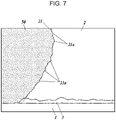
- the sealing resin 50 that covers the electronic component 40, the metal plates 2, the insulating substrate 1, and other components is joined also to the side surface 21 of each metal plate 2 such that the sealing resin 50 extends into the recessed portions 21a.
- the sealing resin 50 extends into the recessed portions 21a, the adhesion of the sealing resin 50 is improved. As a result, separation of the sealing resin 50 does not easily occur at high temperatures, and the heat resistance is increased accordingly.
- the metal plates 2 are provided on both sides of the insulating substrate 1.
- an electric circuit board may instead be formed by arranging the metal plates 2 only on one side of the insulating substrate 1.
- the electric circuit board 10 may be produced by forming a so-called multi-piece structure and then dividing the multi-piece structure.
- a multi-piece electric circuit board may be produced by preparing a large insulating substrate having a plurality of substrate regions, each of which corresponds to the insulating substrate 1 of the electric circuit board 10, and forming the metal plates 2 on each of the substrate regions by the above-described method.
- pattern forming method (B) is applied, a metal plate having substantially the same size as the size of the large insulating substrate may be used as the large metal plate.
- the present disclosure may be applied to an electric circuit board and a power module.
Landscapes
- Engineering & Computer Science (AREA)
- Microelectronics & Electronic Packaging (AREA)
- Chemical & Material Sciences (AREA)
- Ceramic Engineering (AREA)
- Manufacturing & Machinery (AREA)
- Materials Engineering (AREA)
- Structural Engineering (AREA)
- Organic Chemistry (AREA)
- Cooling Or The Like Of Semiconductors Or Solid State Devices (AREA)
- Structure Of Printed Boards (AREA)
Abstract
Description
- The present disclosure relates to an electric circuit board in which a metal plate that serves as a wiring material is joined to an insulating substrate with a brazing material, and a power module including the electric circuit board.
- An electric circuit board is used in an electronic device, such as a power module, in which an electronic component, such as an insulated gate bipolar transistor (IGBT), is mounted. A known example of such an electric circuit board includes an insulating substrate composed of, for example, a ceramic sintered body and metal plates made of a metal material, such as copper, that are joined to an upper surface of the insulating substrate.
- The metal plates may be produced by a punching process so that the metal plates have side surfaces perpendicular to the upper surface of the insulating substrate. Thus, the metal plates may be arranged with smaller intervals (narrower gaps) therebetween (between the side surfaces thereof) (see, for example,
Japanese Unexamined Patent Application Publication No. 2007-53349 - The metal plates may be joined to the insulating substrate by placing the metal plates on the insulating substrate with a brazing material applied between each metal plate and the insulating substrate and performing a brazing process.
-
Japanese Unexamined Patent Application Publication No. 2014-72304 - An electric circuit board according to an aspect of present disclosure includes an insulating substrate, a metal plate, and a brazing material with which the insulating substrate and the metal plate are joined together. The metal plate has a side surface over which a plurality of recessed portions are scattered.
-
- [
Fig. 1A] Fig. 1A is a perspective view of an example of an electric circuit board. - [
Fig. 1B] Fig. 1B is another perspective view of the example of an electric circuit board. - [
Fig. 2A] Fig. 2A is a top view of a power module illustrated inFigs. 1A and 1B . - [
Fig. 2B] Fig. 2B is a sectional view ofFig. 2A taken along line B-B. - [
Fig. 3] Fig. 3 is a vertical sectional view of a part of the electric circuit board. - [
Fig. 4] Fig. 4 is an enlarged side view of a part of a side surface of the metal plate. - [
Fig. 5A] Fig. 5A is a top view of a power module. - [
Fig. 5B] Fig. 5B is a sectional view ofFig. 5A taken along line B-B. - [
Fig. 6A] Fig. 6A is a sectional view of another example of a power module. - [
Fig. 6B] Fig. 6B is a sectional view of another example of a power module. - [
Fig. 7] Fig. 7 is a vertical sectional view of a part of a power module. - Electric circuit boards and power modules according to an embodiment of the present disclosure will now be described with reference to the drawings. In the following description, upper and lower sides are referred to for convenience, but do not limit the actual upper and lower sides of the electric circuit board in use.
- As illustrated in
Figs. 1A, 1B ,2A, and 2B , anelectric circuit board 10 according to the present embodiment includes aninsulating substrate 1 andmetal plates 2 joined to principal surfaces (upper and lower surfaces) of theinsulating substrate 1 with abrazing material 3.Multiple metal plates insulating substrate 1, and asingle metal plate 2 is joined to the lower surface of theinsulating substrate 1. - Preferably, the
insulating substrate 1 is composed of a ceramic sintered body and has a high mechanical strength and good heat transfer characteristics (cooling characteristics). The ceramic sintered body may be made of a known material and may be, for example, an alumina (Al2O3) sintered body, an aluminum nitride (AlN) sintered body, a silicon nitride (Si3N4) sintered body, or a silicon carbide (SiC) sintered body. Theinsulating substrate 1 may be manufactured by a known manufacturing method, for example, by preparing raw material powder composed of alumina powder to which a sintering additive is added, kneading the raw material powder together with, for example, an organic binder into the shape of a substrate, and firing the substrate. - In the present embodiment, the
metal plates 2 are made of copper (Cu) or a copper alloy. Thebrazing material 3 may be an active metal brazing material that is a silver-copper (Ag-Cu) brazing alloy containing an active metal, such as titanium (Ti), hafnium (Hf), or zirconium (Zr). When themetal plates 2 are made of aluminum (Al) or an aluminum alloy, a brazing material composed of an Al-Si based alloy or an Al-Ge based alloy may be used. - Each
metal plate 2 may have a plating layer provided on a surface thereof to protect the surface or to facilitate joining of, for example, a bonding wire thereto. The plating layer may be a metal plating layer made of, for example, palladium, nickel, or silver. -
Fig. 3 is a vertical sectional view of aside surface 21 of eachmetal plate 2 and aside surface 33 of thebrazing material 3.Fig. 4 is an enlarged side view of a part of theside surface 21 of themetal plate 2. - The
metal plate 2 has a plurality of recessedportions 21a scattered over theside surface 21 thereof. The recessedportions 21a are portions recessed from theside surface 21 of themetal plate 2. - When a sealing resin is used, the resin extends into the
recessed portions 21a so that the adhesion between the sealing resin (50) and theside surface 21 is improved. Since theside surface 21 has no projections that project from the surrounding regions, cracks extending from projections are not easily formed in the sealing resin, and the sealing reliability is high. In addition, the possibility that cracks will be formed in the sealing resin and that the insulation will be degraded due to electric discharge from projections in the cracks is low. - As illustrated in
Fig. 4 , theside surface 21 of themetal plate 2 haslines 21b in regions around the recessedportions 21a. - The
lines 21b are small irregularities (grooves), and therefore serve to further improve the adhesion of the resin. - The
lines 21b do not extend in the same direction, and therefore effectively improve the adhesion of the resin against stresses in every direction. In addition, since thelines 21b are short and have a small depth (height), cracks extending from the lines are not easily formed. - When the
metal plate 2 is made of copper or a copper alloy, the conduction resistance can be reduced. In addition, as described below, the recessedportions 21a and thelines 21b can be easily formed by etching. - As illustrated in
Fig. 3 , theside surface 33 of thebrazing material 3 may be continuous with theside surface 21 of themetal plate 2. When themetal plate 2 is made of copper or a copper alloy, thebrazing material 3 is a silver-copper brazing alloy. In this case, the ratio ofcopper 3C on theside surface 33 of thebrazing material 3 may be higher than the copper component ratio of the silver-copper brazing alloy. Since the ratio of silver on theside surface 33 of thebrazing material 3 is low, migration of silver does not easily occur on the side surface of thebrazing material 3. Therefore, twoadjacent metal plates brazing material 3 protrudes from theside surface 21 of eachmetal plate 2 is small and twoadjacent metal plates respective brazing materials metal plates electric circuit board 10 and the power module can be reduced in size. - As described above, according to the electric circuit board (10) of the present embodiment, the insulation between the adjacent metal plates (2, 2) and the adhesion between the side surface (21) of each metal plate and the sealing resin (50) can be improved.
- As illustrated in
Fig. 3 , theside surface 33 of thebrazing material 3 is continuous with theside surface 21 of themetal plate 2 so that theside surface 33 of thebrazing material 3 is not displaced from theside surface 21 of themetal plate 2, nor does it overlap theside surface 21 of themetal plate 2. - Referring to
Fig. 3 , theside surface 21 of themetal plate 2 and theside surface 33 of thebrazing material 3 are in contact with each other at a contact point P, at which a lower edge (P) of theside surface 21 of themetal plate 2 and an upper edge (P) of theside surface 33 of thebrazing material 3 adjoin so that theside surface 21 of themetal plate 2 and theside surface 33 of thebrazing material 3 form a single concave surface. The concave surface corresponds to a concave curve WS shown by the two-dot chain line in the vertical sectional view ofFig. 3 . The concave curve WS shows theside surface 21 of themetal plate 2 before the recessedportions 21a are formed. Also after the recessedportions 21a are formed, theside surface 21 of themetal plate 2 has a concave shape that extends substantially along the concave curve WS in regions excluding the recessedportions 21a. The recessedportions 21a are portions recessed from the concave surface (side surface 21) along the concave curve WS. - Since the
side surface 33 of thebrazing material 3 is not displaced from theside surface 21 of themetal plate 2, the lower surface of themetal plate 2 is joined with thebrazing material 3 over a region extending to the outer edge thereof. Thus, thebrazing material 3 is appropriately joined to themetal plate 2. - The amount by which the
brazing material 3 protrudes sideways from themetal plate 2 is very small, and almost negligible. Therefore, themetal plate 2 and themetal plate 2 adjacent thereto have a sufficient gap therebetween. - The concave surface formed by the
side surface 21 of themetal plate 2 and theside surface 33 of thebrazing material 3 is shaped to extend outward toward the bottom. The lower edge of theside surface 33 of thebrazing material 3 is positioned outside the upper edge of theside surface 21 of themetal plate 2. As illustrated inFig. 3 , the lower edge of theside surface 33 of thebrazing material 3 extends outward beyond themetal plate 2, and an outer edge portion of themetal plate 2 is shaped such that the thickness thereof gradually decreases. Since the outer edge is shaped as described above, the thermal stress generated between themetal plate 2 and the insulatingsubstrate 1 can be reduced, and thebrazing material 3 is appropriately joined to the insulatingsubstrate 1. Therefore, separation of themetal plate 2 does not easily occur at an end portion of themetal plate 2. - The concave surface formed by the
side surface 21 of themetal plate 2 and theside surface 33 of thebrazing material 3 may be shaped to warp outward at the upper end of theside surface 21 of themetal plate 2. In such a case, the upper surface of themetal plate 2 has a large area. In addition, the sealing resin (50) engages with the upper end portion of theside surface 21 of themetal plate 2, so that the possibility of separation is further reduced. - The above-described shape of the
metal plate 2 may be formed by performing grinding after a punching process, but may instead be easily formed by etching. - As described above, the
metal plate 2 may be appropriately joined to the insulatingsubstrate 1, and a precise gap may be provided between themetal plate 2 and themetal plate 2 adjacent thereto. - A method for manufacturing the electric circuit board will now be described.
- Examples of a method for forming the outline pattern of each
metal plate 2 and joining themetal plates 2 to the insulatingsubstrate 1 with thebrazing material 3 include methods (A) and (B) described below. - (A) Method of patterning the
metal plates 2 and then joining themetal plates 2 to the insulatingsubstrate 1. - The patterning process may be either punching or etching. The patterned
metal plates 2 may be placed on the insulatingsubstrate 1 having brazing material paste for forming thebrazing material 3 applied thereon, and then be heated so that themetal plates 2 are joined to the insulatingsubstrate 1. - The brazing material paste may be applied in patterns (hereinafter referred to also as patterned application) or be applied over the entire surface of the insulating substrate 1 (hereinafter referred to also as entire-surface application).
- When the brazing material paste is applied in patterns, the patterns thereof may be somewhat larger than the outline patterns of the
metal plate 2 to allow for displacements. - (B) Method of joining a large metal plate and then patterning the metal plate by etching.
- The brazing material paste may be applied either by entire-surface application or by patterned application.
- When the
brazing material 3 is applied by entire-surface application, it is not necessary to position thebrazing material 3 with respect to the patterns of themetal plates 2. In either one of methods (A) and (B), when thebrazing material 3 is applied by entire-surface application, a portion thereof formed between themetal plates metal plates brazing material 3 is to be formed such that theside surface 33 thereof is continuous with theside surface 21 of eachmetal plate 2, a portion of thebrazing material 3 that protrudes from the pattern of themetal plate 2 may be removed by etching. - Examples of a method for forming the recessed
portions 21a in theside surface 21 of eachmetal plate 2 include methods (1) to (3) described below. - (1) Method of forming the recessed
portions 21a in theside surface 21 of themetal plate 2 by stamping. - (2) Method of performing etching using a mask pattern having openings at positions where the recessed
portions 21a are to be formed in theside surface 21 of themetal plate 2. - (3) Method of performing etching using an etchant that selectively etches portions of the
side surface 21 of themetal plate 2. - The above-described pattern forming methods (A) and (B) and recessed-portion forming methods (1) to (3) may be applied in combinations. When method (A), in which joining is performed after the patterning process, the recessed
portions 21a may be formed either before or after themetal plates 2 are joined to the insulatingsubstrate 1. When the patterning process is punching, the recessedportions 21a are formed after theside surface 21 of eachmetal plate 2 is formed by, for example, grinding the side surface formed by the punching process and removing projections and the like to smooth the side surface. - An example of a method for manufacturing the electric circuit board (manufacturing method 1) based on combinations of the above-described pattern forming methods and recessed-portion forming methods will now be disclosed. The
manufacturing method 1 is based on the combination of pattern forming method (B) and recessed-portion forming method (3). - First, the
brazing material 3 is applied to the upper and lower surfaces of the insulatingsubstrate 1 over the entire areas thereof by printing, and themetal plates 2 having the same size as that of the insulatingsubstrate 1 in plan view are placed on thebrazing material 3 and brazed to the insulatingsubstrate 1 by applying pressure and heat. The insulatingsubstrate 1 is composed of a ceramic sintered body. Themetal plates 2 are made of copper or a copper alloy. Thebrazing material 3 is an active metal brazing material that is a silver-copper (Ag-Cu) brazing alloy containing titanium (Ti) as an active metal. - After that, each
metal plate 2 is etched with an etchant, such as a ferric chloride solution, by using a resist mask placed on the upper surface of themetal plate 2 as a mask to form themetal plate 2 into desired circuit patterns. The etching conditions (concentration of the etchant, etching time, etc.) are adjusted so that theside surface 21 of themetal plate 2 is concave. - Next, a portion of the
brazing material 3 that protrudes from the outline of eachmetal plate 2 is removed by etching in the following manner. - That is, the
brazing material 3 is etched by alternately using two etchants. - First, etching is performed by using a first solution.
- An etchant that mainly dissolves silver (Ag) and titanium (Ti) is selected as the first solution. For example, an etchant containing hydrofluoric acid, aqueous hydrogen peroxide, and ammonia is used.
- During etching with the first solution, dissolution of silver and titanium contained in the silver-copper-alloy active metal brazing material progresses in the region between the
metal plates - Next, etching is performed by using a second solution. An etchant that mainly dissolves copper (Cu) is selected as the second solution. For example, an etchant containing sulfuric acid/aqueous hydrogen peroxide or a persulfate/sulfuric acid based etchant may be used.
- During etching with the second solution, dissolution of copper contained in the silver-copper brazing alloy progresses. The
side surface 21 of eachmetal plate 2 is made of copper, and is therefore also etched. A solution having different etching rates depending on the crystal orientation of copper is selected as the second solution. The etchant containing sulfuric acid/aqueous hydrogen peroxide has a high etching rate for the {001} plane of copper crystals, and the persulfate/sulfuric acid based etchant has a high etching rate for the {327} and {425} planes of copper crystals. Therefore, copper crystals having easily etched crystal faces exposed at theside surface 21 are dissolved to form the recessedportions 21a in the side surface 21 (Fig. 3 ). The second etchant has an etching rate less than that of the above-described etchant such as ferric chloride. Therefore, theside surface 21 of eachmetal plate 2 formed by the etchant is hardly etched except for the portions having the above-described crystal orientations. - The etching with the first solution and the etching with the second solution are alternately performed to remove the portion of the
brazing material 3 that protrudes from eachmetal plate 2 so that the insulatingsubstrate 1 is exposed.Fig. 3 is a sectional view illustrating this state, andFig. 4 is an enlarged schematic diagram illustrating a part of theside surface 21. The recessedportions 21a that are recessed from theside surface 21 of themetal plate 2 are scattered over theside surface 21 of themetal plate 2. As illustrated inFig. 3 , as a result of the etching with the first solution and the etching with the second solution being alternately performed, thelines 21b are formed in the surface in regions around the recessedportions 21a. - In addition, as illustrated in
Fig. 3 , a large amount ofcopper 3C, which is more difficult to etch than silver, remains on theside surface 33 of thebrazing material 3. Thus, the above-describedside surface 33 of thebrazing material 3 on which the ratio of copper is higher than the copper component ratio of the silver-copper brazing alloy is formed. When the composition of thebrazing material 3 is slightly out of eutectic composition such that the amount of copper is increased to increase the ratio of copper, the amount ofcopper 3C on theside surface 33 can be more easily increased. An increase in the melting point due to an increase in the amount of copper can be reduced by adding indium (In), tin (Sn), zinc (Zn), antimony (Sb), or bismuth (Bi) . - The side surfaces of the
metal plate 2 and thebrazing material 3 illustrated inFigs. 3 and 4 can be easily formed by the above-describedmanufacturing method 1. The outline patterns of themetal plate 2 and thebrazing material 3 and the recessedportions 21a can be continuously and easily formed with high precision simply by changing the etching conditions (for example, etchants). - Examples of
power modules 100 illustrated inFigs. 5A and 5B ,6A, and 6B may be formed by mounting anelectronic component 40 on the above-describedelectric circuit board 10 and sealing theelectronic component 40 and other components with the sealingresin 50.Figs. 5A and 5B illustrate a state in which the sealingresin 50 is removed to clearly show the structure in which theelectronic component 40 is mounted on one metal plate 2 (121) and connected to other metal plates 2 (122) withbonding wires 41. Thepower module 100 may be applied to, for example, an automobile and used in an engine control unit (ECU) or various other control units such as those for a power assisted steering wheel and a motor drive. Thepower module 100 is not limited to those used in control units mounted in automobiles, and may instead be used in, for example, various other inverter control circuits, electric power control circuits, and power conditioners. - In each of the examples of
power modules 100 illustrated inFigs. 5A and 5B ,6A, and 6B , a singleelectronic component 40 is mounted on the metal plate 2 (121) joined to a central portion of a surface (upper surface) of the ceramic substrate (1). The metal plates 2 (122) arranged on both sides of the metal plate 2 (121) having theelectronic component 40 mounted thereon are electrically connected to theelectronic component 40 with thebonding wires 41. The metal plates 2 (122) on the outer sides function as terminals for providing connection to an external electric circuit. Heat generated by theelectronic component 40 is transmitted to a metal plate 2 (123) joined to the lower surface of the ceramic substrate (1) through the metal plates 2 (121 and 122) joined to the upper surface of the ceramic substrate (1) and the ceramic substrate (1), and is dissipated to the outside. Thus, the metal plate 2 (123) joined to the lower surface of the ceramic substrate (1) functions as a heat dissipating plate. The number ofelectronic components 40 and the size and mounting position of eachelectronic component 40 are not limited to those in the examples illustrated inFigs. 5A and 5B ,6A, and 6B. - The
electronic component 40 is, for example, a power semiconductor device, and is used to control electric power in various types of control units such as those described above. Examples of theelectronic component 40 include a transistor, such as a metal oxide semiconductor-field effect transistor (MOS-FET) or an IGBT in which Si is used, and a power device in which SiC or GaN is used. - The
electronic component 40 is joined and fixed to the correspondingmetal plate 2 on theelectric circuit board 10 by a joining material (not illustrated). The joining material may be, for example, solder or silver nano-paste. When a metal film is provided on a portion of a surface of themetal plate 2, the size of theelectronic component 40 may be less than that of the metal film in plan view. In such a case, a fillet of the joining material is formed to extend from a side surface of theelectronic component 40 to the upper surface of the metal film, so that the joining strength between theelectronic component 40 and the metal plate 2 (metal film) can be increased. In addition, since the surface of the metal film is covered by the joining material and is not exposed, the adhesion of the sealingresin 50 described below can be improved. - The
bonding wires 41 are connecting members that electrically connect terminal electrodes (not illustrated) of theelectronic component 40 to themetal plates 2. Thebonding wires 41 may be made of, for example, gold or aluminum. - A
power module 101 illustrated inFig. 6A is a power module including theelectric circuit board 10 illustrated inFigs. 1A, 1B ,2A, and 2B . In this example, theelectronic component 40 is sealed by being covered with the sealingresin 50 that spreads from the upper surface of theelectric circuit board 10 to an outer peripheral portion of the lower surface of theelectric circuit board 10. The sealingresin 50 does not cover a principal surface (lower surface) of the metal plate 2 (123) joined to the lower surface of the ceramic substrate (1). Therefore, the metal plate 2 (123), which functions as a heat dissipating plate, may be directly thermally connected to, for example, an external heat dissipating body. Accordingly, thepower module 101 has a high heat dissipation performance. The metal plates 2 (122) that function as terminals are long enough to protrude from the insulatingsubstrate 1, and also protrude from the sealingresin 50. Accordingly, the metal plates 2 (122) that function as terminals can be easily electrically connected to an external electric circuit. - The sealing
resin 50 may be a thermosetting resin such as silicone resin, epoxy resin, phenolic resin, or imide resin in consideration of thermal conductivity, insulation performance, environmental resistance, and sealing performance. - A
power module 102 illustrated inFig. 6B is a power module including theelectric circuit board 10 that is similar to theelectric circuit board 10 included in thepower module 100 illustrated inFigs. 5A and 5B . In this example, theelectric circuit board 10 is disposed in an internal space of ahousing 60 having an inner space, and the internal space is filled with the sealingresin 50 so that theelectronic component 40 and theelectric circuit board 10 are sealed. - As in the examples illustrated in
Figs. 5A and 5B ,6A, and 6B , thepower modules resin 50 that covers theelectronic component 40, themetal plates 2, and the insulatingsubstrate 1. The sealingresin 50 serves to increase the environmental resistance of theelectronic component 40 and improve the insulation between the metal plates 121 and 122 that are adjacent to each other. - The
housing 60 includes aframe 61 and aheat dissipating plate 62 that covers an opening at one side of theframe 61. The space surrounded by theframe 61 and theheat dissipating plate 62 serves as the inner space. Leadterminals 63 are arranged to extend from the inner space to the outside through theframe 61 of thehousing 60. End portions of thelead terminals 63 disposed in the internal space are connected to themetal plates 2 of theelectric circuit board 10 with thebonding wires 41. Thus, theelectronic component 40 is electrically connectable to an external electric circuit. - The
frame 61 is made of a resin material, a metal material, or a mixture thereof, and theheat dissipating plate 62 covers the opening at one side of theframe 61 to form the inner space in which theelectric circuit board 10 is disposed. The material of theframe 61 may be a metal material, such as copper or aluminum, or a resin material, such as polybutylene terephthalate (PBT) or polyphenylene sulfide (PPS) in consideration of heat dissipation performance, heat resistance, environmental resistance, and lightness. In particular, a PBT resin is preferred for its availability. In addition, a fiber reinforced resin is preferably formed by adding glass fiber to the PBT resin to increase the mechanical strength. - The
lead terminals 63 are conductive terminals attached to theframe 61 such that thelead terminals 63 extend from the inner space to the outside through theframe 61. The end portions of thelead terminals 63 in the inner space are electrically connected to themetal plates 2 of theelectric circuit board 10, and outer end portions of thelead terminals 63 are electrically connected to an external electric circuit (not shown) or a power supply (not shown). Thelead terminals 63 may be made of various metal materials for conductive terminals, such as Cu, a Cu alloy, Al, an Al alloy, Fe, a Fe alloy, and stainless steel (SUS). - The
heat dissipating plate 62 is provided to dissipate heat generated by theelectronic component 40 in operation to the outside of thepower module 102. Theheat dissipating plate 62 may be made of a highly thermally conductive material, such as Al, Cu, or Cu-W. In particular, Al has a higher thermal conductivity and more efficiently dissipates heat generated by theelectronic component 40 to the outside of thepower module 102 compared to a metal material, such as Fe, that serves as a common structural material. Accordingly, theelectronic component 40 reliably performs normal operations. Furthermore, Al is more easily available and less expensive compared to other highly thermally conductive materials, such as Cu and Cu-W, and is therefore advantageous in that the cost of thepower module 102 can be reduced. - The
heat dissipating plate 62 is thermally connected to the metal plate 2 (123) of theelectric circuit board 10 with a heat-transferring joining material (not illustrated). The heat-transferring joining material may be a brazing material that provides thermal connection along with a high mechanical joining strength, or grease that provides thermal connection with a relatively low mechanical joining strength. Alternatively, the sealingresin 50 may be used as described below. - The sealing
resin 50 fills the inner space to seal and protect theelectronic component 40 mounted on theelectric circuit board 10. Thesame sealing resin 50 that seals the inner space may be used also to mechanically join theelectric circuit board 10 and theheat dissipating plate 62 together. In such a case, theelectric circuit board 10 and theheat dissipating plate 62 can be mechanically strongly joined together and the inner space can be sealed with resin in the same process. - To further improve the heat dissipation characteristics, the
power module 102 may also have acooling device 70 joined to an exposed surface of theheat dissipating plate 62 with a heat-transferring joiningmaterial 71 provided therebetween at a side opposite to the side at which theelectric circuit board 10 is joined. The heat-transferring joiningmaterial 71 may be a material similar to the heat-transferring joining material with which theheat dissipating plate 62 is connected to the metal plate 2 (123) of theelectric circuit board 10. In the example illustrated inFig. 6B , thecooling device 70 is a block body made of a metal, for example, and having flow passages for allowing refrigerant, such as water, to pass therethrough. However, thecooling device 70 may instead be composed of, for example, a cooling fin. Thecooling device 70 may also be applied to thepower modules Figs. 5A and 5B andFig. 6A by connecting thecooling device 70 to the metal plate 2 (123) of theelectric circuit board 10. In such a case, thecooling device 70 may instead be such that only theheat dissipating plate 62 illustrated inFig. 6B , which is flat plate-shaped, is used as thecooling device 70. - In the above-described power modules, as illustrated in
Fig. 7 , the sealingresin 50 that covers theelectronic component 40, themetal plates 2, the insulatingsubstrate 1, and other components is joined also to theside surface 21 of eachmetal plate 2 such that the sealingresin 50 extends into the recessedportions 21a. - Since the sealing
resin 50 extends into the recessedportions 21a, the adhesion of the sealingresin 50 is improved. As a result, separation of the sealingresin 50 does not easily occur at high temperatures, and the heat resistance is increased accordingly. - Although embodiments of the present disclosure have been described, the embodiments are illustrative, and various other embodiments are also possible. The components may be omitted, replaced, or altered without departing from the gist of the invention.
- In the above-described embodiments, the
metal plates 2 are provided on both sides of the insulatingsubstrate 1. However, an electric circuit board may instead be formed by arranging themetal plates 2 only on one side of the insulatingsubstrate 1. Theelectric circuit board 10 may be produced by forming a so-called multi-piece structure and then dividing the multi-piece structure. A multi-piece electric circuit board may be produced by preparing a large insulating substrate having a plurality of substrate regions, each of which corresponds to the insulatingsubstrate 1 of theelectric circuit board 10, and forming themetal plates 2 on each of the substrate regions by the above-described method. When pattern forming method (B) is applied, a metal plate having substantially the same size as the size of the large insulating substrate may be used as the large metal plate. - The present disclosure may be applied to an electric circuit board and a power module.
-
- 1
- insulating substrate
- 2
- metal plate
- 3
- brazing material
- 3C
- copper on side surface of brazing material
- 10
- electric circuit board
- 21
- side surface of metal plate
- 21a
- recessed portion
- 21b
- line
- 33
- side surface of brazing material
- 40
- electronic component
- 41
- bonding wire
- 50
- sealing resin
- 100
- power module
- 101
- power module
- 102
- power module
Claims (5)
- An electric circuit board comprising an insulating substrate, a metal plate, and a brazing material with which the insulating substrate and the metal plate are joined together,
wherein the metal plate has a side surface over which a plurality of recessed portions are scattered. - The electric circuit board according to Claim 1, wherein the side surface of the metal plate has lines in regions around the recessed portions.
- The electric circuit board according to Claim 1 or 2, wherein the metal plate is made of copper or a copper alloy.
- The electric circuit board according to Claim 3, wherein the brazing material has a side surface that is continuous with the side surface of the metal plate,wherein the brazing material is a silver-copper brazing alloy, andwherein a ratio of copper on the side surface of the brazing material is higher than a copper component ratio of the silver-copper brazing alloy.
- A power module comprising:the electric circuit board according to any one of Claims 1 to 4;an electronic component mounted on the metal plate of the electric circuit board; anda sealing resin that covers the electronic component, the metal plate, and the insulating substrate,wherein the sealing resin is joined to the side surface of the metal plate such that the sealing resin extends into the recessed portions.
Applications Claiming Priority (2)
| Application Number | Priority Date | Filing Date | Title |
|---|---|---|---|
| JP2019157199 | 2019-08-29 | ||
| PCT/JP2020/032109 WO2021039816A1 (en) | 2019-08-29 | 2020-08-26 | Electric circuit board and power module |
Publications (2)
| Publication Number | Publication Date |
|---|---|
| EP4024444A1 true EP4024444A1 (en) | 2022-07-06 |
| EP4024444A4 EP4024444A4 (en) | 2023-09-20 |
Family
ID=74684175
Family Applications (1)
| Application Number | Title | Priority Date | Filing Date |
|---|---|---|---|
| EP20858188.4A Pending EP4024444A4 (en) | 2019-08-29 | 2020-08-26 | Electric circuit board and power module |
Country Status (5)
| Country | Link |
|---|---|
| US (1) | US12349299B2 (en) |
| EP (1) | EP4024444A4 (en) |
| JP (1) | JP7221401B2 (en) |
| CN (1) | CN114303237A (en) |
| WO (1) | WO2021039816A1 (en) |
Families Citing this family (3)
| Publication number | Priority date | Publication date | Assignee | Title |
|---|---|---|---|---|
| JP7604987B2 (en) * | 2021-03-29 | 2024-12-24 | 沖電気工業株式会社 | SEMICONDUCTOR ELEMENT UNIT, SEMICONDUCTOR ELEMENT UNIT MANUFACTURING METHOD, SEMICONDUCTOR ELEMENT UNIT SUPPLY BOARD, SEMICONDUCTOR MOUNTING CIRCUIT, AND SEMICONDUCTOR MOUNTING CIRCUIT MANUFACTURING METHOD |
| US12238906B2 (en) | 2023-01-17 | 2025-02-25 | Toyota Motor Engineering & Manufacturing North America, Inc. | Power electronic device assemblies having heat spreaders and electrically insulating layer |
| DE102024203957A1 (en) | 2024-04-26 | 2025-04-03 | Vitesco Technologies Germany Gmbh | Electronic arrangement and inverter with an electronic arrangement |
Family Cites Families (27)
| Publication number | Priority date | Publication date | Assignee | Title |
|---|---|---|---|---|
| JPH06334077A (en) | 1993-05-21 | 1994-12-02 | Kyocera Corp | Package for containing semiconductor element |
| JP3512977B2 (en) * | 1996-08-27 | 2004-03-31 | 同和鉱業株式会社 | High reliability semiconductor substrate |
| JP3297006B2 (en) | 1997-12-05 | 2002-07-02 | イビデン株式会社 | Multilayer printed wiring board |
| JP3449458B2 (en) * | 1997-05-26 | 2003-09-22 | 電気化学工業株式会社 | Circuit board |
| JP2000261149A (en) | 1999-03-08 | 2000-09-22 | Ibiden Co Ltd | Mutilayer printed wiring board and manufacture thereof |
| JP5038565B2 (en) * | 2000-09-22 | 2012-10-03 | 株式会社東芝 | Ceramic circuit board and manufacturing method thereof |
| JP4811756B2 (en) * | 2001-09-28 | 2011-11-09 | Dowaメタルテック株式会社 | Method for manufacturing metal-ceramic bonding circuit board |
| JP2004034524A (en) | 2002-07-03 | 2004-02-05 | Mec Kk | Metal resin composite and method for producing the same |
| JP5151080B2 (en) | 2005-07-20 | 2013-02-27 | 三菱マテリアル株式会社 | Insulating substrate, method for manufacturing insulating substrate, power module substrate and power module |
| US8563869B2 (en) * | 2005-08-29 | 2013-10-22 | Hitachi Metals, Ltd. | Circuit board and semiconductor module using this, production method for circuit board |
| JP4904916B2 (en) * | 2006-05-18 | 2012-03-28 | 三菱マテリアル株式会社 | Power module substrate, power module substrate manufacturing method, and power module |
| US8018047B2 (en) * | 2007-08-06 | 2011-09-13 | Infineon Technologies Ag | Power semiconductor module including a multilayer substrate |
| US7821130B2 (en) * | 2008-03-31 | 2010-10-26 | Infineon Technologies Ag | Module including a rough solder joint |
| US8609993B2 (en) * | 2008-05-16 | 2013-12-17 | Mitsubishi Materials Corporation | Power module substrate, power module, and method for manufacturing power module substrate |
| CN102047413B (en) * | 2008-06-06 | 2015-04-15 | 三菱综合材料株式会社 | Substrate for power module, power module, and manufacturing method of substrate for power module |
| JP2011253950A (en) * | 2010-06-02 | 2011-12-15 | Mitsubishi Electric Corp | Power semiconductor device |
| JP5983249B2 (en) | 2012-09-28 | 2016-08-31 | サンケン電気株式会社 | Manufacturing method of semiconductor module |
| TWI489918B (en) * | 2012-11-23 | 2015-06-21 | 旭德科技股份有限公司 | Package carrier |
| JP6056432B2 (en) * | 2012-12-06 | 2017-01-11 | 三菱マテリアル株式会社 | Power module substrate, power module substrate with heat sink, power module, power module substrate manufacturing method |
| JP6111764B2 (en) * | 2013-03-18 | 2017-04-12 | 三菱マテリアル株式会社 | Power module substrate manufacturing method |
| JP6210818B2 (en) * | 2013-09-30 | 2017-10-11 | 三菱電機株式会社 | Semiconductor device and manufacturing method thereof |
| EP3200223B1 (en) * | 2014-09-26 | 2019-06-12 | Kyocera Corporation | Wiring board, electronic device and electronic module |
| EP3321957B1 (en) * | 2015-07-09 | 2022-07-27 | Kabushiki Kaisha Toshiba | Ceramic metal circuit board and semiconductor device using same |
| CN107251214B (en) * | 2015-09-28 | 2019-08-27 | 株式会社东芝 | Silicon nitride circuit board and semiconductor module using the same |
| WO2018021473A1 (en) * | 2016-07-28 | 2018-02-01 | 株式会社 東芝 | Circuit board and semiconductor module |
| JP6546892B2 (en) | 2016-09-26 | 2019-07-17 | 株式会社 日立パワーデバイス | Semiconductor device |
| JP7018756B2 (en) | 2017-12-11 | 2022-02-14 | 京セラ株式会社 | Power module board and power module |
-
2020
- 2020-08-26 US US17/639,184 patent/US12349299B2/en active Active
- 2020-08-26 JP JP2021542949A patent/JP7221401B2/en active Active
- 2020-08-26 EP EP20858188.4A patent/EP4024444A4/en active Pending
- 2020-08-26 CN CN202080060448.6A patent/CN114303237A/en active Pending
- 2020-08-26 WO PCT/JP2020/032109 patent/WO2021039816A1/en not_active Ceased
Also Published As
| Publication number | Publication date |
|---|---|
| US12349299B2 (en) | 2025-07-01 |
| CN114303237A (en) | 2022-04-08 |
| JP7221401B2 (en) | 2023-02-13 |
| WO2021039816A1 (en) | 2021-03-04 |
| EP4024444A4 (en) | 2023-09-20 |
| JPWO2021039816A1 (en) | 2021-03-04 |
| US20220330447A1 (en) | 2022-10-13 |
Similar Documents
| Publication | Publication Date | Title |
|---|---|---|
| JP4635564B2 (en) | Semiconductor device | |
| EP1995775B1 (en) | Semiconductor device with stress reducing element | |
| JP4438489B2 (en) | Semiconductor device | |
| EP3198640B1 (en) | Method of forming a semiconductor package | |
| KR102411122B1 (en) | Semiconductor package having heat protecting structure, semiconductor joined cooling system, substrate having heat protecting structure and method for fabricating substrate having heat protecting structure | |
| JP7483955B2 (en) | Power module substrate and power module | |
| CN110047807B (en) | Semiconductor device | |
| US12349299B2 (en) | Electric circuit board and power module | |
| CN113039636B (en) | Power semiconductor devices | |
| JP3390661B2 (en) | Power module | |
| JP2015005681A (en) | Semiconductor device and method of manufacturing the same | |
| WO2020027183A1 (en) | Electric circuit board and power module | |
| US11195775B2 (en) | Semiconductor module, semiconductor device, and manufacturing method of semiconductor module | |
| JP2017011216A (en) | Circuit board and electronic device | |
| CN114446899B (en) | Semiconductor device with a semiconductor device having a plurality of semiconductor chips | |
| WO2018018847A1 (en) | Intelligent power module and method for manufacturing same | |
| JP7018756B2 (en) | Power module board and power module | |
| CN115206891B (en) | A semiconductor circuit for improving the adhesion between the substrate and the sealing layer, and a method for manufacturing the same. | |
| WO2019163941A1 (en) | Substrate for power modules, and power module | |
| CN111834307B (en) | Semiconductor Module | |
| JP7170501B2 (en) | Substrates for power modules and power modules | |
| CN114203650A (en) | Semiconductor device and method for manufacturing semiconductor device | |
| JP2009164511A (en) | Semiconductor device and manufacturing method thereof | |
| JP2009010210A (en) | Semiconductor device and manufacturing method thereof | |
| TW202518706A (en) | Semiconductor device |
Legal Events
| Date | Code | Title | Description |
|---|---|---|---|
| STAA | Information on the status of an ep patent application or granted ep patent |
Free format text: STATUS: THE INTERNATIONAL PUBLICATION HAS BEEN MADE |
|
| PUAI | Public reference made under article 153(3) epc to a published international application that has entered the european phase |
Free format text: ORIGINAL CODE: 0009012 |
|
| STAA | Information on the status of an ep patent application or granted ep patent |
Free format text: STATUS: REQUEST FOR EXAMINATION WAS MADE |
|
| 17P | Request for examination filed |
Effective date: 20220222 |
|
| AK | Designated contracting states |
Kind code of ref document: A1 Designated state(s): AL AT BE BG CH CY CZ DE DK EE ES FI FR GB GR HR HU IE IS IT LI LT LU LV MC MK MT NL NO PL PT RO RS SE SI SK SM TR |
|
| DAV | Request for validation of the european patent (deleted) | ||
| DAX | Request for extension of the european patent (deleted) | ||
| P01 | Opt-out of the competence of the unified patent court (upc) registered |
Effective date: 20230505 |
|
| A4 | Supplementary search report drawn up and despatched |
Effective date: 20230821 |
|
| RIC1 | Information provided on ipc code assigned before grant |
Ipc: H05K 3/28 20060101ALI20230814BHEP Ipc: H05K 1/03 20060101ALI20230814BHEP Ipc: H01L 23/498 20060101ALI20230814BHEP Ipc: H01L 23/473 20060101ALI20230814BHEP Ipc: H01L 23/373 20060101ALI20230814BHEP Ipc: H01L 23/36 20060101ALI20230814BHEP Ipc: H01L 23/31 20060101ALI20230814BHEP Ipc: H01L 23/15 20060101ALI20230814BHEP Ipc: C04B 37/02 20060101ALI20230814BHEP Ipc: H05K 1/02 20060101ALI20230814BHEP Ipc: H01L 25/18 20060101ALI20230814BHEP Ipc: H01L 25/07 20060101ALI20230814BHEP Ipc: H01L 23/12 20060101AFI20230814BHEP |
|
| REG | Reference to a national code |
Ref country code: DE Ref legal event code: R079 Free format text: PREVIOUS MAIN CLASS: H01L0023120000 Ipc: H05K0001020000 |
|
| RIC1 | Information provided on ipc code assigned before grant |
Ipc: H05K 1/02 20060101AFI20260128BHEP Ipc: H05K 3/28 20060101ALI20260128BHEP Ipc: H05K 1/03 20060101ALI20260128BHEP Ipc: C04B 37/02 20060101ALI20260128BHEP Ipc: H10W 40/10 20260101ALI20260128BHEP Ipc: H10W 40/25 20260101ALI20260128BHEP Ipc: H10W 40/47 20260101ALI20260128BHEP Ipc: H10W 70/652 20260101ALI20260128BHEP Ipc: H10W 70/65 20260101ALI20260128BHEP Ipc: H10W 70/692 20260101ALI20260128BHEP Ipc: H10W 72/50 20260101ALI20260128BHEP Ipc: H10W 74/00 20260101ALI20260128BHEP Ipc: H10W 74/10 20260101ALI20260128BHEP Ipc: H10W 90/00 20260101ALI20260128BHEP |
|
| GRAP | Despatch of communication of intention to grant a patent |
Free format text: ORIGINAL CODE: EPIDOSNIGR1 |
|
| STAA | Information on the status of an ep patent application or granted ep patent |
Free format text: STATUS: GRANT OF PATENT IS INTENDED |
|
| INTG | Intention to grant announced |
Effective date: 20260306 |