EP4016740A1 - Durch doppelleitung gespeiste dipolgruppenantenne - Google Patents
Durch doppelleitung gespeiste dipolgruppenantenne Download PDFInfo
- Publication number
- EP4016740A1 EP4016740A1 EP21211478.9A EP21211478A EP4016740A1 EP 4016740 A1 EP4016740 A1 EP 4016740A1 EP 21211478 A EP21211478 A EP 21211478A EP 4016740 A1 EP4016740 A1 EP 4016740A1
- Authority
- EP
- European Patent Office
- Prior art keywords
- branch
- antenna
- dipole
- arm
- dipole elements
- Prior art date
- Legal status (The legal status is an assumption and is not a legal conclusion. Google has not performed a legal analysis and makes no representation as to the accuracy of the status listed.)
- Pending
Links
- 239000002184 metal Substances 0.000 claims description 21
- 239000000758 substrate Substances 0.000 claims description 21
- 230000005540 biological transmission Effects 0.000 claims description 8
- 238000005388 cross polarization Methods 0.000 abstract description 10
- 238000000034 method Methods 0.000 description 25
- 230000005855 radiation Effects 0.000 description 4
- 230000008878 coupling Effects 0.000 description 3
- 238000010168 coupling process Methods 0.000 description 3
- 238000005859 coupling reaction Methods 0.000 description 3
- 230000008859 change Effects 0.000 description 2
- 238000001514 detection method Methods 0.000 description 2
- 230000006870 function Effects 0.000 description 2
- 238000004519 manufacturing process Methods 0.000 description 2
- 230000002411 adverse Effects 0.000 description 1
- 238000003491 array Methods 0.000 description 1
- 230000004888 barrier function Effects 0.000 description 1
- 230000008901 benefit Effects 0.000 description 1
- 239000004020 conductor Substances 0.000 description 1
- 238000010276 construction Methods 0.000 description 1
- 230000005670 electromagnetic radiation Effects 0.000 description 1
- 238000005516 engineering process Methods 0.000 description 1
- 239000000463 material Substances 0.000 description 1
- 238000012544 monitoring process Methods 0.000 description 1
- 230000008569 process Effects 0.000 description 1
- 229910000679 solder Inorganic materials 0.000 description 1
Images


Classifications
-
- H—ELECTRICITY
- H01—ELECTRIC ELEMENTS
- H01Q—ANTENNAS, i.e. RADIO AERIALS
- H01Q21/00—Antenna arrays or systems
-
- H—ELECTRICITY
- H01—ELECTRIC ELEMENTS
- H01Q—ANTENNAS, i.e. RADIO AERIALS
- H01Q21/00—Antenna arrays or systems
- H01Q21/06—Arrays of individually energised antenna units similarly polarised and spaced apart
- H01Q21/061—Two dimensional planar arrays
- H01Q21/062—Two dimensional planar arrays using dipole aerials
-
- H—ELECTRICITY
- H01—ELECTRIC ELEMENTS
- H01P—WAVEGUIDES; RESONATORS, LINES, OR OTHER DEVICES OF THE WAVEGUIDE TYPE
- H01P5/00—Coupling devices of the waveguide type
- H01P5/02—Coupling devices of the waveguide type with invariable factor of coupling
- H01P5/022—Transitions between lines of the same kind and shape, but with different dimensions
- H01P5/028—Transitions between lines of the same kind and shape, but with different dimensions between strip lines
-
- H—ELECTRICITY
- H01—ELECTRIC ELEMENTS
- H01P—WAVEGUIDES; RESONATORS, LINES, OR OTHER DEVICES OF THE WAVEGUIDE TYPE
- H01P5/00—Coupling devices of the waveguide type
- H01P5/08—Coupling devices of the waveguide type for linking dissimilar lines or devices
- H01P5/10—Coupling devices of the waveguide type for linking dissimilar lines or devices for coupling balanced lines or devices with unbalanced lines or devices
- H01P5/107—Hollow-waveguide/strip-line transitions
-
- H—ELECTRICITY
- H01—ELECTRIC ELEMENTS
- H01Q—ANTENNAS, i.e. RADIO AERIALS
- H01Q1/00—Details of, or arrangements associated with, antennas
- H01Q1/12—Supports; Mounting means
- H01Q1/22—Supports; Mounting means by structural association with other equipment or articles
- H01Q1/24—Supports; Mounting means by structural association with other equipment or articles with receiving set
- H01Q1/247—Supports; Mounting means by structural association with other equipment or articles with receiving set with frequency mixer, e.g. for direct satellite reception or Doppler radar
-
- H—ELECTRICITY
- H01—ELECTRIC ELEMENTS
- H01Q—ANTENNAS, i.e. RADIO AERIALS
- H01Q1/00—Details of, or arrangements associated with, antennas
- H01Q1/27—Adaptation for use in or on movable bodies
- H01Q1/32—Adaptation for use in or on road or rail vehicles
- H01Q1/3208—Adaptation for use in or on road or rail vehicles characterised by the application wherein the antenna is used
- H01Q1/3233—Adaptation for use in or on road or rail vehicles characterised by the application wherein the antenna is used particular used as part of a sensor or in a security system, e.g. for automotive radar, navigation systems
-
- H—ELECTRICITY
- H01—ELECTRIC ELEMENTS
- H01Q—ANTENNAS, i.e. RADIO AERIALS
- H01Q1/00—Details of, or arrangements associated with, antennas
- H01Q1/36—Structural form of radiating elements, e.g. cone, spiral, umbrella; Particular materials used therewith
-
- H—ELECTRICITY
- H01—ELECTRIC ELEMENTS
- H01Q—ANTENNAS, i.e. RADIO AERIALS
- H01Q1/00—Details of, or arrangements associated with, antennas
- H01Q1/36—Structural form of radiating elements, e.g. cone, spiral, umbrella; Particular materials used therewith
- H01Q1/38—Structural form of radiating elements, e.g. cone, spiral, umbrella; Particular materials used therewith formed by a conductive layer on an insulating support
-
- H—ELECTRICITY
- H01—ELECTRIC ELEMENTS
- H01Q—ANTENNAS, i.e. RADIO AERIALS
- H01Q1/00—Details of, or arrangements associated with, antennas
- H01Q1/50—Structural association of antennas with earthing switches, lead-in devices or lightning protectors
-
- H—ELECTRICITY
- H01—ELECTRIC ELEMENTS
- H01Q—ANTENNAS, i.e. RADIO AERIALS
- H01Q19/00—Combinations of primary active antenna elements and units with secondary devices, e.g. with quasi-optical devices, for giving the antenna a desired directional characteristic
- H01Q19/02—Details
- H01Q19/021—Means for reducing undesirable effects
- H01Q19/028—Means for reducing undesirable effects for reducing the cross polarisation
-
- H—ELECTRICITY
- H01—ELECTRIC ELEMENTS
- H01Q—ANTENNAS, i.e. RADIO AERIALS
- H01Q21/00—Antenna arrays or systems
- H01Q21/0006—Particular feeding systems
- H01Q21/0037—Particular feeding systems linear waveguide fed arrays
-
- H—ELECTRICITY
- H01—ELECTRIC ELEMENTS
- H01Q—ANTENNAS, i.e. RADIO AERIALS
- H01Q21/00—Antenna arrays or systems
- H01Q21/06—Arrays of individually energised antenna units similarly polarised and spaced apart
- H01Q21/08—Arrays of individually energised antenna units similarly polarised and spaced apart the units being spaced along or adjacent to a rectilinear path
- H01Q21/12—Parallel arrangements of substantially straight elongated conductive units
-
- H—ELECTRICITY
- H01—ELECTRIC ELEMENTS
- H01Q—ANTENNAS, i.e. RADIO AERIALS
- H01Q9/00—Electrically-short antennas having dimensions not more than twice the operating wavelength and consisting of conductive active radiating elements
- H01Q9/04—Resonant antennas
- H01Q9/16—Resonant antennas with feed intermediate between the extremities of the antenna, e.g. centre-fed dipole
- H01Q9/28—Conical, cylindrical, cage, strip, gauze, or like elements having an extended radiating surface; Elements comprising two conical surfaces having collinear axes and adjacent apices and fed by two-conductor transmission lines
- H01Q9/285—Planar dipole
Definitions
- Some devices use electromagnetic signals to detect and track objects.
- the electromagnetic signals are transmitted and received using one or more antennas.
- the radiation pattern of an antenna may be characterized by gain or beam width, which indicates gain as a function of direction. Precisely controlling the radiation pattern can focus a radar system (e.g., a narrow beam width, an ultra-wide beam) to detect objects within a particular field-of-view (e.g., in a travel path of the vehicle).
- Antennas and waveguides can improve and control the radiation pattern, but some antennas have drawbacks, such as a high cross-polarization level that may adversely affect a desired gain or beam width.
- An input feed to these antennas is often a thin conductor or "microstrip line" that can be difficult to install, particularly when coupling to a waveguide-type feed network or a waveguide-type routing line.
- An apparatus may include an antenna capable of being fed by different types of inputs.
- the antenna includes a transmission line configured to receive electromagnetic energy as input.
- the transmission line may have a lateral axis, a first branch, and a second branch.
- Each branch may have two parallel arms.
- the first branch may be orthogonal to and positioned on one side of the lateral axis, and the second branch may be orthogonal to and positioned on the opposite side of the lateral axis from the first branch.
- the antenna may be configured to have a low cross-polarization level.
- Radar systems are a sensing technology that some automotive systems rely on to acquire information about the surrounding environment. Radar systems generally use an antenna to direct electromagnetic energy or signals being transmitted or received. Such radar systems may use any combination of antennas and waveguides to provide increased gain and directivity. However, many antennas are not designed to be coupled to a waveguide feed network, particularly in a manner that minimizes the form factor needed to house the antenna and accompanying feed network. Additionally, the antennas tend to have a larger cross-polarization level than desired. Large cross-polarization levels may produce undesired grating lobes in a radiation pattern of an antenna system. These undesired grating lobes can reduce the accuracy of object detection.
- This document describes a twin line fed dipole array antenna that may be coupled to several different types of feed networks in a space-efficient manner.
- the antenna makes use of a twin line feed to a plurality of dipoles that minimizes cross-polarization.
- the antenna may be manufactured on a printed circuit board (PCB) and has a centered feed slot that is easily coupled to several different types of waveguides or a microstrip.
- the dipole elements may have an approximately rectangular shape. In other implementations, the dipole elements may have an approximately bowtie shape, round shape, oval shape, C-shape, or L-shape. The size and placement of the dipole elements may be optimized for certain operating frequencies of the radar system to which the antenna is coupled.
- the described antenna may be particularly advantageous for use in an automotive context, for example, detecting objects in a roadway in a travel path of a vehicle.
- the low cross-polarization level allows a radar system of the vehicle to detect objects in a particular field-of-view (e.g., immediately in front of the vehicle) in an efficient manner.
- a radar system may transmit and receive a stronger signal (e.g., a co-polarized signal) with the described antenna enabling the radar system to generate more-accurate radar tracks compared to a different type of antenna.
- This example antenna is just one example of the described techniques, apparatuses, and systems of a twin line fed dipole array antenna. This document describes other examples and implementations.
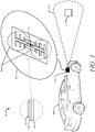
- FIG. 1 illustrates an example environment 100 in which a radar system 102 with a twin line fed dipole array 104 antenna 106 is used on a vehicle 108.
- the vehicle 108 may use the antenna 106 to enable operations of the radar system 102 that is configured to determine a proximity, an angle, or a velocity of one or more objects 110 in the proximity of the vehicle 108.
- the vehicle 108 can represent other types of motorized vehicles (e.g., a motorcycle, a bus, a tractor, a semi-trailer truck, or construction equipment), non-motorized vehicles (e.g., a bicycle), railed vehicles (e.g., a train or a trolley car), watercraft (e.g., a boat or a ship), aircraft (e.g., an airplane or a helicopter), or spacecraft (e.g., satellite).
- manufacturers can mount the radar system 102 to any moving platform, including moving machinery or robotic equipment.
- other devices e.g., desktop computers, tablets, laptops, televisions, computing watches, smartphones, gaming systems, and so forth
- the radar system 102 is mounted near, or integrated within, a front portion of the vehicle 108 to detect the object 110 and avoid collisions.
- the radar system 102 provides a field-of-view 112 towards the one or more objects 110.
- the radar system 102 can project the field-of-view 112 from any exterior surface of the vehicle 108.
- vehicle manufacturers can integrate the radar system 102 into a bumper, side mirror, headlights, rear lights, or any other interior or exterior location where the object 110 requires detection.
- the vehicle 108 includes multiple radar systems 102, such as a first radar system 102 and a second radar system 102 that provide a larger field-of-view 112.
- vehicle manufacturers can design the locations of the one or more radar systems 102 to provide a particular field-of-view 112 that encompasses a region of interest, including, for instance, in or around a travel lane aligned with a vehicle path.
- Example fields-of-view 112 include a 360-degree field-of-view, one or more 180-degree fields-of-view, one or more 90-degree fields-of-view, and so forth, which can overlap or be combined into a field-of-view 112 of a particular size.
- the described antenna 106 may include a plurality of dipoles 104 (e.g., the dipole array 104) that have a length (e.g., less than one-half wavelength of the operating frequency in free space) and position (e.g., approximately one-half wavelength of the operating frequency in free space from a neighboring dipole) that minimize cross-polarization, resulting in an improved signal strength in the azimuth plane.
- a radar system placed near the front of a vehicle can use the improved signal strength to focus on detecting objects immediately in front of the vehicle (e.g., in a travel lane aligned with a vehicle path).
- the improved signal strength of the antenna may provide increased accuracy when detecting the objects.
- the object 110 is composed of one or more materials that reflect radar signals. Depending on the application, the object 110 can represent a target of interest. In some cases, the object 110 can be a moving object or a stationary object.
- the stationary objects can be continuous (e.g., a concrete barrier, a guard rail) or discontinuous (e.g., a traffic cone) along a road portion.
- the radar system 102 emits electromagnetic radiation by transmitting one or more electromagnetic signals or waveforms via dipole arrays 104.
- the radar system 102 can detect and track the object 110 by transmitting and receiving one or more radar signals.
- the radar system 102 can transmit electromagnetic signals between 100 and 400 gigahertz (GHz), between 4 and 100 GHz, or between approximately 70 and 80 GHz.
- GHz gigahertz
- the radar system 102 can determine a distance to the object 110 based on the time it takes for the signals to travel from the radar system 102 to the object 110 and from the object 110 back to the radar system 102.
- the radar system 102 can also determine the location of the object 110 in terms of an angle based on the direction of a maximum amplitude echo signal received by the radar system 102.
- the radar system 102 can be part of the vehicle 108.
- the vehicle 108 can also include at least one automotive system that relies on data from the radar system 102, including a driver-assistance system, an autonomous-driving system, or a semi-autonomous-driving system.
- the radar system 102 can include an interface to the automotive systems.
- the radar system 102 can output, via the interface, a signal based on electromagnetic energy received by the radar system 102.
- the automotive systems of the vehicle 108 use radar data provided by the radar system 102 to perform a function.
- a driver-assistance system can provide blind-spot monitoring and generate an alert indicating a potential collision with the object 110 detected by the radar system 102.
- the radar data from the radar system 102 indicates when it is safe or unsafe to change lanes.
- An autonomous-driving system may move the vehicle 108 to a particular location on the road while avoiding collisions with the object 110 detected by the radar system 102.
- the radar data provided by the radar system 102 can provide information about a distance to and the location of the object 110 to enable the autonomous-driving system to perform emergency braking, perform a lane change, or adjust the speed of the vehicle 108.
- the radar system 102 generally includes a transmitter (not illustrated) and at least one antenna 106 to transmit electromagnetic signals.
- the radar system 102 generally includes a receiver (not illustrated) and at least one antenna 106 to receive reflected versions of these electromagnetic signals.
- the transmitter includes components for emitting electromagnetic signals.
- the receiver includes components to detect the reflected electromagnetic signals.
- the transmitter and the receiver can be incorporated together as a transceiver on the same integrated circuit (e.g., a transceiver integrated circuit) or separately on the same or different integrated circuits.
- the radar system 102 also includes one or more processors (not illustrated) and computer-readable storage media (CRM) (not illustrated).
- the processor can be a microprocessor or a system-on-chip.
- the processor executes instructions stored within the CRM As an example, the processor can control the operation of the transmitter.
- the processor can also process electromagnetic energy received by the antenna 106 and determine the location of the object 110 relative to the radar system 102.
- the processor can also generate radar data for the automotive systems. For example, the processor can control, based on processed electromagnetic energy from the antenna, an autonomous or semi-autonomous driving system of the vehicle 108.
- the antenna 106 can be defined as a first metal layer 114 of a PCB. Other layers of the PCB may include a substrate layer 116 and a second metal layer 118 that defines a conducting plane.
- a feed slot 114 may be positioned in and centered on the conductive plane and aligned with a lateral axis of the antenna.
- a microstrip or waveguide feed network can be coupled to the feed slot 114 and can electrically excite the antenna via the feed slot 114.
- each dipole in the dipole array 104 includes two dipole elements. The electromagnetic energy propagates through each arm of each branch of the antenna 106 and feeds each dipole element of the dipole differentially. In this manner, the antenna 106 is capable of radiating energy at a low cross-polarization level.
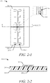
- FIG. 2-1 illustrates a top view 200-1 of a twin line fed dipole array antenna 200.
- the antenna 200 is an example of the antenna 106 of FIG. 1 .
- the antenna 200-1 includes an upper branch 202 and a lower branch 204.
- the upper branch 202 and the lower branch 204 each have two arms positioned orthogonally to a lateral axis 206. Said differently, the branches 202 and 204 are near perpendicular or normal to the lateral axis 206, which enables the antenna 200 to achieve a desired pattern.
- a feed slot 208-1 is centered on the lateral axis 206 and couples electromagnetic energy between the antenna 200 and a feed network or feed line.
- Each arm can have one or more dipole elements (e.g., dipole elements 210-1 and 210-2 of dipole 210). Each dipole 210 is sized and positioned to allow for optimal electromagnetic energy transfer.
- FIG. 2-2 illustrates a cross-section view 200-2 of the twin line fed dipole array antenna 200.
- the antenna 200 is illustrated as a PCB in this example.
- a first metal layer 212 may be the layer on which the antenna 200 structure is located.
- a substrate layer 214 may separate the first metal layer 212 from a second metal layer 216 that defines a conducting plane.
- the second metal layer 216 includes a feed slot 208-2 that is positioned in and centered on the conducting plane to align with a lateral axis (e.g., the lateral axis 206).
- the feed slot 208-2 may be electrically excited by various methods, including the non-limiting examples of a microstrip line couple, a waveguide end, a waveguide, or a substrate integrated waveguide (SIW).
- the method of exciting the slot may define the type of feed line for the antenna.
- FIG. 3 illustrates different shapes a dipole element may have on a twin line fed dipole array antenna 300.
- the antenna 300 is another example of the antenna 106 of FIG. 1 .
- Each arm 304 of each branch of the antenna 300 includes three dipole elements 302.
- each arm 304 of each branch of the antenna 300 may include a greater or lesser quantity of dipole elements, depending on the size constraints of the antenna 300, and/or depending on the desired antenna pattern.
- the antenna 300 is illustrated with the dipole elements 302 positioned approximately orthogonal to each respective arm 304 and having an approximately rectangular shape 302-1.
- the dipole elements 302 may have other shapes, including a bowtie shape 302-2, a circular shape 302-3, an oval shape 302-4, a C-shape 302-5, or an L-shape 302-6.
- the shape of the dipole elements 302 may depend on different factors such as the particular application or the specifics of the system (e.g., the radar system 102) with which the antenna 300 is coupled.
- Each branch of the antenna 300 may be symmetrical with respect to a lateral axis (e.g., the lateral axis 206 from FIG. 2-1 ). That is, the upper branch and the lower branch (e.g., the upper branch 202 and the lower branch 204 from FIG. 2-1 ) may mirror each other along the lateral axis.
- FIGs. 4 through 7 illustrate example feeding methods for a twin line fed dipole array antenna. The method used depends on the configuration of the feed network or how the lines connecting the transceiver module to the antenna are routed. Other feeding methods that are not illustrated may, likewise, be used with the twin line fed dipole array antenna.
- FIG. 4 illustrates an example implementation of a twin line fed dipole array antenna 400 coupled to a waveguide 402 with an end feed. Two views, a rear view 400-1 and a rear perspective view 400-2 of the antenna 400, are illustrated in FIG. 4 for orientation.
- the waveguide 402 is coupled to a feed slot 404 (e.g., the feed slot 114, 208) on an end opposite of the waveguide input 406.
- the coupling can be made via contact, which can be strengthened using electrical coupling means (e.g., solder connection, male-female connectors).
- FIG. 5 illustrates an example implementation of a twin line fed dipole array antenna 500 coupled to a waveguide 502 with an E-plane feed.
- View 500-1 is a rear view
- view 500-2 is a rear perspective view.
- the waveguide 502 is coupled to a feed slot 504 on the E-plane of the waveguide.
- a waveguide input 506 is positioned on an end of the waveguide 502 that is longitudinal to the antenna and adjacent to the E-plane feed.
- FIG. 6 illustrates an example implementation of a twin line fed dipole array antenna 600 coupled to a waveguide 602 with an H-plane feed.
- the antenna is coupled to an H-plane waveguide via a feed slot 604.
- a waveguide input 606 is positioned on an end of the waveguide 602 that is longitudinal to the antenna and adjacent to the H-plane feed.
- FIG. 7 illustrates an example implementation of a twin line fed dipole array antenna 700 coupled to a microstrip 702 line feed. Similar to FIGs. 4 - 6 , FIG. 7 includes a rear view 700-1 and a rear perspective view 700-2 for orientation.
- the microstrip 702 is coupled to a feed slot 704 by a feed line (not illustrated).
- the microstrip 702 extends laterally away from the feed slot 704.
- a microstrip input 706 is located on the lateral extension of the microstrip 702.
- FIG. 8 illustrates an example method 800 that can be used for manufacturing a twin line fed dipole array antenna following techniques, apparatuses, and systems of this disclosure.
- Method 800 is shown as sets of operations (or acts) performed, but not necessarily limited to the order or combinations in which the operations are shown herein. Further, any of one or more of the operations may be repeated, combined, or reorganized to provide other methods.
- reference may be made to the environment 100 of FIG. 1 and entities detailed in FIGs. 1 through 7 , reference to which is made for example only.
- the techniques are not limited to performance by one entity or multiple entities.
- a twin line fed dipole array antenna is formed.
- the antenna 106, 200, 300, 400, 500, 600, and/or 700 can be stamped, etched, cut, machined, cast, molded, or formed in some other way.
- the antenna is integrated into a system.
- the antenna 106, 200, 300, 400, 500, 600, and/or 700 is electrically coupled to a feed line or feed network that may include one or more of different types of components, including different types of waveguides or microstrip.
- electromagnetic signals are received or transmitted via the antenna at or by the system, respectively.
- the antenna 106 receives or transmits signals routed through the radar system 102.
- a twin line fed dipole array antenna is formed as an outer layer of a PCB.
- Other layers of the PCB include an inner substrate layer and a conducting plane layer on the side of the inner substrate layer opposite of the antenna layer.
- the conducting plane layer includes a feed slot positioned such that a lateral axis of the antenna layer is centered on it.
- the antenna has an upper branch and a lower branch that mirror each other along a lateral axis.
- Each branch includes two arms parallel to each other and extending orthogonally from the lateral axis.
- the two parallel arms of each branch include a plurality of dipoles with the dipole elements of each of the plurality of dipoles extending orthogonally from the two parallel arms of each branch.
- the twin line fed dipole array antenna is part of a radar system integrated in an autonomous vehicle.
- the radar system assists the self-driving of the autonomous vehicle by identifying and tracking objects in the vicinity of the autonomous vehicle. Accuracy in tracking the objects is critical to avoiding collisions.
- the antenna positioned at the front of the autonomous vehicle, is coupled to the radar system through a feed network that includes a waveguide with an end feed. Electromagnetic signals, transmitted by the antenna, reflected off an object, and then received by the antenna, enable the radar system to track the object.
- the autonomous vehicle is able to avoid a collision with the object due to the accuracy provided by the antenna system.
- a second example has the same type of twin line fed dipole array antenna as the first example, and is, likewise, mounted in an autonomous vehicle as part of a radar system.
- the feed network between the antenna and the radar system includes a microstrip line. Due to the versatility provided by the centrally positioned feed slot.
- the antenna is capable of being coupled to the microstrip.
- Other similar examples may include the antenna being coupled to the feed network through other types of waveguides or connections.
- a twin line fed dipole array antenna may increase the accuracy of the system to which it is coupled by reducing the cross-polarization levels. Due to the feed slot being centrally positioned with respect to the antenna (e.g., centered on a lateral axis of the antenna), the antenna may be coupled to different types of feed networks in a manner that minimizes a form factor of a housing of the antenna and feed network. This makes the twin line fed dipole array antenna a desirable candidate for automotive radar system applications.
- Example 1 An apparatus comprising: a twin line fed dipole array antenna, the antenna comprising: a first metal layer defining a transmission line configured to receive electromagnetic energy as input, the transmission line having a lateral axis and at least: a first branch comprising a first arm and a second arm parallel to the first arm, each of the first arm and the second arm being orthogonal to and positioned on a first side of the lateral axis; and a second branch comprising a third arm and a fourth arm parallel to the third arm, each of the third arm and the fourth arm being orthogonal to and positioned on a second side of the lateral axis that is opposite the first side of the lateral axis.
- Example 2 The apparatus of Example 1, the apparatus further comprising: a second metal layer defining a conductive plane; and a substrate layer having two sides of the substrate layer, the first metal layer positioned adjacent to a first side of the substrate layer and the second metal layer positioned adjacent to a second side of the substrate layer.
- Example 3 The apparatus of any one of the preceding Examples, wherein the first metal layer, the second metal layer, and the substrate layer are layers of a printed circuit board.
- Example 4 The apparatus of any one of the preceding Examples, the apparatus further comprising: a feed slot positioned in and centered on the conductive plane to align with the lateral axis, the feed slot configured to excite the transmission line.
- Example 5 The apparatus of any one of the preceding Examples, wherein the feed slot is excited by a microstrip line, a waveguide end, a waveguide, or a substrate integrated waveguide.
- Example 6 The apparatus of any one of the preceding Examples, wherein: the first branch further comprises a first pair of dipole elements, a first dipole element of the first pair of dipole elements positioned at an end of and generally orthogonal to the first arm of the first branch, and a second dipole element of the first pair of dipole elements positioned at an end of and generally orthogonal to the second arm of the first branch.
- Example 7 The apparatus of any one of the preceding Examples, wherein: the second branch further comprises a second pair of dipole elements, a first dipole element of the second pair of dipole elements positioned at an end of and generally orthogonal to the third arm of the second branch, and a second dipole element of the second pair of dipole elements positioned at an end of and generally orthogonal to the fourth arm of the second branch.
- Example 8 The apparatus of any one of the preceding Examples, wherein: the first branch further comprises a plurality of pairs of dipole elements, each pair of dipole elements on the first branch separated from another pair of dipole elements on the first branch by approximately one-half of a wavelength of an operating frequency of the antenna.
- Example 9 The apparatus of any one of the preceding Examples, wherein: the second branch further comprises a plurality of pairs of dipole elements, each pair of dipole elements on the second branch separated from another pair of dipole elements on the second branch by approximately one-half of the wavelength of the operating frequency of the antenna.
- Example 10 The apparatus of any one of the preceding Examples, wherein: each dipole element of the plurality of pairs of dipole elements extends generally orthogonal to the arms and has an approximately rectangular shape, bowtie shape, circular shape, oval shape, C shape, or L shape.
- Example 11 A system comprising: a twin line fed dipole array antenna according to the apparatus any one of the preceding examples; and a device configured to transmit or receive electromagnetic signals via the antenna.
- Example 12 The system of any one of the preceding Examples, the system further comprising: a second metal layer defining a conductive plane; and a substrate layer having two sides of the substrate layer, the first metal layer positioned adjacent to a first side of the substrate layer and the second metal layer positioned adjacent to a second side of the substrate layer.
- Example 13 The system of any one of the preceding Examples, wherein: the first branch further comprises a first pair of dipole elements, a first dipole element of the first pair of dipole elements positioned at an end of and generally orthogonal to the first arm of the first branch, and a second dipole element of the first pair of dipole elements positioned at an end of and generally orthogonal to the second arm of the first branch.
- Example 14 The system of any one of the preceding Examples, wherein: the second branch further comprises a second pair of dipole elements, a first dipole element of the second pair of dipole elements positioned at an end of and generally orthogonal to the third arm of the second branch, and a second dipole element of the second pair of dipole elements positioned at an end of and generally orthogonal to the fourth arm of the second branch.
- Example 15 The system of any one of the preceding Examples, wherein: the first branch further comprises a plurality of pairs of dipole elements, each pair of dipole elements on the first branch separated from another pair of dipole elements on the first branch by approximately one-half of a wavelength of an operating frequency of the antenna.
- Example 16 The system of any one of the preceding Examples, wherein: the second branch further comprises a plurality of pairs of dipole elements, each pair of dipole elements on the second branch separated from another pair of dipole elements on the second branch by approximately one-half of a wavelength of an operating frequency of the antenna.
- Example 17 The system of any one of the preceding Examples, wherein the system is a vehicle, the device is a radar system, and the apparatus includes a waveguide with an end feed.
- Example 18 The system of any one of the preceding Examples, wherein the system is a vehicle, the device is a radar system, and the apparatus includes an E-plane waveguide.
- Example 19 The system of any one of the preceding Examples, wherein the system is a vehicle, the device is a radar system, and the apparatus includes an H-plane waveguide.
- Example 20 The system of any one of the preceding Examples, wherein the system is a vehicle, the device is a radar system, and the apparatus includes a microstrip line.
Landscapes
- Engineering & Computer Science (AREA)
- Radar, Positioning & Navigation (AREA)
- Remote Sensing (AREA)
- Computer Security & Cryptography (AREA)
- Variable-Direction Aerials And Aerial Arrays (AREA)
Applications Claiming Priority (3)
| Application Number | Priority Date | Filing Date | Title |
|---|---|---|---|
| US202063127873P | 2020-12-18 | 2020-12-18 | |
| US202163169093P | 2021-03-31 | 2021-03-31 | |
| US17/234,337 US11502420B2 (en) | 2020-12-18 | 2021-04-19 | Twin line fed dipole array antenna |
Publications (1)
| Publication Number | Publication Date |
|---|---|
| EP4016740A1 true EP4016740A1 (de) | 2022-06-22 |
Family
ID=78819435
Family Applications (1)
| Application Number | Title | Priority Date | Filing Date |
|---|---|---|---|
| EP21211478.9A Pending EP4016740A1 (de) | 2020-12-18 | 2021-11-30 | Durch doppelleitung gespeiste dipolgruppenantenne |
Country Status (3)
| Country | Link |
|---|---|
| US (1) | US11502420B2 (de) |
| EP (1) | EP4016740A1 (de) |
| CN (1) | CN114649671A (de) |
Citations (4)
| Publication number | Priority date | Publication date | Assignee | Title |
|---|---|---|---|---|
| CN102157787A (zh) * | 2010-12-22 | 2011-08-17 | 中国科学院上海微系统与信息技术研究所 | 用于双波束交通信息检测雷达的平面阵列微波天线 |
| CN109980361A (zh) * | 2019-04-08 | 2019-07-05 | 深圳市华讯方舟微电子科技有限公司 | 阵列天线 |
| US20190245276A1 (en) * | 2018-02-06 | 2019-08-08 | Delphi Technologies, Llc | Wide angle coverage antenna with parasitic elements |
| DE112017006415T5 (de) * | 2016-12-21 | 2019-09-05 | Mitsubishi Electric Corporation | Wellenleiter-mikrostreifenleiter-wandler |
Family Cites Families (87)
| Publication number | Priority date | Publication date | Assignee | Title |
|---|---|---|---|---|
| US3462713A (en) | 1967-07-19 | 1969-08-19 | Bell Telephone Labor Inc | Waveguide-stripline transducer |
| US3579149A (en) | 1969-12-08 | 1971-05-18 | Westinghouse Electric Corp | Waveguide to stripline transition means |
| NL7609903A (nl) | 1976-09-07 | 1978-03-09 | Philips Nv | Microgolfinrichting voor het omzetten van een golfpijp- in een microstripgeleiderstructuur. |
| US4453142A (en) | 1981-11-02 | 1984-06-05 | Motorola Inc. | Microstrip to waveguide transition |
| US4562416A (en) | 1984-05-31 | 1985-12-31 | Sanders Associates, Inc. | Transition from stripline to waveguide |
| US4590480A (en) | 1984-08-31 | 1986-05-20 | Rca Corporation | Broadcast antenna which radiates horizontal polarization towards distant locations and circular polarization towards nearby locations |
| IL82331A (en) * | 1987-04-26 | 1991-04-15 | M W A Ltd | Microstrip and stripline antenna |
| US5986527A (en) | 1995-03-28 | 1999-11-16 | Murata Manufacturing Co., Ltd. | Planar dielectric line and integrated circuit using the same line |
| JP3366552B2 (ja) | 1997-04-22 | 2003-01-14 | 京セラ株式会社 | 誘電体導波管線路およびそれを具備する多層配線基板 |
| SE521407C2 (sv) * | 1997-04-30 | 2003-10-28 | Ericsson Telefon Ab L M | Mikrovägantennsystem med en plan konstruktion |
| CA2292064C (en) | 1998-12-25 | 2003-08-19 | Murata Manufacturing Co., Ltd. | Line transition device between dielectric waveguide and waveguide, and oscillator and transmitter using the same |
| US6590477B1 (en) | 1999-10-29 | 2003-07-08 | Fci Americas Technology, Inc. | Waveguides and backplane systems with at least one mode suppression gap |
| ATE264550T1 (de) | 2000-10-18 | 2004-04-15 | Nokia Corp | Hohlleiter-streifenleiter-übergang |
| EP1346431A1 (de) | 2000-12-21 | 2003-09-24 | Paratek Microwave, Inc. | Hohlleiter-mikrostreifenleiterübergang |
| US6967347B2 (en) | 2001-05-21 | 2005-11-22 | The Regents Of The University Of Colorado | Terahertz interconnect system and applications |
| JP2003289201A (ja) | 2002-03-28 | 2003-10-10 | Anritsu Corp | ポスト壁導波管と空洞導波管の接続変換構造 |
| EP1628360B1 (de) * | 2004-08-21 | 2007-10-10 | Samsung Electronics Co., Ltd | Kleine gleichrichtende Antenne |
| US7098070B2 (en) | 2004-11-16 | 2006-08-29 | International Business Machines Corporation | Device and method for fabricating double-sided SOI wafer scale package with through via connections |
| CN2796131Y (zh) | 2005-05-30 | 2006-07-12 | 东南大学 | 多层基片集成波导椭圆响应滤波器 |
| EP2009731B1 (de) | 2006-03-31 | 2014-01-01 | Kyocera Corporation | Dielektrische welllenleiteranordnung, phasenschieber, hochfrequenzschalter und mit dielektrischer wellenleiteranordnung ausgestattetes dämpfungsglied, hochfrequenzsender, hochfrequenzempfänger, hochfrequenzsender/empfänger, radaranordnung, array-antenne, und verfahren zur herstellung eines dielektrische wellenleiteranordnung |
| CN101467082B (zh) | 2006-06-12 | 2011-12-14 | 加利福尼亚太平洋生物科学公司 | 实施分析反应的基材 |
| KR100846872B1 (ko) | 2006-11-17 | 2008-07-16 | 한국전자통신연구원 | 유전체 도파관 대 전송선의 밀리미터파 천이 장치 |
| JP4365852B2 (ja) | 2006-11-30 | 2009-11-18 | 株式会社日立製作所 | 導波管構造 |
| EP1936741A1 (de) | 2006-12-22 | 2008-06-25 | Sony Deutschland GmbH | Flexible substratintegrierte Wellenleiter |
| US8231284B2 (en) | 2007-03-26 | 2012-07-31 | International Business Machines Corporation | Ultra-high bandwidth, multiple-channel full-duplex, single-chip CMOS optical transceiver |
| US7768457B2 (en) | 2007-06-22 | 2010-08-03 | Vubiq, Inc. | Integrated antenna and chip package and method of manufacturing thereof |
| JP5179513B2 (ja) | 2007-12-28 | 2013-04-10 | 京セラ株式会社 | 高周波伝送線路の接続構造、配線基板、高周波モジュールおよびレーダ装置 |
| CA2629035A1 (en) | 2008-03-27 | 2009-09-27 | Her Majesty The Queen In Right Of Canada, As Represented By The Minister Of Industry, Through The Communications Research Centre Canada | Waveguide filter with broad stopband based on sugstrate integrated waveguide scheme |
| JP5172481B2 (ja) | 2008-06-05 | 2013-03-27 | 株式会社東芝 | ポスト壁導波路によるショートスロット方向性結合器とこれを用いたバトラーマトリクス及び車載レーダアンテナ |
| US8089327B2 (en) | 2009-03-09 | 2012-01-03 | Toyota Motor Engineering & Manufacturing North America, Inc. | Waveguide to plural microstrip transition |
| JP5309209B2 (ja) | 2009-03-31 | 2013-10-09 | 京セラ株式会社 | 導波構造体、ならびに、導波構造体を含む高周波モジュールおよびレーダ装置 |
| CN201383535Y (zh) | 2009-04-01 | 2010-01-13 | 惠州市硕贝德通讯科技有限公司 | 一种矩形波导-基片集成波导信号转换及功率分配器 |
| JP5443594B2 (ja) | 2009-05-08 | 2014-03-19 | テレフオンアクチーボラゲット エル エム エリクソン(パブル) | チップから導波管ポートへの変換器 |
| FR2953651B1 (fr) | 2009-12-07 | 2012-01-20 | Eads Defence & Security Sys | Dispositif de transition hyperfrequence entre une ligne a micro-ruban et un guide d'onde rectangulaire |
| US9774076B2 (en) | 2010-08-31 | 2017-09-26 | Siklu Communication ltd. | Compact millimeter-wave radio systems and methods |
| US8674885B2 (en) | 2010-08-31 | 2014-03-18 | Siklu Communication ltd. | Systems for interfacing waveguide antenna feeds with printed circuit boards |
| KR101761920B1 (ko) | 2011-02-16 | 2017-07-26 | 삼성전기주식회사 | 유전체 도파관 안테나 |
| EP2500978B1 (de) | 2011-03-17 | 2013-07-10 | Sivers Ima AB | Wellenleiterübergang |
| GB2489950A (en) | 2011-04-12 | 2012-10-17 | Filtronic Plc | A substrate integrated waveguide (SIW) to air filled waveguide transition comprising a tapered dielectric layer |
| US9147924B2 (en) | 2011-09-02 | 2015-09-29 | The United States Of America As Represented By The Secretary Of The Army | Waveguide to co-planar-waveguide (CPW) transition |
| CN102420352A (zh) | 2011-12-14 | 2012-04-18 | 佛山市健博通电讯实业有限公司 | 一种双极化天线 |
| JP2013187752A (ja) | 2012-03-08 | 2013-09-19 | Mitsubishi Electric Corp | 導波管スロットアレーアンテナ装置 |
| EP2862230B1 (de) | 2012-06-18 | 2016-08-10 | Huawei Technologies Co., Ltd. | Hohlleiterstruktur mit richtkoppler und verfahren |
| JP5694246B2 (ja) | 2012-07-13 | 2015-04-01 | 株式会社東芝 | 導波管接続構造、アンテナ装置およびレーダ装置 |
| US20140106684A1 (en) | 2012-10-15 | 2014-04-17 | Qualcomm Mems Technologies, Inc. | Transparent antennas on a display device |
| JP2016503245A (ja) | 2013-01-10 | 2016-02-01 | 日本電気株式会社 | 平面伝送線路および導波管の間の広帯域変換器 |
| CN105190990B (zh) | 2013-03-24 | 2018-01-26 | 瑞典爱立信有限公司 | 在siw和波导接口之间的过渡 |
| CN103515682B (zh) | 2013-07-24 | 2015-07-29 | 中国电子科技集团公司第五十五研究所 | 多层阶梯式基片集成波导实现微带至波导的垂直过渡结构 |
| CN103650243B (zh) | 2013-07-31 | 2016-03-30 | 华为技术有限公司 | 一种天线 |
| EP2843758A1 (de) | 2013-08-27 | 2015-03-04 | Microelectronics Technology Inc. | Mehrlagige Leiterplatte mit Wellenleiter zu einer Mikrostreifen-Übergangsstruktur |
| US10014566B2 (en) | 2013-10-01 | 2018-07-03 | Sony Semiconductor Solutions Corporation | Connector apparatus and communication system |
| US9059490B2 (en) | 2013-10-08 | 2015-06-16 | Blackberry Limited | 60 GHz integrated circuit to printed circuit board transitions |
| JP6269127B2 (ja) | 2014-02-07 | 2018-01-31 | 富士通株式会社 | 高周波モジュール及びその製造方法 |
| JP5727069B1 (ja) | 2014-04-23 | 2015-06-03 | 株式会社フジクラ | 導波路型スロットアレイアンテナ及びスロットアレイアンテナモジュール |
| US9620841B2 (en) | 2014-06-13 | 2017-04-11 | Nxp Usa, Inc. | Radio frequency coupling structure |
| US10103447B2 (en) | 2014-06-13 | 2018-10-16 | Nxp Usa, Inc. | Integrated circuit package with radio frequency coupling structure |
| US9583811B2 (en) | 2014-08-07 | 2017-02-28 | Infineon Technologies Ag | Transition between a plastic waveguide and a semiconductor chip, where the semiconductor chip is embedded and encapsulated within a mold compound |
| KR101621480B1 (ko) | 2014-10-16 | 2016-05-16 | 현대모비스 주식회사 | 도파관 대 유전체 도파관의 천이 구조 |
| US9666930B2 (en) | 2014-10-23 | 2017-05-30 | Nxp Usa, Inc. | Interface between a semiconductor die and a waveguide, where the interface is covered by a molding compound |
| WO2016092084A1 (en) | 2014-12-12 | 2016-06-16 | Sony Corporation | Microwave antenna apparatus, packing and manufacturing method |
| US9537199B2 (en) | 2015-03-19 | 2017-01-03 | International Business Machines Corporation | Package structure having an integrated waveguide configured to communicate between first and second integrated circuit chips |
| US10109604B2 (en) | 2015-03-30 | 2018-10-23 | Sony Corporation | Package with embedded electronic components and a waveguide cavity through the package cover, antenna apparatus including package, and method of manufacturing the same |
| KR101689353B1 (ko) | 2015-04-13 | 2016-12-23 | 성균관대학교산학협력단 | 실리콘 밀리미터파 칩용 칩상 도파관 급전기 및 급전 방법 및, 이를 이용한 다중 입출력 밀리미터파 송수신 장치 |
| CN104900956A (zh) | 2015-05-06 | 2015-09-09 | 东南大学 | 一种波导到基片集成波导的转换装置 |
| CN104993254B (zh) * | 2015-07-15 | 2018-01-16 | 华南理工大学 | 一种宽带方向图可重构天线 |
| US10083923B2 (en) | 2015-09-21 | 2018-09-25 | Intel Corporation | Platform with thermally stable wireless interconnects |
| CN105680133B (zh) | 2016-01-11 | 2018-08-10 | 中国电子科技集团公司第十研究所 | 基片集成脊波导板间垂直互联电路结构 |
| US20190013563A1 (en) | 2016-01-20 | 2019-01-10 | Sony Corporation | Connector module, communication circuit board, and electronic device |
| CN105609909A (zh) | 2016-03-08 | 2016-05-25 | 电子科技大学 | 一种用于Ka波段矩形波导转基片集成波导的装置 |
| WO2018003932A1 (en) | 2016-06-29 | 2018-01-04 | Nidec Elesys Corporation | Waveguide device module and microwave module |
| CN105958167B (zh) | 2016-07-01 | 2019-03-05 | 北京交通大学 | 垂直基片集成波导及包括该波导的垂直连接结构 |
| KR101963936B1 (ko) | 2016-11-08 | 2019-07-31 | 한국과학기술원 | 전자파 신호 송수신 안테나 및 em-터널이 내장된 구조를 갖는 인쇄회로기판 및 그 제작 방법 |
| US9935065B1 (en) | 2016-12-21 | 2018-04-03 | Infineon Technologies Ag | Radio frequency device packages and methods of formation thereof |
| US10468736B2 (en) | 2017-02-08 | 2019-11-05 | Aptiv Technologies Limited | Radar assembly with ultra wide band waveguide to substrate integrated waveguide transition |
| EP3364457A1 (de) | 2017-02-15 | 2018-08-22 | Nxp B.V. | Integriertes schaltungsgehäuse mit antenne |
| US10317459B2 (en) | 2017-04-03 | 2019-06-11 | Nvidia Corporation | Multi-chip package with selection logic and debug ports for testing inter-chip communications |
| JP2018182740A (ja) | 2017-04-13 | 2018-11-15 | 日本電産株式会社 | スロットアレーアンテナ |
| DE102017111319A1 (de) | 2017-05-24 | 2018-11-29 | Miele & Cie. Kg | Einrichtung zur Erzeugung und Transmission von Hochfrequenzwellen (HF-Wellen) |
| CN108987866A (zh) | 2017-06-05 | 2018-12-11 | 日本电产株式会社 | 波导装置以及具有该波导装置的天线装置 |
| DE102018115610A1 (de) | 2017-06-30 | 2019-01-03 | Nidec Corporation | Wellenleitervorrichtungsmodul, Mikrowellenmodul, Radarvorrichtung und Radarsystem |
| US11183751B2 (en) | 2017-09-20 | 2021-11-23 | Aptiv Technologies Limited | Antenna device with direct differential input useable on an automated vehicle |
| US10283832B1 (en) * | 2017-12-26 | 2019-05-07 | Vayyar Imaging Ltd. | Cavity backed slot antenna with in-cavity resonators |
| CN207868388U (zh) * | 2018-02-13 | 2018-09-14 | 中磊电子(苏州)有限公司 | 天线系统 |
| DE102019200893B4 (de) | 2019-01-21 | 2023-06-15 | Infineon Technologies Ag | Verfahren zum Erzeugen eines Hohlleiters, Schaltungsvorrichtung und Radarsystem |
| CN209389219U (zh) | 2019-02-25 | 2019-09-13 | 贵州航天电子科技有限公司 | 一种适用于增材制造的波导缝隙阵列天线结构 |
| US10775573B1 (en) | 2019-04-03 | 2020-09-15 | International Business Machines Corporation | Embedding mirror with metal particle coating |
| US11527808B2 (en) | 2019-04-29 | 2022-12-13 | Aptiv Technologies Limited | Waveguide launcher |
-
2021
- 2021-04-19 US US17/234,337 patent/US11502420B2/en active Active
- 2021-11-30 EP EP21211478.9A patent/EP4016740A1/de active Pending
- 2021-12-20 CN CN202111563233.9A patent/CN114649671A/zh active Pending
Patent Citations (4)
| Publication number | Priority date | Publication date | Assignee | Title |
|---|---|---|---|---|
| CN102157787A (zh) * | 2010-12-22 | 2011-08-17 | 中国科学院上海微系统与信息技术研究所 | 用于双波束交通信息检测雷达的平面阵列微波天线 |
| DE112017006415T5 (de) * | 2016-12-21 | 2019-09-05 | Mitsubishi Electric Corporation | Wellenleiter-mikrostreifenleiter-wandler |
| US20190245276A1 (en) * | 2018-02-06 | 2019-08-08 | Delphi Technologies, Llc | Wide angle coverage antenna with parasitic elements |
| CN109980361A (zh) * | 2019-04-08 | 2019-07-05 | 深圳市华讯方舟微电子科技有限公司 | 阵列天线 |
Also Published As
| Publication number | Publication date |
|---|---|
| CN114649671A (zh) | 2022-06-21 |
| US11502420B2 (en) | 2022-11-15 |
| US20220200163A1 (en) | 2022-06-23 |
Similar Documents
| Publication | Publication Date | Title |
|---|---|---|
| US11644533B2 (en) | Multiple polarization radar unit | |
| US11223112B2 (en) | Inverted microstrip travelling wave patch array antenna system | |
| US11515624B2 (en) | Integrated cavity backed slot array antenna system | |
| US20230327330A1 (en) | Waveguide with Radiation Slots and Parasitic Elements for Asymmetrical Coverage | |
| EP4016732A1 (de) | Wellenleiter mit schlitzgespeisten dipolelementen | |
| EP4016740A1 (de) | Durch doppelleitung gespeiste dipolgruppenantenne | |
| EP4099500A1 (de) | Wellenförmige grundruktur für gruppenantennen | |
| US11588228B2 (en) | Exposed portion of a printed circuit board (PCB) configured to provide isolation among radar antennas | |
| US11977146B2 (en) | Radar device and detection method of target position of radar device | |
| EP4040595A1 (de) | Geformte wellenleiterantennen einer radaranordnung | |
| CN215894947U (zh) | 车载雷达传感器 | |
| US11901601B2 (en) | Waveguide with a zigzag for suppressing grating lobes | |
| EP4283777A1 (de) | Vertikaler mikrostreifen-wellenleiter-übergang | |
| EP4167688A1 (de) | Antennen-leiterplattenübergang | |
| US20230352845A1 (en) | Waveguide with Slot Antennas and Reflectors | |
| US11721905B2 (en) | Waveguide with a beam-forming feature with radiation slots | |
| CN113571892B (zh) | 一种天线装置、车载毫米波雷达及汽车 | |
| CN117117483A (zh) | 天线结构、毫米波雷达及可移动设备 | |
| CN116995390A (zh) | 具有槽天线和反射器的波导 |
Legal Events
| Date | Code | Title | Description |
|---|---|---|---|
| PUAI | Public reference made under article 153(3) epc to a published international application that has entered the european phase |
Free format text: ORIGINAL CODE: 0009012 |
|
| STAA | Information on the status of an ep patent application or granted ep patent |
Free format text: STATUS: THE APPLICATION HAS BEEN PUBLISHED |
|
| AK | Designated contracting states |
Kind code of ref document: A1 Designated state(s): AL AT BE BG CH CY CZ DE DK EE ES FI FR GB GR HR HU IE IS IT LI LT LU LV MC MK MT NL NO PL PT RO RS SE SI SK SM TR |
|
| STAA | Information on the status of an ep patent application or granted ep patent |
Free format text: STATUS: REQUEST FOR EXAMINATION WAS MADE |
|
| 17P | Request for examination filed |
Effective date: 20221208 |
|
| RBV | Designated contracting states (corrected) |
Designated state(s): AL AT BE BG CH CY CZ DE DK EE ES FI FR GB GR HR HU IE IS IT LI LT LU LV MC MK MT NL NO PL PT RO RS SE SI SK SM TR |
|
| GRAP | Despatch of communication of intention to grant a patent |
Free format text: ORIGINAL CODE: EPIDOSNIGR1 |
|
| STAA | Information on the status of an ep patent application or granted ep patent |
Free format text: STATUS: GRANT OF PATENT IS INTENDED |
|
| INTG | Intention to grant announced |
Effective date: 20240328 |
|
| RAP1 | Party data changed (applicant data changed or rights of an application transferred) |
Owner name: APTIV TECHNOLOGIES AG |