EP4016739A1 - Waveguide with squint alteration - Google Patents
Waveguide with squint alteration Download PDFInfo
- Publication number
- EP4016739A1 EP4016739A1 EP21211452.4A EP21211452A EP4016739A1 EP 4016739 A1 EP4016739 A1 EP 4016739A1 EP 21211452 A EP21211452 A EP 21211452A EP 4016739 A1 EP4016739 A1 EP 4016739A1
- Authority
- EP
- European Patent Office
- Prior art keywords
- waveguide
- linear portion
- divider
- opening
- electromagnetic
- Prior art date
- Legal status (The legal status is an assumption and is not a legal conclusion. Google has not performed a legal analysis and makes no representation as to the accuracy of the status listed.)
- Granted
Links
Images




Classifications
-
- H—ELECTRICITY
- H01—ELECTRIC ELEMENTS
- H01Q—ANTENNAS, i.e. RADIO AERIALS
- H01Q21/00—Antenna arrays or systems
- H01Q21/0006—Particular feeding systems
- H01Q21/0037—Particular feeding systems linear waveguide fed arrays
- H01Q21/0043—Slotted waveguides
- H01Q21/005—Slotted waveguides arrays
-
- G—PHYSICS
- G01—MEASURING; TESTING
- G01S—RADIO DIRECTION-FINDING; RADIO NAVIGATION; DETERMINING DISTANCE OR VELOCITY BY USE OF RADIO WAVES; LOCATING OR PRESENCE-DETECTING BY USE OF THE REFLECTION OR RERADIATION OF RADIO WAVES; ANALOGOUS ARRANGEMENTS USING OTHER WAVES
- G01S7/00—Details of systems according to groups G01S13/00, G01S15/00, G01S17/00
- G01S7/02—Details of systems according to groups G01S13/00, G01S15/00, G01S17/00 of systems according to group G01S13/00
- G01S7/28—Details of pulse systems
- G01S7/2813—Means providing a modification of the radiation pattern for cancelling noise, clutter or interfering signals, e.g. side lobe suppression, side lobe blanking, null-steering arrays
-
- H—ELECTRICITY
- H01—ELECTRIC ELEMENTS
- H01P—WAVEGUIDES; RESONATORS, LINES, OR OTHER DEVICES OF THE WAVEGUIDE TYPE
- H01P3/00—Waveguides; Transmission lines of the waveguide type
-
- G—PHYSICS
- G01—MEASURING; TESTING
- G01S—RADIO DIRECTION-FINDING; RADIO NAVIGATION; DETERMINING DISTANCE OR VELOCITY BY USE OF RADIO WAVES; LOCATING OR PRESENCE-DETECTING BY USE OF THE REFLECTION OR RERADIATION OF RADIO WAVES; ANALOGOUS ARRANGEMENTS USING OTHER WAVES
- G01S7/00—Details of systems according to groups G01S13/00, G01S15/00, G01S17/00
- G01S7/02—Details of systems according to groups G01S13/00, G01S15/00, G01S17/00 of systems according to group G01S13/00
- G01S7/40—Means for monitoring or calibrating
- G01S7/4004—Means for monitoring or calibrating of parts of a radar system
- G01S7/4026—Antenna boresight
-
- H—ELECTRICITY
- H01—ELECTRIC ELEMENTS
- H01Q—ANTENNAS, i.e. RADIO AERIALS
- H01Q1/00—Details of, or arrangements associated with, antennas
- H01Q1/27—Adaptation for use in or on movable bodies
- H01Q1/32—Adaptation for use in or on road or rail vehicles
- H01Q1/3208—Adaptation for use in or on road or rail vehicles characterised by the application wherein the antenna is used
- H01Q1/3233—Adaptation for use in or on road or rail vehicles characterised by the application wherein the antenna is used particular used as part of a sensor or in a security system, e.g. for automotive radar, navigation systems
-
- G—PHYSICS
- G01—MEASURING; TESTING
- G01S—RADIO DIRECTION-FINDING; RADIO NAVIGATION; DETERMINING DISTANCE OR VELOCITY BY USE OF RADIO WAVES; LOCATING OR PRESENCE-DETECTING BY USE OF THE REFLECTION OR RERADIATION OF RADIO WAVES; ANALOGOUS ARRANGEMENTS USING OTHER WAVES
- G01S13/00—Systems using the reflection or reradiation of radio waves, e.g. radar systems; Analogous systems using reflection or reradiation of waves whose nature or wavelength is irrelevant or unspecified
- G01S13/88—Radar or analogous systems specially adapted for specific applications
- G01S13/93—Radar or analogous systems specially adapted for specific applications for anti-collision purposes
- G01S13/931—Radar or analogous systems specially adapted for specific applications for anti-collision purposes of land vehicles
-
- G—PHYSICS
- G01—MEASURING; TESTING
- G01S—RADIO DIRECTION-FINDING; RADIO NAVIGATION; DETERMINING DISTANCE OR VELOCITY BY USE OF RADIO WAVES; LOCATING OR PRESENCE-DETECTING BY USE OF THE REFLECTION OR RERADIATION OF RADIO WAVES; ANALOGOUS ARRANGEMENTS USING OTHER WAVES
- G01S7/00—Details of systems according to groups G01S13/00, G01S15/00, G01S17/00
- G01S7/02—Details of systems according to groups G01S13/00, G01S15/00, G01S17/00 of systems according to group G01S13/00
- G01S7/40—Means for monitoring or calibrating
- G01S7/4004—Means for monitoring or calibrating of parts of a radar system
- G01S7/4026—Antenna boresight
- G01S7/403—Antenna boresight in azimuth, i.e. in the horizontal plane
Definitions
- Some automobiles use radar and other devices that emit electromagnetic signals to detect and track objects.
- the electromagnetic signals are transmitted and received using one or more antennas.
- An antenna may be characterized in terms of pattern, which is a measure of realized gain as a function of direction.
- a precisely controlled pattern improves detections of other automobiles or pedestrians at narrow field of elevation, for example.
- manufacturing defects may negatively affect pattern control, requiring manufacturers to discard out-of-tolerance antennas.
- manufacturing defects may cause pattern squinting, which can offset the realized pattern from those intended by the design and reduce precision. Squint tolerances may be on the order of tenths of degrees, requiring specific attention from designers and architects.
- a waveguide that defines an opening and an aperture.
- the opening is configured to cooperate with a coupling; the aperture is exposed to an environment of the waveguide.
- the waveguide includes a conductor having a substantially uniform potential with respect to a reference potential defining an electromagnetic boundary.
- the electromagnetic boundary is arranged to bound electromagnetic fields between the opening and the aperture.
- the electromagnetic boundary is configured to define a divider extending toward the opening to divide the electromagnetic boundary into a first chamber and a second chamber. In this way, the waveguide provides a pattern that alters the squint of the waveguide. The squint may be reduced and more normal with respect to the antenna plane.
- This document also describes other configurations and systems for providing squint alteration and other pattern-improvement techniques.
- Electromagnetic systems are a common sensing technology used in many industries, including the automotive industry, acquiring information about the surrounding environment or transceiving data.
- An antenna such as one described herein, may be employed in such systems to transmit and receive electromagnetic signals.
- a radar system may use multiple antenna elements in an array to provide increased gain and directivity over what can be achieved using a single antenna element.
- signals from the individual elements are combined with appropriate phases and weighted amplitudes to provide a desired antenna-reception pattern during reception.
- the antenna arrays are also used in transmission, splitting signal power amongst the elements, using appropriate phases and weighted amplitudes to provide a desired antenna-transmission pattern during transmission.
- the waveguide may include an opening, which may be associated with a coupling.
- the coupling may provide an additional conduit for controlling electromagnetic waves associated with the waveguide.
- the coupling may provide electromagnetic-field access between an aperture of the waveguide exposed to the environment and a probe associated with the waveguide for transceiving electromagnetic signals with transceiver circuitry.
- the aperture may be an array of slots, and the waveguide may bound electromagnetic waves between the aperture and the opening in a way to reduce squinting of the transmitted or received electromagnetic signals.
- the waveguide can include an array of radiating slots of various shapes, which may be arranged to provide desired phasing, combining, or splitting of signals and energy.
- the slots may be divided into groups.
- the waveguide may have a T-shape with slots divided into two different groups, one for each side of the T.
- This squinting may cause uncertainty in detections and may be particularly detrimental in an automotive context (e.g., accurate detection of objects associated with a roadway).
- a way to ensure equal power distribution to prevent squinting and the negative effects associated with squinting is desired.
- the wave guide may be defined in a T-shape and cooperate with a divider that act together to reduce squinting so as to equally divide or join the electromagnetic waves and prevent uneven distributions to one side or the other of the T.
- Application of this and other examples provided in this disclosure may increase radiation performance of a waveguide.
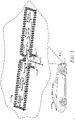
- FIG. 1 an example waveguide 100, in accordance with one or more implementations of the present disclosure, is shown.
- the waveguide 100 is part of an apparatus 102.
- the apparatus 102 may include other components (e.g., probes, receivers, transmitters, transceivers) for communicating electromagnetic fields 104 and may be situated within a vehicle 118.
- the transceiver (not shown in Fig. 1 ) may be operable upon actuation to interact with electromagnetic waves or fields associated with the waveguide 100.
- the transceiver may include one or more components, including a receiver, transmitter, or both.
- a coupling 106 is a link between the transceiver and the waveguide 100 that cooperates with an opening 108 defined by the waveguide 100, forming an antenna assembly. Examples of the coupling 106 may include a coaxial cable, conduit, various implements, or combinations thereof.
- the waveguide 100 may be formed of various conductive portions, conductors, which may be conductive layers (shown in Fig. 2 ), and vias 110 conductively connecting the conductive layers about a substrate 112.
- the substrate 112 may be a dielectric.
- the waveguide 100 includes a plurality of vias 110, although for brevity and clarity, only one via 110 is designated.
- a conductive connection may correspond to various suitable electrical connections, including different application technologies and processes. Although many materials conduct to some degree, a conductive connection is one that is constructed or architected to conduct electrons, though electrons may not be routinely conducted.
- a conductive connection may include various associations of parts having, for example, a conductivity greater than 1.00 siemens per meter at 20 degrees centigrade (S/m at 20 °C) between the parts. Conductive connection does not necessarily require unitarily implemented conductors. Further, a conductive connection may include various suitable breaks and interruptions, including interconnections, switches, buffers, and other implements to provide conductive connections between two or more components. As such, a dielectric may include materials that have conductivities less than 1.00 S/m at 20 °C.
- the waveguide 100 may include an aperture 114 for conveying the electromagnetic fields 104 to an environment 116 of the waveguide 100.
- the aperture 114 is illustrated as one slot within Fig. 1
- the aperture 114 may be defined by one or more slots, holes, openings, apertures, ports, various other defined shapes, or various combinations thereof.
- the slots may have matching shapes and sizes.
- at least one of the slots may be different in shape or size from another.
- the waveguide 100 may be situated in an environment 116 having an atmosphere or surroundings.
- the waveguide 100 may be situated within a bumper or exterior of a vehicle.
- the environment 116 may change, depending on the circumstances of its position. For instance, a vehicle traveling through inclement weather may have an environment 116 that is more parts water than a vehicle traveling through a desert.
- a side view of an example waveguide 100 in accordance with one or more implementations of the present disclosure, is shown.
- the waveguide 100 may be formed on a substrate 112.
- the substrate 112 may extend beyond corresponding conductors that define the waveguide, and the substrate 112 may incorporate one or more additional waveguides.
- a first conductive layer 200 sandwiches the substrate 112 with a second conductive layer 202.
- the substrate 112 may be substantially planar.
- the first conductive layer 200 may be placed on one side of the substrate 112, and the second conductive layer 202 may be placed on the opposite side of the substrate 112.
- the first conductive layer 200 may then be conductively connected with the second conductive layer 202 by vias 110.
- the vias 110 may be plated, solid, through-hole, blind, buried (as shown), tented, various other implements, or various combinations thereof. As such, the vias 110 conductively connect the first conductive layer 200 with the second conductive layer 202, forming a conductor that has a substantially uniform potential with respect to a reference potential. As an example, the substantially uniform potential may be common voltage with respect to ground, where ground is the reference potential. Various reference potentials may be used (e.g., 0.0, 3.3, 5.0, 12 Volts).
- the formed conductor comprising the vias 110, the first conductive layer 200, and the second conductive layer 202 may form an electromagnetic boundary (described further below with respect to Fig. 4 ) for electromagnetic fields 104 traveling within the substrate 112 of waveguide 100.
- Fig. 2 illustrates cross-section A that depicts a cross-sectional plan view of the waveguide 100 and includes the first conductive layer 200 and second conductive layer 202.
- the cross-sectional plan views of Figs. 1 and 3-5 omit the first conductive layer 200 for clarity while maintaining the aperture 114 or array of slots defined by the first conductive layer 200 to indicate relationships between other aspects defined by the waveguide 100.
- the cross-sectional plan view is not intended to depict aspects of the waveguide 100 to scale.
- FIG. 3 a cross-sectional plan view of an example waveguide 100 according to vias 110, in accordance with one or more implementations of the present disclosure, is shown.
- the vias 110 generally surround the aperture 114 and guide the electromagnetic fields 104 from the coupling 106 through the opening 108 to the aperture 114.
- a divider 300 may be defined by the vias 110 or another conductor to guide, split, or otherwise influence the electromagnetic fields 104 between the opening 108 and the aperture 114 through the substrate 112.
- the divider 300 may define chambers for guiding the electromagnetic fields 104.
- a first chamber 302 and a second chamber 304 are defined by the vias 110, the divider 300, the first conductive layer 200, and the second conductive layer 202 (as shown in combination with Fig. 2 ).
- one via 110 of a plurality of vias 110 is designated for brevity along with impedance-matching vias 306 that are configured to match an impedance associated with electromagnetic fields (e.g., electromagnetic fields 104 from Fig. 1 ) to reduce attenuation.
- the impedance-matching vias 306 may define the opening 108, and the divider 306 may have a dimension sized similar to that of the opening 108 to direct the electromagnetic fields 104 associated therewith.
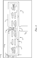
- the electromagnetic boundary 400 may be formed by the vias 110 (shown in Figs. 1 and 3 ), the first conductive layer 200, and the second conductive layer 202.
- the electromagnetic boundary 400 may also be formed by one or more other components and various combinations thereof with various combinations of the vias 110, the first conductive layer 200, or the second conductive layer 202.
- the vias 110 may be intentionally spaced and optimized to reduce the amount of conductive material used while bounding the electromagnetic fields 104 (shown in Fig 1 ).
- the electromagnetic boundary 400 may be arranged to bound electromagnetic fields 104 between the opening 108 and the aperture 114.
- the divider 300 may be defined by vias 110 or another conductor to direct electromagnetic fields 104 to the first chamber 302 and the second chamber 304. In some aspects, the divider 300 may extend toward the opening 108 to direct the electromagnetic fields 104. Extending toward the opening 108 may be at various angles with respect to the opening and refers to a general direction of the divider 300. In some implementations, the divider 300 may be oriented at angles non-perpendicular to the opening 108.
- the electromagnetic boundary 400 may be substantially rectangular, having four major corners and four major sides.
- the boundary 400 may include a first side 402 and a second side 404.
- the first side 402 may be opposite the second side 404.
- the first side 402 and the second side 404, or portions thereof, may be substantially parallel to one another or non-parallel to one another.
- the opening 108 may be substantially parallel to the second side 404.
- the opening 108 may overlap the second side 404 or be offset from the second side 404.
- the opening 108 may cooperate with the coupling 106 to convey the electromagnetic fields 104, and in one or more instances, the opening 108 may be narrower than the coupling 106 or portion thereof.
- the opening 108 may be defined between impedance-matching vias 306 to narrow the coupling 106.
- the electromagnetic boundary 400 although shown substantially rectangular, may be implemented in various forms and shapes having various quantities of sides, corners, and other features.
- the divider 300 may extend from the first side 402 toward to the second side 404.
- the divider 300 may also extend from the first side 402 toward the opening 108.
- the divider 300 may be formed by vias 110.
- the divider 300 may extend any suitable distance from the first side 402 toward the second side 404.
- the divider 300 may extend multiple different distances from the first side 402 or relative to the second side 404.
- a width 406 between the first side 402 and the second side 404 may be defined by the electromagnetic boundary 400. In implementations where the width 406 varies between the first side 402 and the second side 404, the width 406 may be defined as the maximum distance between the first side 402 and the second side 404.
- the divider 300 may extend any suitable distance (e.g., from the first side), relative to the maximum distance between the first side 402 and the second side 404. As an example, the divider 300 may extend beyond a first quartile 408 of the width 406. In another example, the divider 300 may extend beyond a first half 410 of the width 406.
- the divider 300 may form a non-linearity (e.g., a gap 412) within the first side 402.
- Vias 110 may be oriented to form only the first side 402 and the divider 300 to direct electromagnetic fields 104 from the opening 108 to the aperture 114.
- the vias 110 may be oriented to form the first side 402, the divider 300, and the second side 404 to direct electromagnetic fields 104 from the opening 108 to the aperture 114.
- the waveguide 100 may further define the aperture 114 as an array of slots 414.
- the array may include any suitable quantity of slots 414.
- the divider 300 may divide the array of slots 414 into a first portion 416 and a second portion 418.
- the first portion 416 may be associated with the first chamber 302, and the second portion 418 may be associated with the second chamber 304.
- the array of slots 414 may be defined by the first conductive layer 200, the substrate 112, or various combinations thereof.
- the divider 300 may have any suitable shape and size. As an example, the divider 300 may have a width similar to that of the opening 108. Additionally or alternatively, the divider 300 may be extended with, e.g., a squared shape, a pointed shape, a rounded shape, a semi-elliptical shape, various other contours, or combinations thereof. Further, the divider 300 may include a linear portion 420 defined by the vias 110. The linear portion 420 may be defined substantially parallel to a portion of the electromagnetic boundary 400. As an example, the linear portion 420 may be substantially parallel to the first side 402, the second side 404, or both.
- the divider 300 can also include a non-linear portion 422.
- the non-linear portion 422 may be formed by the vias 110. Further, the non-linear portion 422 may join the linear portion 420 at a vertex 424.
- An angle 426 between the linear portion 420 and the non-linear portion 422 may be less than 180 degrees. In some implementations, the angle 426 may be less than 95 degrees.
- the linear portion 420 may be substantially orthogonal to the non-linear portion 422 at the vertex 424.
- the divider 300 can also include a second non-linear portion 428.
- the second non-linear portion 428 may be formed by the vias 110.
- the second non-linear portion 428 may join the linear portion 420 at a second vertex 430.
- a second angle 432 between the linear portion 420 and the second non-linear portion 428 may be less than 180 degrees. In some implementations, the second angle 432 may also be less than 95 degrees.
- the linear portion 420 may be orthogonal to the second non-linear portion 428 at vertex 430.
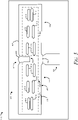
- a top view of an example waveguide 100 and bridge 500 in accordance with one or more implementations of the present disclosure, is shown.
- the divider 300 may form the gap 412 in the first side 402 of the electromagnetic boundary 400 between the first chamber 302 and the second chamber 304.
- a bridge 500 may be formed across the gap 412 to substantially linearize the non-linearity formed by the gap 412.
- the bridge 500 may be formed by vias (e.g., vias 110), similar to the divider 300.
- a manufactured apparatus 102 may include a plurality of waveguides 100 on the same die.
- the waveguides 100 may be stacked such that other couplings 106 are formed by the first side 402, directing respective electromagnetic fields 104 between respective couplings 106 and apertures 114. As such, the linearity of the first side 402 may be maintained by the bridge 500, which may reduce perturbances in the electromagnetic fields of adjacent waveguides 100.
- a method 600 for utilizing a waveguide in accordance with one or more implementations of the present disclosure is shown.
- the method 600 is shown as a set of blocks that specify operations and steps performed but are not necessarily limited to the order or combinations shown for performing the operations by the respective blocks. Further, any of one or more of the operations may be repeated, combined, reorganized, omitted, or linked to provide a wide array of additional and/or alternate methods.
- electromagnetic fields 104 are propagated through a waveguide (e.g., the waveguide 100 from Fig 1 ).
- the electromagnetic fields 104 may be driven by a transmitter through a probe or an antenna. Further, the electromagnetic fields 104 may be divided by the divider 300 into respective chambers 302, 304.
- the electromagnetic fields 104 are emitted through the aperture 114. By using the techniques described herein, squinting of the emitted electromagnetic fields 104 may be reduced.
- one or more waveguides may be used to propagate electromagnetic fields through the environment 116 from the vehicle 118. As the electromagnetic fields reflect from objects within the beam, they may return to the same waveguides or different waveguides used to receive such reflections.
- the divider 300 may reduce squint associated with the propagated and received electromagnetic fields, providing increased resolution, precision, and accuracy of the direction and range of the objects within the beam.
- the waveguide 100 may primarily be used to aid in driving the vehicle 118.
- the vehicle 118 may rely on such information, for example, for speed and orientation control. Indeed, decreasing squinting by even tenths of a degree can improve safety by improving vehicle response times.
- Fig. 7 illustrates a graph 700 depicting results of an example waveguide, in accordance with one or more implementations of the present disclosure.
- the graph 700 indicates different radiation patterns for transmitted or received signals within a gigahertz (GHZ) frequency band (e.g., 76 GHz to 78 GHz).
- a signal having a frequency of 76 GHz may be transmitted from a waveguide (e.g., waveguide 100) comprising one or more of the techniques described herein with a manufacturing tolerance of three mils for slots (e.g., slots 414) and ten mils for vias (e.g., vias 110).
- the waveguide response is depicted for five example frequencies: 76 GHz, 76.5 GHz, 77 GHz, 77.5 GHz, and 78 GHz.
- the squint or deviation from zero theta of the main lobe may be 0.5 degrees with a realized gain of 9.8 decibels (dB).
- the squint or deviation from zero theta of the main lobe may be 0.4 degrees with a realized gain of 9.9 dB for the 76.5 GHz signal.
- the squint or deviation from zero theta of the main lobe may be 0.4 degrees with a realized gain of 10.0 dB for the 77 GHz signal.
- the squint or deviation from zero theta of the main lobe may be 0.3 degrees with a realized gain of 10.2 dB.
- the squint or deviation from zero theta of the main lobe may be 0.3 degrees with a realized gain of 10.4 dB for the 78 GHz signal. Indeed, alteration of squint may be provided through the techniques described herein, providing adequate signal transmission characteristics for waveguides within manufacturing tolerances.
- Example 1 An apparatus, the apparatus comprising a waveguide defining an opening and an aperture, the opening configured to cooperate with a coupling, the aperture exposed to an environment of the waveguide.
- the waveguide comprising a conductor having a substantially uniform potential with respect to a reference potential defining an electromagnetic boundary.
- the electromagnetic boundary being arranged to bound electromagnetic fields between the opening and the aperture and configured to define a divider extending toward the opening to divide the electromagnetic boundary into a first chamber and a second chamber.
- Example 2 The apparatus of example 1, wherein the electromagnetic boundary defines a first side and a second side, the first side opposite the second side, the opening parallel to the second side and the divider extends from the first side of the electromagnetic boundary toward the opening beyond a first quartile of a width of the electromagnetic boundary that is between the first side and the second side.
- Example 3 The apparatus of any preceding example, wherein the divider extends toward the opening beyond a first half of the width of the electromagnetic boundary.
- Example 4 The apparatus of any preceding example , wherein the divider forms a gap between the first chamber and the second chamber, the gap forming a non-linearity in the electromagnetic boundary with respect to the first side, the electromagnetic boundary further defining a bridge across the gap to linearize the second side.
- Example 5 The apparatus of any preceding example, wherein: the waveguide defines the aperture as an array of slots, and the divider associates a first portion of the array with the first chamber and a second portion of the array with the second chamber.
- Example 6 The apparatus of any preceding example, wherein the divider has a linear portion.
- Example 7 The apparatus of any preceding example, wherein the linear portion is substantially parallel to a portion of the electromagnetic boundary.
- Example 8 The apparatus of any preceding example, wherein the divider has a non-linear portion, the non-linear portion joining the linear portion at a vertex with an angle less than 180 degrees.
- Example 9 The apparatus of any preceding example, wherein the linear portion is perpendicular to the non-linear portion at the vertex.
- Example 10 The apparatus of any preceding example, wherein the angle is less than 95 degrees.
- Example 11 The apparatus of any preceding example, wherein the divider has a second non-linear portion, the second non-linear portion joining the linear portion at a second vertex with a second angle less than 180 degrees.
- Example 12 The apparatus of any preceding example, wherein the linear portion is perpendicular to the second non-linear portion at the second vertex.
- Example 13 The apparatus of any preceding example, wherein the second angle is less than 95 degrees.
- Example 14 The apparatus of any preceding example, wherein the conductor comprises a first layer and a second layer, the first layer being in conductive connection with the second layer by vias conductively connecting the first layer and the second layer to form the substantially uniform potential.
- Example 15 The apparatus of any preceding example, wherein the waveguide further comprises a substrate sandwiched between the first layer and the second layer, the substrate providing an electromagnetic conduit between the opening and the second aperture.
- Example 16 The apparatus of any preceding example, wherein the substrate is a dielectric material.
- Example 17 The apparatus of any preceding example, wherein the conductor is non-contiguous from a plan view cross section perspective and wherein the electromagnetic boundary is contiguous from the plan view cross section perspective.
- Example 18 The apparatus of any preceding example, wherein the opening is defined by impedance matching vias of the electromagnetic boundary configured to match an impedance associated with the electromagnetic fields.
- Example 19 An apparatus comprising a waveguide defining an opening and an array of slots, the opening configured to cooperate with a coupling and the array of slots being exposed to an environment of the waveguide.
- the waveguide comprising a conductor having a substantially uniform potential with respect to a reference potential defining a boundary.
- the boundary arranged to bound electromagnetic fields between the opening and the array of slots and configured to define a divider extending toward the opening to divide the boundary into a first chamber bounding a first portion of the array and a second chamber bounding a second portion of the array.
- Example 20 The apparatus of any preceding example, wherein the boundary defines a first side and a second side, the first side opposite the second side, the opening parallel to the second side and the divider extends from the first side of the boundary toward the opening beyond a first quartile of a width of the boundary that is maximum between the first side and the second side.
- Example 21 A radar system configured to transmit or receive radar signals using the waveguide of any of the preceding examples.
Landscapes
- Engineering & Computer Science (AREA)
- Radar, Positioning & Navigation (AREA)
- Remote Sensing (AREA)
- Computer Networks & Wireless Communication (AREA)
- Physics & Mathematics (AREA)
- General Physics & Mathematics (AREA)
- Computer Security & Cryptography (AREA)
- Waveguide Aerials (AREA)
- Radar Systems Or Details Thereof (AREA)
- Variable-Direction Aerials And Aerial Arrays (AREA)
- Waveguides (AREA)
Abstract
Description
- This application claims the benefit under 35 U.S.C. 119(e) of
U.S. Provisional Application No. 63/127,873, filed December 18, 2020 - Some automobiles use radar and other devices that emit electromagnetic signals to detect and track objects. The electromagnetic signals are transmitted and received using one or more antennas. An antenna may be characterized in terms of pattern, which is a measure of realized gain as a function of direction. A precisely controlled pattern improves detections of other automobiles or pedestrians at narrow field of elevation, for example. In some instances, manufacturing defects may negatively affect pattern control, requiring manufacturers to discard out-of-tolerance antennas. As an example, manufacturing defects may cause pattern squinting, which can offset the realized pattern from those intended by the design and reduce precision. Squint tolerances may be on the order of tenths of degrees, requiring specific attention from designers and architects.
- This document describes techniques, apparatuses, and systems for a waveguide with squint alteration. A waveguide is described that defines an opening and an aperture. The opening is configured to cooperate with a coupling; the aperture is exposed to an environment of the waveguide. The waveguide includes a conductor having a substantially uniform potential with respect to a reference potential defining an electromagnetic boundary. The electromagnetic boundary is arranged to bound electromagnetic fields between the opening and the aperture. The electromagnetic boundary is configured to define a divider extending toward the opening to divide the electromagnetic boundary into a first chamber and a second chamber. In this way, the waveguide provides a pattern that alters the squint of the waveguide. The squint may be reduced and more normal with respect to the antenna plane.
- This document also describes other configurations and systems for providing squint alteration and other pattern-improvement techniques.
- This Summary introduces simplified concepts related to squint alternation and other pattern improvement techniques for waveguides, which are further described below in the Detailed Description and Drawings. This Summary is not intended to identify essential features of the claimed subject matter, nor is it intended for use in determining the scope of the claimed subject matter.
- The details of one or more aspects of waveguide with squint alteration are described in this document with reference to the following drawings. The same numbers may be used throughout the drawings to reference like features and components:
-
Fig. 1 illustrates an example waveguide according to a cross-sectional plan view, in accordance with one or more implementations of the present disclosure; -
Fig. 2 illustrates a side view of an example waveguide, in accordance with one or more implementations of the present disclosure; -
Fig. 3 illustrates a cross-sectional plan view of an example waveguide according to vias, in accordance with one or more implementations of the present disclosure; -
Fig. 4 illustrates a cross-sectional plan view of an example waveguide and electromagnetic boundary, in accordance with one or more implementations of the present disclosure; -
Fig. 5 illustrates a cross-sectional plan view of an example waveguide and bridge, in accordance with one or more implementations of the present disclosure; -
Fig. 6 illustrates a method for utilizing a waveguide, in accordance with one or more implementations of the present disclosure; and -
Fig. 7 illustrates a graph depicting results of an example waveguide, in accordance with one or more implementations of the present disclosure. - Electromagnetic systems are a common sensing technology used in many industries, including the automotive industry, acquiring information about the surrounding environment or transceiving data. An antenna, such as one described herein, may be employed in such systems to transmit and receive electromagnetic signals. A radar system may use multiple antenna elements in an array to provide increased gain and directivity over what can be achieved using a single antenna element. As described herein, signals from the individual elements are combined with appropriate phases and weighted amplitudes to provide a desired antenna-reception pattern during reception. The antenna arrays are also used in transmission, splitting signal power amongst the elements, using appropriate phases and weighted amplitudes to provide a desired antenna-transmission pattern during transmission.
- Consider, for example, a waveguide employed to transfer electromagnetic energy. The waveguide may include an opening, which may be associated with a coupling. As an example, the coupling may provide an additional conduit for controlling electromagnetic waves associated with the waveguide. The coupling may provide electromagnetic-field access between an aperture of the waveguide exposed to the environment and a probe associated with the waveguide for transceiving electromagnetic signals with transceiver circuitry. The aperture may be an array of slots, and the waveguide may bound electromagnetic waves between the aperture and the opening in a way to reduce squinting of the transmitted or received electromagnetic signals.
- The waveguide can include an array of radiating slots of various shapes, which may be arranged to provide desired phasing, combining, or splitting of signals and energy. To provide equal power distribution, minimize squinting, and reduce signal error, the slots may be divided into groups. In an example, the waveguide may have a T-shape with slots divided into two different groups, one for each side of the T. As electromagnetic waves bounce down the coupling and through the waveguide, if the waves are allowed to unevenly distribute to one side or the other of the T, this can result in squinting the direction of the resulting beam. This squinting may cause uncertainty in detections and may be particularly detrimental in an automotive context (e.g., accurate detection of objects associated with a roadway). A way to ensure equal power distribution to prevent squinting and the negative effects associated with squinting is desired.
- In this way, the present disclosure describes squint alteration associated with a waveguide. The wave guide may be defined in a T-shape and cooperate with a divider that act together to reduce squinting so as to equally divide or join the electromagnetic waves and prevent uneven distributions to one side or the other of the T. Application of this and other examples provided in this disclosure may increase radiation performance of a waveguide. These are but a few examples of how the described techniques and devices may be used to improve conventional waveguides.
- In
Fig. 1 , anexample waveguide 100, in accordance with one or more implementations of the present disclosure, is shown. Thewaveguide 100 is part of anapparatus 102. Theapparatus 102 may include other components (e.g., probes, receivers, transmitters, transceivers) for communicatingelectromagnetic fields 104 and may be situated within avehicle 118. In some implementations, the transceiver (not shown inFig. 1 ) may be operable upon actuation to interact with electromagnetic waves or fields associated with thewaveguide 100. - The transceiver may include one or more components, including a receiver, transmitter, or both. A
coupling 106 is a link between the transceiver and thewaveguide 100 that cooperates with anopening 108 defined by thewaveguide 100, forming an antenna assembly. Examples of thecoupling 106 may include a coaxial cable, conduit, various implements, or combinations thereof. - The
waveguide 100 may be formed of various conductive portions, conductors, which may be conductive layers (shown inFig. 2 ), and vias 110 conductively connecting the conductive layers about asubstrate 112. Thesubstrate 112 may be a dielectric. In the illustrated example, thewaveguide 100 includes a plurality ofvias 110, although for brevity and clarity, only one via 110 is designated. It should be appreciated that a conductive connection may correspond to various suitable electrical connections, including different application technologies and processes. Although many materials conduct to some degree, a conductive connection is one that is constructed or architected to conduct electrons, though electrons may not be routinely conducted. A conductive connection may include various associations of parts having, for example, a conductivity greater than 1.00 siemens per meter at 20 degrees centigrade (S/m at 20 °C) between the parts. Conductive connection does not necessarily require unitarily implemented conductors. Further, a conductive connection may include various suitable breaks and interruptions, including interconnections, switches, buffers, and other implements to provide conductive connections between two or more components. As such, a dielectric may include materials that have conductivities less than 1.00 S/m at 20 °C. - The
waveguide 100 may include anaperture 114 for conveying theelectromagnetic fields 104 to anenvironment 116 of thewaveguide 100. Although theaperture 114 is illustrated as one slot withinFig. 1 , theaperture 114 may be defined by one or more slots, holes, openings, apertures, ports, various other defined shapes, or various combinations thereof. In one instance, the slots may have matching shapes and sizes. In another instance, at least one of the slots may be different in shape or size from another. Thewaveguide 100 may be situated in anenvironment 116 having an atmosphere or surroundings. As an example, thewaveguide 100 may be situated within a bumper or exterior of a vehicle. Theenvironment 116 may change, depending on the circumstances of its position. For instance, a vehicle traveling through inclement weather may have anenvironment 116 that is more parts water than a vehicle traveling through a desert. - In
Fig. 2 , a side view of anexample waveguide 100, in accordance with one or more implementations of the present disclosure, is shown. In aspects, thewaveguide 100 may be formed on asubstrate 112. Although omitted for clarity, thesubstrate 112 may extend beyond corresponding conductors that define the waveguide, and thesubstrate 112 may incorporate one or more additional waveguides. In the illustrated example, a firstconductive layer 200 sandwiches thesubstrate 112 with a secondconductive layer 202. In aspects, thesubstrate 112 may be substantially planar. During manufacturing, the firstconductive layer 200 may be placed on one side of thesubstrate 112, and the secondconductive layer 202 may be placed on the opposite side of thesubstrate 112. The firstconductive layer 200 may then be conductively connected with the secondconductive layer 202 byvias 110. - The
vias 110 may be plated, solid, through-hole, blind, buried (as shown), tented, various other implements, or various combinations thereof. As such, thevias 110 conductively connect the firstconductive layer 200 with the secondconductive layer 202, forming a conductor that has a substantially uniform potential with respect to a reference potential. As an example, the substantially uniform potential may be common voltage with respect to ground, where ground is the reference potential. Various reference potentials may be used (e.g., 0.0, 3.3, 5.0, 12 Volts). The formed conductor comprising thevias 110, the firstconductive layer 200, and the secondconductive layer 202 may form an electromagnetic boundary (described further below with respect toFig. 4 ) forelectromagnetic fields 104 traveling within thesubstrate 112 ofwaveguide 100. -
Fig. 2 illustrates cross-section A that depicts a cross-sectional plan view of thewaveguide 100 and includes the firstconductive layer 200 and secondconductive layer 202. The cross-sectional plan views ofFigs. 1 and3-5 omit the firstconductive layer 200 for clarity while maintaining theaperture 114 or array of slots defined by the firstconductive layer 200 to indicate relationships between other aspects defined by thewaveguide 100. The cross-sectional plan view is not intended to depict aspects of thewaveguide 100 to scale. - Referring to
Fig. 3 , a cross-sectional plan view of anexample waveguide 100 according tovias 110, in accordance with one or more implementations of the present disclosure, is shown. As shown, thevias 110 generally surround theaperture 114 and guide theelectromagnetic fields 104 from thecoupling 106 through theopening 108 to theaperture 114. Adivider 300 may be defined by thevias 110 or another conductor to guide, split, or otherwise influence theelectromagnetic fields 104 between theopening 108 and theaperture 114 through thesubstrate 112. In aspects, thedivider 300 may define chambers for guiding theelectromagnetic fields 104. For example, afirst chamber 302 and asecond chamber 304 are defined by thevias 110, thedivider 300, the firstconductive layer 200, and the second conductive layer 202 (as shown in combination withFig. 2 ). Accordingly, one via 110 of a plurality ofvias 110 is designated for brevity along with impedance-matching vias 306 that are configured to match an impedance associated with electromagnetic fields (e.g.,electromagnetic fields 104 fromFig. 1 ) to reduce attenuation. For instance, the impedance-matching vias 306 may define theopening 108, and the divider 306 may have a dimension sized similar to that of theopening 108 to direct theelectromagnetic fields 104 associated therewith. - Turning to
Fig. 4 , a cross-sectional plan view of anexample waveguide 100 and anelectromagnetic boundary 400, in accordance with one or more implementations of the present disclosure, is shown. Theelectromagnetic boundary 400 may be formed by the vias 110 (shown inFigs. 1 and3 ), the firstconductive layer 200, and the secondconductive layer 202. Theelectromagnetic boundary 400 may also be formed by one or more other components and various combinations thereof with various combinations of thevias 110, the firstconductive layer 200, or the secondconductive layer 202. Thevias 110 may be intentionally spaced and optimized to reduce the amount of conductive material used while bounding the electromagnetic fields 104 (shown inFig 1 ). Theelectromagnetic boundary 400 may be arranged to boundelectromagnetic fields 104 between theopening 108 and theaperture 114. Thedivider 300 may be defined byvias 110 or another conductor to directelectromagnetic fields 104 to thefirst chamber 302 and thesecond chamber 304. In some aspects, thedivider 300 may extend toward theopening 108 to direct theelectromagnetic fields 104. Extending toward theopening 108 may be at various angles with respect to the opening and refers to a general direction of thedivider 300. In some implementations, thedivider 300 may be oriented at angles non-perpendicular to theopening 108. - As illustrated, the
electromagnetic boundary 400 may be substantially rectangular, having four major corners and four major sides. For example, theboundary 400 may include afirst side 402 and asecond side 404. Thefirst side 402 may be opposite thesecond side 404. Thefirst side 402 and thesecond side 404, or portions thereof, may be substantially parallel to one another or non-parallel to one another. Theopening 108 may be substantially parallel to thesecond side 404. Theopening 108 may overlap thesecond side 404 or be offset from thesecond side 404. In an example, theopening 108 may cooperate with thecoupling 106 to convey theelectromagnetic fields 104, and in one or more instances, theopening 108 may be narrower than thecoupling 106 or portion thereof. As an example, theopening 108 may be defined between impedance-matching vias 306 to narrow thecoupling 106. Theelectromagnetic boundary 400, although shown substantially rectangular, may be implemented in various forms and shapes having various quantities of sides, corners, and other features. - The
divider 300 may extend from thefirst side 402 toward to thesecond side 404. Thedivider 300 may also extend from thefirst side 402 toward theopening 108. Thedivider 300 may be formed byvias 110. In aspects, thedivider 300 may extend any suitable distance from thefirst side 402 toward thesecond side 404. In other aspects, depending on the shape or contour, thedivider 300 may extend multiple different distances from thefirst side 402 or relative to thesecond side 404. Awidth 406 between thefirst side 402 and thesecond side 404 may be defined by theelectromagnetic boundary 400. In implementations where thewidth 406 varies between thefirst side 402 and thesecond side 404, thewidth 406 may be defined as the maximum distance between thefirst side 402 and thesecond side 404. In such implementations, thedivider 300 may extend any suitable distance (e.g., from the first side), relative to the maximum distance between thefirst side 402 and thesecond side 404. As an example, thedivider 300 may extend beyond afirst quartile 408 of thewidth 406. In another example, thedivider 300 may extend beyond afirst half 410 of thewidth 406. - In some implementations, the
divider 300 may form a non-linearity (e.g., a gap 412) within thefirst side 402.Vias 110 may be oriented to form only thefirst side 402 and thedivider 300 to directelectromagnetic fields 104 from theopening 108 to theaperture 114. In another example, thevias 110 may be oriented to form thefirst side 402, thedivider 300, and thesecond side 404 to directelectromagnetic fields 104 from theopening 108 to theaperture 114. - The
waveguide 100 may further define theaperture 114 as an array ofslots 414. The array may include any suitable quantity ofslots 414. Thedivider 300 may divide the array ofslots 414 into afirst portion 416 and asecond portion 418. Thefirst portion 416 may be associated with thefirst chamber 302, and thesecond portion 418 may be associated with thesecond chamber 304. The array ofslots 414 may be defined by the firstconductive layer 200, thesubstrate 112, or various combinations thereof. - The
divider 300 may have any suitable shape and size. As an example, thedivider 300 may have a width similar to that of theopening 108. Additionally or alternatively, thedivider 300 may be extended with, e.g., a squared shape, a pointed shape, a rounded shape, a semi-elliptical shape, various other contours, or combinations thereof. Further, thedivider 300 may include alinear portion 420 defined by thevias 110. Thelinear portion 420 may be defined substantially parallel to a portion of theelectromagnetic boundary 400. As an example, thelinear portion 420 may be substantially parallel to thefirst side 402, thesecond side 404, or both. - The
divider 300 can also include anon-linear portion 422. Thenon-linear portion 422 may be formed by thevias 110. Further, thenon-linear portion 422 may join thelinear portion 420 at a vertex 424. Anangle 426 between thelinear portion 420 and thenon-linear portion 422 may be less than 180 degrees. In some implementations, theangle 426 may be less than 95 degrees. As an example, thelinear portion 420 may be substantially orthogonal to thenon-linear portion 422 at the vertex 424. - The
divider 300 can also include a secondnon-linear portion 428. The secondnon-linear portion 428 may be formed by thevias 110. The secondnon-linear portion 428 may join thelinear portion 420 at a second vertex 430. A second angle 432 between thelinear portion 420 and the secondnon-linear portion 428 may be less than 180 degrees. In some implementations, the second angle 432 may also be less than 95 degrees. As an example, thelinear portion 420 may be orthogonal to the secondnon-linear portion 428 at vertex 430. - Turning to
Fig. 5 , a top view of anexample waveguide 100 andbridge 500, in accordance with one or more implementations of the present disclosure, is shown. Thedivider 300 may form thegap 412 in thefirst side 402 of theelectromagnetic boundary 400 between thefirst chamber 302 and thesecond chamber 304. In aspects, abridge 500 may be formed across thegap 412 to substantially linearize the non-linearity formed by thegap 412. Thebridge 500 may be formed by vias (e.g., vias 110), similar to thedivider 300. As an example, amanufactured apparatus 102 may include a plurality ofwaveguides 100 on the same die. Thewaveguides 100 may be stacked such thatother couplings 106 are formed by thefirst side 402, directing respectiveelectromagnetic fields 104 betweenrespective couplings 106 andapertures 114. As such, the linearity of thefirst side 402 may be maintained by thebridge 500, which may reduce perturbances in the electromagnetic fields ofadjacent waveguides 100. - Turning to
Fig. 6 , amethod 600 for utilizing a waveguide, in accordance with one or more implementations of the present disclosure is shown. Themethod 600 is shown as a set of blocks that specify operations and steps performed but are not necessarily limited to the order or combinations shown for performing the operations by the respective blocks. Further, any of one or more of the operations may be repeated, combined, reorganized, omitted, or linked to provide a wide array of additional and/or alternate methods. In portions of the following discussion, reference may be made to the examples of the preceding figures, reference to which is made for example only. The techniques are not limited to performance by one entity or multiple entities operating on one device. - In
block 602,electromagnetic fields 104 are propagated through a waveguide (e.g., thewaveguide 100 fromFig 1 ). In an example, theelectromagnetic fields 104 may be driven by a transmitter through a probe or an antenna. Further, theelectromagnetic fields 104 may be divided by thedivider 300 intorespective chambers block 604, theelectromagnetic fields 104 are emitted through theaperture 114. By using the techniques described herein, squinting of the emittedelectromagnetic fields 104 may be reduced. In an example, one or more waveguides may be used to propagate electromagnetic fields through theenvironment 116 from thevehicle 118. As the electromagnetic fields reflect from objects within the beam, they may return to the same waveguides or different waveguides used to receive such reflections. Thedivider 300 may reduce squint associated with the propagated and received electromagnetic fields, providing increased resolution, precision, and accuracy of the direction and range of the objects within the beam. Although also envisioned for use in other applications, thewaveguide 100 may primarily be used to aid in driving thevehicle 118. Thevehicle 118 may rely on such information, for example, for speed and orientation control. Indeed, decreasing squinting by even tenths of a degree can improve safety by improving vehicle response times. -
Fig. 7 illustrates agraph 700 depicting results of an example waveguide, in accordance with one or more implementations of the present disclosure. Thegraph 700 indicates different radiation patterns for transmitted or received signals within a gigahertz (GHZ) frequency band (e.g., 76 GHz to 78 GHz). As an example, a signal having a frequency of 76 GHz may be transmitted from a waveguide (e.g., waveguide 100) comprising one or more of the techniques described herein with a manufacturing tolerance of three mils for slots (e.g., slots 414) and ten mils for vias (e.g., vias 110). The waveguide response is depicted for five example frequencies: 76 GHz, 76.5 GHz, 77 GHz, 77.5 GHz, and 78 GHz. - For 76 GHz, the squint or deviation from zero theta of the main lobe may be 0.5 degrees with a realized gain of 9.8 decibels (dB). The squint or deviation from zero theta of the main lobe may be 0.4 degrees with a realized gain of 9.9 dB for the 76.5 GHz signal. As another example, the squint or deviation from zero theta of the main lobe may be 0.4 degrees with a realized gain of 10.0 dB for the 77 GHz signal. For the 77.5 GHz signal, the squint or deviation from zero theta of the main lobe may be 0.3 degrees with a realized gain of 10.2 dB. further, the squint or deviation from zero theta of the main lobe may be 0.3 degrees with a realized gain of 10.4 dB for the 78 GHz signal. Indeed, alteration of squint may be provided through the techniques described herein, providing adequate signal transmission characteristics for waveguides within manufacturing tolerances.
- Example 1. An apparatus, the apparatus comprising a waveguide defining an opening and an aperture, the opening configured to cooperate with a coupling, the aperture exposed to an environment of the waveguide. The waveguide comprising a conductor having a substantially uniform potential with respect to a reference potential defining an electromagnetic boundary. The electromagnetic boundary being arranged to bound electromagnetic fields between the opening and the aperture and configured to define a divider extending toward the opening to divide the electromagnetic boundary into a first chamber and a second chamber.
- Example 2. The apparatus of example 1, wherein the electromagnetic boundary defines a first side and a second side, the first side opposite the second side, the opening parallel to the second side and the divider extends from the first side of the electromagnetic boundary toward the opening beyond a first quartile of a width of the electromagnetic boundary that is between the first side and the second side.
- Example 3. The apparatus of any preceding example, wherein the divider extends toward the opening beyond a first half of the width of the electromagnetic boundary.
- Example 4. The apparatus of any preceding example , wherein the divider forms a gap between the first chamber and the second chamber, the gap forming a non-linearity in the electromagnetic boundary with respect to the first side, the electromagnetic boundary further defining a bridge across the gap to linearize the second side.
- Example 5. The apparatus of any preceding example, wherein: the waveguide defines the aperture as an array of slots, and the divider associates a first portion of the array with the first chamber and a second portion of the array with the second chamber.
- Example 6. The apparatus of any preceding example, wherein the divider has a linear portion.
- Example 7. The apparatus of any preceding example, wherein the linear portion is substantially parallel to a portion of the electromagnetic boundary.
- Example 8. The apparatus of any preceding example, wherein the divider has a non-linear portion, the non-linear portion joining the linear portion at a vertex with an angle less than 180 degrees.
- Example 9. The apparatus of any preceding example, wherein the linear portion is perpendicular to the non-linear portion at the vertex.
- Example 10. The apparatus of any preceding example, wherein the angle is less than 95 degrees.
- Example 11. The apparatus of any preceding example, wherein the divider has a second non-linear portion, the second non-linear portion joining the linear portion at a second vertex with a second angle less than 180 degrees.
- Example 12. The apparatus of any preceding example, wherein the linear portion is perpendicular to the second non-linear portion at the second vertex.
- Example 13. The apparatus of any preceding example, wherein the second angle is less than 95 degrees.
- Example 14. The apparatus of any preceding example, wherein the conductor comprises a first layer and a second layer, the first layer being in conductive connection with the second layer by vias conductively connecting the first layer and the second layer to form the substantially uniform potential.
- Example 15. The apparatus of any preceding example, wherein the waveguide further comprises a substrate sandwiched between the first layer and the second layer, the substrate providing an electromagnetic conduit between the opening and the second aperture.
- Example 16. The apparatus of any preceding example, wherein the substrate is a dielectric material.
- Example 17. The apparatus of any preceding example, wherein the conductor is non-contiguous from a plan view cross section perspective and wherein the electromagnetic boundary is contiguous from the plan view cross section perspective.
- Example 18. The apparatus of any preceding example, wherein the opening is defined by impedance matching vias of the electromagnetic boundary configured to match an impedance associated with the electromagnetic fields.
- Example 19. An apparatus comprising a waveguide defining an opening and an array of slots, the opening configured to cooperate with a coupling and the array of slots being exposed to an environment of the waveguide. The waveguide comprising a conductor having a substantially uniform potential with respect to a reference potential defining a boundary. The boundary arranged to bound electromagnetic fields between the opening and the array of slots and configured to define a divider extending toward the opening to divide the boundary into a first chamber bounding a first portion of the array and a second chamber bounding a second portion of the array.
- Example 20. The apparatus of any preceding example, wherein the boundary defines a first side and a second side, the first side opposite the second side, the opening parallel to the second side and the divider extends from the first side of the boundary toward the opening beyond a first quartile of a width of the boundary that is maximum between the first side and the second side.
- Example 21. A radar system configured to transmit or receive radar signals using the waveguide of any of the preceding examples.
- Although implementations of techniques for, and apparatuses or systems enabling, a waveguide with squint alteration have been described in language specific to features and/or methods, it is to be understood that the subject of the appended claims is not necessarily limited to the specific features or methods described. Rather, the specific features and methods are disclosed as example implementations enabling a waveguide with squint alteration.
Claims (15)
- An apparatus, the apparatus comprising:
a waveguide defining an opening and an aperture, the opening configured to cooperate with a coupling, the aperture exposed to an environment of the waveguide, the waveguide comprising a conductor having a substantially uniform potential with respect to a reference potential defining an electromagnetic boundary, the electromagnetic boundary:arranged to bound electromagnetic fields between the opening and the aperture; andconfigured to define a divider extending toward the opening to divide the electromagnetic boundary into a first chamber and a second chamber. - The apparatus of claim 1, wherein the electromagnetic boundary defines a first side and a second side, the first side opposite the second side, the opening parallel to the second side and the divider extends from the first side of the electromagnetic boundary toward the opening beyond a first quartile of a width of the electromagnetic boundary that is between the first side and the second side.
- The apparatus of claim 2, wherein the divider extends toward the opening beyond a first half of the width of the electromagnetic boundary.
- The apparatus of claim 2 or 3, wherein the divider forms a gap between the first chamber and the second chamber, the gap forming a non-linearity in the electromagnetic boundary with respect to the first side, the electromagnetic boundary further defining a bridge across the gap to linearize the second side.
- The apparatus of any of claims 1-4, wherein:the waveguide defines the aperture as an array of slots; andthe divider associates a first portion of the array with the first chamber and a second portion of the array with the second chamber.
- The apparatus of any of claims 1-5, wherein the divider has a linear portion.
- The apparatus of claim 6, wherein the linear portion is substantially parallel to a portion of the electromagnetic boundary.
- The apparatus of claim 6 or 7, wherein the divider has a non-linear portion, the non-linear portion joining the linear portion at a vertex with an angle less than 180 degrees.
- The apparatus of any of claim 6-8, wherein the linear portion is perpendicular to the non-linear portion at the vertex.
- The apparatus of claim 8 or 9, wherein the divider has a second non-linear portion, the second non-linear portion joining the linear portion at a second vertex with a second angle less than 180 degrees.
- The apparatus of claim 10, wherein the linear portion is perpendicular to the second non-linear portion at the second vertex.
- The apparatus of any of claims 1-11, wherein the conductor comprises a first layer and a second layer, the first layer being in conductive connection with the second layer by vias conductively connecting the first layer and the second layer to form the substantially uniform potential.
- The apparatus of claim 12, wherein the waveguide further comprises a substrate sandwiched between the first layer and the second layer, the substrate providing an electromagnetic conduit between the opening and the aperture.
- The apparatus of claim 13, wherein the substrate is a dielectric material.
- A radar system configured to transmit or receive radar signals using the waveguide of any of claims 1-14.
Applications Claiming Priority (2)
| Application Number | Priority Date | Filing Date | Title |
|---|---|---|---|
| US202063127873P | 2020-12-18 | 2020-12-18 | |
| US17/205,710 US11681015B2 (en) | 2020-12-18 | 2021-03-18 | Waveguide with squint alteration |
Publications (2)
| Publication Number | Publication Date |
|---|---|
| EP4016739A1 true EP4016739A1 (en) | 2022-06-22 |
| EP4016739B1 EP4016739B1 (en) | 2026-02-18 |
Family
ID=78819434
Family Applications (1)
| Application Number | Title | Priority Date | Filing Date |
|---|---|---|---|
| EP21211452.4A Active EP4016739B1 (en) | 2020-12-18 | 2021-11-30 | Waveguide with squint alteration |
Country Status (3)
| Country | Link |
|---|---|
| US (1) | US11681015B2 (en) |
| EP (1) | EP4016739B1 (en) |
| CN (1) | CN114649660B (en) |
Families Citing this family (11)
| Publication number | Priority date | Publication date | Assignee | Title |
|---|---|---|---|---|
| DE112019007271T5 (en) * | 2019-04-29 | 2022-05-05 | Shanghai Baolong Automotive Corporation | Array antenna of an onboard millimeter wave radar |
| US11901601B2 (en) | 2020-12-18 | 2024-02-13 | Aptiv Technologies Limited | Waveguide with a zigzag for suppressing grating lobes |
| US11749883B2 (en) | 2020-12-18 | 2023-09-05 | Aptiv Technologies Limited | Waveguide with radiation slots and parasitic elements for asymmetrical coverage |
| US12058804B2 (en) | 2021-02-09 | 2024-08-06 | Aptiv Technologies AG | Formed waveguide antennas of a radar assembly |
| US11962085B2 (en) | 2021-05-13 | 2024-04-16 | Aptiv Technologies AG | Two-part folded waveguide having a sinusoidal shape channel including horn shape radiating slots formed therein which are spaced apart by one-half wavelength |
| US11616282B2 (en) | 2021-08-03 | 2023-03-28 | Aptiv Technologies Limited | Transition between a single-ended port and differential ports having stubs that match with input impedances of the single-ended and differential ports |
| US12456816B2 (en) | 2022-05-02 | 2025-10-28 | Aptiv Technologies AG | Waveguide with slot antennas and reflectors |
| US12537308B2 (en) | 2023-01-24 | 2026-01-27 | Aptiv Technologies AG | Symmetrical two-piece waveguide |
| US12148992B2 (en) | 2023-01-25 | 2024-11-19 | Aptiv Technologies AG | Hybrid horn waveguide antenna |
| US12627020B2 (en) | 2023-05-18 | 2026-05-12 | Aptiv Technologies AG | Waveguide with a curved-wall low-pass filter |
| US12689130B2 (en) * | 2024-03-12 | 2026-07-21 | Nxp B.V. | Frequency beam-steered substrate-integrated antennas |
Family Cites Families (140)
| Publication number | Priority date | Publication date | Assignee | Title |
|---|---|---|---|---|
| US3328800A (en) | 1964-03-12 | 1967-06-27 | North American Aviation Inc | Slot antenna utilizing variable standing wave pattern for controlling slot excitation |
| US3462713A (en) | 1967-07-19 | 1969-08-19 | Bell Telephone Labor Inc | Waveguide-stripline transducer |
| US3594806A (en) | 1969-04-02 | 1971-07-20 | Hughes Aircraft Co | Dipole augmented slot radiating elements |
| US3579149A (en) | 1969-12-08 | 1971-05-18 | Westinghouse Electric Corp | Waveguide to stripline transition means |
| NL7609903A (en) | 1976-09-07 | 1978-03-09 | Philips Nv | MICROWAVE DEVICE FOR CONVERTING A WAVE PIPE INTO A MICROSTRIP GUIDE STRUCTURE. |
| US4291312A (en) | 1977-09-28 | 1981-09-22 | The United States Of America As Represented By The Secretary Of The Navy | Dual ground plane coplanar fed microstrip antennas |
| US4453142A (en) | 1981-11-02 | 1984-06-05 | Motorola Inc. | Microstrip to waveguide transition |
| US4562416A (en) | 1984-05-31 | 1985-12-31 | Sanders Associates, Inc. | Transition from stripline to waveguide |
| US4590480A (en) | 1984-08-31 | 1986-05-20 | Rca Corporation | Broadcast antenna which radiates horizontal polarization towards distant locations and circular polarization towards nearby locations |
| GB2463711B (en) | 1987-03-31 | 2010-09-29 | Dassault Electronique | Double polarization flat array antenna |
| US5030965A (en) | 1989-11-15 | 1991-07-09 | Hughes Aircraft Company | Slot antenna having controllable polarization |
| US5047738A (en) | 1990-10-09 | 1991-09-10 | Hughes Aircraft Company | Ridged waveguide hybrid |
| IL107582A (en) | 1993-11-12 | 1998-02-08 | Ramot Ramatsity Authority For | Slotted waveguide array antennas |
| US5986527A (en) | 1995-03-28 | 1999-11-16 | Murata Manufacturing Co., Ltd. | Planar dielectric line and integrated circuit using the same line |
| JP3366552B2 (en) | 1997-04-22 | 2003-01-14 | 京セラ株式会社 | Dielectric waveguide line and multilayer wiring board including the same |
| AU7097398A (en) * | 1997-12-29 | 1999-07-19 | Chung Hsin-Hsien | Low cost high performance portable phased array antenna system for satellite communication |
| CA2292064C (en) | 1998-12-25 | 2003-08-19 | Murata Manufacturing Co., Ltd. | Line transition device between dielectric waveguide and waveguide, and oscillator and transmitter using the same |
| US6166701A (en) | 1999-08-05 | 2000-12-26 | Raytheon Company | Dual polarization antenna array with radiating slots and notch dipole elements sharing a common aperture |
| US6590477B1 (en) | 1999-10-29 | 2003-07-08 | Fci Americas Technology, Inc. | Waveguides and backplane systems with at least one mode suppression gap |
| AU2000277887A1 (en) | 2000-10-18 | 2002-04-29 | Nokia Corporation | Waveguide to stripline transition |
| WO2002052674A1 (en) | 2000-12-21 | 2002-07-04 | Paratek Microwave, Inc. | Waveguide to microstrip transition |
| US6967347B2 (en) | 2001-05-21 | 2005-11-22 | The Regents Of The University Of Colorado | Terahertz interconnect system and applications |
| JP3858023B2 (en) | 2001-11-20 | 2006-12-13 | アンリツ株式会社 | Waveguide slot radiator with configuration for ease of manufacture |
| JP2003289201A (en) | 2002-03-28 | 2003-10-10 | Anritsu Corp | Connection conversion structure between post-wall waveguide and hollow waveguide |
| US7091919B2 (en) | 2003-12-30 | 2006-08-15 | Spx Corporation | Apparatus and method to increase apparent resonant slot length in a slotted coaxial antenna |
| US7034774B2 (en) | 2004-04-22 | 2006-04-25 | Northrop Grumman Corporation | Feed structure and antenna structures incorporating such feed structures |
| US7098070B2 (en) | 2004-11-16 | 2006-08-29 | International Business Machines Corporation | Device and method for fabricating double-sided SOI wafer scale package with through via connections |
| CN2796131Y (en) | 2005-05-30 | 2006-07-12 | 东南大学 | Multilayer substrate integrated wave guide elliptical response filter |
| FR2886773B1 (en) | 2005-06-03 | 2007-09-07 | Thales Sa | DISPERSIVE ANTENNA IN FREQUENCY APPLIED IN PARTICULAR TO WEATHER RADAR |
| US7460084B2 (en) | 2005-10-19 | 2008-12-02 | Northrop Grumman Corporation | Radio frequency holographic transformer |
| WO2007114391A1 (en) | 2006-03-31 | 2007-10-11 | Kyocera Corporation | Dielectric waveguide device; phase shifter, high frequency switch, and attenuator provided with dielectric waveguide device; and method of manufacturing high frequency transmitter, high frequency receiver, high frequency transmitter/receiver and radar device, array antenna, and dielectric waveguide device |
| JP2009539411A (en) | 2006-06-12 | 2009-11-19 | パシフィック バイオサイエンシーズ オブ カリフォルニア, インコーポレイテッド | Substrates for performing analytical reactions |
| CN101584080A (en) * | 2006-11-17 | 2009-11-18 | 韦夫班德尔公司 | Integrated waveguide antenna array |
| KR100846872B1 (en) | 2006-11-17 | 2008-07-16 | 한국전자통신연구원 | Apparatus for the transition of dielectric waveguide and transmission line in millimeter wave band |
| JP4365852B2 (en) | 2006-11-30 | 2009-11-18 | 株式会社日立製作所 | Waveguide structure |
| EP1936741A1 (en) | 2006-12-22 | 2008-06-25 | Sony Deutschland GmbH | Flexible substrate integrated waveguides |
| US8231284B2 (en) | 2007-03-26 | 2012-07-31 | International Business Machines Corporation | Ultra-high bandwidth, multiple-channel full-duplex, single-chip CMOS optical transceiver |
| GB0706296D0 (en) | 2007-03-30 | 2007-05-09 | Nortel Networks Ltd | Low cost lightweight antenna technology |
| US7768457B2 (en) | 2007-06-22 | 2010-08-03 | Vubiq, Inc. | Integrated antenna and chip package and method of manufacturing thereof |
| JP5179513B2 (en) | 2007-12-28 | 2013-04-10 | 京セラ株式会社 | High-frequency transmission line connection structure, wiring board, high-frequency module, and radar device |
| EP2249437B1 (en) | 2008-02-28 | 2019-02-20 | Mitsubishi Electric Corporation | Waveguide slot array antenna apparatus |
| CA2629035A1 (en) | 2008-03-27 | 2009-09-27 | Her Majesty The Queen In Right Of Canada, As Represented By The Minister Of Industry, Through The Communications Research Centre Canada | Waveguide filter with broad stopband based on sugstrate integrated waveguide scheme |
| JP5172481B2 (en) | 2008-06-05 | 2013-03-27 | 株式会社東芝 | Short slot directional coupler with post-wall waveguide, butler matrix and on-vehicle radar antenna using the same |
| US8089327B2 (en) | 2009-03-09 | 2012-01-03 | Toyota Motor Engineering & Manufacturing North America, Inc. | Waveguide to plural microstrip transition |
| KR101327375B1 (en) | 2009-03-31 | 2013-11-08 | 쿄세라 코포레이션 | Waveguide structure, high frequency module including waveguide structure, and radar apparatus |
| CN201383535Y (en) | 2009-04-01 | 2010-01-13 | 惠州市硕贝德通讯科技有限公司 | Rectangular waveguide-substrate integrated waveguide signal conversion and power divider |
| EP2427908A1 (en) | 2009-05-08 | 2012-03-14 | Telefonaktiebolaget L M Ericsson (publ) | A transition from a chip to a waveguide port |
| US8604990B1 (en) | 2009-05-23 | 2013-12-10 | Victory Microwave Corporation | Ridged waveguide slot array |
| IT1398678B1 (en) | 2009-06-11 | 2013-03-08 | Mbda italia spa | SLOT SLIP ANTENNA WITH POWER SUPPLY IN WAVE GUIDE AND PROCEDURE FOR REALIZING THE SAME |
| FR2953651B1 (en) | 2009-12-07 | 2012-01-20 | Eads Defence & Security Sys | MICROFREQUENCY TRANSITION DEVICE BETWEEN A MICRO-TAPE LINE AND A RECTANGULAR WAVEGUIDE |
| US8576023B1 (en) | 2010-04-20 | 2013-11-05 | Rockwell Collins, Inc. | Stripline-to-waveguide transition including metamaterial layers and an aperture ground plane |
| US9774076B2 (en) | 2010-08-31 | 2017-09-26 | Siklu Communication ltd. | Compact millimeter-wave radio systems and methods |
| US8674885B2 (en) | 2010-08-31 | 2014-03-18 | Siklu Communication ltd. | Systems for interfacing waveguide antenna feeds with printed circuit boards |
| JP5253468B2 (en) | 2010-09-03 | 2013-07-31 | 株式会社東芝 | Antenna device and radar device |
| KR101092846B1 (en) | 2010-09-30 | 2011-12-14 | 서울대학교산학협력단 | Serial slot array antenna |
| AU2011314378A1 (en) | 2010-10-15 | 2013-05-02 | Searete Llc | Surface scattering antennas |
| CN102157787A (en) | 2010-12-22 | 2011-08-17 | 中国科学院上海微系统与信息技术研究所 | Planar array microwave antenna for dual-beam traffic information detection radar |
| KR101761920B1 (en) | 2011-02-16 | 2017-07-26 | 삼성전기주식회사 | Dielectric waveguide antenna |
| EP2500978B1 (en) | 2011-03-17 | 2013-07-10 | Sivers Ima AB | Waveguide transition |
| GB2489950A (en) | 2011-04-12 | 2012-10-17 | Filtronic Plc | A substrate integrated waveguide (SIW) to air filled waveguide transition comprising a tapered dielectric layer |
| US8648676B2 (en) | 2011-05-06 | 2014-02-11 | The Royal Institution For The Advancement Of Learning/Mcgill University | Tunable substrate integrated waveguide components |
| US9147924B2 (en) | 2011-09-02 | 2015-09-29 | The United States Of America As Represented By The Secretary Of The Army | Waveguide to co-planar-waveguide (CPW) transition |
| US8670638B2 (en) | 2011-09-29 | 2014-03-11 | Broadcom Corporation | Signal distribution and radiation in a wireless enabled integrated circuit (IC) using a leaky waveguide |
| CN102420352A (en) | 2011-12-14 | 2012-04-18 | 佛山市健博通电讯实业有限公司 | Dual polarized antenna |
| JP2013187752A (en) | 2012-03-08 | 2013-09-19 | Mitsubishi Electric Corp | Waveguide slot array antenna apparatus |
| US20130300602A1 (en) | 2012-05-08 | 2013-11-14 | Samsung Electronics Co., Ltd. | Antenna arrays with configurable polarizations and devices including such antenna arrays |
| EP2862230B1 (en) | 2012-06-18 | 2016-08-10 | Huawei Technologies Co., Ltd. | Directional coupler waveguide structure and method |
| JP5694246B2 (en) | 2012-07-13 | 2015-04-01 | 株式会社東芝 | Waveguide connection structure, antenna device, and radar device |
| US20140106684A1 (en) | 2012-10-15 | 2014-04-17 | Qualcomm Mems Technologies, Inc. | Transparent antennas on a display device |
| JP2016503245A (en) | 2013-01-10 | 2016-02-01 | 日本電気株式会社 | Broadband converter between planar transmission line and waveguide. |
| WO2014154232A1 (en) | 2013-03-24 | 2014-10-02 | Telefonaktiebolaget L M Ericsson (Publ) | A transition between a siw and a waveguide interface |
| EP2979323B1 (en) | 2013-03-24 | 2019-12-25 | Telefonaktiebolaget LM Ericsson (publ) | A siw antenna arrangement |
| CN103515682B (en) | 2013-07-24 | 2015-07-29 | 中国电子科技集团公司第五十五研究所 | Multi-step formula substrate integration wave-guide realizes micro-vertical transition structure bringing to waveguide |
| WO2015013927A1 (en) | 2013-07-31 | 2015-02-05 | 华为技术有限公司 | Antenna |
| EP2843758A1 (en) | 2013-08-27 | 2015-03-04 | Microelectronics Technology Inc. | Multi-layer circuit board with waveguide to microstrip transition structure |
| US10014566B2 (en) | 2013-10-01 | 2018-07-03 | Sony Semiconductor Solutions Corporation | Connector apparatus and communication system |
| US9059490B2 (en) | 2013-10-08 | 2015-06-16 | Blackberry Limited | 60 GHz integrated circuit to printed circuit board transitions |
| DE102014201728A1 (en) * | 2014-01-31 | 2015-08-06 | Conti Temic Microelectronic Gmbh | Radar system for environment detection for a vehicle |
| JP6269127B2 (en) | 2014-02-07 | 2018-01-31 | 富士通株式会社 | High frequency module and manufacturing method thereof |
| JP5727069B1 (en) | 2014-04-23 | 2015-06-03 | 株式会社フジクラ | Waveguide type slot array antenna and slot array antenna module |
| US9882288B2 (en) | 2014-05-02 | 2018-01-30 | The Invention Science Fund I Llc | Slotted surface scattering antennas |
| US9620841B2 (en) | 2014-06-13 | 2017-04-11 | Nxp Usa, Inc. | Radio frequency coupling structure |
| US10103447B2 (en) | 2014-06-13 | 2018-10-16 | Nxp Usa, Inc. | Integrated circuit package with radio frequency coupling structure |
| US9583811B2 (en) | 2014-08-07 | 2017-02-28 | Infineon Technologies Ag | Transition between a plastic waveguide and a semiconductor chip, where the semiconductor chip is embedded and encapsulated within a mold compound |
| KR101621480B1 (en) | 2014-10-16 | 2016-05-16 | 현대모비스 주식회사 | Transit structure of waveguide and dielectric waveguide |
| US9666930B2 (en) | 2014-10-23 | 2017-05-30 | Nxp Usa, Inc. | Interface between a semiconductor die and a waveguide, where the interface is covered by a molding compound |
| US10522895B2 (en) | 2014-12-12 | 2019-12-31 | Sony Corporation | Microwave antenna apparatus, packing and manufacturing method |
| US9851436B2 (en) | 2015-01-05 | 2017-12-26 | Delphi Technologies, Inc. | Radar antenna assembly with panoramic detection |
| US9537199B2 (en) * | 2015-03-19 | 2017-01-03 | International Business Machines Corporation | Package structure having an integrated waveguide configured to communicate between first and second integrated circuit chips |
| US10109604B2 (en) | 2015-03-30 | 2018-10-23 | Sony Corporation | Package with embedded electronic components and a waveguide cavity through the package cover, antenna apparatus including package, and method of manufacturing the same |
| KR101689353B1 (en) | 2015-04-13 | 2016-12-23 | 성균관대학교산학협력단 | On-chip waveguide feeder for silicon millimiter wave ics and feeding method using said feeder, and multiple input and output millimeter wave transceivers using said feeder |
| CN104900956A (en) | 2015-05-06 | 2015-09-09 | 东南大学 | Device for switching waveguide to substrate integrated waveguide |
| US9985331B2 (en) | 2015-07-07 | 2018-05-29 | Huawei Technologies Co., Ltd. | Substrate integrated waveguide switch |
| CN105071019B (en) * | 2015-07-24 | 2017-11-03 | 哈尔滨工业大学 | LCD electric-controlled zero scan leaky-wave antenna excessively based on pectinate line waveguide |
| US10083923B2 (en) | 2015-09-21 | 2018-09-25 | Intel Corporation | Platform with thermally stable wireless interconnects |
| IL241951B (en) | 2015-10-07 | 2018-04-30 | Israel Aerospace Ind Ltd | Waveguide elements, fabrication techniques and arrangements thereof |
| CN105680133B (en) | 2016-01-11 | 2018-08-10 | 中国电子科技集团公司第十研究所 | Vertical interconnection circuit structure between substrate integrated ridge waveguide plate |
| WO2017126327A1 (en) | 2016-01-20 | 2017-07-27 | ソニー株式会社 | Connector module, communication board, and electronic apparatus |
| RU2703604C1 (en) | 2016-02-12 | 2019-10-21 | Телефонактиеболагет Лм Эрикссон (Пабл) | Transient device comprising a contactless transition or connection between siw and a waveguide or antenna |
| CN105609909A (en) | 2016-03-08 | 2016-05-25 | 电子科技大学 | Device for transition from rectangular waveguide to substrate integrated waveguide on Ka-band |
| TWI610492B (en) | 2016-03-31 | 2018-01-01 | 為昇科科技股份有限公司 | Dual slot siw antenna unit and array module thereof |
| JP6683539B2 (en) * | 2016-05-25 | 2020-04-22 | 日立オートモティブシステムズ株式会社 | Antenna, sensor and in-vehicle system |
| US10613216B2 (en) | 2016-05-31 | 2020-04-07 | Honeywell International Inc. | Integrated digital active phased array antenna and wingtip collision avoidance system |
| WO2018003932A1 (en) | 2016-06-29 | 2018-01-04 | Nidec Elesys Corporation | Waveguide device module and microwave module |
| CN105958167B (en) | 2016-07-01 | 2019-03-05 | 北京交通大学 | Vertical substrate integrated waveguide and vertical connection structure including the same |
| JP6522247B2 (en) | 2016-08-10 | 2019-05-29 | 三菱電機株式会社 | Array antenna apparatus and method of manufacturing array antenna apparatus |
| US20180123245A1 (en) | 2016-10-28 | 2018-05-03 | Broadcom Corporation | Broadband antenna array for wireless communications |
| KR101963936B1 (en) | 2016-11-08 | 2019-07-31 | 한국과학기술원 | Printed-circuit board having antennas and electromagnetic-tunnel-embedded arhchitecture and manufacturing method thereof |
| US9935065B1 (en) | 2016-12-21 | 2018-04-03 | Infineon Technologies Ag | Radio frequency device packages and methods of formation thereof |
| WO2018116416A1 (en) | 2016-12-21 | 2018-06-28 | 三菱電機株式会社 | Waveguide-microstrip line converter and antenna device |
| US10468736B2 (en) | 2017-02-08 | 2019-11-05 | Aptiv Technologies Limited | Radar assembly with ultra wide band waveguide to substrate integrated waveguide transition |
| EP3364457A1 (en) | 2017-02-15 | 2018-08-22 | Nxp B.V. | Integrated circuit package including an antenna |
| US10317459B2 (en) | 2017-04-03 | 2019-06-11 | Nvidia Corporation | Multi-chip package with selection logic and debug ports for testing inter-chip communications |
| US10608345B2 (en) | 2017-04-13 | 2020-03-31 | Nidec Corporation | Slot array antenna |
| CN208093762U (en) | 2017-04-14 | 2018-11-13 | 日本电产株式会社 | Slot antenna device and radar installations |
| DE102017111319A1 (en) | 2017-05-24 | 2018-11-29 | Miele & Cie. Kg | Device for generating and transmitting high-frequency waves (HF waves) |
| RU2652169C1 (en) | 2017-05-25 | 2018-04-25 | Самсунг Электроникс Ко., Лтд. | Antenna unit for a telecommunication device and a telecommunication device |
| CN108987866A (en) | 2017-06-05 | 2018-12-11 | 日本电产株式会社 | Waveguide assembly and antenna assembly with the waveguide assembly |
| DE102018115610A1 (en) | 2017-06-30 | 2019-01-03 | Nidec Corporation | Waveguide device module, microwave module, radar device and radar system |
| US10186787B1 (en) | 2017-09-05 | 2019-01-22 | Honeywell International Inc. | Slot radar antenna with gas-filled waveguide and PCB radiating slots |
| US11183751B2 (en) | 2017-09-20 | 2021-11-23 | Aptiv Technologies Limited | Antenna device with direct differential input useable on an automated vehicle |
| US20190109361A1 (en) | 2017-10-10 | 2019-04-11 | Nidec Corporation | Waveguiding device |
| EP3695456B1 (en) | 2017-10-13 | 2023-07-26 | Commscope Technologies LLC | Power couplers and related devices having antenna element power absorbers |
| US10283832B1 (en) | 2017-12-26 | 2019-05-07 | Vayyar Imaging Ltd. | Cavity backed slot antenna with in-cavity resonators |
| US11217904B2 (en) | 2018-02-06 | 2022-01-04 | Aptiv Technologies Limited | Wide angle coverage antenna with parasitic elements |
| CN207868388U (en) | 2018-02-13 | 2018-09-14 | 中磊电子(苏州)有限公司 | Antenna system |
| US10879616B2 (en) | 2018-08-30 | 2020-12-29 | University Of Electronic Science And Technology Of China | Shared-aperture antenna |
| US10931030B2 (en) * | 2018-12-21 | 2021-02-23 | Waymo Llc | Center fed open ended waveguide (OEWG) antenna arrays |
| JP2020108147A (en) | 2018-12-27 | 2020-07-09 | 日本電産株式会社 | Antenna device, radar system and communication system |
| DE102019200893B4 (en) | 2019-01-21 | 2023-06-15 | Infineon Technologies Ag | Method of creating a waveguide, circuit device and radar system |
| CN209389219U (en) | 2019-02-25 | 2019-09-13 | 贵州航天电子科技有限公司 | A kind of Waveguide slot array antenna structure suitable for increasing material manufacturing |
| US10944184B2 (en) | 2019-03-06 | 2021-03-09 | Aptiv Technologies Limited | Slot array antenna including parasitic features |
| US10775573B1 (en) | 2019-04-03 | 2020-09-15 | International Business Machines Corporation | Embedding mirror with metal particle coating |
| CN109980361A (en) | 2019-04-08 | 2019-07-05 | 深圳市华讯方舟微电子科技有限公司 | Array antenna |
| US11527808B2 (en) | 2019-04-29 | 2022-12-13 | Aptiv Technologies Limited | Waveguide launcher |
| US11171399B2 (en) | 2019-07-23 | 2021-11-09 | Veoneer Us, Inc. | Meandering waveguide ridges and related sensor assemblies |
| US11165149B2 (en) | 2020-01-30 | 2021-11-02 | Aptiv Technologies Limited | Electromagnetic band gap structure (EBG) |
| US11349220B2 (en) | 2020-02-12 | 2022-05-31 | Veoneer Us, Inc. | Oscillating waveguides and related sensor assemblies |
| US11444364B2 (en) | 2020-12-22 | 2022-09-13 | Aptiv Technologies Limited | Folded waveguide for antenna |
| US11962085B2 (en) | 2021-05-13 | 2024-04-16 | Aptiv Technologies AG | Two-part folded waveguide having a sinusoidal shape channel including horn shape radiating slots formed therein which are spaced apart by one-half wavelength |
-
2021
- 2021-03-18 US US17/205,710 patent/US11681015B2/en active Active
- 2021-11-30 EP EP21211452.4A patent/EP4016739B1/en active Active
- 2021-12-17 CN CN202111551711.4A patent/CN114649660B/en active Active
Non-Patent Citations (4)
| Title |
|---|
| SHEHAB SHAHRIAR HASAN ET AL: "Substrate-Integrated-Waveguide Power Dividers: An Overview of the Current Technology", IEEE ANTENNAS AND PROPAGATION MAGAZINE, IEEE SERVICE CENTER, PISCATAWAY, NJ, US, vol. 62, no. 4, 15 October 2019 (2019-10-15), pages 27 - 38, XP011802336, ISSN: 1045-9243, [retrieved on 20200805], DOI: 10.1109/MAP.2019.2943308 * |
| TENG LI ET AL: "Millimetre-wave slotted array antenna based on double-layer substrate integrated waveguide", IET MICROWAVES, ANTENNAS & PROPAGATION, THE INSTITUTION OF ENGINEERING AND TECHNOLOGY, UNITED KINGDOM, vol. 9, no. 9, 1 June 2015 (2015-06-01), pages 882 - 888, XP006106759, ISSN: 1751-8725, DOI: 10.1049/IET-MAP.2014.0571 * |
| WU YI-WEN ET AL: "A Planar W-Band Large-Scale High-Gain Substrate-Integrated Waveguide Slot Array", IEEE TRANSACTIONS ON ANTENNAS AND PROPAGATION, IEEE, USA, vol. 68, no. 8, 3 February 2020 (2020-02-03), pages 6429 - 6434, XP011803302, ISSN: 0018-926X, [retrieved on 20200803], DOI: 10.1109/TAP.2020.2969999 * |
| XU JUNFENG ET AL: "CPW Center-Fed Single-Layer SIW Slot Antenna Array for Automotive Radars", IEEE TRANSACTIONS ON ANTENNAS AND PROPAGATION, IEEE, USA, vol. 62, no. 9, 12 June 2014 (2014-06-12), pages 4528 - 4536, XP011557992, ISSN: 0018-926X, [retrieved on 20140901], DOI: 10.1109/TAP.2014.2330587 * |
Also Published As
| Publication number | Publication date |
|---|---|
| CN114649660B (en) | 2024-03-22 |
| EP4016739B1 (en) | 2026-02-18 |
| CN114649660A (en) | 2022-06-21 |
| US20220196794A1 (en) | 2022-06-23 |
| US11681015B2 (en) | 2023-06-20 |
Similar Documents
| Publication | Publication Date | Title |
|---|---|---|
| US11681015B2 (en) | Waveguide with squint alteration | |
| US11031682B2 (en) | Adaptive polarimetric radar architecture for autonomous driving | |
| KR101621480B1 (en) | Transit structure of waveguide and dielectric waveguide | |
| US12451596B2 (en) | Microstrip antenna, antenna array, radar, and vehicle | |
| JP3163981B2 (en) | Transceiver | |
| US11515624B2 (en) | Integrated cavity backed slot array antenna system | |
| KR20170142560A (en) | Radar apparatus and Method for processing radar signal | |
| US20160301125A1 (en) | On-chip waveguide feeder for millimiter wave ics and feeding methods, and multiple input and output millimeter wave transceiver system using same | |
| US11223112B2 (en) | Inverted microstrip travelling wave patch array antenna system | |
| US7518566B2 (en) | Waveguide structure for creating a phase gradient between input signals of a system of antenna elements | |
| JP3731354B2 (en) | Antenna device and transmitting / receiving device | |
| CN216214101U (en) | Bidirectional millimeter wave radar antenna | |
| CN112313836A (en) | mmWave antennas, antenna assemblies, mmWave radar systems and mobile platforms | |
| CN114421146B (en) | Radar and vehicle | |
| Vosoogh et al. | Novel low-loss coaxial slot array based on gap waveguide technology for E-band automotive radar applications | |
| CN114006175B (en) | Low sidelobe level integrated cavity back slot array antenna system | |
| CN110581342A (en) | High-integration integrated efficient sum-difference beam waveguide antenna | |
| CN217561727U (en) | Radar and unmanned aerial vehicle | |
| CN114498081A (en) | Coupling feed linear array antenna, coupling feed area array antenna, radar and vehicle | |
| CN223552688U (en) | A beamforming antenna array, radar, and vehicle | |
| CN223427744U (en) | A stripline broadband phase shifter | |
| CN116632538B (en) | A radar antenna for near and long-range detection | |
| Nikishov et al. | High-isolation of close located elements of the compact MIMO antenna array for Imaging Radar | |
| KR101917130B1 (en) | A single loop-based bistatic pulse radar antenna | |
| WO2024168590A1 (en) | Waveguide apparatus and related product |
Legal Events
| Date | Code | Title | Description |
|---|---|---|---|
| PUAI | Public reference made under article 153(3) epc to a published international application that has entered the european phase |
Free format text: ORIGINAL CODE: 0009012 |
|
| STAA | Information on the status of an ep patent application or granted ep patent |
Free format text: STATUS: THE APPLICATION HAS BEEN PUBLISHED |
|
| AK | Designated contracting states |
Kind code of ref document: A1 Designated state(s): AL AT BE BG CH CY CZ DE DK EE ES FI FR GB GR HR HU IE IS IT LI LT LU LV MC MK MT NL NO PL PT RO RS SE SI SK SM TR |
|
| STAA | Information on the status of an ep patent application or granted ep patent |
Free format text: STATUS: REQUEST FOR EXAMINATION WAS MADE |
|
| 17P | Request for examination filed |
Effective date: 20221208 |
|
| RBV | Designated contracting states (corrected) |
Designated state(s): AL AT BE BG CH CY CZ DE DK EE ES FI FR GB GR HR HU IE IS IT LI LT LU LV MC MK MT NL NO PL PT RO RS SE SI SK SM TR |
|
| RAP1 | Party data changed (applicant data changed or rights of an application transferred) |
Owner name: APTIV TECHNOLOGIES AG |
|
| RAP3 | Party data changed (applicant data changed or rights of an application transferred) |
Owner name: APTIV TECHNOLOGIES AG |
|
| GRAP | Despatch of communication of intention to grant a patent |
Free format text: ORIGINAL CODE: EPIDOSNIGR1 |
|
| STAA | Information on the status of an ep patent application or granted ep patent |
Free format text: STATUS: GRANT OF PATENT IS INTENDED |
|
| INTG | Intention to grant announced |
Effective date: 20250925 |
|
| GRAS | Grant fee paid |
Free format text: ORIGINAL CODE: EPIDOSNIGR3 |
|
| GRAA | (expected) grant |
Free format text: ORIGINAL CODE: 0009210 |
|
| STAA | Information on the status of an ep patent application or granted ep patent |
Free format text: STATUS: THE PATENT HAS BEEN GRANTED |
|
| P01 | Opt-out of the competence of the unified patent court (upc) registered |
Free format text: CASE NUMBER: UPC_APP_0017842_4016739/2025 Effective date: 20251217 |
|
| AK | Designated contracting states |
Kind code of ref document: B1 Designated state(s): AL AT BE BG CH CY CZ DE DK EE ES FI FR GB GR HR HU IE IS IT LI LT LU LV MC MK MT NL NO PL PT RO RS SE SI SK SM TR |
|
| REG | Reference to a national code |
Ref country code: CH Ref legal event code: F10 Free format text: ST27 STATUS EVENT CODE: U-0-0-F10-F00 (AS PROVIDED BY THE NATIONAL OFFICE) Effective date: 20260218 Ref country code: GB Ref legal event code: FG4D |
|
| REG | Reference to a national code |
Ref country code: DE Ref legal event code: R096 Ref document number: 602021048081 Country of ref document: DE |
|
| REG | Reference to a national code |
Ref country code: IE Ref legal event code: FG4D |
|
| REG | Reference to a national code |
Ref country code: NL Ref legal event code: MP Effective date: 20260218 |
|
| PG25 | Lapsed in a contracting state [announced via postgrant information from national office to epo] |
Ref country code: RS Free format text: LAPSE BECAUSE OF FAILURE TO SUBMIT A TRANSLATION OF THE DESCRIPTION OR TO PAY THE FEE WITHIN THE PRESCRIBED TIME-LIMIT Effective date: 20260518 |
|
| PG25 | Lapsed in a contracting state [announced via postgrant information from national office to epo] |
Ref country code: ES Free format text: LAPSE BECAUSE OF FAILURE TO SUBMIT A TRANSLATION OF THE DESCRIPTION OR TO PAY THE FEE WITHIN THE PRESCRIBED TIME-LIMIT Effective date: 20260218 |
|
| PG25 | Lapsed in a contracting state [announced via postgrant information from national office to epo] |
Ref country code: PL Free format text: LAPSE BECAUSE OF FAILURE TO SUBMIT A TRANSLATION OF THE DESCRIPTION OR TO PAY THE FEE WITHIN THE PRESCRIBED TIME-LIMIT Effective date: 20260218 |
|
| PG25 | Lapsed in a contracting state [announced via postgrant information from national office to epo] |
Ref country code: GR Free format text: LAPSE BECAUSE OF FAILURE TO SUBMIT A TRANSLATION OF THE DESCRIPTION OR TO PAY THE FEE WITHIN THE PRESCRIBED TIME-LIMIT Effective date: 20260519 |
|
| REG | Reference to a national code |
Ref country code: LT Ref legal event code: MG9D |
|
| PG25 | Lapsed in a contracting state [announced via postgrant information from national office to epo] |
Ref country code: LT Free format text: LAPSE BECAUSE OF FAILURE TO SUBMIT A TRANSLATION OF THE DESCRIPTION OR TO PAY THE FEE WITHIN THE PRESCRIBED TIME-LIMIT Effective date: 20260218 |
|
| PG25 | Lapsed in a contracting state [announced via postgrant information from national office to epo] |
Ref country code: NO Free format text: LAPSE BECAUSE OF FAILURE TO SUBMIT A TRANSLATION OF THE DESCRIPTION OR TO PAY THE FEE WITHIN THE PRESCRIBED TIME-LIMIT Effective date: 20260518 |
|
| PG25 | Lapsed in a contracting state [announced via postgrant information from national office to epo] |
Ref country code: FI Free format text: LAPSE BECAUSE OF FAILURE TO SUBMIT A TRANSLATION OF THE DESCRIPTION OR TO PAY THE FEE WITHIN THE PRESCRIBED TIME-LIMIT Effective date: 20260218 Ref country code: AT Free format text: LAPSE BECAUSE OF FAILURE TO SUBMIT A TRANSLATION OF THE DESCRIPTION OR TO PAY THE FEE WITHIN THE PRESCRIBED TIME-LIMIT Effective date: 20260218 Ref country code: SE Free format text: LAPSE BECAUSE OF FAILURE TO SUBMIT A TRANSLATION OF THE DESCRIPTION OR TO PAY THE FEE WITHIN THE PRESCRIBED TIME-LIMIT Effective date: 20260218 |
|
| REG | Reference to a national code |
Ref country code: AT Ref legal event code: MK05 Ref document number: 1889239 Country of ref document: AT Kind code of ref document: T Effective date: 20260218 |
|
| PG25 | Lapsed in a contracting state [announced via postgrant information from national office to epo] |
Ref country code: HR Free format text: LAPSE BECAUSE OF FAILURE TO SUBMIT A TRANSLATION OF THE DESCRIPTION OR TO PAY THE FEE WITHIN THE PRESCRIBED TIME-LIMIT Effective date: 20260218 |
|
| PG25 | Lapsed in a contracting state [announced via postgrant information from national office to epo] |
Ref country code: IS Free format text: LAPSE BECAUSE OF FAILURE TO SUBMIT A TRANSLATION OF THE DESCRIPTION OR TO PAY THE FEE WITHIN THE PRESCRIBED TIME-LIMIT Effective date: 20260618 Ref country code: PT Free format text: LAPSE BECAUSE OF FAILURE TO SUBMIT A TRANSLATION OF THE DESCRIPTION OR TO PAY THE FEE WITHIN THE PRESCRIBED TIME-LIMIT Effective date: 20260618 |
|
| PG25 | Lapsed in a contracting state [announced via postgrant information from national office to epo] |
Ref country code: NL Free format text: LAPSE BECAUSE OF FAILURE TO SUBMIT A TRANSLATION OF THE DESCRIPTION OR TO PAY THE FEE WITHIN THE PRESCRIBED TIME-LIMIT Effective date: 20260218 |
|
| PG25 | Lapsed in a contracting state [announced via postgrant information from national office to epo] |
Ref country code: LV Free format text: LAPSE BECAUSE OF FAILURE TO SUBMIT A TRANSLATION OF THE DESCRIPTION OR TO PAY THE FEE WITHIN THE PRESCRIBED TIME-LIMIT Effective date: 20260218 |
|
| PG25 | Lapsed in a contracting state [announced via postgrant information from national office to epo] |
Ref country code: BG Free format text: LAPSE BECAUSE OF FAILURE TO SUBMIT A TRANSLATION OF THE DESCRIPTION OR TO PAY THE FEE WITHIN THE PRESCRIBED TIME-LIMIT Effective date: 20260218 |