EP4016509A1 - Display panel, display apparatus, testing method, and crack detection method - Google Patents
Display panel, display apparatus, testing method, and crack detection method Download PDFInfo
- Publication number
- EP4016509A1 EP4016509A1 EP20897649.8A EP20897649A EP4016509A1 EP 4016509 A1 EP4016509 A1 EP 4016509A1 EP 20897649 A EP20897649 A EP 20897649A EP 4016509 A1 EP4016509 A1 EP 4016509A1
- Authority
- EP
- European Patent Office
- Prior art keywords
- transistor
- electrode
- base substrate
- orthographic projection
- electrically connected
- Prior art date
- Legal status (The legal status is an assumption and is not a legal conclusion. Google has not performed a legal analysis and makes no representation as to the accuracy of the status listed.)
- Pending
Links
- 238000012360 testing method Methods 0.000 title claims abstract description 253
- 238000001514 detection method Methods 0.000 title claims abstract description 47
- 239000000758 substrate Substances 0.000 claims abstract description 201
- 230000002093 peripheral effect Effects 0.000 claims abstract description 28
- 230000008054 signal transmission Effects 0.000 claims abstract description 22
- 238000010998 test method Methods 0.000 claims abstract description 10
- 239000010410 layer Substances 0.000 claims description 240
- 239000011229 interlayer Substances 0.000 claims description 16
- 239000002346 layers by function Substances 0.000 claims description 10
- 239000003990 capacitor Substances 0.000 claims description 8
- 238000000034 method Methods 0.000 description 24
- 238000010586 diagram Methods 0.000 description 19
- 239000000463 material Substances 0.000 description 14
- VYPSYNLAJGMNEJ-UHFFFAOYSA-N Silicium dioxide Chemical compound O=[Si]=O VYPSYNLAJGMNEJ-UHFFFAOYSA-N 0.000 description 8
- 238000005538 encapsulation Methods 0.000 description 8
- 201000005569 Gout Diseases 0.000 description 6
- 229910052581 Si3N4 Inorganic materials 0.000 description 4
- 235000012239 silicon dioxide Nutrition 0.000 description 4
- 239000000377 silicon dioxide Substances 0.000 description 4
- HQVNEWCFYHHQES-UHFFFAOYSA-N silicon nitride Chemical compound N12[Si]34N5[Si]62N3[Si]51N64 HQVNEWCFYHHQES-UHFFFAOYSA-N 0.000 description 4
- 239000010936 titanium Substances 0.000 description 4
- 238000005452 bending Methods 0.000 description 3
- 239000011810 insulating material Substances 0.000 description 3
- 238000000059 patterning Methods 0.000 description 3
- 239000004065 semiconductor Substances 0.000 description 3
- 125000006850 spacer group Chemical group 0.000 description 3
- ZOKXTWBITQBERF-UHFFFAOYSA-N Molybdenum Chemical compound [Mo] ZOKXTWBITQBERF-UHFFFAOYSA-N 0.000 description 2
- 230000005540 biological transmission Effects 0.000 description 2
- 230000005670 electromagnetic radiation Effects 0.000 description 2
- 229910052751 metal Inorganic materials 0.000 description 2
- 239000002184 metal Substances 0.000 description 2
- 229910044991 metal oxide Inorganic materials 0.000 description 2
- 150000004706 metal oxides Chemical class 0.000 description 2
- 229910052750 molybdenum Inorganic materials 0.000 description 2
- 239000011733 molybdenum Substances 0.000 description 2
- RTAQQCXQSZGOHL-UHFFFAOYSA-N Titanium Chemical compound [Ti] RTAQQCXQSZGOHL-UHFFFAOYSA-N 0.000 description 1
- 229910052782 aluminium Inorganic materials 0.000 description 1
- XAGFODPZIPBFFR-UHFFFAOYSA-N aluminium Chemical compound [Al] XAGFODPZIPBFFR-UHFFFAOYSA-N 0.000 description 1
- 229910021417 amorphous silicon Inorganic materials 0.000 description 1
- 238000013461 design Methods 0.000 description 1
- 238000011161 development Methods 0.000 description 1
- 238000005516 engineering process Methods 0.000 description 1
- 238000005530 etching Methods 0.000 description 1
- 230000014509 gene expression Effects 0.000 description 1
- 230000017525 heat dissipation Effects 0.000 description 1
- 238000004519 manufacturing process Methods 0.000 description 1
- 238000012986 modification Methods 0.000 description 1
- 230000004048 modification Effects 0.000 description 1
- 229910021420 polycrystalline silicon Inorganic materials 0.000 description 1
- 229920005591 polysilicon Polymers 0.000 description 1
- 238000006467 substitution reaction Methods 0.000 description 1
- 229910052719 titanium Inorganic materials 0.000 description 1
Images


Classifications
-
- H—ELECTRICITY
- H10—SEMICONDUCTOR DEVICES; ELECTRIC SOLID-STATE DEVICES NOT OTHERWISE PROVIDED FOR
- H10K—ORGANIC ELECTRIC SOLID-STATE DEVICES
- H10K59/00—Integrated devices, or assemblies of multiple devices, comprising at least one organic light-emitting element covered by group H10K50/00
- H10K59/80—Constructional details
- H10K59/88—Dummy elements, i.e. elements having non-functional features
-
- G—PHYSICS
- G09—EDUCATION; CRYPTOGRAPHY; DISPLAY; ADVERTISING; SEALS
- G09G—ARRANGEMENTS OR CIRCUITS FOR CONTROL OF INDICATING DEVICES USING STATIC MEANS TO PRESENT VARIABLE INFORMATION
- G09G3/00—Control arrangements or circuits, of interest only in connection with visual indicators other than cathode-ray tubes
- G09G3/006—Electronic inspection or testing of displays and display drivers, e.g. of LED or LCD displays
-
- G—PHYSICS
- G09—EDUCATION; CRYPTOGRAPHY; DISPLAY; ADVERTISING; SEALS
- G09G—ARRANGEMENTS OR CIRCUITS FOR CONTROL OF INDICATING DEVICES USING STATIC MEANS TO PRESENT VARIABLE INFORMATION
- G09G3/00—Control arrangements or circuits, of interest only in connection with visual indicators other than cathode-ray tubes
- G09G3/20—Control arrangements or circuits, of interest only in connection with visual indicators other than cathode-ray tubes for presentation of an assembly of a number of characters, e.g. a page, by composing the assembly by combination of individual elements arranged in a matrix no fixed position being assigned to or needed to be assigned to the individual characters or partial characters
-
- H—ELECTRICITY
- H10—SEMICONDUCTOR DEVICES; ELECTRIC SOLID-STATE DEVICES NOT OTHERWISE PROVIDED FOR
- H10K—ORGANIC ELECTRIC SOLID-STATE DEVICES
- H10K59/00—Integrated devices, or assemblies of multiple devices, comprising at least one organic light-emitting element covered by group H10K50/00
- H10K59/10—OLED displays
- H10K59/12—Active-matrix OLED [AMOLED] displays
- H10K59/121—Active-matrix OLED [AMOLED] displays characterised by the geometry or disposition of pixel elements
- H10K59/1216—Active-matrix OLED [AMOLED] displays characterised by the geometry or disposition of pixel elements the pixel elements being capacitors
-
- H—ELECTRICITY
- H10—SEMICONDUCTOR DEVICES; ELECTRIC SOLID-STATE DEVICES NOT OTHERWISE PROVIDED FOR
- H10K—ORGANIC ELECTRIC SOLID-STATE DEVICES
- H10K59/00—Integrated devices, or assemblies of multiple devices, comprising at least one organic light-emitting element covered by group H10K50/00
- H10K59/10—OLED displays
- H10K59/12—Active-matrix OLED [AMOLED] displays
- H10K59/122—Pixel-defining structures or layers, e.g. banks
-
- H—ELECTRICITY
- H10—SEMICONDUCTOR DEVICES; ELECTRIC SOLID-STATE DEVICES NOT OTHERWISE PROVIDED FOR
- H10K—ORGANIC ELECTRIC SOLID-STATE DEVICES
- H10K59/00—Integrated devices, or assemblies of multiple devices, comprising at least one organic light-emitting element covered by group H10K50/00
- H10K59/10—OLED displays
- H10K59/12—Active-matrix OLED [AMOLED] displays
- H10K59/124—Insulating layers formed between TFT elements and OLED elements
-
- H—ELECTRICITY
- H10—SEMICONDUCTOR DEVICES; ELECTRIC SOLID-STATE DEVICES NOT OTHERWISE PROVIDED FOR
- H10K—ORGANIC ELECTRIC SOLID-STATE DEVICES
- H10K71/00—Manufacture or treatment specially adapted for the organic devices covered by this subclass
-
- H—ELECTRICITY
- H10—SEMICONDUCTOR DEVICES; ELECTRIC SOLID-STATE DEVICES NOT OTHERWISE PROVIDED FOR
- H10K—ORGANIC ELECTRIC SOLID-STATE DEVICES
- H10K71/00—Manufacture or treatment specially adapted for the organic devices covered by this subclass
- H10K71/70—Testing, e.g. accelerated lifetime tests
-
- G—PHYSICS
- G09—EDUCATION; CRYPTOGRAPHY; DISPLAY; ADVERTISING; SEALS
- G09G—ARRANGEMENTS OR CIRCUITS FOR CONTROL OF INDICATING DEVICES USING STATIC MEANS TO PRESENT VARIABLE INFORMATION
- G09G2230/00—Details of flat display driving waveforms
-
- G—PHYSICS
- G09—EDUCATION; CRYPTOGRAPHY; DISPLAY; ADVERTISING; SEALS
- G09G—ARRANGEMENTS OR CIRCUITS FOR CONTROL OF INDICATING DEVICES USING STATIC MEANS TO PRESENT VARIABLE INFORMATION
- G09G2300/00—Aspects of the constitution of display devices
- G09G2300/04—Structural and physical details of display devices
- G09G2300/0421—Structural details of the set of electrodes
- G09G2300/043—Compensation electrodes or other additional electrodes in matrix displays related to distortions or compensation signals, e.g. for modifying TFT threshold voltage in column driver
-
- G—PHYSICS
- G09—EDUCATION; CRYPTOGRAPHY; DISPLAY; ADVERTISING; SEALS
- G09G—ARRANGEMENTS OR CIRCUITS FOR CONTROL OF INDICATING DEVICES USING STATIC MEANS TO PRESENT VARIABLE INFORMATION
- G09G2300/00—Aspects of the constitution of display devices
- G09G2300/04—Structural and physical details of display devices
- G09G2300/0439—Pixel structures
- G09G2300/0452—Details of colour pixel setup, e.g. pixel composed of a red, a blue and two green components
-
- G—PHYSICS
- G09—EDUCATION; CRYPTOGRAPHY; DISPLAY; ADVERTISING; SEALS
- G09G—ARRANGEMENTS OR CIRCUITS FOR CONTROL OF INDICATING DEVICES USING STATIC MEANS TO PRESENT VARIABLE INFORMATION
- G09G2300/00—Aspects of the constitution of display devices
- G09G2300/08—Active matrix structure, i.e. with use of active elements, inclusive of non-linear two terminal elements, in the pixels together with light emitting or modulating elements
- G09G2300/0809—Several active elements per pixel in active matrix panels
-
- G—PHYSICS
- G09—EDUCATION; CRYPTOGRAPHY; DISPLAY; ADVERTISING; SEALS
- G09G—ARRANGEMENTS OR CIRCUITS FOR CONTROL OF INDICATING DEVICES USING STATIC MEANS TO PRESENT VARIABLE INFORMATION
- G09G2310/00—Command of the display device
- G09G2310/02—Addressing, scanning or driving the display screen or processing steps related thereto
- G09G2310/0264—Details of driving circuits
- G09G2310/0297—Special arrangements with multiplexing or demultiplexing of display data in the drivers for data electrodes, in a pre-processing circuitry delivering display data to said drivers or in the matrix panel, e.g. multiplexing plural data signals to one D/A converter or demultiplexing the D/A converter output to multiple columns
-
- G—PHYSICS
- G09—EDUCATION; CRYPTOGRAPHY; DISPLAY; ADVERTISING; SEALS
- G09G—ARRANGEMENTS OR CIRCUITS FOR CONTROL OF INDICATING DEVICES USING STATIC MEANS TO PRESENT VARIABLE INFORMATION
- G09G2330/00—Aspects of power supply; Aspects of display protection and defect management
- G09G2330/12—Test circuits or failure detection circuits included in a display system, as permanent part thereof
-
- H—ELECTRICITY
- H10—SEMICONDUCTOR DEVICES; ELECTRIC SOLID-STATE DEVICES NOT OTHERWISE PROVIDED FOR
- H10K—ORGANIC ELECTRIC SOLID-STATE DEVICES
- H10K59/00—Integrated devices, or assemblies of multiple devices, comprising at least one organic light-emitting element covered by group H10K50/00
- H10K59/10—OLED displays
- H10K59/12—Active-matrix OLED [AMOLED] displays
- H10K59/131—Interconnections, e.g. wiring lines or terminals
Definitions
- the present disclosure relates to the field of display technology, and in particular, to a display panel, a display device, a test method and a crack detection method.
- multiplexers have been gradually applied to display screens, with the advantage of capable of reducing the number of data signal lines, thereby reducing costs .
- Multiplexers are usually located on a side of a test circuit away from a display area. In this way, the multiplexers are not enabled when a detection operation is performed by the test circuit. When the display modules are lighted up, the multiplexers can serve to transmit data signals.
- a display panel comprises: a base substrate comprising a display area and a peripheral area on at least one side of the display area; a plurality of sub-pixels on a side of the base substrate and in the display area; a plurality of data signal lines in the display area and electrically connected to the plurality of sub-pixels; a plurality of signal transmission lines in the peripheral area and electrically connected to the plurality of data signal lines; a plurality of multiplexers in the peripheral area and on a side of the plurality of signal transmission lines away from the plurality of sub-pixels, at least one of the plurality of multiplexers being electrically connected to at least two signal transmission lines; and a first test circuit in the peripheral area and on a side of the plurality of multiplexers away from the plurality of sub-pixels, the first test circuit comprising a plurality of test components, each test component of at least a portion of the plurality of test components being electrically connected to at least two of
- an orthographic projection of the first test sub-circuit on the base substrate is centrosymmetric.
- two adjacent multiplexers of the plurality of multiplexers are electrically connected to one of the plurality of test components through two connection wires.
- the plurality of multiplexers comprise a first multiplexer and a second multiplexer;
- the first test sub-circuit comprises: a first transistor, a first electrode of the first transistor being configured to receive a first data signal, a second electrode of the first transistor being electrically connected to an input terminal of the first multiplexer, and a control electrode of the first transistor being configured to receive a first test switch signal; and a second transistor, a first electrode of the second transistor being configured to receive a second data signal, a second electrode of the second transistor being electrically connected to an input terminal of the second multiplexer, and a control electrode of the second transistor being configured to receive a second test switch signal;
- the second test sub-circuit comprises: a third transistor, a first electrode of the third transistor being configured to receive a third data signal, a second electrode of the third transistor being electrically connected to the input terminal of the first multiplexer, and a control electrode of the third transistor being configured to receive a third test switch signal; and a fourth transistor, a first electrode of
- the display panel further comprises: a first control line electrically connected to the control electrode of the first transistor and the control electrode of the second transistor and configured to transmit the first test switch signal and the second test switch signal, the first test switch signal being the same as the second test switch signal; a first data line electrically connected to the first electrode of the first transistor and configured to transmit the first data signal; and a second data line electrically connected to the first electrode of the second transistor and configured to transmit the second data signal; wherein an orthographic projection of the first control line on the base substrate is between an orthographic projection of the first data line on the base substrate and an orthographic projection of the second data line on the base substrate.
- the two connection wires comprise a first connection wire and a second connection wire, wherein: the second electrode of the first transistor is electrically connected to the first connection wire, and the second electrode of the second transistor is electrically connected to the second connection wire; an orthographic projection of the control electrode of the first transistor on the base substrate is between an orthographic projection of the first electrode of the first transistor on the base substrate and an orthographic projection of the second electrode of the first transistor on the base substrate; an orthographic projection of the control electrode of the second transistor on the base substrate is between an orthographic projection of the first electrode of the second transistor on the base substrate and an orthographic projection of the second electrode of the second transistor on the base substrate; and the orthographic projection of the first electrode of the first transistor on the base substrate and the orthographic projection of the first electrode of the second transistor on the base substrate are between the orthographic projection of the control electrode of the first transistor on the base substrate and the orthographic projection of the control electrode of the second transistor on the base substrate.
- he third transistor comprises two first electrodes, one second electrode, and two control electrodes
- the fourth transistor comprises two first electrodes, one second electrode, and two control electrodes
- the display panel further comprises: a second control line electrically connected to the two control electrodes of the third transistor and configured to transmit the third test switch signal; a third data line electrically connected to one of the two first electrodes of the third transistor and configured to transmit the third data signal; a fourth data line electrically connected to another of the two first electrodes of the third transistor and configured to transmit the third data signal; a third control line electrically connected to the two control electrodes of the fourth transistor and configured to transmit the fourth test switch signal; a fifth data line electrically connected to one of the two first electrodes of the fourth transistor and configured to transmit the fourth data signal; and a sixth data line electrically connected to another of the two first electrodes of the fourth transistor and configured to transmit the fourth data signal; wherein an orthographic projection of the second control line on the base substrate is between an orthographic projection of the third control line on the base substrate
- the fifth transistor comprises two first electrodes, one second electrode, and two control electrodes; and the sixth transistor comprises two first electrodes, one second electrode, and two control electrodes;
- the display panel further comprises: a fourth control line electrically connected to the two control electrodes of the fifth transistor and configured to transmit the fifth test switch signal; a seventh data line electrically connected to one of the two first electrodes of the fifth transistor and configured to transmit the fifth data signal; an eighth data line electrically connected to another of the two first electrodes of the fifth transistor and configured to transmit the fifth data signal; a fifth control line electrically connected to the two control electrodes of the sixth transistor and configured to transmit the sixth test switch signal; a ninth data line electrically connected to one of the two first electrodes of the sixth transistor and configured to transmit the sixth data signal; and a tenth data line electrically connected to another of the two first electrodes of the sixth transistor and configured to transmit the sixth data signal; wherein an orthographic projection of the fourth control line on the base substrate is between an orthographic projection of the fifth control line on the base substrate and
- the second electrode of the fifth transistor and the second electrode of the sixth transistor are electrically connected to the second connection wire; an orthographic projection of one of the two control electrodes of the fifth transistor on the base substrate is between an orthographic projection of the one of the two first electrodes of the fifth transistor on the base substrate and an orthographic projection of the second electrode of the fifth transistor on the base substrate, and an orthographic projection of another of the two control electrodes of the fifth transistor on the base substrate is between an orthographic projection of the another of the two first electrodes of the fifth transistor on the base substrate and the orthographic projection of the second electrode of the fifth transistor on the base substrate; and an orthographic projection of one of the two control electrodes of the sixth transistor on the base substrate is between an orthographic projection of the one of the two first electrodes of the sixth transistor on the base substrate and an orthographic projection of the second electrode of the sixth transistor on the base substrate, and an orthographic projection of another of the two control electrodes of the sixth transistor on the base substrate is between an orthographic projection of the another of the two first electrodes of the sixth transistor
- each of the plurality of multiplexers comprises a seventh transistor and an eighth transistor, wherein the seventh transistor and the eighth transistor share a first electrode serving as an input terminal of the each of the plurality of multiplexers, a second electrode of the seventh transistor is electrically connected to one of the at least two signal transmission lines, a control electrode of the seventh transistor is configured to receive a first selection signal, a second electrode of the eighth transistor is electrically connected to another of the at least two signal transmission lines, and a control electrode of the eighth transistor is configured to receive a second selection signal.
- At least one sub-pixel of the plurality of sub-pixels comprises a ninth transistor and a capacitor; the ninth transistor comprising: an active layer; a first insulating layer covering the active layer; a gate on a side of the first insulating layer away from the active layer; a second insulating layer covering the gate; an interlayer insulating layer on a side of the second insulating layer away from the gate; and a source and a drain both on a side of the interlayer insulating layer away from the second insulating layer, wherein the source and the drain each are electrically connected to the active layer; and the capacitor comprising: a first conductive layer in the same layer as the gate and being covered by the second insulating layer; and a second conductive layer on a side of the second insulating layer away from the first conductive layer and being covered by the interlayer insulating layer.
- the at least one sub-pixel further comprises: a third insulating layer covering the source and the drain; a planarization layer on a side of the third insulating layer away from the source and the drain; an anode layer on a side of the planarization layer away from the third insulating layer, wherein the anode layer is electrically connected to the source or the drain; a pixel defining layer on a side of the planarization layer away from the third insulating layer and having an opening exposing at least a portion of the anode layer; a functional layer at least within the opening and connected to the anode layer; and a cathode layer on a side of the functional layer away from the anode layer.
- the first connection wire is in the same layer as the second conductive layer, and the second connection wire is in the same layer as the gate; the first control line to the fifth control line and the first data line to the tenth data line are all in the same layer as the source or the drain; and control electrodes of the first transistor to the sixth transistor are in the same layer as the gate, active layers of the first transistor to the sixth transistor are in the same layer as the active layer of the ninth transistor, first electrodes of the first transistor to the sixth transistor are all in the same layer as the source or the drain, and second electrodes of the first transistor to the sixth transistor are all in the same layer as the source or the drain.
- the display panel further comprises: a second test circuit comprising a plurality of tenth transistors being electrically connected to the plurality of multiplexers in one-to-one correspondence; wherein a first electrode of each of the plurality of tenth transistors is configured to receive a detection voltage signal, a second electrode of the each of the plurality of tenth transistors is electrically connected to the input terminal of a multiplexer corresponding to the each of the plurality of tenth transistors, and a control electrode of the each of the plurality of tenth transistors is configured to receive a seventh test switch signal.
- a second test circuit comprising a plurality of tenth transistors being electrically connected to the plurality of multiplexers in one-to-one correspondence; wherein a first electrode of each of the plurality of tenth transistors is configured to receive a detection voltage signal, a second electrode of the each of the plurality of tenth transistors is electrically connected to the input terminal of a multiplexer corresponding to the each of the plurality
- the display panel further comprises: a first signal access terminal group in the peripheral area and on a side of the first test circuit in an extension direction along a boundary between the display area and the peripheral area, the first signal access terminal group being electrically connected to the first test circuit; and a second signal access terminal group in the peripheral area and on a side of the first test circuit away from the first signal access terminal group in the extension direction along the boundary between the display area and the peripheral area, the second signal access terminal group being electrically connected to the first test circuit.
- a display device comprising a display panel as described above.
- a test method for a display panel as described above comprises: transmitting a data signal to a multiplexer electrically connected to the each test component by the each test component under a control of a test switch signal; and transmitting the data signal to a corresponding sub-pixel by the multiplexer under a control of a selection signal.
- a crack detection method for a display panel as described above comprises: providing the detection voltage signal and the seventh test switch signal to the each of the plurality of tenth transistors; providing the first selection signal to the seventh transistor and providing the second selection signal to the eighth transistor; and determining that the display panel has a crack in a case where the display panel displays a bright line.
- the determining that the display panel has the crack comprises: determining that the display panel has the crack if the display panel displays a white bright line in a case where the first selection signal and the second selection signal cause the seventh transistor and the eighth transistor to be turned on alternately; determining that the display panel has the crack if the display panel displays a green bright line in a case where the first selection signal turns off the seventh transistor and the second selection signal turns on the eighth transistor; or determining that the display panel has the crack if the display panel displays a magenta bright line in a case where the first selection signal turns on the seventh transistor and the second selection signal turns off the eighth transistor.
- first, second and similar words in the present disclosure do not denote any order, quantity or importance, but are merely used to distinguish between different parts.
- a word such as “comprise”, “include”, or the like means that the element before the word covers the element(s) listed after the word without excluding the possibility of also covering other elements.
- the terms “up”, “down”, “left”, “right”, or the like are used only to represent a relative positional relationship, and the relative positional relationship may be changed correspondingly if the absolute position of the described object changes.
- a particular device when it is described that a particular device is located between the first device and the second device, there may be an intermediate device between the particular device and the first device or the second device, and alternatively, there may be no intermediate device.
- the particular device When it is described that a particular device is connected to other devices, the particular device may be directly connected to said other devices without an intermediate device, and alternatively, may not be directly connected to said other devices but with an intermediate device.
- a multiplexer in the related art are usually located on a side of a test circuit away from a display area, and are on the same plane as an integrated circuit.
- the multiplexer need to be switched frequently. For example, the multiplexer need to switch once in a time such as 4.17 microseconds or 5.3 microseconds.
- the high frequency switching of the multiplexers generates electromagnetic radiation in space. Since the multiplexer is close to the integrated circuit, the electromagnetic radiation generated by the multiplexer due to their high-frequency switching will cause electromagnetic interference on the integrated circuit, thereby affecting the operation of the integrated circuit.
- embodiments of the present disclosure provide a display panel to reduce electromagnetic interference produced by the multiplexer on the integrated circuit.
- FIG. 1A is a schematic top view showing a display panel according to an embodiment of the present disclosure.
- FIG. 2 is a top view showing a layout of a first test circuit according to an embodiment of the present disclosure.
- the display panel comprises: a base substrate 10, a plurality of sub-pixels 101, a plurality of data signal lines 102, a plurality of signal transmission lines 202, a plurality of multiplexers 240, and a first test circuit 210.
- the base substrate 10 comprises a display area 110 and a peripheral area 120 on at least one side of the display area 110.
- the plurality of sub-pixels 101 are on a side of the base substrate and in the display area 110.
- the plurality of data signal lines 102 are in the display area 110 and are electrically connected to the plurality of sub-pixels 101.
- the plurality of data signal lines 102 are electrically connected to multiple columns of sub-pixels 101 in one-to-one correspondence.
- the plurality of signal transmission lines 202 are in the peripheral area 120 and are electrically connected to the plurality of data signal lines 102.
- the plurality of signal transmission lines 202 are electrically connected to the plurality of data signal lines 102 in one-to-one correspondence.
- the plurality of multiplexers 240 are in the peripheral area and on a side of the plurality of signal transmission lines 202 away from the plurality of sub-pixels 101. At least one of the plurality of multiplexers 240 is electrically connected to at least two signal transmission lines 202.
- the first test circuit 210 is in the peripheral area 120 and on a side of the plurality of multiplexers 240 away from the plurality of sub-pixels 101.
- the first test circuit 210 comprises a plurality of test components (for example, they may be referred to as first test components) 214.
- Each test component of at least a portion of the plurality of test components 214 is electrically connected to at least two of the plurality of multiplexers 240.
- two adjacent multiplexers are electrically connected to one of the plurality of test components through two connection wires 201.
- each test component 214 comprises a first test sub-circuit 221, a second test sub-circuit 222 and a third test sub-circuit 223.
- the second test sub-circuit 222 is between the first test sub-circuit 221 and the third test sub-circuit 223.
- the first test sub-circuit 221 is on a side of the second test sub-circuit 222 away from the plurality of sub-pixels.
- an orthographic projection of the first test sub-circuit 221 on the base substrate is centrosymmetric.
- a display panel according to some embodiments of the present disclosure is provided.
- the plurality of multiplexers are arranged between the first test circuit and the plurality of sub-pixels (or the display area).
- the multiplexers and the integrated circuit are on different planes, which can reduce electromagnetic interference produced by the multiplexers on the integrated circuit.
- the embodiment further provides the structure of the first test circuit. That is, the first test circuit comprises a plurality of test components . Each test component of at least a portion of the plurality of test components is electrically connected to at least two of the plurality of multiplexers.
- Each test component comprises a first test sub-circuit, a second test sub-circuit, and a third test sub-circuit.
- the second test sub-circuit is between the first test sub-circuit and the third test sub-circuit.
- the first test sub-circuit is on a side of the second test sub-circuit away from the plurality of sub-pixels.
- the display panel further comprises a first signal access terminal group 301 and a second signal access terminal group 302.
- the first signal access terminal group 301 is in the peripheral area 120.
- the first signal access terminal group 301 is on a side of the first test circuit 210 in an extending direction along a boundary between the display area and the peripheral area.
- the first signal access terminal group 301 is electrically connected to the first test circuit 210 through lead wires.
- the first signal access terminal group 301 is configured to transmit test switch signals and data signals to the first test circuit 210.
- the second signal access terminal group 302 is in the peripheral area 120.
- the second signal access terminal group 302 is on a side of the first test circuit 210 away from the first signal access terminal group 301 in the extending direction along the boundary between the display area and the peripheral area.
- the second signal access terminal group 302 is electrically connected to the first test circuit 210 through lead wires.
- the second signal access terminal group 302 is configured to transmit test switch signals and data signals to the first test circuit 210. This can realize the control of the first test circuit.
- the display panel further comprise a plurality of connection pad areas 410, such as bond pad areas.
- the plurality of connection pad areas 410 are electrically connected to a plurality of data transmission lines.
- Each connection pad area is configured to transmit driving signals, such as data signals, to a plurality of sub-pixels.
- every two multiplexers are electrically connected to one test component 214 through two connection wires 201.
- the two connection wires 201 comprises a first connection wire 2011 and a second connection wire 2012.
- the plurality of multiplexers 240 comprises a first multiplexer 241 and a second multiplexer 242.
- the first multiplexer 241 is electrically connected to the test component 214 through the first connection wire 2011, and the second multiplexer 242 is electrically connected to the test component 214 through the second connection wire 2012.
- each test component 214 is electrically connected to at least four signal transmission lines 202.
- FIG. 1B is a schematic cross-sectional view showing a display panel according to an embodiment of the present disclosure.
- a bending area 250 is also shown in FIG. 1B . It can be seen from FIG. 1B that after bending the display panel, the multiplexer 240 and the connection pad area 410 are on different planes.
- the connection pad area 410 may be electrically connected to an integrated circuit. Therefore, the above design may reduce electromagnetic interference produced by the multiplexer on the integrated circuit.
- the first multiplexer 241 is electrically connected to two columns of sub-pixels.
- the second multiplexer 242 is electrically connected to other two columns of sub-pixels.
- one column of sub-pixels comprise red sub-pixels R and blue sub-pixels B that are alternately arranged, and the other column of sub-pixels comprises only green sub-pixels G.
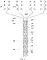
- Fig. 3 is a circuit connection diagram showing a first test circuit and a multiplexer according to an embodiment of the present disclosure.
- the first test sub-circuit 221 comprises a first transistor T1 and a second transistor T2.
- a first electrode of the first transistor T1 is configured to receive a first data signal S CTD1 .
- a second electrode of the first transistor T1 is electrically connected to an input terminal of the first multiplexer 241.
- a control electrode of the first transistor T1 is configured to receive a first test switch signal S CTSW1 .
- a first electrode of the second transistor T2 is configured to receive a second data signal S CTD2 .
- a second electrode of the second transistor T2 is electrically connected to an input terminal of the second multiplexer 242.
- a control electrode of the second transistor T2 is configured to receive a second test switch signal S CTSW2 .
- the second test sub-circuit 222 comprises a third transistor T3 and a fourth transistor T4.
- a first electrode of the third transistor T3 is configured to receive a third data signal S CTD3 .
- a second electrode of the third transistor T3 is electrically connected to the input terminal of the first multiplexer 241.
- a control electrode of the third transistor T3 is configured to receive a third test switch signal S CTSW3 .
- a first electrode of the fourth transistor T4 is configured to receive a fourth data signal S CTD4 .
- a second electrode of the fourth transistor T4 is electrically connected to the input terminal of the first multiplexer 241.
- a control electrode of the fourth transistor T4 is configured to receive a fourth test switch signal S CTSW4 .
- the third test sub-circuit 223 comprises a fifth transistor T5 and a sixth transistor T6.
- a first electrode of the fifth transistor T5 is configured to receive a fifth data signal S CTD5 .
- a second electrode of the fifth transistor T5 is electrically connected to the input terminal of the second multiplexer 242.
- a control electrode of the fifth transistor T5 is configured to receive a fifth test switch signal S CTSW5 .
- a first electrode of the sixth transistor T6 is configured to receive a sixth data signal S CTD6 .
- a second electrode of the sixth transistor T6 is electrically connected to the input terminal of the second multiplexer 242.
- a control electrode of the sixth transistor T6 is configured to receive a sixth test switch signal S CTSW6 .
- the fifth test switch signal S CTSW5 is the same as the third test switch signal S CTSW3
- the sixth test switch signal S CTSW6 is the same as the fourth test switch signal S CTSW4 .
- each multiplexer comprises a seventh transistor and an eighth transistor.
- the first multiplexer 241 comprises a seventh transistor T7 and an eighth transistor T8, and the second multiplexer 242 comprises a seventh transistor T7' and an eighth transistor T8'.
- the seventh transistor T7 and the eighth transistor T8 share a first electrode serving as the input terminal of the multiplexer.
- a second electrode of the seventh transistor T7 is electrically connected to one of the at least two signal transmission lines.
- the one of the at least two signal transmission lines is electrically connected to a column of sub-pixels in which red sub-pixels R and blue sub-pixels B are alternately arranged.
- a control electrode of the seventh transistor T7 is configured to receive a first selection signal S MUX1 .
- a second electrode of the eighth transistor T8 is electrically connected to another of the at least two signal transmission lines.
- the another of the at least two signal transmission lines is electrically connected to a column of green sub-pixels G.
- a control electrode of the eighth transistor T8 is configured to receive a second selection signal S MUX2 .
- the first to eighth transistors are all PMOS (positive channel Metal Oxide Semiconductor) transistors.
- the scope of the embodiments of the present disclosure is not limited to this.
- the first to the eighth transistors may also be NMOS (Negative channel Metal Oxide Semiconductor) transistors.
- test switch signals, data signals, and selection signals described above the various test sub-circuits and multiplexers can be controlled to implement a display test of the display panel.
- FIG. 4 is a timing diagram showing switch signals according to some embodiments of the present disclosure. A testing process of the display panel according to some embodiments of the present disclosure will be described in detail below in conjunction with FIG. 3 and FIG. 4 .
- the GCK signal and the GCB signal are clock control signals of a gate driving circuit.
- the GCK, GCB, and other signals are input to the gate driving circuit, so that the gate driving circuit outputs a gate control signal Gout(i) or Gout(i+1), wherein i is a positive integer.
- the gate driving circuit drives a pixel driving circuit of the sub-pixel in row scanning.
- the description will be given with an example in which the first to eighth transistors are PMOS transistors.
- the following method can be performed.
- the Gout(i) signal is at a low level, which enables the gate driving circuit in the i-th row; and the Gout(i+1) signal is at a high level, which disables the gate driving circuit in the (i+1)th row.
- i is a positive integer.
- the seventh transistors T7 and T7' are turned on when the first selection signal S MUX1 is at a low level.
- the third test switch signal S CTSW3 and the fifth test switch signal S CTSW5 are both at a low level, resulting in that the third transistor T3 and the fifth transistor T5 are also turned on.
- the third data signal SCTD3 can be input to the red sub-pixels R in the i-th row
- the fifth data signal S CTD5 can be input to the blue sub-pixels B in the i-th row.
- the third data signal S CTD3 is a data signal that makes the red sub-pixels emit light
- the fifth data signal S CTD5 is a data signal that cannot make the blue sub-pixels emit light. In this way, the red sub-pixels in the i-th row emit light, while the blue sub-pixels in the i-th row do not emit light.
- all the first selection signal S MUX1, the third test switch signal S CTSW3 , and the fifth test switch signal S CTSW5 change from a low level to a high level, resulting in that all the seventh transistors T7 and T7', the third transistor T3 and the fifth transistor T5 are turned off.
- the second selection signal S MUX2 changes from a high level to a low level, causing that the eighth transistors T8 and T8' are turned on.
- both the first test switch signal S CTSW1 and the second test switch signal S CTSW2 change to a low level, causing that both the first transistor T1 and the second transistor T2 are turned on.
- both the first data signal S CTD1 and the second data signal S CTD2 are input to the green sub-pixels G in the i-th row.
- both the first data signal S CTD1 and the second data signal S CTD2 are data signals that cannot cause the green sub-pixels to emit light, so that the green sub-pixels in the i-th row do not emit light.
- the Gout(i) signal changes from a low level to a high level, causing that the gate driving circuit in the i-th row is disabled.
- the Gout (i+1) signal changes from a high level to a low level, causing that the gate driving circuit in the (i+1)th row is enabled.
- the seventh transistors T7 and T7' are turned on when the first selection signal S MUX1 is at a low level.
- the fourth test switch signal S CTSW4 and the sixth test switch signal are both at a low level, causing that the fourth transistor T4 and the sixth transistor T6 are turned on.
- the fourth data signal S CTD4 is input to the blue sub-pixels B in the (i+1)th row
- the sixth data signal S CTD6 is input to the red sub-pixels R in the (i+1)th row.
- the fourth data signal S CTD4 is a data signal that cannot make the blue sub-pixels emit light
- the sixth data signal S CTD6 is a data signal that makes the red sub-pixels emit light. In this way, the red sub-pixels in the (i+1) th row emit light, while the blue sub-pixels in the (i+1)th row do not emit light.
- all the first selection signal S MUX1 , the fourth test switch signal S CTSW4 , and the sixth test switch signal change from a low level to a high level, resulting in that all the seventh transistors T7 and T7', the fourth transistor T4 and the sixth transistor T6 are turned off.
- the second selection signal S MUX2 changes from a high level to a low level, causing that the eighth transistors T8 and T8' are turned on.
- both the first test switch signal S CTSW1 and the second test switch signal S CTSW2 change to a low level, causing that both the first transistor T1 and the second transistor T2 are turned on.
- both the first data signal S CTD1 and the second data signal S CTD2 are input to the green sub-pixels G in the (i+1)th row.
- both the first data signal S CTD1 and the second data signal S CTD2 are data signals that cannot cause the green sub-pixels to emit light, so that the green sub-pixels in the (i+1)th row do not emit light.
- a method similar to the above method can be performed. The difference is that: in the process of displaying a blue screen as needed, the data signals (comprising the fourth data signal S CTD4 and the fifth data signal S CTD5 ) input to all the blue sub-pixels are signals that can make the blue sub-pixels emit light, the data signals (comprising the third data signal S CTD3 and the sixth data signal S CTD6 ) input to the red sub-pixels are data signals that cannot make the red sub-pixels emit light, and the data signals (comprising the first data signal S CTD1 and the second data signal S CTD2 ) input to the green sub-pixels are data signals that cannot make the green sub-pixels emit light. Therefore, the display panel can display the blue screen.
- the data signals (comprising the first data signal S CTD1 and the second data signal S CTD2 ) input to all the green sub-pixels are signals that can make the green sub-pixels emit light
- the data signals (comprising the third data signal S CTD3 and the sixth data signal S CTD6 ) input to the red sub-pixels are data signal that cannot make the red sub-pixels emit light
- the data signals (comprising the fourth data signal S CTD4 and the fifth data signal S CTD5 ) input to the blue sub-pixels are data signals that cannot make the blue sub-pixels emit light. Therefore, the display panel can display the green screen.
- each test component transmits a data signal to a multiplexer electrically connected to the test component under the control of a test switch signal; and the multiplexer transmits the data signal to corresponding sub-pixels under the control of a selection signal. This makes it easier to test the display panel.
- FIG. 5 is an enlarged schematic diagram showing a first test sub-circuit 221 in FIG. 2 according to an embodiment of the present disclosure.
- an orthographic projection of the first test sub-circuit on the base substrate is centrosymmetric. This may reduce the layout space of the first test circuit.
- the display panel further comprises a first control line LC1, a first data line LD1, and a second data line LD2.
- the first control line LC1 is electrically connected to a control electrode 510 of the first transistor T1 and a control electrode 520 of the second transistor T2.
- the first control line LC1 is electrically connected to the control electrode 510 of the first transistor T1 through a conductive via and a first connector 514; and the first control line LC1 is electrically connected to the control electrode 520 of the second transistor T2 through a conductive via and a second connector 524.
- the first control line LC1 is configured to transmit the first test switch signal S CTSW1 and the second test switch signal S CTSW2 .
- the first test switch signal is the same as the second test switch signal.
- the first data line LD1 is electrically connected to a first electrode 511 of the first transistor T1.
- the first data line LD1 is configured to transmit the first data signal S CTD1 .
- the second data line LD2 is electrically connected to a first electrode 521 of the second transistor T2.
- the second data line LD2 is configured to transmit the second data signal S CTD2 .
- An orthographic projection of the first control line LC1 on the base substrate is between an orthographic projection of the first data line LD1 on the base substrate and an orthographic projection of the second data line LD2 on the base substrate.
- FIG. 5 also shows a first active layer 513 of the first transistor T1 and a second active layer 523 of the second transistor T2.
- a second electrode 512 of the first transistor T1 is electrically connected to the first connection wire 2011.
- the second electrode 512 of the first transistor T1 is electrically connected to the first connection wire 2011 through a conductive via.
- a second electrode 522 of the second transistor T2 is electrically connected to the second connection wire 2012.
- the second electrode 522 of the second transistor T2 is electrically connected to the second connection wire 2012 through a conductive via (which will be described later).
- an orthographic projection of the control electrode 510 of the first transistor T1 on the base substrate is between an orthographic projection of the first electrode 511 of the first transistor T1 on the base substrate and an orthographic projection of the second electrode 512 of the first transistor T1 on the base substrate.
- An orthographic projection of the control electrode 520 of the second transistor T2 on the base substrate is between an orthographic projection of the first electrode 521 of the second transistor T2 on the base substrate and an orthographic projection of the second electrode 522 of the second transistor T2 on the base substrate.
- the orthographic projection of the first electrode 511 of the first transistor T1 on the base substrate and the orthographic projection of the first electrode 521 of the second transistor T2 on the base substrate are between the orthographic projection of the control electrode 510 of the first transistor T1 on the base substrate and the orthographic projection of the control electrode 520 of the second transistor T2 on the base substrate.
- FIG. 6 is an enlarged schematic diagram showing a second test sub-circuit 222 in FIG. 2 according to an embodiment of the present disclosure.
- the third transistor T3 comprises two first electrodes 5311 and 5312, one second electrode 532, and two control electrodes 5301 and 5302.
- the fourth transistor T4 comprises two first electrodes 5411 and 5412, one second electrode 542, and two control electrodes 5401 and 5402.
- FIG. 6 also shows a third active layer 533 of the third transistor T3 and a fourth active layer 543 of the fourth transistor T4.
- the third active layer 533 comprises a first sub-active layer 5331 and a second sub-active layer 5332
- the fourth active layer 543 comprises a third sub-active layer 5431 and a fourth sub-active layer 5432.
- the display panel further comprises a second control line LC2, a third data line LD3, a fourth data line LD4, a third control line LC3, a fifth data line LD5, and a sixth data line LD6.
- the second control line LC2 is electrically connected to the two control electrodes 5301 and 5302 of the third transistor T3.
- the second control line LC2 is electrically connected to the two control electrodes 5301 and 5302 of the third transistor T3 through a third connector 534 and a conductive via.
- the second control line LC2 is configured to transmit the third test switch signal S CTSW3 .
- the third data line LD3 is electrically connected to one first electrode 5311 of the two first electrodes of the third transistor T3.
- the third data line LD3 is configured to transmit the third data signal S CTD3 .
- the fourth data line LD4 is electrically connected to the other first electrode 5312 of the two first electrodes of the third transistor T3.
- the fourth data line LD4 is configured to transmit the third data signal S CTD3 .
- the third control line LC3 is electrically connected to the two control electrodes 5401 and 5402 of the fourth transistor T4.
- the third control line LC3 is electrically connected to the two control electrodes 5401 and 5402 of the fourth transistor T4 through a fourth connector 544 and a conductive via.
- the third control line LC3 is configured to transmit the fourth test switch signal S CTSW4 .
- the fifth data line LD5 is electrically connected to one first electrode 5411 of the two first electrodes of the fourth transistor T4.
- the fifth data line LD5 is configured to transmit the fourth data signal S CTD4 .
- the sixth data line LD6 is electrically connected to the other first electrode 5412 of the two first electrodes of the fourth transistor T4.
- the sixth data line LD6 is configured to transmit the fourth data signal S CTD4 .
- an orthographic projection of the second control line LC2 on the base substrate is between an orthographic projection of the third control line LC3 on the base substrate and an orthographic projection of the sixth data line LD6 on the base substrate.
- the orthographic projection of the third control line LC3 on the base substrate is between the orthographic projection of the second control line LC2 on the base substrate and an orthographic projection of the third data line LD3 on the base substrate.
- the orthographic projection of the third data line LD3 on the base substrate and the orthographic projection of the sixth data line LD6 on the base substrate are between an orthographic projection of the third transistor T3 on the base substrate and an orthographic projection of the fourth transistor T4 on the base substrate.
- the second electrode 532 of the third transistor T3 and the second electrode 542 of the fourth transistor T4 are both electrically connected to the first connection wire 2011.
- the second electrode 532 of the third transistor T3 and the second electrode 542 of the fourth transistor T4 are electrically connected to the first connection wire 2011 through conductive vias (which will be described later), respectively.
- an orthographic projection of one control electrode 5301 of the two control electrodes of the third transistor T3 on the base substrate is between an orthographic projection of one first electrode 5311 of the two first electrodes of the third transistor T3 on the base substrate and an orthographic projection of the second electrode 532 of the third transistor T3 on the base substrate.
- An orthographic projection of the other control electrode 5302 of the two control electrodes of the third transistor T3 on the base substrate is between an orthographic projection of the other first electrode 5312 of the two first electrodes of the third transistor T3 on the base substrate and the orthographic projection of the second electrode 532 of the third transistor T3 on the base substrate.
- an orthographic projection of one control electrode 5401 of the two control electrodes of the fourth transistor T4 on the base substrate is between an orthographic projection of one first electrode 5411 of the two first electrodes of the fourth transistor T4 on the base substrate and an orthographic projection of the second electrode 542 of the fourth transistor T4 on the base substrate.
- An orthographic projection of the other control electrode 5402 of the two control electrodes of the fourth transistor T4 on the base substrate is between an orthographic projection of the other first electrode 5412 of the two first electrodes of the fourth transistor T4 on the base substrate and the orthographic projection of the second electrode 542 of the fourth transistor T4 on the base substrate.
- FIG. 7 is an enlarged schematic diagram showing a third test sub-circuit 223 in FIG. 2 according to an embodiment of the present disclosure.
- the fifth transistor T5 comprises two first electrodes 5511 and 5512, one second electrode 552, and two control electrodes 5501 and 5502.
- the sixth transistor T6 comprises two first electrodes 5611 and 5612, one second electrode 562, and two control electrodes 5601 and 5602.
- FIG. 7 further shows a fifth active layer 553 of the fifth transistor T5 and a sixth active layer 563 of the sixth transistor T6.
- the fifth active layer 553 comprises a fifth sub-active layer 5531 and a sixth sub-active layer 5532; and the sixth active layer 563 comprises a seventh sub-active layer 5631 and an eighth sub-active layer 5632.
- the display panel further comprises a fourth control line LC4, a seventh data line LD7, an eighth data line LD8, a fifth control line LC5, a ninth data line LD9, and a tenth data line LD10.
- the fourth control line LC4 is electrically connected to the two control electrodes 5501 and 5502 of the fifth transistor T5.
- the fourth control line LC4 is electrically connected to the two control electrodes 5501 and 5502 of the fifth transistor T5 through a fifth connector 554 and a conductive via.
- the fourth control line LC4 is configured to transmit the fifth test switch signal S CTSW5 .
- the seventh data line LD7 is electrically connected to one first electrode 5511 of the two first electrodes of the fifth transistor T5.
- the seventh data line LD7 is configured to transmit the fifth data signal S CTD5 .
- the eighth data line LD8 is electrically connected to the other first electrode 5512 of the two first electrodes of the fifth transistor T5.
- the eighth data line LD8 is configured to transmit the fifth data signal S CTD5 .
- the fifth control line LC5 is electrically connected to the two control electrodes 5601 and 5602 of the sixth transistor T6.
- the fifth control line LC5 is electrically connected to the two control electrodes 5601 and 5602 of the sixth transistor T6 through a sixth connector 564 and a conductive via.
- the fifth control line LC5 is configured to transmit the sixth test switch signal S CTSW6 .
- the ninth data line LD9 is electrically connected to one first electrode 5611 of the two first electrodes of the sixth transistor T6.
- the ninth data line LD9 is configured to transmit the sixth data signal S CTD6 .
- the tenth data line LD10 is electrically connected to the other first electrode 5612 of the two first electrodes of the sixth transistor T6.
- the tenth data line LD10 is configured to transmit the sixth data signal S CTD6 .
- an orthographic projection of the fourth control line LC4 on the base substrate is between an orthographic projection of the fifth control line LC5 on the base substrate and an orthographic projection of the ninth data line LD9 on the base substrate.
- the orthographic projection of the fifth control line LC5 on the base substrate is between the orthographic projection of the fourth control line LC4 on the base substrate and an orthographic projection of the seventh data line LD7 on the base substrate.
- the orthographic projection of the seventh data line LD7 on the base substrate and the orthographic projection of the ninth data line LD9 on the base substrate are between an orthographic projection of the fifth transistor T5 on the base substrate and an orthographic projection of the sixth transistor T6 on the base substrate.
- the second electrode 552 of the fifth transistor T5 and the second electrode 562 of the sixth transistor T6 are both electrically connected to the second connection wire 2012.
- the second electrode 552 of the fifth transistor T5 and the second electrode 562 of the sixth transistor T6 are electrically connected to the second connection wire 2012 through conductive vias (which will be described later), respectively.
- an orthographic projection of one control electrode 5501 of the two control electrodes of the fifth transistor T5 on the base substrate is between an orthographic projection of one first electrode 5511 of the two first electrodes of the fifth transistor T5 on the base substrate and an orthographic projection of the second electrode 552 of the fifth transistor T5 on the base substrate.
- An orthographic projection of the other control electrode 5502 of the two control electrodes of the fifth transistor T5 on the base substrate is between an orthographic projection of the other first electrode 5512 of the two first electrodes of the fifth transistor T5 on the base substrate and the orthographic projection of the second electrode 552 of the fifth transistor T5 on the base substrate.
- an orthographic projection of one control electrode 5601 of the two control electrodes of the sixth transistor T6 on the base substrate is between an orthographic projection of one first electrode 5611 of the two first electrodes of the sixth transistor T6 on the base substrate and an orthographic projection of the second electrode 562 of the sixth transistor T6 on the base substrate.
- An orthographic projection of the other control electrode 5602 of the two control electrodes of the sixth transistor T6 on the base substrate is between an orthographic projection of the other first electrode 5612 of the two first electrodes of the sixth transistor T6 on the base substrate and the orthographic projection of the second electrode 562 of the sixth transistor T6 on the base substrate.
- the layout diagram of the first transistor T1 to the sixth transistor T6 according to some embodiments of the present disclosure has been described.
- the above layout diagram is only exemplary, and the scope of the embodiments of the present disclosure is not limited to this.
- the positions of the third transistor T3 and the fourth transistor T4 can be interchanged, and the positions of the fifth transistor T5 and the sixth transistor T6 can also be interchanged.
- FIG. 8 is a schematic cross-sectional view showing a sub-pixel according to an embodiment of the present disclosure. As shown in FIG. 8 , at least one sub-pixel comprises a ninth transistor T9 and a capacitor C0.
- the ninth transistor T9 comprises an active layer (for example, it may be referred to as a seventh active layer) 802.
- the active layer 802 is on a buffer layer 801.
- the buffer layer 801 is on the base substrate 10.
- the active layer 802 comprises a semiconductor layer.
- a material of the active layer 802 comprises at least one of polysilicon or amorphous silicon.
- the ninth transistor T9 further comprises a first insulating layer 811 covering the active layer 802.
- the first insulating layer 811 is an inorganic insulating layer.
- a material of the first insulating layer 811 comprises silicon dioxide, silicon nitride, or the like.
- the ninth transistor T9 further comprises a gate 803 on a side of the first insulating layer 811 away from the active layer 802.
- a material of the gate 803 comprises metal such as molybdenum (Mo).
- the ninth transistor T9 further comprises a second insulating layer 812 covering the gate 803.
- the second insulating layer 812 is an inorganic insulating layer.
- a material of the second insulating layer 812 comprises silicon dioxide, silicon nitride, or the like.
- the ninth transistor T9 further comprises an interlayer insulating layer 815 on a side of the second insulating layer 812 away from the gate 803.
- the interlayer insulating layer 815 is an inorganic insulating layer.
- a material of the interlayer insulating layer 815 comprises silicon dioxide, silicon nitride, or the like.
- the ninth transistor T9 further comprises a source 804 and a drain 805 both on a side of the interlayer insulating layer 815 away from the second insulating layer 812.
- materials of the source 804 and the drain 805 comprise at least one of titanium (Ti) or aluminum (Al).
- the source 804 and the drain 805 each comprise a three-layer structure of Ti/Al/Ti.
- the source 804 and the drain 805 each are electrically connected to the active layer 802.
- the source 804 is electrically connected to the active layer 802 through a conductive via passing through the first insulating layer 811, the second insulating layer 812, and the interlayer insulating layer 815; and the drain 805 is electrically connected to the active layer 802 through another conductive via passing through the first insulating layer 811, the second insulating layer 812, and the interlayer insulating layer 815.
- the capacitor C0 comprises a first conductive layer 821 in the same layer as the gate 803.
- a material of the first conductive layer 821 may be the same as the material of the gate 803. This can facilitate the manufacture of the display panel.
- the first conductive layer 821 is covered by the second insulating layer 812.
- the capacitor C0 further comprises a second conductive layer 822 on a side of the second insulating layer 812 away from the first conductive layer 821.
- the second conductive layer 822 is covered by the interlayer insulating layer 815.
- both a material of the first conductive layer 821 and a material of the second conductive layer 822 comprise metal such as molybdenum.
- the capacitor C0 can be used for storing data.
- the "same layer" in this embodiment of the present disclosure may refer to film layers on the same structural layer.
- film layers in the same layer may be a layer structure formed by using the same film forming process to form a film layer for forming a specific pattern, and then using the same mask to pattern the film layer through a single patterning process.
- the single patterning process may comprise multiple exposure, development or etching processes, and the particular patterns in the formed layer structure may or may not be continuous. These particular patterns may also be at different heights or have different thicknesses.
- the first conductive layer 821 is in the same layer as the gate 803.
- the first conductive layer 821 and the gate 803 are both on the first insulating layer 811.
- the first conductive layer 821 and the gate 803 can be formed in the same patterning process.
- the sub-pixel further comprises a third insulating layer 813 covering the source 804 and the drain 805.
- a material of the third insulating layer 813 comprises silicon dioxide, silicon nitride, or the like.
- the sub-pixel further comprises a planarization layer 817 on a side of the third insulating layer 813 away from the source 804 and the drain 805.
- a material of the planarization layer 817 comprises an organic insulating material.
- the sub-pixel further comprises an anode layer 831 on a side of the planarization layer 817 away from the third insulating layer 813.
- the anode layer 831 is electrically connected to the source 804 or the drain 805.
- the anode layer 831 is electrically connected to the drain 805 through a conductive via passing through the planarization layer 817 and the third insulating layer 813.
- the sub-pixel further comprises a pixel defining layer 840 on a side of the planarization layer 817 away from the third insulating layer 813 and having an opening 8401.
- the opening 8401 exposes at least a portion of the anode layer 831.
- the sub-pixel further comprises a functional layer 832 at least within the opening 8401 and connected to the anode layer 831.
- the functional layer 832 comprises a light-emitting layer or the like.
- the sub-pixel may further comprises a spacer layer 819 on a side of the pixel defining layer 840 away from the planarization layer 817.
- a material of the spacer layer 819 comprises an inorganic insulating material or an organic insulating material.
- the sub-pixel further comprises a cathode layer 833 on a side of the functional layer 832 away from the anode layer 831.
- the cathode layer 833 may cover the spacer layer 819 and the functional layer 832.
- a light emitting device comprises the anode layer 831, the functional layer 832, and the cathode layer 833.
- the sub-pixel further comprises an encapsulation layer on a side of the cathode layer 833 away from the functional layer 832.
- the encapsulation layer comprises a first inorganic encapsulation layer 851 covering the cathode layer, an organic encapsulation layer 850 on a side of the first inorganic encapsulation layer 851 away from the cathode layer 833, and a second inorganic encapsulation layer 852 on a side of the organic encapsulation layer 850 away from the first inorganic encapsulation layer 851.
- the first connection wire 2011 is in the same layer as the second conductive layer 822, and the second connection wire 2012 is in the same layer as the gate 803. In other embodiments, the first connection wire 2011 is in the same layer as the gate 803, and the second connection wire 2012 is in the same layer as the second conductive layer 822.
- the first control line LC1 to the fifth control line LC5 and the first data line LD1 to the tenth data line LD10 are all in the same layer as the source 804 or the drain 805.
- control electrodes of the first transistor T1 to the sixth transistor T6 are in the same layer as the gate 803.
- the active layers of the first transistor T1 to the sixth transistor T6 are in the same layer as the active layer 802 of the ninth transistor T9.
- the first electrodes of the first transistor T1 to the sixth transistor T6 are all in the same layer as the source 804 or the drain 805.
- the second electrodes of the first transistor T1 to the sixth transistor T6 are all in the same layer as the source 804 or the drain 805.
- FIG. 9 is a cross-sectional view showing a structure of a first test sub-circuit taken along the line A-A' in FIG. 5 according to an embodiment of the present disclosure.
- the first electrode 521 and the second electrode 522 of the second transistor T2 are on the interlayer insulating layer 815.
- the first electrode 521 of the second transistor T2 is electrically connected to the second active layer 523 through a first conductive via V1.
- the second electrode 522 of the second transistor T2 is electrically connected to the second active layer 523 through a second conductive via V2.
- the second electrode 522 of the second transistor T2 is also electrically connected to the second connection wire 2012 through a third conductive via V3.
- the control electrode 520 of the second transistor T2 is in the same layer as the second connection wire 2012.
- the structure of the first transistor T1 is substantially similar to the structure of the second transistor T2, and will not be described in detail here. Compared with the structure of the second transistor T2, the structure of the first transistor T1 differs in that the second electrode 512 of the first transistor T1 is electrically connected to the first connection wire 2011 through a conductive via.
- FIG. 10 is a cross-sectional view showing a structure of a second test sub-circuit taken along the line B-B' in FIG. 6 according to an embodiment of the present disclosure.
- first electrodes 5311 and 5312 and one second electrode 532 of the third transistor T3 are on the interlayer insulating layer 815.
- one first electrode 5311 of the third transistor T3 is electrically connected to the first sub-active layer 5331 through a fourth conductive via V4.
- the other first electrode 5312 of the third transistor T3 is electrically connected to the second sub-active layer 5332 through a fifth conductive via V5.
- the second electrode 532 of the third transistor T3 is electrically connected to the first sub-active layer 5331 through a sixth conductive via V6.
- the second electrode 532 of the third transistor T3 is also electrically connected to the second sub-active layer 5332 through a seventh conductive via V7.
- the second electrode 532 of the third transistor T3 is also electrically connected to the first connection wire 2011 through an eighth conductive via V8 and a ninth conductive via V9.
- the first connection wire 2011 is in the same layer as the second conductive layer 822.
- the structure of the fourth transistor T4 is similar to the structure of the third transistor T3, and will not be described in detail here.
- FIG. 11 is a cross-sectional view showing a structure of a third test sub-circuit taken along the line C-C' in FIG. 7 according to an embodiment of the present disclosure.
- two first electrodes 5511 and 5512 and one second electrode 552 of the fifth transistor T5 are on the interlayer insulating layer 815.
- one first electrode 5511 of the fifth transistor T5 is electrically connected to the fifth sub-active layer 5531 through a tenth conductive via V10.
- the other first electrode 5512 of the fifth transistor T5 is electrically connected to the sixth sub-active layer 5532 through an eleventh conductive via V11.
- the second electrode 552 of the fifth transistor T5 is electrically connected to the fifth sub-active layer 5531 through a twelfth conductive via V12.
- the second electrode 552 of the fifth transistor T5 is also electrically connected to the sixth sub-active layer 5532 through a thirteenth conductive via V13.
- the second electrode 552 of the fifth transistor T5 is also electrically connected to the second connection wire 2012 through a fourteenth conductive via V14 and a fifteenth conductive via V15.
- the second connection wire 2012 is in the same layer as the gate 803.
- the structure of the sixth transistor T6 is similar to the structure of the fifth transistor T5, and will not be described in detail here.
- FIG. 12 is a schematic diagram showing a layout of a multiplexer according to an embodiment of the present disclosure.
- the seventh transistor T7 and the eighth transistor T8 are shown in FIG. 12 .
- the seventh transistor T7 (or the eighth transistor T8) comprises an active layer (it may be referred to as an eighth active layer) 2321, a gate 2322, two first electrodes 2323, and a second electrode 2324.
- the seventh transistor T7 and the eighth transistor T8 share one first electrode 2323, which can reduce the space occupied by the multiplexer.
- This first electrode 2323 is electrically connected to the first connection wire 2011.
- the power bus 38 is also shown in FIG. 12 .
- the gate 2322 comprises a first gate portion 2322a and a second gate portion 2322b that are spaced apart from each other.
- the first gate portion 2322a and the second gate portion 2322b are electrically connected to one of a plurality of control signal lines 36.
- the second electrode 2324 is electrically connected to one transmission line 202.
- An orthographic projection of the second electrode 2324 on the base substrate is between the orthographic projections of the two first electrodes 2323 on the base substrate.
- the second electrode 2324 is in the same layer as the first electrodes 2323.
- the seventh transistor T7 (or the eighth transistor T8) further comprises at least one of an electrode connection portion 2325 or a gate connection portion 2326.
- the two first electrodes 2323 and the electrode connection portion 2325 are integrally provided.
- the first gate portion 2322a, the second gate portion 2322b, and the gate connection portion 2326 are integrally provided.
- An orthographic projection of the electrode connection portion 2325 on the base substrate is between an orthographic projection of the active layer 2321 on the base substrate and an orthographic projection of the plurality of control signal lines 36 on the base substrate.
- the two first electrodes 2323 are electrically connected to the first connection wire 2011 via the electrode connection portion 2325.
- An orthographic projection of the gate connection portion 2326 on the base substrate is between an orthographic projection of the active layer 2321 on the base substrate and an orthographic projection of the electrode connection portion 2325 on the base substrate.
- the first gate portion 2322a and the second gate portion 2322b are electrically connected to one control signal line 36 via the gate connection portion 2326.
- the seventh transistor T7 (or the eighth transistor T8) further comprises at least one of the electrode connection portion 2325 or the gate connection portion 2326.
- Such a structure facilitates the electrical connection between the first connection wire 2011 and the first electrode 2323, and the electrical connection between the control signal line 36 and the gate 2322.
- an orthographic projection of the first gate portion 2322a on the base substrate is between an orthographic projection of one of the two first electrodes 2323 on the base substrate and an orthographic projection of the second electrode 2324 on the base substrate
- an orthographic projection of the second gate portion 2322b on the base substrate is between an orthographic projection of the other of the two first electrodes 2323 on the base substrate and the orthographic projection of the second electrode 2324 on the base substrate.
- the active layer 2321 comprises a first active portion 2321a and a second active portion 2321b spaced apart from each other.
- the second active portion 2321b is between the first active portion 2321a and the display area.
- Each first electrode 2323 and the second electrode 2324 each are electrically connected to the first active portion 2321a through a plurality of sixteenth conductive vias V16, and the each first electrode 2323 and the second electrode 2324 each are electrically connected to the second active portion 2321b through a plurality of seventeenth conductive vias V17.
- the active layer 2321 comprises a first active portion 2321a and a second active portion 2321b spaced apart from each other. Such a structure is conducive to the heat dissipation of the transistors and can improve the reliability of the multiplexer.
- FIG. 13 is a top view showing a layout of a first test circuit and a second test circuit according to an embodiment of the present disclosure.
- FIG. 14 is a circuit connection diagram showing a second test circuit according to an embodiment of the present disclosure.
- the display panel further comprises a second test circuit 701.
- the second test circuit 701 is on a side of the first test circuit away from the plurality of sub-pixels.
- the second test circuit is configured to detect whether there is a crack in the display panel.
- the second test circuit 701 comprises a plurality of tenth transistors T10 and T10'.
- the plurality of tenth transistors are electrically connected to the plurality of multiplexers in one-to-one correspondence.
- a first electrode of the tenth transistor T10 (or T10') is configured to receive a detection voltage signal S CTD7 (or S' CTD7 ) .
- a second electrode of the tenth transistor T10 (or T10') is electrically connected to the input terminal of a multiplexer corresponding to the tenth transistor.
- a control electrode of the tenth transistor T10 (or T10') is configured to receive a seventh test switch signal S CTSW7 .
- FIG. 15 is a schematic diagram showing a detection principle of a second test circuit according to an embodiment of the present disclosure.
- the display panel further comprises a first detection line LT1 electrically connected to the first electrode of the tenth transistor T10 and a signal input terminal 610 electrically connected to the first detection line LT1.
- the signal input terminal 610 is used to output the detection voltage signal S CTD7 to the tenth transistor.
- the first detection line LT1 and the signal input terminal 610 are in the peripheral area 120.
- the principle of the second test circuit for detecting whether there is a crack in the display panel will be described below with reference to FIG. 11 .
- a description will be given with the transistors T7', T8', and T10' as an example.
- the seventh test switch signal is provided to the tenth transistor T10' to turn on the tenth transistor T10', and the detection voltage signal S' CTD7 (for example, at a high level) is provided to the tenth switch transistor T10'.
- the first selection signal S MUX1 is provided to the seventh transistor T7', and the second selection signal S MUX2 is provided to the eighth transistor T8'.
- the detection voltage signal S' CTD7 at a high level (for example, 6V) is input to corresponding sub-pixels through the tenth transistor T10' and the seventh transistor T7' (or the eighth transistor T8), so that the current flowing through the light emitting devices (such as OLED) of the sub-pixels is relatively small.
- the light emitting devices hardly emit light. In this way, the display panel displays a black screen. Therefore, if the display panel displays a black screen, it means that the display panel has no cracks.
- the first electrode of the tenth transistor T10' is suspended. It can be considered that the detection voltage signal in this case is approximately 0V. A voltage of 0V is input to the sub-pixels of a corresponding column through the tenth transistor T10' and the seventh transistor T7' (or the eighth transistor T8'), so that the current flowing through the light emitting devices of the column of sub-pixels is relatively large, causing that the light emitting devices emit light. Thus, the display panel shows a bright line.
- the seventh transistor and the eighth transistor cause the seventh transistor and the eighth transistor to be turned on alternately, if there is a crack in the display panel, all the red sub-pixels R, the green sub-pixels G, and the blue sub-pixels B emit light, which causes the display panel to display a white bright line. Therefore, in such a case, if the display panel displays a white bright line, it is determined that the display panel has a crack.
- the first selection signal turns off the seventh transistor and the second selection signal turns on the eighth transistor
- the green sub-pixels G emit light
- the red sub-pixels R and blue sub-pixels B do not emit light, causing that the display panel displays a green bright line. Therefore, in such a case, if the display panel displays a green bright line, it is determined that the display panel has a crack.
- the red sub-pixels R and the blue sub-pixels B emit light, while the green sub-pixels G do not emit light.
- the light emission of the red sub-pixels R and the blue sub-pixels B causes the display panel to display a magenta bright line. Therefore, in such a case, if the display panel displays a magenta bright line, it is determined that the display panel has a crack.
- the detection method is relatively simple and convenient for detection.
- FIG. 16 is a schematic top view showing a layout of a second test circuit according to an embodiment of the present disclosure.
- the second test circuit comprises a plurality of test components (for example, it may be referred to as second test components).
- Each second test component comprises two tenth transistors.
- a second test component 710 comprises two tenth transistors T10 and T10'.
- the tenth transistor T10 comprises a control electrode 10010, a first electrode 10011, and a second electrode 10012.
- the control electrode 10010 of the tenth transistor T10 is electrically connected to a sixth control line LC6 through a seventh connector 10014 and a conductive via.
- the sixth control line LC6 is configured to transmit the seventh test switch signal S CTSW7 .
- the first electrode 10011 of the tenth transistor T10 is electrically connected to a second detection line LT2.
- the second detection line LT2 is configured to transmit one detection voltage signal S CTD7 .
- the second electrode 10012 of the tenth transistor T10 is electrically connected to the first connection wire 2011.
- the tenth transistor T10' comprises a control electrode 10010', a first electrode 10011', and a second electrode 10012'.
- the control electrode 10010' of the tenth transistor T10' is electrically connected to the sixth control line LC6 through the seventh connector 10014 and a conductive via.
- the first electrode 10011' of the tenth transistor T10' is electrically connected to a first detection line LT1.
- the first detection line LT1 is configured to transmit another detection voltage signal S' CTD7 .
- the second electrode 10012' of the tenth transistor T10' is electrically connected to the second connection wire 2012.
- orthographic projections of the sixth control line LC6, the first detection line LT1 and the second detection line LT2 on the base substrate are between orthographic projections of the two tenth transistors T10 and T10' of the second test component on the base substrate.
- FIG. 16 also shows a third detection line LT3 and a fourth detection line LT4.
- the third detection line LT3 and the fourth detection line LT4 are each configured to provide detection voltage signals to the tenth transistors of other second test components.
- a display device comprises the display panel as described above.
- the display device may be any product or component with a display function, such as a mobile phone, a tablet computer, a television, a display, a notebook computer, a digital frame, a navigator, or the like.
- FIG. 17 is a flowchart showing a test method for a display panel according to an embodiment of the present disclosure. As shown in FIG. 17 , the test method comprises steps S1702 to S1704.
- a data signal is transmitted to a multiplexer electrically connected to each test component (that is, each test component of the first test circuit) by the each test component under the control of a test switch signal.
- the test switch signal comprises at least one of the first test switch signal to the sixth test switch signal.
- the data signal is transmitted to a corresponding sub-pixel by the multiplexer under the control of a selection signal.
- the selection signal comprises at least one of the first selection signal or the second selection signal.
- the test method comprises: transmitting a data signal to a multiplexer electrically connected to a test component of the first test circuit by the test component under a control of a test switch signal; and transmitting the data signal to a corresponding sub-pixel by the multiplexer under the control of a selection signal, thereby realizing the test of the display panel.
- FIG. 18 is a flowchart showing a crack detection method for a display panel according to an embodiment of the present disclosure. As shown in FIG. 18 , the crack detection method comprises steps S1802 to S1806.
- a detection voltage signal and a seventh test switch signal are provided to each tenth transistor.
- a first selection signal is provided to the seventh transistor, and a second selection signal is provided to the eighth transistor.
- step S1806 it is determined that the display panel has a crack in a case where the display panel displays a bright line.
- the step S1806 comprises: determining that the display panel has the crack if the display panel displays a white bright line in a case where the first selection signal and the second selection signal cause the seventh transistor and the eighth transistor to be turned on alternately; determining that the display panel has the crack if the display panel displays a green bright line in a case where the first selection signal turns off the seventh transistor and the second selection signal turns on the eighth transistor; or determining that the display panel has the crack if the display panel displays a magenta bright line in a case where the first selection signal turns on the seventh transistor and the second selection signal turns off the eighth transistor.
- the crack detection method comprises: providing the detection voltage signal and the seventh test switch signal to each tenth transistor; providing the first selection signal to the seventh transistor, and providing the second selection signal to the eighth transistor; and determining that the display panel has a crack in a case where the display panel displays a bright line. In this way, the crack detection of the display panel is realized.
Landscapes
- Engineering & Computer Science (AREA)
- Physics & Mathematics (AREA)
- Microelectronics & Electronic Packaging (AREA)
- Computer Hardware Design (AREA)
- General Physics & Mathematics (AREA)
- Theoretical Computer Science (AREA)
- Manufacturing & Machinery (AREA)
- Geometry (AREA)
- Devices For Indicating Variable Information By Combining Individual Elements (AREA)
- Control Of Indicators Other Than Cathode Ray Tubes (AREA)
Abstract
Description
- The present disclosure relates to the field of display technology, and in particular, to a display panel, a display device, a test method and a crack detection method.
- At present, multiplexers have been gradually applied to display screens, with the advantage of capable of reducing the number of data signal lines, thereby reducing costs . Multiplexers are usually located on a side of a test circuit away from a display area. In this way, the multiplexers are not enabled when a detection operation is performed by the test circuit. When the display modules are lighted up, the multiplexers can serve to transmit data signals.
- According to an aspect of embodiments of the present disclosure, a display panel is provided. The display panel comprises: a base substrate comprising a display area and a peripheral area on at least one side of the display area; a plurality of sub-pixels on a side of the base substrate and in the display area; a plurality of data signal lines in the display area and electrically connected to the plurality of sub-pixels; a plurality of signal transmission lines in the peripheral area and electrically connected to the plurality of data signal lines; a plurality of multiplexers in the peripheral area and on a side of the plurality of signal transmission lines away from the plurality of sub-pixels, at least one of the plurality of multiplexers being electrically connected to at least two signal transmission lines; and a first test circuit in the peripheral area and on a side of the plurality of multiplexers away from the plurality of sub-pixels, the first test circuit comprising a plurality of test components, each test component of at least a portion of the plurality of test components being electrically connected to at least two of the plurality of multiplexers, and the each test component comprising a first test sub-circuit, a second test sub-circuit and a third test sub-circuit, the second test sub-circuit being between the first test sub-circuit and the third test sub-circuit, and the first test sub-circuit being on a side of the second test sub-circuit away from the plurality of sub-pixels.
- In some embodiments, an orthographic projection of the first test sub-circuit on the base substrate is centrosymmetric.
- In some embodiments, two adjacent multiplexers of the plurality of multiplexers are electrically connected to one of the plurality of test components through two connection wires.
- In some embodiments, the plurality of multiplexers comprise a first multiplexer and a second multiplexer; the first test sub-circuit comprises: a first transistor, a first electrode of the first transistor being configured to receive a first data signal, a second electrode of the first transistor being electrically connected to an input terminal of the first multiplexer, and a control electrode of the first transistor being configured to receive a first test switch signal; and a second transistor, a first electrode of the second transistor being configured to receive a second data signal, a second electrode of the second transistor being electrically connected to an input terminal of the second multiplexer, and a control electrode of the second transistor being configured to receive a second test switch signal; the second test sub-circuit comprises: a third transistor, a first electrode of the third transistor being configured to receive a third data signal, a second electrode of the third transistor being electrically connected to the input terminal of the first multiplexer, and a control electrode of the third transistor being configured to receive a third test switch signal; and a fourth transistor, a first electrode of the fourth transistor being configured to receive a fourth data signal, a second electrode of the fourth transistor being electrically connected to the input terminal of the first multiplexer, and a control electrode of the fourth transistor being configured to receive a fourth test switch signal; and the third test sub-circuit comprises: a fifth transistor, a first electrode of the fifth transistor being configured to receive a fifth data signal, a second electrode of the fifth transistor being electrically connected to the input terminal of the second multiplexer, and a control electrode of the fifth transistor being configured to receive a fifth test switch signal; and a sixth transistor, a first electrode of the sixth transistor being configured to receive a sixth data signal, a second electrode of the sixth transistor being electrically connected to the input terminal of the second multiplexer, and a control electrode of the sixth transistor being configured to receive a sixth test switch signal.
- In some embodiments, the display panel further comprises: a first control line electrically connected to the control electrode of the first transistor and the control electrode of the second transistor and configured to transmit the first test switch signal and the second test switch signal, the first test switch signal being the same as the second test switch signal; a first data line electrically connected to the first electrode of the first transistor and configured to transmit the first data signal; and a second data line electrically connected to the first electrode of the second transistor and configured to transmit the second data signal; wherein an orthographic projection of the first control line on the base substrate is between an orthographic projection of the first data line on the base substrate and an orthographic projection of the second data line on the base substrate.
- In some embodiments, the two connection wires comprise a first connection wire and a second connection wire, wherein: the second electrode of the first transistor is electrically connected to the first connection wire, and the second electrode of the second transistor is electrically connected to the second connection wire; an orthographic projection of the control electrode of the first transistor on the base substrate is between an orthographic projection of the first electrode of the first transistor on the base substrate and an orthographic projection of the second electrode of the first transistor on the base substrate; an orthographic projection of the control electrode of the second transistor on the base substrate is between an orthographic projection of the first electrode of the second transistor on the base substrate and an orthographic projection of the second electrode of the second transistor on the base substrate; and the orthographic projection of the first electrode of the first transistor on the base substrate and the orthographic projection of the first electrode of the second transistor on the base substrate are between the orthographic projection of the control electrode of the first transistor on the base substrate and the orthographic projection of the control electrode of the second transistor on the base substrate.
- In some embodiments, he third transistor comprises two first electrodes, one second electrode, and two control electrodes; and the fourth transistor comprises two first electrodes, one second electrode, and two control electrodes; and the display panel further comprises: a second control line electrically connected to the two control electrodes of the third transistor and configured to transmit the third test switch signal; a third data line electrically connected to one of the two first electrodes of the third transistor and configured to transmit the third data signal; a fourth data line electrically connected to another of the two first electrodes of the third transistor and configured to transmit the third data signal; a third control line electrically connected to the two control electrodes of the fourth transistor and configured to transmit the fourth test switch signal; a fifth data line electrically connected to one of the two first electrodes of the fourth transistor and configured to transmit the fourth data signal; and a sixth data line electrically connected to another of the two first electrodes of the fourth transistor and configured to transmit the fourth data signal; wherein an orthographic projection of the second control line on the base substrate is between an orthographic projection of the third control line on the base substrate and an orthographic projection of the sixth data line on the base substrate, the orthographic projection of the third control line on the base substrate is between the orthographic projection of the second control line on the base substrate and an orthographic projection of the third data line on the base substrate, and the orthographic projection of the third data line on the base substrate and the orthographic projection of the sixth data line on the base substrate are between an orthographic projection of the third transistor on the base substrate and an orthographic projection of the fourth transistor on the base substrate.
- In some embodiments, the second electrode of the third transistor and the second electrode of the fourth transistor are electrically connected to the first connection wire; an orthographic projection of one of the two control electrodes of the third transistor on the base substrate is between an orthographic projection of the one of the two first electrodes of the third transistor on the base substrate and an orthographic projection of the second electrode of the third transistor on the base substrate, and an orthographic projection of another of the two control electrodes of the third transistor on the base substrate is between an orthographic projection of the another of the two first electrodes of the third transistor on the base substrate and the orthographic projection of the second electrode of the third transistor on the base substrate; and an orthographic projection of one of the two control electrodes of the fourth transistor on the base substrate is between an orthographic projection of the one of the two first electrodes of the fourth transistor on the base substrate and an orthographic projection of the second electrode of the fourth transistor on the base substrate, and an orthographic projection of another of the two control electrodes of the fourth transistor on the base substrate is between an orthographic projection of the another of the two first electrodes of the fourth transistor on the base substrate and the orthographic projection of the second electrode of the fourth transistor on the base substrate.
- In some embodiments, the fifth transistor comprises two first electrodes, one second electrode, and two control electrodes; and the sixth transistor comprises two first electrodes, one second electrode, and two control electrodes; the display panel further comprises: a fourth control line electrically connected to the two control electrodes of the fifth transistor and configured to transmit the fifth test switch signal; a seventh data line electrically connected to one of the two first electrodes of the fifth transistor and configured to transmit the fifth data signal; an eighth data line electrically connected to another of the two first electrodes of the fifth transistor and configured to transmit the fifth data signal; a fifth control line electrically connected to the two control electrodes of the sixth transistor and configured to transmit the sixth test switch signal; a ninth data line electrically connected to one of the two first electrodes of the sixth transistor and configured to transmit the sixth data signal; and a tenth data line electrically connected to another of the two first electrodes of the sixth transistor and configured to transmit the sixth data signal; wherein an orthographic projection of the fourth control line on the base substrate is between an orthographic projection of the fifth control line on the base substrate and an orthographic projection of the ninth data line on the base substrate, the orthographic projection of the fifth control line on the base substrate is between the orthographic projection of the fourth control line on the base substrate and an orthographic projection of the seventh data line on the base substrate, and the orthographic projection of the seventh data line on the base substrate and the orthographic projection of the ninth data line on the base substrate are between an orthographic projection of the fifth transistor on the base substrate and an orthographic projection of the sixth transistor on the base substrate.
- In some embodiments, the second electrode of the fifth transistor and the second electrode of the sixth transistor are electrically connected to the second connection wire; an orthographic projection of one of the two control electrodes of the fifth transistor on the base substrate is between an orthographic projection of the one of the two first electrodes of the fifth transistor on the base substrate and an orthographic projection of the second electrode of the fifth transistor on the base substrate, and an orthographic projection of another of the two control electrodes of the fifth transistor on the base substrate is between an orthographic projection of the another of the two first electrodes of the fifth transistor on the base substrate and the orthographic projection of the second electrode of the fifth transistor on the base substrate; and an orthographic projection of one of the two control electrodes of the sixth transistor on the base substrate is between an orthographic projection of the one of the two first electrodes of the sixth transistor on the base substrate and an orthographic projection of the second electrode of the sixth transistor on the base substrate, and an orthographic projection of another of the two control electrodes of the sixth transistor on the base substrate is between an orthographic projection of the another of the two first electrodes of the sixth transistor on the base substrate and the orthographic projection of the second electrode of the sixth transistor on the base substrate.
- In some embodiments, each of the plurality of multiplexers comprises a seventh transistor and an eighth transistor, wherein the seventh transistor and the eighth transistor share a first electrode serving as an input terminal of the each of the plurality of multiplexers, a second electrode of the seventh transistor is electrically connected to one of the at least two signal transmission lines, a control electrode of the seventh transistor is configured to receive a first selection signal, a second electrode of the eighth transistor is electrically connected to another of the at least two signal transmission lines, and a control electrode of the eighth transistor is configured to receive a second selection signal.
- In some embodiments, at least one sub-pixel of the plurality of sub-pixels comprises a ninth transistor and a capacitor; the ninth transistor comprising: an active layer; a first insulating layer covering the active layer; a gate on a side of the first insulating layer away from the active layer; a second insulating layer covering the gate; an interlayer insulating layer on a side of the second insulating layer away from the gate; and a source and a drain both on a side of the interlayer insulating layer away from the second insulating layer, wherein the source and the drain each are electrically connected to the active layer; and the capacitor comprising: a first conductive layer in the same layer as the gate and being covered by the second insulating layer; and a second conductive layer on a side of the second insulating layer away from the first conductive layer and being covered by the interlayer insulating layer.
- In some embodiments, the at least one sub-pixel further comprises: a third insulating layer covering the source and the drain; a planarization layer on a side of the third insulating layer away from the source and the drain; an anode layer on a side of the planarization layer away from the third insulating layer, wherein the anode layer is electrically connected to the source or the drain; a pixel defining layer on a side of the planarization layer away from the third insulating layer and having an opening exposing at least a portion of the anode layer; a functional layer at least within the opening and connected to the anode layer; and a cathode layer on a side of the functional layer away from the anode layer.
- In some embodiments, the first connection wire is in the same layer as the second conductive layer, and the second connection wire is in the same layer as the gate; the first control line to the fifth control line and the first data line to the tenth data line are all in the same layer as the source or the drain; and control electrodes of the first transistor to the sixth transistor are in the same layer as the gate, active layers of the first transistor to the sixth transistor are in the same layer as the active layer of the ninth transistor, first electrodes of the first transistor to the sixth transistor are all in the same layer as the source or the drain, and second electrodes of the first transistor to the sixth transistor are all in the same layer as the source or the drain.
- In some embodiments, the display panel further comprises: a second test circuit comprising a plurality of tenth transistors being electrically connected to the plurality of multiplexers in one-to-one correspondence; wherein a first electrode of each of the plurality of tenth transistors is configured to receive a detection voltage signal, a second electrode of the each of the plurality of tenth transistors is electrically connected to the input terminal of a multiplexer corresponding to the each of the plurality of tenth transistors, and a control electrode of the each of the plurality of tenth transistors is configured to receive a seventh test switch signal.
- In some embodiments, the display panel further comprises: a first signal access terminal group in the peripheral area and on a side of the first test circuit in an extension direction along a boundary between the display area and the peripheral area, the first signal access terminal group being electrically connected to the first test circuit; and a second signal access terminal group in the peripheral area and on a side of the first test circuit away from the first signal access terminal group in the extension direction along the boundary between the display area and the peripheral area, the second signal access terminal group being electrically connected to the first test circuit.
- According to another aspect of the embodiments of the present disclosure, a display device is provided. The display device comprising a display panel as described above.
- According to another aspect of the embodiments of the present disclosure, a test method for a display panel as described above is provided. The test method comprises: transmitting a data signal to a multiplexer electrically connected to the each test component by the each test component under a control of a test switch signal; and transmitting the data signal to a corresponding sub-pixel by the multiplexer under a control of a selection signal.
- According to another aspect of the embodiments of the present disclosure, a crack detection method for a display panel as described above is provided. The crack detection method comprises: providing the detection voltage signal and the seventh test switch signal to the each of the plurality of tenth transistors; providing the first selection signal to the seventh transistor and providing the second selection signal to the eighth transistor; and determining that the display panel has a crack in a case where the display panel displays a bright line.
- In some embodiments, the determining that the display panel has the crack comprises: determining that the display panel has the crack if the display panel displays a white bright line in a case where the first selection signal and the second selection signal cause the seventh transistor and the eighth transistor to be turned on alternately; determining that the display panel has the crack if the display panel displays a green bright line in a case where the first selection signal turns off the seventh transistor and the second selection signal turns on the eighth transistor; or determining that the display panel has the crack if the display panel displays a magenta bright line in a case where the first selection signal turns on the seventh transistor and the second selection signal turns off the eighth transistor.
- Other features and advantages of the present invention will become apparent from the following detailed description of exemplary embodiments of the present disclosure with reference to the accompanying drawings.
- The accompanying drawings, which constitute part of this specification, illustrate embodiments of the present disclosure and, together with this specification, serve to explain the principles of the present disclosure.
- The present disclosure may be more clearly understood from the following detailed description with reference to the accompanying drawings, in which:
-
FIG. 1A is a schematic top view showing a display panel according to an embodiment of the present disclosure; -
FIG. 1B is a schematic cross-sectional view showing a display panel according to an embodiment of the present disclosure; -
FIG. 2 is a top view showing a layout of a first test circuit according to an embodiment of the present disclosure; -
Fig. 3 is a circuit connection diagram showing a first test circuit and a multiplexer according to an embodiment of the present disclosure; -
FIG. 4 is a timing diagram showing switch signals according to some embodiments of the present disclosure; -
FIG. 5 is an enlarged schematic diagram showing afirst test sub-circuit 221 inFIG. 2 according to an embodiment of the present disclosure; -
FIG. 6 is an enlarged schematic diagram showing asecond test sub-circuit 222 inFIG. 2 according to an embodiment of the present disclosure; -
FIG. 7 is an enlarged schematic diagram showing athird test sub-circuit 223 inFIG. 2 according to an embodiment of the present disclosure; -
FIG. 8 is a schematic cross-sectional view showing a sub-pixel according to an embodiment of the present disclosure; -
FIG. 9 is a cross-sectional view showing a structure of a first test sub-circuit taken along the line A-A' inFIG. 5 according to an embodiment of the present disclosure; -
FIG. 10 is a cross-sectional view showing a structure of a second test sub-circuit taken along the line B-B' inFIG. 6 according to an embodiment of the present disclosure; -
FIG. 11 is a cross-sectional view showing a structure of a third test sub-circuit taken along the line C-C' inFIG. 7 according to an embodiment of the present disclosure; -
FIG. 12 is a schematic diagram showing a layout of a multiplexer according to an embodiment of the present disclosure; -
FIG. 13 is a top view showing a layout of a first test circuit and a second test circuit according to an embodiment of the present disclosure; -
FIG. 14 is a circuit connection diagram showing a second test circuit according to an embodiment of the present disclosure; -
FIG. 15 is a schematic diagram showing a detection principle of a second test circuit according to an embodiment of the present disclosure; -
FIG. 16 is a schematic top view showing a layout of a second test circuit according to an embodiment of the present disclosure; -
FIG. 17 is a flowchart showing a test method for a display panel according to an embodiment of the present disclosure; -
FIG. 18 is a flowchart showing a crack detection method for a display panel according to an embodiment of the present disclosure. - It should be understood that the dimensions of the various parts shown in the accompanying drawings are not drawn according to the actual scale. In addition, the same or similar reference signs are used to denote the same or similar components.
- Various exemplary embodiments of the present disclosure will now be described in detail in conjunction with the accompanying drawings. The description of the exemplary embodiments is merely illustrative and is in no way intended as a limitation to the present disclosure, its application or use. The present disclosure may be implemented in many different forms, which are not limited to the embodiments described herein. These embodiments are provided to make the present disclosure thorough and complete, and fully convey the scope of the present disclosure to those skilled in the art. It should be noticed that: relative arrangement of components and steps, material composition, numerical expressions, and numerical values set forth in these embodiments, unless specifically stated otherwise, should be explained as merely illustrative, and not as a limitation.
- The use of the terms "first", "second" and similar words in the present disclosure do not denote any order, quantity or importance, but are merely used to distinguish between different parts. A word such as "comprise", "include", or the like means that the element before the word covers the element(s) listed after the word without excluding the possibility of also covering other elements. The terms "up", "down", "left", "right", or the like are used only to represent a relative positional relationship, and the relative positional relationship may be changed correspondingly if the absolute position of the described object changes.
- In the present disclosure, when it is described that a particular device is located between the first device and the second device, there may be an intermediate device between the particular device and the first device or the second device, and alternatively, there may be no intermediate device. When it is described that a particular device is connected to other devices, the particular device may be directly connected to said other devices without an intermediate device, and alternatively, may not be directly connected to said other devices but with an intermediate device.
- All the terms (comprising technical and scientific terms) used in the present disclosure have the same meanings as understood by those skilled in the art of the present disclosure unless otherwise defined. It should also be understood that terms as defined in general dictionaries, unless explicitly defined herein, should be interpreted as having meanings that are consistent with their meanings in the context of the relevant art, and not to be interpreted in an idealized or extremely formalized sense.
- Techniques, methods, and apparatus known to those of ordinary skill in the relevant art may not be discussed in detail, but where appropriate, these techniques, methods, and apparatuses should be considered as part of this specification.
- The inventors of the present disclosure found that a multiplexer in the related art are usually located on a side of a test circuit away from a display area, and are on the same plane as an integrated circuit. During the process of lighting up the display modules, the multiplexer need to be switched frequently. For example, the multiplexer need to switch once in a time such as 4.17 microseconds or 5.3 microseconds. The high frequency switching of the multiplexers generates electromagnetic radiation in space. Since the multiplexer is close to the integrated circuit, the electromagnetic radiation generated by the multiplexer due to their high-frequency switching will cause electromagnetic interference on the integrated circuit, thereby affecting the operation of the integrated circuit.
- In view of this, embodiments of the present disclosure provide a display panel to reduce electromagnetic interference produced by the multiplexer on the integrated circuit.
-
FIG. 1A is a schematic top view showing a display panel according to an embodiment of the present disclosure.FIG. 2 is a top view showing a layout of a first test circuit according to an embodiment of the present disclosure. - As shown in
FIG. 1A , the display panel comprises: abase substrate 10, a plurality ofsub-pixels 101, a plurality of data signallines 102, a plurality ofsignal transmission lines 202, a plurality ofmultiplexers 240, and afirst test circuit 210. Thebase substrate 10 comprises adisplay area 110 and aperipheral area 120 on at least one side of thedisplay area 110. The plurality ofsub-pixels 101 are on a side of the base substrate and in thedisplay area 110. The plurality of data signallines 102 are in thedisplay area 110 and are electrically connected to the plurality ofsub-pixels 101. For example, the plurality of data signallines 102 are electrically connected to multiple columns ofsub-pixels 101 in one-to-one correspondence. The plurality ofsignal transmission lines 202 are in theperipheral area 120 and are electrically connected to the plurality of data signal lines 102. For example, the plurality ofsignal transmission lines 202 are electrically connected to the plurality of data signallines 102 in one-to-one correspondence. - The plurality of
multiplexers 240 are in the peripheral area and on a side of the plurality ofsignal transmission lines 202 away from the plurality ofsub-pixels 101. At least one of the plurality ofmultiplexers 240 is electrically connected to at least twosignal transmission lines 202. - As shown in
FIG. 1A , thefirst test circuit 210 is in theperipheral area 120 and on a side of the plurality ofmultiplexers 240 away from the plurality ofsub-pixels 101. Thefirst test circuit 210 comprises a plurality of test components (for example, they may be referred to as first test components) 214. Each test component of at least a portion of the plurality oftest components 214 is electrically connected to at least two of the plurality ofmultiplexers 240. For example, two adjacent multiplexers are electrically connected to one of the plurality of test components through twoconnection wires 201. - As shown in
FIG. 2 , eachtest component 214 comprises afirst test sub-circuit 221, asecond test sub-circuit 222 and athird test sub-circuit 223. Thesecond test sub-circuit 222 is between thefirst test sub-circuit 221 and thethird test sub-circuit 223. Thefirst test sub-circuit 221 is on a side of thesecond test sub-circuit 222 away from the plurality of sub-pixels. For example, as shown inFIG. 2 , an orthographic projection of thefirst test sub-circuit 221 on the base substrate is centrosymmetric. - Heretofore, a display panel according to some embodiments of the present disclosure is provided. In the display panel, the plurality of multiplexers are arranged between the first test circuit and the plurality of sub-pixels (or the display area). In this way, after bending the display panel, the multiplexers and the integrated circuit are on different planes, which can reduce electromagnetic interference produced by the multiplexers on the integrated circuit. Furthermore, the embodiment further provides the structure of the first test circuit. That is, the first test circuit comprises a plurality of test components . Each test component of at least a portion of the plurality of test components is electrically connected to at least two of the plurality of multiplexers. Each test component comprises a first test sub-circuit, a second test sub-circuit, and a third test sub-circuit. The second test sub-circuit is between the first test sub-circuit and the third test sub-circuit. The first test sub-circuit is on a side of the second test sub-circuit away from the plurality of sub-pixels.
- In some embodiments, as shown in
FIG. 1A , the display panel further comprises a first signalaccess terminal group 301 and a second signalaccess terminal group 302. The first signalaccess terminal group 301 is in theperipheral area 120. The first signalaccess terminal group 301 is on a side of thefirst test circuit 210 in an extending direction along a boundary between the display area and the peripheral area. For example, the first signalaccess terminal group 301 is electrically connected to thefirst test circuit 210 through lead wires. The first signalaccess terminal group 301 is configured to transmit test switch signals and data signals to thefirst test circuit 210. The second signalaccess terminal group 302 is in theperipheral area 120. The second signalaccess terminal group 302 is on a side of thefirst test circuit 210 away from the first signalaccess terminal group 301 in the extending direction along the boundary between the display area and the peripheral area. For example, the second signalaccess terminal group 302 is electrically connected to thefirst test circuit 210 through lead wires. The second signalaccess terminal group 302 is configured to transmit test switch signals and data signals to thefirst test circuit 210. This can realize the control of the first test circuit. - In some embodiments, as shown in
FIG. 1A , the display panel further comprise a plurality ofconnection pad areas 410, such as bond pad areas. The plurality ofconnection pad areas 410 are electrically connected to a plurality of data transmission lines. Each connection pad area is configured to transmit driving signals, such as data signals, to a plurality of sub-pixels. - In some embodiments, every two multiplexers are electrically connected to one
test component 214 through twoconnection wires 201. For example, as shown inFIG. 2 , the twoconnection wires 201 comprises afirst connection wire 2011 and asecond connection wire 2012. For example, as shown inFIG. 2 , the plurality ofmultiplexers 240 comprises afirst multiplexer 241 and asecond multiplexer 242. Thefirst multiplexer 241 is electrically connected to thetest component 214 through thefirst connection wire 2011, and thesecond multiplexer 242 is electrically connected to thetest component 214 through thesecond connection wire 2012. In this case, eachtest component 214 is electrically connected to at least foursignal transmission lines 202. -
FIG. 1B is a schematic cross-sectional view showing a display panel according to an embodiment of the present disclosure. In addition to thebase substrate 10, the sub-pixel 101, thesignal transmission line 202, themultiplexer 240, thefirst test circuit 210, and theconnection pad area 410, abending area 250 is also shown inFIG. 1B . It can be seen fromFIG. 1B that after bending the display panel, themultiplexer 240 and theconnection pad area 410 are on different planes. Theconnection pad area 410 may be electrically connected to an integrated circuit. Therefore, the above design may reduce electromagnetic interference produced by the multiplexer on the integrated circuit. - In some embodiments, as shown in
FIG. 2 , thefirst multiplexer 241 is electrically connected to two columns of sub-pixels. Thesecond multiplexer 242 is electrically connected to other two columns of sub-pixels. As shown inFIG. 2 , in the two columns of sub-pixels electrically connected to a multiplexer, one column of sub-pixels comprise red sub-pixels R and blue sub-pixels B that are alternately arranged, and the other column of sub-pixels comprises only green sub-pixels G. -
Fig. 3 is a circuit connection diagram showing a first test circuit and a multiplexer according to an embodiment of the present disclosure. - As shown in
FIG. 3 , thefirst test sub-circuit 221 comprises a first transistor T1 and a second transistor T2. A first electrode of the first transistor T1 is configured to receive a first data signal SCTD1. A second electrode of the first transistor T1 is electrically connected to an input terminal of thefirst multiplexer 241. A control electrode of the first transistor T1 is configured to receive a first test switch signal SCTSW1. A first electrode of the second transistor T2 is configured to receive a second data signal SCTD2. A second electrode of the second transistor T2 is electrically connected to an input terminal of thesecond multiplexer 242. A control electrode of the second transistor T2 is configured to receive a second test switch signal SCTSW2. - As shown in
FIG. 3 , thesecond test sub-circuit 222 comprises a third transistor T3 and a fourth transistor T4. A first electrode of the third transistor T3 is configured to receive a third data signal SCTD3. A second electrode of the third transistor T3 is electrically connected to the input terminal of thefirst multiplexer 241. A control electrode of the third transistor T3 is configured to receive a third test switch signal SCTSW3. A first electrode of the fourth transistor T4 is configured to receive a fourth data signal SCTD4. A second electrode of the fourth transistor T4 is electrically connected to the input terminal of thefirst multiplexer 241. A control electrode of the fourth transistor T4 is configured to receive a fourth test switch signal SCTSW4. - The
third test sub-circuit 223 comprises a fifth transistor T5 and a sixth transistor T6. A first electrode of the fifth transistor T5 is configured to receive a fifth data signal SCTD5. A second electrode of the fifth transistor T5 is electrically connected to the input terminal of thesecond multiplexer 242. A control electrode of the fifth transistor T5 is configured to receive a fifth test switch signal SCTSW5. A first electrode of the sixth transistor T6 is configured to receive a sixth data signal SCTD6. A second electrode of the sixth transistor T6 is electrically connected to the input terminal of thesecond multiplexer 242. A control electrode of the sixth transistor T6 is configured to receive a sixth test switch signal SCTSW6. - In some embodiments, the fifth test switch signal SCTSW5 is the same as the third test switch signal SCTSW3, and the sixth test switch signal SCTSW6 is the same as the fourth test switch signal SCTSW4.
- As shown in
FIG. 3 , each multiplexer comprises a seventh transistor and an eighth transistor. For example, thefirst multiplexer 241 comprises a seventh transistor T7 and an eighth transistor T8, and thesecond multiplexer 242 comprises a seventh transistor T7' and an eighth transistor T8'. - The following description will be given with the
first multiplexer 241 as an example. The seventh transistor T7 and the eighth transistor T8 share a first electrode serving as the input terminal of the multiplexer. A second electrode of the seventh transistor T7 is electrically connected to one of the at least two signal transmission lines. For example, the one of the at least two signal transmission lines is electrically connected to a column of sub-pixels in which red sub-pixels R and blue sub-pixels B are alternately arranged. A control electrode of the seventh transistor T7 is configured to receive a first selection signal SMUX1. A second electrode of the eighth transistor T8 is electrically connected to another of the at least two signal transmission lines. For example, the another of the at least two signal transmission lines is electrically connected to a column of green sub-pixels G. A control electrode of the eighth transistor T8 is configured to receive a second selection signal SMUX2. - In some embodiments, as shown in
FIG. 3 , the first to eighth transistors are all PMOS (positive channel Metal Oxide Semiconductor) transistors. Of course, the scope of the embodiments of the present disclosure is not limited to this. For example, the first to the eighth transistors may also be NMOS (Negative channel Metal Oxide Semiconductor) transistors. - In the embodiments of the present disclosure, with the test switch signals, data signals, and selection signals described above, the various test sub-circuits and multiplexers can be controlled to implement a display test of the display panel.
-
FIG. 4 is a timing diagram showing switch signals according to some embodiments of the present disclosure. A testing process of the display panel according to some embodiments of the present disclosure will be described in detail below in conjunction withFIG. 3 andFIG. 4 . - It should be noted that the GCK signal and the GCB signal are clock control signals of a gate driving circuit. The GCK, GCB, and other signals are input to the gate driving circuit, so that the gate driving circuit outputs a gate control signal Gout(i) or Gout(i+1), wherein i is a positive integer. In this way, the gate driving circuit drives a pixel driving circuit of the sub-pixel in row scanning. These signals are known to those skilled in the art and will not be described in detail here.
- Here, the description will be given with an example in which the first to eighth transistors are PMOS transistors.
- For example, in the case where a red screen needs to be displayed on the display panel for testing, the following method can be performed.
- As shown in
FIG. 4 , in a first stage t1, the Gout(i) signal is at a low level, which enables the gate driving circuit in the i-th row; and the Gout(i+1) signal is at a high level, which disables the gate driving circuit in the (i+1)th row. Here, i is a positive integer. - For example, in the first half of the first stage t1, the seventh transistors T7 and T7' are turned on when the first selection signal SMUX1 is at a low level. At this moment, the third test switch signal SCTSW3 and the fifth test switch signal SCTSW5 are both at a low level, resulting in that the third transistor T3 and the fifth transistor T5 are also turned on. In this way, the third data signal SCTD3 can be input to the red sub-pixels R in the i-th row, and the fifth data signal SCTD5 can be input to the blue sub-pixels B in the i-th row. In the process of displaying a red screen as needed, the third data signal SCTD3 is a data signal that makes the red sub-pixels emit light, and the fifth data signal SCTD5 is a data signal that cannot make the blue sub-pixels emit light. In this way, the red sub-pixels in the i-th row emit light, while the blue sub-pixels in the i-th row do not emit light.
- Next, in the second half of the first stage t1, all the first selection signal SMUX1, the third test switch signal SCTSW3, and the fifth test switch signal SCTSW5 change from a low level to a high level, resulting in that all the seventh transistors T7 and T7', the third transistor T3 and the fifth transistor T5 are turned off. The second selection signal SMUX2 changes from a high level to a low level, causing that the eighth transistors T8 and T8' are turned on. At this moment, both the first test switch signal SCTSW1 and the second test switch signal SCTSW2 change to a low level, causing that both the first transistor T1 and the second transistor T2 are turned on. Thus, the first data signal SCTD1 and the second data signal SCTD2 are input to the green sub-pixels G in the i-th row. However, in the process of displaying a red screen as needed, both the first data signal SCTD1 and the second data signal SCTD2 are data signals that cannot cause the green sub-pixels to emit light, so that the green sub-pixels in the i-th row do not emit light.
- Next, as shown in
FIG. 4 , in a second stage t2, the Gout(i) signal changes from a low level to a high level, causing that the gate driving circuit in the i-th row is disabled. The Gout (i+1) signal changes from a high level to a low level, causing that the gate driving circuit in the (i+1)th row is enabled. - For example, in the first half of the second stage t2, the seventh transistors T7 and T7' are turned on when the first selection signal SMUX1 is at a low level. At this moment, the fourth test switch signal SCTSW4 and the sixth test switch signal are both at a low level, causing that the fourth transistor T4 and the sixth transistor T6 are turned on. Thus, the fourth data signal SCTD4 is input to the blue sub-pixels B in the (i+1)th row, and the sixth data signal SCTD6 is input to the red sub-pixels R in the (i+1)th row. In the process of displaying a red screen as needed, the fourth data signal SCTD4 is a data signal that cannot make the blue sub-pixels emit light, and the sixth data signal SCTD6 is a data signal that makes the red sub-pixels emit light. In this way, the red sub-pixels in the (i+1) th row emit light, while the blue sub-pixels in the (i+1)th row do not emit light.
- Next, in the second half of the second stage t2, all the first selection signal SMUX1, the fourth test switch signal SCTSW4, and the sixth test switch signal change from a low level to a high level, resulting in that all the seventh transistors T7 and T7', the fourth transistor T4 and the sixth transistor T6 are turned off. The second selection signal SMUX2 changes from a high level to a low level, causing that the eighth transistors T8 and T8' are turned on. At this moment, both the first test switch signal SCTSW1 and the second test switch signal SCTSW2 change to a low level, causing that both the first transistor T1 and the second transistor T2 are turned on. Thus, the first data signal SCTD1 and the second data signal SCTD2 are input to the green sub-pixels G in the (i+1)th row. However, in the process of displaying a red screen as needed, both the first data signal SCTD1 and the second data signal SCTD2 are data signals that cannot cause the green sub-pixels to emit light, so that the green sub-pixels in the (i+1)th row do not emit light.
- Heretofore, the process of testing the red screen on the display panel has been described. In the process of displaying the red screen as needed, all the red sub-pixels of the display panel are inputted with data signals that make the red sub-pixels emit light. Although the blue sub-pixels and the green sub-pixels are also input with corresponding data signals, these data signals cannot make the blue sub-pixels and the green sub-pixels emit light, so that the red screen can be displayed during the test.
- In other embodiments, when a blue screen needs to be displayed on the display panel for testing, a method similar to the above method can be performed. The difference is that: in the process of displaying a blue screen as needed, the data signals (comprising the fourth data signal SCTD4 and the fifth data signal SCTD5) input to all the blue sub-pixels are signals that can make the blue sub-pixels emit light, the data signals (comprising the third data signal SCTD3 and the sixth data signal SCTD6) input to the red sub-pixels are data signals that cannot make the red sub-pixels emit light, and the data signals (comprising the first data signal SCTD1 and the second data signal SCTD2) input to the green sub-pixels are data signals that cannot make the green sub-pixels emit light. Therefore, the display panel can display the blue screen.
- In other embodiments, in the process of displaying a green screen as needed, the data signals (comprising the first data signal SCTD1 and the second data signal SCTD2) input to all the green sub-pixels are signals that can make the green sub-pixels emit light, the data signals (comprising the third data signal SCTD3 and the sixth data signal SCTD6) input to the red sub-pixels are data signal that cannot make the red sub-pixels emit light, and the data signals (comprising the fourth data signal SCTD4 and the fifth data signal SCTD5) input to the blue sub-pixels are data signals that cannot make the blue sub-pixels emit light. Therefore, the display panel can display the green screen.
- Heretofore, the test process of the display panel according to some embodiments of the present disclosure is realized. In this test process, each test component transmits a data signal to a multiplexer electrically connected to the test component under the control of a test switch signal; and the multiplexer transmits the data signal to corresponding sub-pixels under the control of a selection signal. This makes it easier to test the display panel.
-
FIG. 5 is an enlarged schematic diagram showing afirst test sub-circuit 221 inFIG. 2 according to an embodiment of the present disclosure. - In some embodiments, an orthographic projection of the first test sub-circuit on the base substrate is centrosymmetric. This may reduce the layout space of the first test circuit.
- In some embodiments, as shown in
FIGS. 2 and5 , the display panel further comprises a first control line LC1, a first data line LD1, and a second data line LD2. The first control line LC1 is electrically connected to acontrol electrode 510 of the first transistor T1 and acontrol electrode 520 of the second transistor T2. For example, the first control line LC1 is electrically connected to thecontrol electrode 510 of the first transistor T1 through a conductive via and afirst connector 514; and the first control line LC1 is electrically connected to thecontrol electrode 520 of the second transistor T2 through a conductive via and asecond connector 524. The first control line LC1 is configured to transmit the first test switch signal SCTSW1 and the second test switch signal SCTSW2. The first test switch signal is the same as the second test switch signal. The first data line LD1 is electrically connected to afirst electrode 511 of the first transistor T1. The first data line LD1 is configured to transmit the first data signal SCTD1. The second data line LD2 is electrically connected to afirst electrode 521 of the second transistor T2. The second data line LD2 is configured to transmit the second data signal SCTD2. An orthographic projection of the first control line LC1 on the base substrate is between an orthographic projection of the first data line LD1 on the base substrate and an orthographic projection of the second data line LD2 on the base substrate. In addition,FIG. 5 also shows a firstactive layer 513 of the first transistor T1 and a secondactive layer 523 of the second transistor T2. - As shown in
FIG. 5 , asecond electrode 512 of the first transistor T1 is electrically connected to thefirst connection wire 2011. Thesecond electrode 512 of the first transistor T1 is electrically connected to thefirst connection wire 2011 through a conductive via. Asecond electrode 522 of the second transistor T2 is electrically connected to thesecond connection wire 2012. For example, thesecond electrode 522 of the second transistor T2 is electrically connected to thesecond connection wire 2012 through a conductive via (which will be described later). - In some embodiments, an orthographic projection of the
control electrode 510 of the first transistor T1 on the base substrate is between an orthographic projection of thefirst electrode 511 of the first transistor T1 on the base substrate and an orthographic projection of thesecond electrode 512 of the first transistor T1 on the base substrate. An orthographic projection of thecontrol electrode 520 of the second transistor T2 on the base substrate is between an orthographic projection of thefirst electrode 521 of the second transistor T2 on the base substrate and an orthographic projection of thesecond electrode 522 of the second transistor T2 on the base substrate. The orthographic projection of thefirst electrode 511 of the first transistor T1 on the base substrate and the orthographic projection of thefirst electrode 521 of the second transistor T2 on the base substrate are between the orthographic projection of thecontrol electrode 510 of the first transistor T1 on the base substrate and the orthographic projection of thecontrol electrode 520 of the second transistor T2 on the base substrate. - Heretofore, the layout structure of the first test sub-circuit has been described.
-
FIG. 6 is an enlarged schematic diagram showing asecond test sub-circuit 222 inFIG. 2 according to an embodiment of the present disclosure. - In some embodiments, as shown in
FIG. 6 , the third transistor T3 comprises twofirst electrodes second electrode 532, and twocontrol electrodes first electrodes second electrode 542, and twocontrol electrodes FIG. 6 also shows a thirdactive layer 533 of the third transistor T3 and a fourthactive layer 543 of the fourth transistor T4. For example, the thirdactive layer 533 comprises a firstsub-active layer 5331 and a secondsub-active layer 5332, and the fourthactive layer 543 comprises a thirdsub-active layer 5431 and a fourthsub-active layer 5432. - In some embodiments, as shown in
FIG. 6 , the display panel further comprises a second control line LC2, a third data line LD3, a fourth data line LD4, a third control line LC3, a fifth data line LD5, and a sixth data line LD6. - The second control line LC2 is electrically connected to the two
control electrodes control electrodes third connector 534 and a conductive via. The second control line LC2 is configured to transmit the third test switch signal SCTSW3. - The third data line LD3 is electrically connected to one
first electrode 5311 of the two first electrodes of the third transistor T3. The third data line LD3 is configured to transmit the third data signal SCTD3. - The fourth data line LD4 is electrically connected to the other
first electrode 5312 of the two first electrodes of the third transistor T3. The fourth data line LD4 is configured to transmit the third data signal SCTD3. - The third control line LC3 is electrically connected to the two
control electrodes control electrodes fourth connector 544 and a conductive via. The third control line LC3 is configured to transmit the fourth test switch signal SCTSW4. - The fifth data line LD5 is electrically connected to one
first electrode 5411 of the two first electrodes of the fourth transistor T4. The fifth data line LD5 is configured to transmit the fourth data signal SCTD4. - The sixth data line LD6 is electrically connected to the other
first electrode 5412 of the two first electrodes of the fourth transistor T4. The sixth data line LD6 is configured to transmit the fourth data signal SCTD4. - In some embodiments, an orthographic projection of the second control line LC2 on the base substrate is between an orthographic projection of the third control line LC3 on the base substrate and an orthographic projection of the sixth data line LD6 on the base substrate. The orthographic projection of the third control line LC3 on the base substrate is between the orthographic projection of the second control line LC2 on the base substrate and an orthographic projection of the third data line LD3 on the base substrate. The orthographic projection of the third data line LD3 on the base substrate and the orthographic projection of the sixth data line LD6 on the base substrate are between an orthographic projection of the third transistor T3 on the base substrate and an orthographic projection of the fourth transistor T4 on the base substrate.
- As shown in
FIG. 6 , thesecond electrode 532 of the third transistor T3 and thesecond electrode 542 of the fourth transistor T4 are both electrically connected to thefirst connection wire 2011. For example, thesecond electrode 532 of the third transistor T3 and thesecond electrode 542 of the fourth transistor T4 are electrically connected to thefirst connection wire 2011 through conductive vias (which will be described later), respectively. - In some embodiments, an orthographic projection of one
control electrode 5301 of the two control electrodes of the third transistor T3 on the base substrate is between an orthographic projection of onefirst electrode 5311 of the two first electrodes of the third transistor T3 on the base substrate and an orthographic projection of thesecond electrode 532 of the third transistor T3 on the base substrate. An orthographic projection of theother control electrode 5302 of the two control electrodes of the third transistor T3 on the base substrate is between an orthographic projection of the otherfirst electrode 5312 of the two first electrodes of the third transistor T3 on the base substrate and the orthographic projection of thesecond electrode 532 of the third transistor T3 on the base substrate. - In some embodiments, an orthographic projection of one
control electrode 5401 of the two control electrodes of the fourth transistor T4 on the base substrate is between an orthographic projection of onefirst electrode 5411 of the two first electrodes of the fourth transistor T4 on the base substrate and an orthographic projection of thesecond electrode 542 of the fourth transistor T4 on the base substrate. An orthographic projection of theother control electrode 5402 of the two control electrodes of the fourth transistor T4 on the base substrate is between an orthographic projection of the otherfirst electrode 5412 of the two first electrodes of the fourth transistor T4 on the base substrate and the orthographic projection of thesecond electrode 542 of the fourth transistor T4 on the base substrate. -
FIG. 7 is an enlarged schematic diagram showing athird test sub-circuit 223 inFIG. 2 according to an embodiment of the present disclosure. - In some embodiments, as shown in
FIG. 7 , the fifth transistor T5 comprises twofirst electrodes second electrode 552, and twocontrol electrodes first electrodes second electrode 562, and twocontrol electrodes FIG. 7 further shows a fifthactive layer 553 of the fifth transistor T5 and a sixthactive layer 563 of the sixth transistor T6. For example, the fifthactive layer 553 comprises a fifthsub-active layer 5531 and a sixthsub-active layer 5532; and the sixthactive layer 563 comprises a seventhsub-active layer 5631 and an eighthsub-active layer 5632. - In some embodiments, as shown in
FIG. 7 , the display panel further comprises a fourth control line LC4, a seventh data line LD7, an eighth data line LD8, a fifth control line LC5, a ninth data line LD9, and a tenth data line LD10. - The fourth control line LC4 is electrically connected to the two
control electrodes control electrodes fifth connector 554 and a conductive via. The fourth control line LC4 is configured to transmit the fifth test switch signal SCTSW5. - The seventh data line LD7 is electrically connected to one
first electrode 5511 of the two first electrodes of the fifth transistor T5. The seventh data line LD7 is configured to transmit the fifth data signal SCTD5. - The eighth data line LD8 is electrically connected to the other
first electrode 5512 of the two first electrodes of the fifth transistor T5. The eighth data line LD8 is configured to transmit the fifth data signal SCTD5. - The fifth control line LC5 is electrically connected to the two
control electrodes control electrodes sixth connector 564 and a conductive via. The fifth control line LC5 is configured to transmit the sixth test switch signal SCTSW6. - The ninth data line LD9 is electrically connected to one
first electrode 5611 of the two first electrodes of the sixth transistor T6. The ninth data line LD9 is configured to transmit the sixth data signal SCTD6. - The tenth data line LD10 is electrically connected to the other
first electrode 5612 of the two first electrodes of the sixth transistor T6. The tenth data line LD10 is configured to transmit the sixth data signal SCTD6. - In some embodiments, an orthographic projection of the fourth control line LC4 on the base substrate is between an orthographic projection of the fifth control line LC5 on the base substrate and an orthographic projection of the ninth data line LD9 on the base substrate. The orthographic projection of the fifth control line LC5 on the base substrate is between the orthographic projection of the fourth control line LC4 on the base substrate and an orthographic projection of the seventh data line LD7 on the base substrate. The orthographic projection of the seventh data line LD7 on the base substrate and the orthographic projection of the ninth data line LD9 on the base substrate are between an orthographic projection of the fifth transistor T5 on the base substrate and an orthographic projection of the sixth transistor T6 on the base substrate.
- In some embodiments, as shown in
FIG. 7 , thesecond electrode 552 of the fifth transistor T5 and thesecond electrode 562 of the sixth transistor T6 are both electrically connected to thesecond connection wire 2012. For example, thesecond electrode 552 of the fifth transistor T5 and thesecond electrode 562 of the sixth transistor T6 are electrically connected to thesecond connection wire 2012 through conductive vias (which will be described later), respectively. - In some embodiments, an orthographic projection of one
control electrode 5501 of the two control electrodes of the fifth transistor T5 on the base substrate is between an orthographic projection of onefirst electrode 5511 of the two first electrodes of the fifth transistor T5 on the base substrate and an orthographic projection of thesecond electrode 552 of the fifth transistor T5 on the base substrate. An orthographic projection of theother control electrode 5502 of the two control electrodes of the fifth transistor T5 on the base substrate is between an orthographic projection of the otherfirst electrode 5512 of the two first electrodes of the fifth transistor T5 on the base substrate and the orthographic projection of thesecond electrode 552 of the fifth transistor T5 on the base substrate. - In some embodiments, an orthographic projection of one
control electrode 5601 of the two control electrodes of the sixth transistor T6 on the base substrate is between an orthographic projection of onefirst electrode 5611 of the two first electrodes of the sixth transistor T6 on the base substrate and an orthographic projection of thesecond electrode 562 of the sixth transistor T6 on the base substrate. An orthographic projection of theother control electrode 5602 of the two control electrodes of the sixth transistor T6 on the base substrate is between an orthographic projection of the otherfirst electrode 5612 of the two first electrodes of the sixth transistor T6 on the base substrate and the orthographic projection of thesecond electrode 562 of the sixth transistor T6 on the base substrate. - Heretofore, the layout diagram of the first transistor T1 to the sixth transistor T6 according to some embodiments of the present disclosure has been described. However, those skilled in the art can understand that the above layout diagram is only exemplary, and the scope of the embodiments of the present disclosure is not limited to this. For example, in the layout diagram, the positions of the third transistor T3 and the fourth transistor T4 can be interchanged, and the positions of the fifth transistor T5 and the sixth transistor T6 can also be interchanged.
-
FIG. 8 is a schematic cross-sectional view showing a sub-pixel according to an embodiment of the present disclosure. As shown inFIG. 8 , at least one sub-pixel comprises a ninth transistor T9 and a capacitor C0. - As shown in
FIG. 8 , the ninth transistor T9 comprises an active layer (for example, it may be referred to as a seventh active layer) 802. For example, theactive layer 802 is on abuffer layer 801. Thebuffer layer 801 is on thebase substrate 10. For example, theactive layer 802 comprises a semiconductor layer. For example, a material of theactive layer 802 comprises at least one of polysilicon or amorphous silicon. - As shown in
FIG. 8 , the ninth transistor T9 further comprises a first insulatinglayer 811 covering theactive layer 802. For example, the first insulatinglayer 811 is an inorganic insulating layer. For example, a material of the first insulatinglayer 811 comprises silicon dioxide, silicon nitride, or the like. - As shown in
FIG. 8 , the ninth transistor T9 further comprises agate 803 on a side of the first insulatinglayer 811 away from theactive layer 802. For example, a material of thegate 803 comprises metal such as molybdenum (Mo). - As shown in
FIG. 8 , the ninth transistor T9 further comprises a second insulatinglayer 812 covering thegate 803. For example, the second insulatinglayer 812 is an inorganic insulating layer. For example, a material of the second insulatinglayer 812 comprises silicon dioxide, silicon nitride, or the like. - As shown in
FIG. 8 , the ninth transistor T9 further comprises an interlayer insulatinglayer 815 on a side of the second insulatinglayer 812 away from thegate 803. For example, theinterlayer insulating layer 815 is an inorganic insulating layer. For example, a material of the interlayer insulatinglayer 815 comprises silicon dioxide, silicon nitride, or the like. - As shown in
FIG. 8 , the ninth transistor T9 further comprises asource 804 and adrain 805 both on a side of the interlayer insulatinglayer 815 away from the second insulatinglayer 812. For example, materials of thesource 804 and thedrain 805 comprise at least one of titanium (Ti) or aluminum (Al). For example, thesource 804 and thedrain 805 each comprise a three-layer structure of Ti/Al/Ti. Thesource 804 and thedrain 805 each are electrically connected to theactive layer 802. For example, thesource 804 is electrically connected to theactive layer 802 through a conductive via passing through the first insulatinglayer 811, the second insulatinglayer 812, and the interlayer insulatinglayer 815; and thedrain 805 is electrically connected to theactive layer 802 through another conductive via passing through the first insulatinglayer 811, the second insulatinglayer 812, and the interlayer insulatinglayer 815. - Heretofore, the ninth transistor for the sub-pixel according to some embodiments of the present disclosure has been described.
- In some embodiments, as shown in
FIG. 8 , the capacitor C0 comprises a firstconductive layer 821 in the same layer as thegate 803. For example, a material of the firstconductive layer 821 may be the same as the material of thegate 803. This can facilitate the manufacture of the display panel. The firstconductive layer 821 is covered by the second insulatinglayer 812. As shown inFIG. 8 , the capacitor C0 further comprises a secondconductive layer 822 on a side of the second insulatinglayer 812 away from the firstconductive layer 821. The secondconductive layer 822 is covered by theinterlayer insulating layer 815. For example, both a material of the firstconductive layer 821 and a material of the secondconductive layer 822 comprise metal such as molybdenum. The capacitor C0 can be used for storing data. - It should be noted that the "same layer" in this embodiment of the present disclosure may refer to film layers on the same structural layer. Alternatively, for example, film layers in the same layer may be a layer structure formed by using the same film forming process to form a film layer for forming a specific pattern, and then using the same mask to pattern the film layer through a single patterning process. Depending on the particular patterns, the single patterning process may comprise multiple exposure, development or etching processes, and the particular patterns in the formed layer structure may or may not be continuous. These particular patterns may also be at different heights or have different thicknesses.
- For example, the first
conductive layer 821 is in the same layer as thegate 803. The firstconductive layer 821 and thegate 803 are both on the first insulatinglayer 811. For example, the firstconductive layer 821 and thegate 803 can be formed in the same patterning process. - In some embodiments, as shown in
FIG. 8 , the sub-pixel further comprises a thirdinsulating layer 813 covering thesource 804 and thedrain 805. For example, a material of the third insulatinglayer 813 comprises silicon dioxide, silicon nitride, or the like. - As shown in
FIG. 8 , the sub-pixel further comprises aplanarization layer 817 on a side of the third insulatinglayer 813 away from thesource 804 and thedrain 805. For example, a material of theplanarization layer 817 comprises an organic insulating material. - As shown in
FIG. 8 , the sub-pixel further comprises ananode layer 831 on a side of theplanarization layer 817 away from the third insulatinglayer 813. Theanode layer 831 is electrically connected to thesource 804 or thedrain 805. For example, theanode layer 831 is electrically connected to thedrain 805 through a conductive via passing through theplanarization layer 817 and the third insulatinglayer 813. - As shown in
FIG. 8 , the sub-pixel further comprises apixel defining layer 840 on a side of theplanarization layer 817 away from the third insulatinglayer 813 and having anopening 8401. Theopening 8401 exposes at least a portion of theanode layer 831. - As shown in
FIG. 8 , the sub-pixel further comprises afunctional layer 832 at least within theopening 8401 and connected to theanode layer 831. For example, thefunctional layer 832 comprises a light-emitting layer or the like. - As shown in
FIG. 8 , the sub-pixel may further comprises aspacer layer 819 on a side of thepixel defining layer 840 away from theplanarization layer 817. For example, a material of thespacer layer 819 comprises an inorganic insulating material or an organic insulating material. - As shown in
FIG. 8 , the sub-pixel further comprises acathode layer 833 on a side of thefunctional layer 832 away from theanode layer 831. Thecathode layer 833 may cover thespacer layer 819 and thefunctional layer 832. In an embodiment of the present disclosure, a light emitting device comprises theanode layer 831, thefunctional layer 832, and thecathode layer 833. - In some embodiments, as shown in
FIG. 8 , the sub-pixel further comprises an encapsulation layer on a side of thecathode layer 833 away from thefunctional layer 832. For example, the encapsulation layer comprises a firstinorganic encapsulation layer 851 covering the cathode layer, anorganic encapsulation layer 850 on a side of the firstinorganic encapsulation layer 851 away from thecathode layer 833, and a secondinorganic encapsulation layer 852 on a side of theorganic encapsulation layer 850 away from the firstinorganic encapsulation layer 851. - Heretofore, the structure of the sub-pixel according to some embodiments of the present disclosure has been described.
- In some embodiments, the
first connection wire 2011 is in the same layer as the secondconductive layer 822, and thesecond connection wire 2012 is in the same layer as thegate 803. In other embodiments, thefirst connection wire 2011 is in the same layer as thegate 803, and thesecond connection wire 2012 is in the same layer as the secondconductive layer 822. - In some embodiments, the first control line LC1 to the fifth control line LC5 and the first data line LD1 to the tenth data line LD10 are all in the same layer as the
source 804 or thedrain 805. - In some embodiments, the control electrodes of the first transistor T1 to the sixth transistor T6 are in the same layer as the
gate 803. The active layers of the first transistor T1 to the sixth transistor T6 are in the same layer as theactive layer 802 of the ninth transistor T9. The first electrodes of the first transistor T1 to the sixth transistor T6 are all in the same layer as thesource 804 or thedrain 805. The second electrodes of the first transistor T1 to the sixth transistor T6 are all in the same layer as thesource 804 or thedrain 805. -
FIG. 9 is a cross-sectional view showing a structure of a first test sub-circuit taken along the line A-A' inFIG. 5 according to an embodiment of the present disclosure. - As shown in
FIG. 9 , thefirst electrode 521 and thesecond electrode 522 of the second transistor T2 are on theinterlayer insulating layer 815. As shown inFIGS. 5 and9 , thefirst electrode 521 of the second transistor T2 is electrically connected to the secondactive layer 523 through a first conductive via V1. Thesecond electrode 522 of the second transistor T2 is electrically connected to the secondactive layer 523 through a second conductive via V2. Thesecond electrode 522 of the second transistor T2 is also electrically connected to thesecond connection wire 2012 through a third conductive via V3. For example, thecontrol electrode 520 of the second transistor T2 is in the same layer as thesecond connection wire 2012. - The structure of the first transistor T1 is substantially similar to the structure of the second transistor T2, and will not be described in detail here. Compared with the structure of the second transistor T2, the structure of the first transistor T1 differs in that the
second electrode 512 of the first transistor T1 is electrically connected to thefirst connection wire 2011 through a conductive via. -
FIG. 10 is a cross-sectional view showing a structure of a second test sub-circuit taken along the line B-B' inFIG. 6 according to an embodiment of the present disclosure. - As shown in
FIG. 10 , twofirst electrodes second electrode 532 of the third transistor T3 are on theinterlayer insulating layer 815. As shown inFIGS. 6 and10 , onefirst electrode 5311 of the third transistor T3 is electrically connected to the firstsub-active layer 5331 through a fourth conductive via V4. The otherfirst electrode 5312 of the third transistor T3 is electrically connected to the secondsub-active layer 5332 through a fifth conductive via V5. Thesecond electrode 532 of the third transistor T3 is electrically connected to the firstsub-active layer 5331 through a sixth conductive via V6. Thesecond electrode 532 of the third transistor T3 is also electrically connected to the secondsub-active layer 5332 through a seventh conductive via V7. Thesecond electrode 532 of the third transistor T3 is also electrically connected to thefirst connection wire 2011 through an eighth conductive via V8 and a ninth conductive via V9. For example, thefirst connection wire 2011 is in the same layer as the secondconductive layer 822. - The structure of the fourth transistor T4 is similar to the structure of the third transistor T3, and will not be described in detail here.
-
FIG. 11 is a cross-sectional view showing a structure of a third test sub-circuit taken along the line C-C' inFIG. 7 according to an embodiment of the present disclosure. - As shown in
FIG. 11 , twofirst electrodes second electrode 552 of the fifth transistor T5 are on theinterlayer insulating layer 815. As shown inFIGS. 7 and11 , onefirst electrode 5511 of the fifth transistor T5 is electrically connected to the fifthsub-active layer 5531 through a tenth conductive via V10. The otherfirst electrode 5512 of the fifth transistor T5 is electrically connected to the sixthsub-active layer 5532 through an eleventh conductive via V11. Thesecond electrode 552 of the fifth transistor T5 is electrically connected to the fifthsub-active layer 5531 through a twelfth conductive via V12. Thesecond electrode 552 of the fifth transistor T5 is also electrically connected to the sixthsub-active layer 5532 through a thirteenth conductive via V13. Thesecond electrode 552 of the fifth transistor T5 is also electrically connected to thesecond connection wire 2012 through a fourteenth conductive via V14 and a fifteenth conductive via V15. For example, thesecond connection wire 2012 is in the same layer as thegate 803. - The structure of the sixth transistor T6 is similar to the structure of the fifth transistor T5, and will not be described in detail here.
-
FIG. 12 is a schematic diagram showing a layout of a multiplexer according to an embodiment of the present disclosure. - Here, the structure of the multiplexer will be described in conjunction with
FIG. 12 with thefirst multiplexer 241 as an example. The seventh transistor T7 and the eighth transistor T8 are shown inFIG. 12 . For example, the seventh transistor T7 (or the eighth transistor T8) comprises an active layer (it may be referred to as an eighth active layer) 2321, agate 2322, twofirst electrodes 2323, and asecond electrode 2324. In some embodiments, the seventh transistor T7 and the eighth transistor T8 share onefirst electrode 2323, which can reduce the space occupied by the multiplexer. Thisfirst electrode 2323 is electrically connected to thefirst connection wire 2011. In addition, thepower bus 38 is also shown inFIG. 12 . - The
gate 2322 comprises a first gate portion 2322a and asecond gate portion 2322b that are spaced apart from each other. The first gate portion 2322a and thesecond gate portion 2322b are electrically connected to one of a plurality of control signal lines 36. - The
second electrode 2324 is electrically connected to onetransmission line 202. An orthographic projection of thesecond electrode 2324 on the base substrate is between the orthographic projections of the twofirst electrodes 2323 on the base substrate. In some embodiments, thesecond electrode 2324 is in the same layer as thefirst electrodes 2323. - In some embodiments, as shown in
FIG. 12 , the seventh transistor T7 (or the eighth transistor T8) further comprises at least one of anelectrode connection portion 2325 or agate connection portion 2326. For example, the twofirst electrodes 2323 and theelectrode connection portion 2325 are integrally provided. For example, the first gate portion 2322a, thesecond gate portion 2322b, and thegate connection portion 2326 are integrally provided. - An orthographic projection of the
electrode connection portion 2325 on the base substrate is between an orthographic projection of theactive layer 2321 on the base substrate and an orthographic projection of the plurality ofcontrol signal lines 36 on the base substrate. The twofirst electrodes 2323 are electrically connected to thefirst connection wire 2011 via theelectrode connection portion 2325. - An orthographic projection of the
gate connection portion 2326 on the base substrate is between an orthographic projection of theactive layer 2321 on the base substrate and an orthographic projection of theelectrode connection portion 2325 on the base substrate. The first gate portion 2322a and thesecond gate portion 2322b are electrically connected to onecontrol signal line 36 via thegate connection portion 2326. - In the above embodiment, the seventh transistor T7 (or the eighth transistor T8) further comprises at least one of the
electrode connection portion 2325 or thegate connection portion 2326. Such a structure facilitates the electrical connection between thefirst connection wire 2011 and thefirst electrode 2323, and the electrical connection between thecontrol signal line 36 and thegate 2322. - In some embodiments, an orthographic projection of the first gate portion 2322a on the base substrate is between an orthographic projection of one of the two
first electrodes 2323 on the base substrate and an orthographic projection of thesecond electrode 2324 on the base substrate, and an orthographic projection of thesecond gate portion 2322b on the base substrate is between an orthographic projection of the other of the twofirst electrodes 2323 on the base substrate and the orthographic projection of thesecond electrode 2324 on the base substrate. This structure is advantageous to reduce the space occupied by the multiplexer. - In some embodiments, as shown in
FIG. 12 , theactive layer 2321 comprises a firstactive portion 2321a and a secondactive portion 2321b spaced apart from each other. The secondactive portion 2321b is between the firstactive portion 2321a and the display area. Eachfirst electrode 2323 and thesecond electrode 2324 each are electrically connected to the firstactive portion 2321a through a plurality of sixteenth conductive vias V16, and the eachfirst electrode 2323 and thesecond electrode 2324 each are electrically connected to the secondactive portion 2321b through a plurality of seventeenth conductive vias V17. In the embodiment, theactive layer 2321 comprises a firstactive portion 2321a and a secondactive portion 2321b spaced apart from each other. Such a structure is conducive to the heat dissipation of the transistors and can improve the reliability of the multiplexer. -
FIG. 13 is a top view showing a layout of a first test circuit and a second test circuit according to an embodiment of the present disclosure.FIG. 14 is a circuit connection diagram showing a second test circuit according to an embodiment of the present disclosure. - In some embodiments, as shown in
FIG. 13 , the display panel further comprises asecond test circuit 701. Thesecond test circuit 701 is on a side of the first test circuit away from the plurality of sub-pixels. The second test circuit is configured to detect whether there is a crack in the display panel. As shown inFIG. 14 , thesecond test circuit 701 comprises a plurality of tenth transistors T10 and T10'. The plurality of tenth transistors are electrically connected to the plurality of multiplexers in one-to-one correspondence. A first electrode of the tenth transistor T10 (or T10') is configured to receive a detection voltage signal SCTD7 (or S'CTD7) . A second electrode of the tenth transistor T10 (or T10') is electrically connected to the input terminal of a multiplexer corresponding to the tenth transistor. A control electrode of the tenth transistor T10 (or T10') is configured to receive a seventh test switch signal SCTSW7. -
FIG. 15 is a schematic diagram showing a detection principle of a second test circuit according to an embodiment of the present disclosure. - As shown in
FIG. 15 , the display panel further comprises a first detection line LT1 electrically connected to the first electrode of the tenth transistor T10 and asignal input terminal 610 electrically connected to the first detection line LT1. Thesignal input terminal 610 is used to output the detection voltage signal SCTD7 to the tenth transistor. The first detection line LT1 and thesignal input terminal 610 are in theperipheral area 120. - The principle of the second test circuit for detecting whether there is a crack in the display panel will be described below with reference to
FIG. 11 . Here, a description will be given with the transistors T7', T8', and T10' as an example. - The seventh test switch signal is provided to the tenth transistor T10' to turn on the tenth transistor T10', and the detection voltage signal S'CTD7 (for example, at a high level) is provided to the tenth switch transistor T10'. The first selection signal SMUX1 is provided to the seventh transistor T7', and the second selection signal SMUX2 is provided to the eighth transistor T8'.
- In a case where the display panel has no cracks and the first detection line LT1 is not broken, the detection voltage signal S'CTD7 at a high level (for example, 6V) is input to corresponding sub-pixels through the tenth transistor T10' and the seventh transistor T7' (or the eighth transistor T8), so that the current flowing through the light emitting devices (such as OLED) of the sub-pixels is relatively small. The light emitting devices hardly emit light. In this way, the display panel displays a black screen. Therefore, if the display panel displays a black screen, it means that the display panel has no cracks.
- In a case where the display panel has a crack and the first detection line LT1 is broken, the first electrode of the tenth transistor T10' is suspended. It can be considered that the detection voltage signal in this case is approximately 0V. A voltage of 0V is input to the sub-pixels of a corresponding column through the tenth transistor T10' and the seventh transistor T7' (or the eighth transistor T8'), so that the current flowing through the light emitting devices of the column of sub-pixels is relatively large, causing that the light emitting devices emit light. Thus, the display panel shows a bright line.
- Therefore, in the case where the first selection signal and the second selection signal cause the seventh transistor and the eighth transistor to be turned on alternately, , if there is a crack in the display panel, all the red sub-pixels R, the green sub-pixels G, and the blue sub-pixels B emit light, which causes the display panel to display a white bright line. Therefore, in such a case, if the display panel displays a white bright line, it is determined that the display panel has a crack.
- In the case where the first selection signal turns off the seventh transistor and the second selection signal turns on the eighth transistor, if there is a crack in the display panel, the green sub-pixels G emit light, while the red sub-pixels R and blue sub-pixels B do not emit light, causing that the display panel displays a green bright line. Therefore, in such a case, if the display panel displays a green bright line, it is determined that the display panel has a crack.
- In the case where the first selection signal turns on the seventh transistor and the second selection signal turns off the eighth transistor, if there is a crack in the display panel, the red sub-pixels R and the blue sub-pixels B emit light, while the green sub-pixels G do not emit light. Here, The light emission of the red sub-pixels R and the blue sub-pixels B causes the display panel to display a magenta bright line. Therefore, in such a case, if the display panel displays a magenta bright line, it is determined that the display panel has a crack.
- Heretofore, the principle of the second test circuit for detecting whether there is a crack in the display panel has been described. The detection method is relatively simple and convenient for detection.
-
FIG. 16 is a schematic top view showing a layout of a second test circuit according to an embodiment of the present disclosure. - As shown in
FIG. 16 , the second test circuit comprises a plurality of test components (for example, it may be referred to as second test components). Each second test component comprises two tenth transistors. For example, asecond test component 710 comprises two tenth transistors T10 and T10'. - As shown in
FIG. 16 , the tenth transistor T10 comprises acontrol electrode 10010, afirst electrode 10011, and asecond electrode 10012. Thecontrol electrode 10010 of the tenth transistor T10 is electrically connected to a sixth control line LC6 through aseventh connector 10014 and a conductive via. The sixth control line LC6 is configured to transmit the seventh test switch signal SCTSW7. Thefirst electrode 10011 of the tenth transistor T10 is electrically connected to a second detection line LT2. The second detection line LT2 is configured to transmit one detection voltage signal SCTD7. Thesecond electrode 10012 of the tenth transistor T10 is electrically connected to thefirst connection wire 2011. - As shown in
FIG. 16 , the tenth transistor T10' comprises a control electrode 10010', a first electrode 10011', and a second electrode 10012'. The control electrode 10010' of the tenth transistor T10' is electrically connected to the sixth control line LC6 through theseventh connector 10014 and a conductive via. The first electrode 10011' of the tenth transistor T10' is electrically connected to a first detection line LT1. The first detection line LT1 is configured to transmit another detection voltage signal S'CTD7. The second electrode 10012' of the tenth transistor T10' is electrically connected to thesecond connection wire 2012. - In some embodiments, orthographic projections of the sixth control line LC6, the first detection line LT1 and the second detection line LT2 on the base substrate are between orthographic projections of the two tenth transistors T10 and T10' of the second test component on the base substrate.
- In addition,
FIG. 16 also shows a third detection line LT3 and a fourth detection line LT4. The third detection line LT3 and the fourth detection line LT4 are each configured to provide detection voltage signals to the tenth transistors of other second test components. - In an embodiment of the present disclosure, a display device is further provided. The display device comprises the display panel as described above. For example, the display device may be any product or component with a display function, such as a mobile phone, a tablet computer, a television, a display, a notebook computer, a digital frame, a navigator, or the like.
-
FIG. 17 is a flowchart showing a test method for a display panel according to an embodiment of the present disclosure. As shown inFIG. 17 , the test method comprises steps S1702 to S1704. - At step S1702, a data signal is transmitted to a multiplexer electrically connected to each test component (that is, each test component of the first test circuit) by the each test component under the control of a test switch signal.
- For example, the test switch signal comprises at least one of the first test switch signal to the sixth test switch signal.
- At step S1704, the data signal is transmitted to a corresponding sub-pixel by the multiplexer under the control of a selection signal.
- For example, the selection signal comprises at least one of the first selection signal or the second selection signal.
- Heretofore, a test method according to some embodiments of the present disclosure is provided. The test method comprises: transmitting a data signal to a multiplexer electrically connected to a test component of the first test circuit by the test component under a control of a test switch signal; and transmitting the data signal to a corresponding sub-pixel by the multiplexer under the control of a selection signal, thereby realizing the test of the display panel.
-
FIG. 18 is a flowchart showing a crack detection method for a display panel according to an embodiment of the present disclosure. As shown inFIG. 18 , the crack detection method comprises steps S1802 to S1806. - At step S1802, a detection voltage signal and a seventh test switch signal are provided to each tenth transistor.
- At step S1804, a first selection signal is provided to the seventh transistor, and a second selection signal is provided to the eighth transistor.
- At step S1806, it is determined that the display panel has a crack in a case where the display panel displays a bright line.
- In some embodiments, the step S1806 comprises: determining that the display panel has the crack if the display panel displays a white bright line in a case where the first selection signal and the second selection signal cause the seventh transistor and the eighth transistor to be turned on alternately; determining that the display panel has the crack if the display panel displays a green bright line in a case where the first selection signal turns off the seventh transistor and the second selection signal turns on the eighth transistor; or determining that the display panel has the crack if the display panel displays a magenta bright line in a case where the first selection signal turns on the seventh transistor and the second selection signal turns off the eighth transistor.
- Heretofore, a crack detection method according to some embodiments of the present disclosure is provided. The crack detection method comprises: providing the detection voltage signal and the seventh test switch signal to each tenth transistor; providing the first selection signal to the seventh transistor, and providing the second selection signal to the eighth transistor; and determining that the display panel has a crack in a case where the display panel displays a bright line. In this way, the crack detection of the display panel is realized.
- Heretofore, various embodiments of the present disclosure have been described in detail. In order to avoid obscuring the concepts of the present disclosure, some details known in the art are not described. Based on the above description, those skilled in the art can understand how to implement the technical solutions disclosed herein.
- Although some specific embodiments of the present disclosure have been described in detail by way of examples, those skilled in the art should understand that the above examples are only for the purpose of illustration and are not intended to limit the scope of the present disclosure. It should be understood by those skilled in the art that modifications to the above-described embodiments or equivalently substitution of part of the technical features may be made without departing from the scope and spirit of the present disclosure. The scope of the present disclosure is defined by the appended claims.
Claims (20)
- A display panel, characterized by comprising:a base substrate comprising a display area and a peripheral area on at least one side of the display area;a plurality of sub-pixels on a side of the base substrate and in the display area;a plurality of data signal lines in the display area and electrically connected to the plurality of sub-pixels;a plurality of signal transmission lines in the peripheral area and electrically connected to the plurality of data signal lines;a plurality of multiplexers in the peripheral area and on a side of the plurality of signal transmission lines away from the plurality of sub-pixels, at least one of the plurality of multiplexers being electrically connected to at least two signal transmission lines; anda first test circuit in the peripheral area and on a side of the plurality of multiplexers away from the plurality of sub-pixels, the first test circuit comprising a plurality of test components, each test component of at least a portion of the plurality of test components being electrically connected to at least two of the plurality of multiplexers, and the each test component comprising a first test sub-circuit, a second test sub-circuit and a third test sub-circuit, the second test sub-circuit being between the first test sub-circuit and the third test sub-circuit, and the first test sub-circuit being on a side of the second test sub-circuit away from the plurality of sub-pixels.
- The display panel according to claim 1, wherein an orthographic projection of the first test sub-circuit on the base substrate is centrosymmetric.
- The display panel according to claim 1 or 2, wherein two adjacent multiplexers of the plurality of multiplexers are electrically connected to one of the plurality of test components through two connection wires.
- The display panel according to claim 3, wherein the plurality of multiplexers comprise a first multiplexer and a second multiplexer;the first test sub-circuit comprises: a first transistor, a first electrode of the first transistor being configured to receive a first data signal, a second electrode of the first transistor being electrically connected to an input terminal of the first multiplexer, and a control electrode of the first transistor being configured to receive a first test switch signal; and a second transistor, a first electrode of the second transistor being configured to receive a second data signal, a second electrode of the second transistor being electrically connected to an input terminal of the second multiplexer, and a control electrode of the second transistor being configured to receive a second test switch signal;the second test sub-circuit comprises: a third transistor, a first electrode of the third transistor being configured to receive a third data signal, a second electrode of the third transistor being electrically connected to the input terminal of the first multiplexer, and a control electrode of the third transistor being configured to receive a third test switch signal; and a fourth transistor, a first electrode of the fourth transistor being configured to receive a fourth data signal, a second electrode of the fourth transistor being electrically connected to the input terminal of the first multiplexer, and a control electrode of the fourth transistor being configured to receive a fourth test switch signal; andthe third test sub-circuit comprises: a fifth transistor, a first electrode of the fifth transistor being configured to receive a fifth data signal, a second electrode of the fifth transistor being electrically connected to the input terminal of the second multiplexer, and a control electrode of the fifth transistor being configured to receive a fifth test switch signal; and a sixth transistor, a first electrode of the sixth transistor being configured to receive a sixth data signal, a second electrode of the sixth transistor being electrically connected to the input terminal of the second multiplexer, and a control electrode of the sixth transistor being configured to receive a sixth test switch signal.
- The display panel according to claim 4, further comprising:a first control line electrically connected to the control electrode of the first transistor and the control electrode of the second transistor and configured to transmit the first test switch signal and the second test switch signal, the first test switch signal being the same as the second test switch signal;a first data line electrically connected to the first electrode of the first transistor and configured to transmit the first data signal; anda second data line electrically connected to the first electrode of the second transistor and configured to transmit the second data signal;wherein an orthographic projection of the first control line on the base substrate is between an orthographic projection of the first data line on the base substrate and an orthographic projection of the second data line on the base substrate.
- The display panel according to claim 5, wherein the two connection wires comprise a first connection wire and a second connection wire, wherein:the second electrode of the first transistor is electrically connected to the first connection wire, and the second electrode of the second transistor is electrically connected to the second connection wire;an orthographic projection of the control electrode of the first transistor on the base substrate is between an orthographic projection of the first electrode of the first transistor on the base substrate and an orthographic projection of the second electrode of the first transistor on the base substrate;an orthographic projection of the control electrode of the second transistor on the base substrate is between an orthographic projection of the first electrode of the second transistor on the base substrate and an orthographic projection of the second electrode of the second transistor on the base substrate; andthe orthographic projection of the first electrode of the first transistor on the base substrate and the orthographic projection of the first electrode of the second transistor on the base substrate are between the orthographic projection of the control electrode of the first transistor on the base substrate and the orthographic projection of the control electrode of the second transistor on the base substrate.
- The display panel according to claim 6, wherein:the third transistor comprises two first electrodes, one second electrode, and two control electrodes; and the fourth transistor comprises two first electrodes, one second electrode, and two control electrodes; andthe display panel further comprises:a second control line electrically connected to the two control electrodes of the third transistor and configured to transmit the third test switch signal;a third data line electrically connected to one of the two first electrodes of the third transistor and configured to transmit the third data signal;a fourth data line electrically connected to another of the two first electrodes of the third transistor and configured to transmit the third data signal;a third control line electrically connected to the two control electrodes of the fourth transistor and configured to transmit the fourth test switch signal;a fifth data line electrically connected to one of the two first electrodes of the fourth transistor and configured to transmit the fourth data signal; anda sixth data line electrically connected to another of the two first electrodes of the fourth transistor and configured to transmit the fourth data signal;wherein an orthographic projection of the second control line on the base substrate is between an orthographic projection of the third control line on the base substrate and an orthographic projection of the sixth data line on the base substrate, the orthographic projection of the third control line on the base substrate is between the orthographic projection of the second control line on the base substrate and an orthographic projection of the third data line on the base substrate, and the orthographic projection of the third data line on the base substrate and the orthographic projection of the sixth data line on the base substrate are between an orthographic projection of the third transistor on the base substrate and an orthographic projection of the fourth transistor on the base substrate.
- The display panel according to claim 7, wherein:the second electrode of the third transistor and the second electrode of the fourth transistor are electrically connected to the first connection wire;an orthographic projection of one of the two control electrodes of the third transistor on the base substrate is between an orthographic projection of the one of the two first electrodes of the third transistor on the base substrate and an orthographic projection of the second electrode of the third transistor on the base substrate, and an orthographic projection of another of the two control electrodes of the third transistor on the base substrate is between an orthographic projection of the another of the two first electrodes of the third transistor on the base substrate and the orthographic projection of the second electrode of the third transistor on the base substrate; andan orthographic projection of one of the two control electrodes of the fourth transistor on the base substrate is between an orthographic projection of the one of the two first electrodes of the fourth transistor on the base substrate and an orthographic projection of the second electrode of the fourth transistor on the base substrate, and an orthographic projection of another of the two control electrodes of the fourth transistor on the base substrate is between an orthographic projection of the another of the two first electrodes of the fourth transistor on the base substrate and the orthographic projection of the second electrode of the fourth transistor on the base substrate.
- The display panel according to claim 8, wherein:the fifth transistor comprises two first electrodes, one second electrode, and two control electrodes; and the sixth transistor comprises two first electrodes, one second electrode, and two control electrodes;the display panel further comprises:a fourth control line electrically connected to the two control electrodes of the fifth transistor and configured to transmit the fifth test switch signal;a seventh data line electrically connected to one of the two first electrodes of the fifth transistor and configured to transmit the fifth data signal;an eighth data line electrically connected to another of the two first electrodes of the fifth transistor and configured to transmit the fifth data signal;a fifth control line electrically connected to the two control electrodes of the sixth transistor and configured to transmit the sixth test switch signal;a ninth data line electrically connected to one of the two first electrodes of the sixth transistor and configured to transmit the sixth data signal; anda tenth data line electrically connected to another of the two first electrodes of the sixth transistor and configured to transmit the sixth data signal;wherein an orthographic projection of the fourth control line on the base substrate is between an orthographic projection of the fifth control line on the base substrate and an orthographic projection of the ninth data line on the base substrate, the orthographic projection of the fifth control line on the base substrate is between the orthographic projection of the fourth control line on the base substrate and an orthographic projection of the seventh data line on the base substrate, and the orthographic projection of the seventh data line on the base substrate and the orthographic projection of the ninth data line on the base substrate are between an orthographic projection of the fifth transistor on the base substrate and an orthographic projection of the sixth transistor on the base substrate.
- The display panel according to claim 9, wherein:the second electrode of the fifth transistor and the second electrode of the sixth transistor are electrically connected to the second connection wire;an orthographic projection of one of the two control electrodes of the fifth transistor on the base substrate is between an orthographic projection of the one of the two first electrodes of the fifth transistor on the base substrate and an orthographic projection of the second electrode of the fifth transistor on the base substrate, and an orthographic projection of another of the two control electrodes of the fifth transistor on the base substrate is between an orthographic projection of the another of the two first electrodes of the fifth transistor on the base substrate and the orthographic projection of the second electrode of the fifth transistor on the base substrate; andan orthographic projection of one of the two control electrodes of the sixth transistor on the base substrate is between an orthographic projection of the one of the two first electrodes of the sixth transistor on the base substrate and an orthographic projection of the second electrode of the sixth transistor on the base substrate, and an orthographic projection of another of the two control electrodes of the sixth transistor on the base substrate is between an orthographic projection of the another of the two first electrodes of the sixth transistor on the base substrate and the orthographic projection of the second electrode of the sixth transistor on the base substrate.
- The display panel according to any one of claims 1 to 10, wherein:
each of the plurality of multiplexers comprises a seventh transistor and an eighth transistor, wherein the seventh transistor and the eighth transistor share a first electrode serving as an input terminal of the each of the plurality of multiplexers, a second electrode of the seventh transistor is electrically connected to one of the at least two signal transmission lines, a control electrode of the seventh transistor is configured to receive a first selection signal, a second electrode of the eighth transistor is electrically connected to another of the at least two signal transmission lines, and a control electrode of the eighth transistor is configured to receive a second selection signal. - The display panel according to claim 10, wherein at least one sub-pixel of the plurality of sub-pixels comprises a ninth transistor and a capacitor;the ninth transistor comprising:an active layer;a first insulating layer covering the active layer;a gate on a side of the first insulating layer away from the active layer;a second insulating layer covering the gate;an interlayer insulating layer on a side of the second insulating layer away from the gate; anda source and a drain both on a side of the interlayer insulating layer away from the second insulating layer, wherein the source and the drain each are electrically connected to the active layer; andthe capacitor comprising:a first conductive layer in the same layer as the gate and being covered by the second insulating layer; anda second conductive layer on a side of the second insulating layer away from the first conductive layer and being covered by the interlayer insulating layer.
- The display panel according to claim 12, wherein the at least one sub-pixel further comprises:a third insulating layer covering the source and the drain;a planarization layer on a side of the third insulating layer away from the source and the drain;an anode layer on a side of the planarization layer away from the third insulating layer, wherein the anode layer is electrically connected to the source or the drain;a pixel defining layer on a side of the planarization layer away from the third insulating layer and having an opening exposing at least a portion of the anode layer;a functional layer at least within the opening and connected to the anode layer; anda cathode layer on a side of the functional layer away from the anode layer.
- The display panel according to claim 13, wherein:the first connection wire is in the same layer as the second conductive layer, and the second connection wire is in the same layer as the gate;the first control line to the fifth control line and the first data line to the tenth data line are all in the same layer as the source or the drain; andcontrol electrodes of the first transistor to the sixth transistor are in the same layer as the gate, active layers of the first transistor to the sixth transistor are in the same layer as the active layer of the ninth transistor, first electrodes of the first transistor to the sixth transistor are all in the same layer as the source or the drain, and second electrodes of the first transistor to the sixth transistor are all in the same layer as the source or the drain.
- The display panel according to claim 11, further comprising:a second test circuit comprising a plurality of tenth transistors being electrically connected to the plurality of multiplexers in one-to-one correspondence;wherein a first electrode of each of the plurality of tenth transistors is configured to receive a detection voltage signal, a second electrode of the each of the plurality of tenth transistors is electrically connected to the input terminal of a multiplexer corresponding to the each of the plurality of tenth transistors, and a control electrode of the each of the plurality of tenth transistors is configured to receive a seventh test switch signal.
- The display panel according to any one of claims 1 to 15, further comprising:a first signal access terminal group in the peripheral area and on a side of the first test circuit in an extension direction along a boundary between the display area and the peripheral area, the first signal access terminal group being electrically connected to the first test circuit; anda second signal access terminal group in the peripheral area and on a side of the first test circuit away from the first signal access terminal group in the extension direction along the boundary between the display area and the peripheral area, the second signal access terminal group being electrically connected to the first test circuit.
- A display device, comprising: the display panel according to any one of claims 1 to 16.
- A test method for the display panel according to claim 1, comprising:transmitting a data signal to a multiplexer electrically connected to the each test component by the each test component under a control of a test switch signal; andtransmitting the data signal to a corresponding sub-pixel by the multiplexer under a control of a selection signal.
- A crack detection method for the display panel according to claim 15, comprising:providing the detection voltage signal and the seventh test switch signal to the each of the plurality of tenth transistors;providing the first selection signal to the seventh transistor and providing the second selection signal to the eighth transistor; anddetermining that the display panel has a crack in a case where the display panel displays a bright line.
- The crack detection method according to claim 19, wherein the determining that the display panel has the crack comprises:determining that the display panel has the crack if the display panel displays a white bright line in a case where the first selection signal and the second selection signal cause the seventh transistor and the eighth transistor to be turned on alternately;determining that the display panel has the crack if the display panel displays a green bright line in a case where the first selection signal turns off the seventh transistor and the second selection signal turns on the eighth transistor; ordetermining that the display panel has the crack if the display panel displays a magenta bright line in a case where the first selection signal turns on the seventh transistor and the second selection signal turns off the eighth transistor.
Applications Claiming Priority (1)
| Application Number | Priority Date | Filing Date | Title |
|---|---|---|---|
| PCT/CN2020/091017 WO2021232230A1 (en) | 2020-05-19 | 2020-05-19 | Display panel, display apparatus, testing method, and crack detection method |
Publications (2)
| Publication Number | Publication Date |
|---|---|
| EP4016509A1 true EP4016509A1 (en) | 2022-06-22 |
| EP4016509A4 EP4016509A4 (en) | 2022-10-26 |
Family
ID=78708983
Family Applications (1)
| Application Number | Title | Priority Date | Filing Date |
|---|---|---|---|
| EP20897649.8A Pending EP4016509A4 (en) | 2020-05-19 | 2020-05-19 | Display panel, display apparatus, testing method, and crack detection method |
Country Status (4)
| Country | Link |
|---|---|
| US (1) | US20220115463A1 (en) |
| EP (1) | EP4016509A4 (en) |
| CN (1) | CN114144826A (en) |
| WO (1) | WO2021232230A1 (en) |
Families Citing this family (1)
| Publication number | Priority date | Publication date | Assignee | Title |
|---|---|---|---|---|
| KR102601650B1 (en) * | 2016-07-26 | 2023-11-13 | 삼성디스플레이 주식회사 | Display device |
Family Cites Families (15)
| Publication number | Priority date | Publication date | Assignee | Title |
|---|---|---|---|---|
| JP4191931B2 (en) * | 2001-09-04 | 2008-12-03 | 東芝松下ディスプレイテクノロジー株式会社 | Display device |
| CN100523824C (en) * | 2006-03-15 | 2009-08-05 | 中华映管股份有限公司 | Detecting circuit arrangement and manufacturing method of liquid crystal display panel |
| CN101419345B (en) * | 2007-10-22 | 2010-09-29 | 奇景光电股份有限公司 | Display driver and built-in test circuit thereof |
| CN101425247A (en) * | 2007-11-02 | 2009-05-06 | 成越科技股份有限公司 | Time schedule controller |
| TWI435093B (en) * | 2012-08-23 | 2014-04-21 | Au Optronics Corp | Detection circuit of display panel |
| KR102343803B1 (en) * | 2015-06-16 | 2021-12-29 | 삼성디스플레이 주식회사 | Display Apparatus and Inspecting Method Thereof |
| KR102544983B1 (en) * | 2016-03-28 | 2023-06-20 | 삼성디스플레이 주식회사 | Test system and test controller |
| KR102628756B1 (en) * | 2016-12-27 | 2024-01-24 | 삼성디스플레이 주식회사 | Display panel and method for detecting cracks in display panel |
| KR102372208B1 (en) * | 2017-08-21 | 2022-03-08 | 삼성디스플레이 주식회사 | Display device |
| JP7096721B2 (en) * | 2018-07-13 | 2022-07-06 | 株式会社ジャパンディスプレイ | Display device |
| KR20200101555A (en) * | 2019-02-19 | 2020-08-28 | 삼성디스플레이 주식회사 | Display device |
| CN110379346B (en) * | 2019-07-19 | 2022-11-15 | 武汉天马微电子有限公司 | Display panel, manufacturing method and testing method thereof and display device |
| CN110634930B (en) * | 2019-09-27 | 2022-02-25 | 京东方科技集团股份有限公司 | Display panel and display device |
| KR102651587B1 (en) * | 2020-01-22 | 2024-03-27 | 삼성디스플레이 주식회사 | Inspecting apparatus for display panel and display apparatus having the same |
| TWI724776B (en) * | 2020-02-04 | 2021-04-11 | 友達光電股份有限公司 | Pixel structure and display panel |
-
2020
- 2020-05-19 EP EP20897649.8A patent/EP4016509A4/en active Pending
- 2020-05-19 CN CN202080000772.9A patent/CN114144826A/en active Pending
- 2020-05-19 US US17/275,230 patent/US20220115463A1/en active Pending
- 2020-05-19 WO PCT/CN2020/091017 patent/WO2021232230A1/en unknown
Also Published As
| Publication number | Publication date |
|---|---|
| US20220115463A1 (en) | 2022-04-14 |
| CN114144826A (en) | 2022-03-04 |
| WO2021232230A1 (en) | 2021-11-25 |
| EP4016509A4 (en) | 2022-10-26 |
Similar Documents
| Publication | Publication Date | Title |
|---|---|---|
| US11296171B2 (en) | Display substrate and display device | |
| CN108122536B (en) | Display device | |
| US10026347B2 (en) | Array substrate, display panel and display device | |
| KR102490623B1 (en) | Organic Light Emitting Display Device and Menufacturing Method the same | |
| US11199921B2 (en) | Touch display panel and detection method thereof, and touch display apparatus | |
| US20200279899A1 (en) | Display panels and display devices | |
| KR20180035966A (en) | Display device | |
| KR20150069433A (en) | Organic light emitting display device | |
| KR20190061823A (en) | Organic light emitting display panel and organic light emitting display apparatus using the same | |
| CN114270526A (en) | Display substrate, display panel and display device | |
| CN115148776A (en) | Display panel and display device | |
| KR20210069835A (en) | Display device | |
| EP4016509A1 (en) | Display panel, display apparatus, testing method, and crack detection method | |
| US20220199735A1 (en) | Display Panel and Manufacturing Method Thereof, and Display Device | |
| US10777632B2 (en) | Electro-optical device and electronic apparatus | |
| KR102515627B1 (en) | Organic Light Emitting Display Device and Manufacturing Method the same | |
| EP4123427A1 (en) | Display panel and display device | |
| KR102638207B1 (en) | Display device | |
| KR102542808B1 (en) | Display Device | |
| US20240365611A1 (en) | Display Substrate, Preparing Method Therefor, and Display Apparatus | |
| EP4333022A1 (en) | Display panel and display apparatus | |
| EP4421846A1 (en) | Display substrate and display device | |
| CN110853512A (en) | Display device and display panel thereof | |
| US20240164156A1 (en) | Display Substrate, Preparation Method thereof, and Display Apparatus | |
| US11910651B2 (en) | Light emitting display apparatus including a bank and a capacitor |
Legal Events
| Date | Code | Title | Description |
|---|---|---|---|
| STAA | Information on the status of an ep patent application or granted ep patent |
Free format text: STATUS: UNKNOWN |
|
| STAA | Information on the status of an ep patent application or granted ep patent |
Free format text: STATUS: THE INTERNATIONAL PUBLICATION HAS BEEN MADE |
|
| PUAI | Public reference made under article 153(3) epc to a published international application that has entered the european phase |
Free format text: ORIGINAL CODE: 0009012 |
|
| STAA | Information on the status of an ep patent application or granted ep patent |
Free format text: STATUS: REQUEST FOR EXAMINATION WAS MADE |
|
| 17P | Request for examination filed |
Effective date: 20210617 |
|
| AK | Designated contracting states |
Kind code of ref document: A1 Designated state(s): AL AT BE BG CH CY CZ DE DK EE ES FI FR GB GR HR HU IE IS IT LI LT LU LV MC MK MT NL NO PL PT RO RS SE SI SK SM TR |
|
| A4 | Supplementary search report drawn up and despatched |
Effective date: 20220926 |
|
| RIC1 | Information provided on ipc code assigned before grant |
Ipc: H01L 51/00 20060101ALI20220920BHEP Ipc: H01L 27/32 20060101ALI20220920BHEP Ipc: G09G 3/20 20060101ALI20220920BHEP Ipc: G09G 3/00 20060101AFI20220920BHEP |
|
| DAV | Request for validation of the european patent (deleted) | ||
| DAX | Request for extension of the european patent (deleted) |