EP4002691A2 - Verfahren und schaltung zur überwachung und steuerung der einschaltdauer eines signals - Google Patents
Verfahren und schaltung zur überwachung und steuerung der einschaltdauer eines signals Download PDFInfo
- Publication number
- EP4002691A2 EP4002691A2 EP21204691.6A EP21204691A EP4002691A2 EP 4002691 A2 EP4002691 A2 EP 4002691A2 EP 21204691 A EP21204691 A EP 21204691A EP 4002691 A2 EP4002691 A2 EP 4002691A2
- Authority
- EP
- European Patent Office
- Prior art keywords
- circuit
- signal
- target signal
- output signal
- error detection
- Prior art date
- Legal status (The legal status is an assumption and is not a legal conclusion. Google has not performed a legal analysis and makes no representation as to the accuracy of the status listed.)
- Granted
Links
Images




Classifications
-
- H—ELECTRICITY
- H03—ELECTRONIC CIRCUITRY
- H03K—PULSE TECHNIQUE
- H03K5/00—Manipulating of pulses not covered by one of the other main groups of this subclass
- H03K5/156—Arrangements in which a continuous pulse train is transformed into a train having a desired pattern
- H03K5/1565—Arrangements in which a continuous pulse train is transformed into a train having a desired pattern the output pulses having a constant duty cycle
-
- H—ELECTRICITY
- H03—ELECTRONIC CIRCUITRY
- H03K—PULSE TECHNIQUE
- H03K3/00—Circuits for generating electric pulses; Monostable, bistable or multistable circuits
- H03K3/01—Details
- H03K3/017—Adjustment of width or dutycycle of pulses
-
- H—ELECTRICITY
- H03—ELECTRONIC CIRCUITRY
- H03K—PULSE TECHNIQUE
- H03K5/00—Manipulating of pulses not covered by one of the other main groups of this subclass
- H03K5/19—Monitoring patterns of pulse trains
-
- G—PHYSICS
- G06—COMPUTING OR CALCULATING; COUNTING
- G06F—ELECTRIC DIGITAL DATA PROCESSING
- G06F1/00—Details not covered by groups G06F3/00 - G06F13/00 and G06F21/00
- G06F1/04—Generating or distributing clock signals or signals derived directly therefrom
- G06F1/08—Clock generators with changeable or programmable clock frequency
-
- H—ELECTRICITY
- H03—ELECTRONIC CIRCUITRY
- H03M—CODING; DECODING; CODE CONVERSION IN GENERAL
- H03M13/00—Coding, decoding or code conversion, for error detection or error correction; Coding theory basic assumptions; Coding bounds; Error probability evaluation methods; Channel models; Simulation or testing of codes
- H03M13/25—Error detection or forward error correction by signal space coding, i.e. adding redundancy in the signal constellation, e.g. Trellis Coded Modulation [TCM]
Definitions
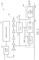
- the modulation circuit 260 may modulate the target signal CK1 by adjusting a pulse width of the target signal CK1.
- the modulation circuit 260 may narrow down the pulse width of the target signal CK1 to generate the modulated target signal CK2 having a pulse width narrower than that of the target signal CK1. Since the pulse width of the modulated target signal CK2 is narrower than that of the target signal CK1, the replica circuit 270 actually operates in a tighter condition than the functional circuit 210.
- the tighter condition may be utilized to detect whether an error caused by duty cycle degradation is about to or possibly to occur in the functional circuit 210.
- the error detection result may be an error detection signal having a default signal level that is utilized to indicate an errorless condition and a predetermined signal level that is utilized to indicate a detected error.
- a high voltage level may be set or an error flag may be asserted in the error detection signal when an error has been detected by the error detection circuit 280.
- the label Err_Flag is given to the error detection result or the error detection signal outputted by the error detection circuit 280.
- the error detection circuit 280 may be arranged to compare a difference between the first output signal Q1 and the second output signal Q2 to generate the error detection signal Err Flag.
- the error detection circuit 280 may be designed to detect whether the second output signal Q2 has the same value as the first output signal Q1 and accordingly generate the error detection signal Err Flag.
- the error detection circuit 280 may be implemented as or comprise an exclusive OR (XOR) gate.
- the error detection signal Err_Flag is further provided to the control circuit 230.
- the control circuit 230 is arranged to control the duty margin (or, in some embodiments, the duty cycle) of the target signal based on the error detection signal Err Flag. For example, when the control circuit 230 detects that an error flag is asserted in the error detection signal Err_Flag (or, when the error detection signal Err Flag is set to the predetermined signal level), the control circuit 230 adjusts the duty margin of the target signal. Preferably, the control circuit 230 may extend or increase the duty margin or the duty cycle of the target signal, since the error detection result indicates that the duty margin or duty cycle of the modulated target signal CK2 is insufficient.
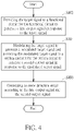
- Step S406 Comparing the first output signal and the second output signal and accordingly generating an error detection result according to the first output signal and the second output signal.
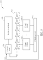
- the circuit 500 is designed to monitor and control the duty margin of a target signal, where the duty margin monitoring circuit in the circuit subunits is arranged to monitor the duty margin of the target signal by monitoring the signal output by the functional circuit in the circuit subunits and the control circuit 530 is arranged to control the duty margin (or, in some embodiments, the duty cycle) of the target signal and provide the target signal to a delay chain 540 and a subsequent digital circuit block 550.
- the target signal may be a pulse signal comprising only one or at least one pulse, or may be a clock signal comprising a plurality of consecutive pulses.
- the functional circuits in the circuit subunits 520-1-520-N may receive the target signal generated by the control circuit 530 with the same or different amounts of delay from the delay chain 540.
- the duty margin monitoring circuit in each circuit subunit may monitor the duty margin of the target signal from different delay points.
- the duty margin monitoring circuit in each circuit subunit may further comprise an error detection circuit, such as the error detection circuit 280 shown in FIG. 2 , coupled to the functional circuit and the replica circuit to receive the first output signal and the second output signal and arranged to generate the error detection result according to the first output signal and the second output signal.
- the error detection circuit may compare a difference between the first output signal and the second output signal to generate the error detection result.
- the error detection result generated by each circuit subunit may be an error detection signal having a default signal level that is utilized to indicate an errorless condition and a predetermined signal level that is utilized to indicate a detected error as discussed above. For example, a high voltage level may be set or an error flag may be asserted in the error detection signal when an error has been detected.
- the control circuit 530 is coupled to the collection circuit 510 and arranged to adjust the duty margin (or, in some embodiments, the duty cycle) of the target signal according to the control signal Ctrl. For example, when the control circuit 530 detects that the control signal Ctrl is set to the high voltage level (or, an error flag is asserted in the control signal Ctrl), the control circuit 530 adjusts the duty margin of the target signal. Preferably, the control circuit 530 may extend or increase the duty margin or the duty cycle of the target signal, since the high voltage level or the error flag asserted in the control signal Ctrl indicates that the duty margin or duty cycle of the modulated target signal is insufficient.
- the error detection circuit 680 is coupled to the functional circuit 610 and the replica circuit 670 to receive the first output signal and the second output signal and arranged to generate an error detection result according to the first output signal and the second output signal. It is to be noted that the circuit 600 has a similar structure and functions in a similar way as the circuit 200 shown in FIG. 2 . Therefore, the detailed descriptions of the circuit 600 may refer to descriptions of FIG. 2 , where like numbers refer to like elements.
- FIG. 7 shows an exemplary circuit diagram of a modulation circuit according to an embodiment of the invention.
- the modulation circuit 760 may comprise an inverter, a delay circuit and a logical gate, such as an AND gate.
- the modulation circuit 760 may perform the logical operation, such as the logical AND operation, on the target signal CK1 and an inverted and delayed version of the target signal CK1 to generate the modulated target signal CK2, where the amount of delay may be determined based on reserved margin to be monitored.
- FIG. 7 shows only an exemplary circuit of a modulation circuit, and the invention should not be limited thereto.
- the pulse width of the modulated target signal CK2 generated by the modulation circuit will be narrower than that of the target signal CK1, so as to create a tighter condition for the replica circuit as a comparison.
- the duty margin or duty cycle will be adjusted by the control circuit in advance, so as to avoid function failure of the functional circuit caused by duty cycle degradation and/or avoid the error to actually occur.
Landscapes
- Physics & Mathematics (AREA)
- Engineering & Computer Science (AREA)
- Theoretical Computer Science (AREA)
- Nonlinear Science (AREA)
- Probability & Statistics with Applications (AREA)
- General Engineering & Computer Science (AREA)
- General Physics & Mathematics (AREA)
- Manipulation Of Pulses (AREA)
- Pulse Circuits (AREA)
Applications Claiming Priority (2)
| Application Number | Priority Date | Filing Date | Title |
|---|---|---|---|
| US202063117505P | 2020-11-24 | 2020-11-24 | |
| US17/504,485 US11611334B2 (en) | 2020-11-24 | 2021-10-18 | Method and circuit for monitoring and controlling duty margin of a signal |
Publications (3)
| Publication Number | Publication Date |
|---|---|
| EP4002691A2 true EP4002691A2 (de) | 2022-05-25 |
| EP4002691A3 EP4002691A3 (de) | 2022-08-10 |
| EP4002691B1 EP4002691B1 (de) | 2026-03-04 |
Family
ID=78413633
Family Applications (1)
| Application Number | Title | Priority Date | Filing Date |
|---|---|---|---|
| EP21204691.6A Active EP4002691B1 (de) | 2020-11-24 | 2021-10-26 | Verfahren und schaltung zur überwachung und steuerung der einschaltdauer eines signals |
Country Status (4)
| Country | Link |
|---|---|
| US (1) | US11611334B2 (de) |
| EP (1) | EP4002691B1 (de) |
| CN (1) | CN114553197A (de) |
| TW (1) | TWI796843B (de) |
Families Citing this family (1)
| Publication number | Priority date | Publication date | Assignee | Title |
|---|---|---|---|---|
| JP7618522B2 (ja) * | 2021-09-10 | 2025-01-21 | キオクシア株式会社 | 半導体集積回路、及び、半導体記憶装置、並びに、メモリシステム |
Family Cites Families (14)
| Publication number | Priority date | Publication date | Assignee | Title |
|---|---|---|---|---|
| US7298807B2 (en) | 2003-02-11 | 2007-11-20 | Rambus Inc. | Circuit, apparatus and method for adjusting a duty-cycle of a clock signal in response to incoming serial data |
| KR100534211B1 (ko) * | 2004-06-23 | 2005-12-08 | 삼성전자주식회사 | 반도체 장치에 있어서의 듀티 사이클 보정회로 |
| JP2007121114A (ja) * | 2005-10-28 | 2007-05-17 | Elpida Memory Inc | デューティ検知回路、これらを備えたdll回路及び半導体装置 |
| WO2008032701A1 (fr) * | 2006-09-13 | 2008-03-20 | Nec Corporation | Circuit d'ajustement d'horloge et dispositif de circuit intégré à semi-conducteurs |
| KR100863001B1 (ko) * | 2007-02-09 | 2008-10-13 | 주식회사 하이닉스반도체 | 듀티 싸이클 보정 기능을 갖는 지연 고정 루프 회로 및 그제어방법 |
| KR101030275B1 (ko) * | 2009-10-30 | 2011-04-20 | 주식회사 하이닉스반도체 | 듀티 보정 회로 및 이를 포함하는 클럭 보정 회로 |
| KR101103070B1 (ko) | 2010-04-30 | 2012-01-06 | 주식회사 하이닉스반도체 | 클럭 신호 듀티 보정 회로 |
| US8542045B2 (en) * | 2010-06-07 | 2013-09-24 | Samsung Electronics Co., Ltd. | Duty correcting circuit, delay-locked loop circuit and method of correcting duty |
| US8803605B2 (en) * | 2011-02-01 | 2014-08-12 | Mediatek Singapore Pte. Ltd. | Integrated circuit, wireless communication unit and method for providing a power supply |
| WO2012145117A2 (en) | 2011-04-22 | 2012-10-26 | Rambus Inc. | Memory components and controllers that calibrate multiphase synchronous timing references |
| EP3072239A4 (de) | 2013-11-19 | 2017-06-21 | Intel Corporation | Uhrenkalibrierung mit asynchroner digitaler abtastung |
| US9535119B2 (en) * | 2014-06-30 | 2017-01-03 | Intel Corporation | Duty cycle based timing margining for I/O AC timing |
| US10516391B2 (en) * | 2017-12-12 | 2019-12-24 | Micron Technology, Inc. | Apparatuses and methods for data transmission offset values in burst transmissions |
| US11832249B2 (en) * | 2019-05-13 | 2023-11-28 | Qualcomm Incorporated | Dynamic duty cycle |
-
2021
- 2021-10-18 US US17/504,485 patent/US11611334B2/en active Active
- 2021-10-26 EP EP21204691.6A patent/EP4002691B1/de active Active
- 2021-11-22 TW TW110143333A patent/TWI796843B/zh active
- 2021-11-23 CN CN202111393689.5A patent/CN114553197A/zh active Pending
Also Published As
| Publication number | Publication date |
|---|---|
| US11611334B2 (en) | 2023-03-21 |
| CN114553197A (zh) | 2022-05-27 |
| US20220166412A1 (en) | 2022-05-26 |
| EP4002691B1 (de) | 2026-03-04 |
| TWI796843B (zh) | 2023-03-21 |
| EP4002691A3 (de) | 2022-08-10 |
| TW202222038A (zh) | 2022-06-01 |
Similar Documents
| Publication | Publication Date | Title |
|---|---|---|
| US11100224B2 (en) | Interference detection device and detection sensitivity adjusting method thereof | |
| JP2608609B2 (ja) | フェーズ・ロック・ループ回路 | |
| US5798720A (en) | Parallel to serial data converter | |
| US8502577B2 (en) | Phase correction circuit, data alignment circuit and method of aligning data using the same | |
| US9124257B2 (en) | Digital clock placement engine apparatus and method with duty cycle correction and quadrature placement | |
| US9479148B2 (en) | Serial data signal edge detection | |
| US10038432B2 (en) | Duty correction circuit | |
| US20160112184A1 (en) | Clock and data recovery circuit and method | |
| US20220006460A1 (en) | Timing Margin Detecting Circuit, Timing Margin Detecting Method and Clock and Data Recovery System | |
| US6622256B1 (en) | System for protecting strobe glitches by separating a strobe signal into pointer path and timing path, filtering glitches from signals on pointer path thereof | |
| US11611334B2 (en) | Method and circuit for monitoring and controlling duty margin of a signal | |
| CN115903998A (zh) | 校准方法、电路、存储介质、时钟恢复电路及电子装置 | |
| EP0499397B1 (de) | Digitales Kommunikationssystem | |
| US7003043B2 (en) | Replica driver mismatch correction using a variable offset comparator | |
| EP4195510A1 (de) | Verzögerungsregelschleife | |
| US6239629B1 (en) | Signal comparison system and method for detecting and correcting timing errors | |
| US20090027093A1 (en) | Sampling circuit and method | |
| US11398824B2 (en) | Delay locked loop circuit | |
| US6356610B1 (en) | System to avoid unstable data transfer between digital systems | |
| US20200162064A1 (en) | Debounce circuit using d flip-flops | |
| US20070216456A1 (en) | Delay locked loop and method of locking a clock signal | |
| US6420915B2 (en) | Signal comparison system and method for detecting and correcting timing errors | |
| CN100527626C (zh) | 可防止假锁定发生的延迟锁定回路及相关方法 | |
| US6665218B2 (en) | Self calibrating register for source synchronous clocking systems | |
| US20200412349A1 (en) | Method and circuit used to obtain time limits for obtaining clock edge adjustment value to adjust clock edge of clock signal accordingly |
Legal Events
| Date | Code | Title | Description |
|---|---|---|---|
| PUAI | Public reference made under article 153(3) epc to a published international application that has entered the european phase |
Free format text: ORIGINAL CODE: 0009012 |
|
| STAA | Information on the status of an ep patent application or granted ep patent |
Free format text: STATUS: THE APPLICATION HAS BEEN PUBLISHED |
|
| AK | Designated contracting states |
Kind code of ref document: A2 Designated state(s): AL AT BE BG CH CY CZ DE DK EE ES FI FR GB GR HR HU IE IS IT LI LT LU LV MC MK MT NL NO PL PT RO RS SE SI SK SM TR |
|
| PUAL | Search report despatched |
Free format text: ORIGINAL CODE: 0009013 |
|
| AK | Designated contracting states |
Kind code of ref document: A3 Designated state(s): AL AT BE BG CH CY CZ DE DK EE ES FI FR GB GR HR HU IE IS IT LI LT LU LV MC MK MT NL NO PL PT RO RS SE SI SK SM TR |
|
| RIC1 | Information provided on ipc code assigned before grant |
Ipc: H03K 5/156 20060101AFI20220701BHEP |
|
| STAA | Information on the status of an ep patent application or granted ep patent |
Free format text: STATUS: REQUEST FOR EXAMINATION WAS MADE |
|
| 17P | Request for examination filed |
Effective date: 20230207 |
|
| RBV | Designated contracting states (corrected) |
Designated state(s): AL AT BE BG CH CY CZ DE DK EE ES FI FR GB GR HR HU IE IS IT LI LT LU LV MC MK MT NL NO PL PT RO RS SE SI SK SM TR |
|
| P01 | Opt-out of the competence of the unified patent court (upc) registered |
Effective date: 20230607 |
|
| GRAP | Despatch of communication of intention to grant a patent |
Free format text: ORIGINAL CODE: EPIDOSNIGR1 |
|
| STAA | Information on the status of an ep patent application or granted ep patent |
Free format text: STATUS: GRANT OF PATENT IS INTENDED |
|
| INTG | Intention to grant announced |
Effective date: 20251006 |
|
| GRAS | Grant fee paid |
Free format text: ORIGINAL CODE: EPIDOSNIGR3 |
|
| GRAA | (expected) grant |
Free format text: ORIGINAL CODE: 0009210 |
|
| STAA | Information on the status of an ep patent application or granted ep patent |
Free format text: STATUS: THE PATENT HAS BEEN GRANTED |
|
| AK | Designated contracting states |
Kind code of ref document: B1 Designated state(s): AL AT BE BG CH CY CZ DE DK EE ES FI FR GB GR HR HU IE IS IT LI LT LU LV MC MK MT NL NO PL PT RO RS SE SI SK SM TR |
|
| REG | Reference to a national code |
Ref country code: CH Ref legal event code: F10 Free format text: ST27 STATUS EVENT CODE: U-0-0-F10-F00 (AS PROVIDED BY THE NATIONAL OFFICE) Effective date: 20260304 Ref country code: GB Ref legal event code: FG4D |
|
| REG | Reference to a national code |
Ref country code: DE Ref legal event code: R096 Ref document number: 602021049116 Country of ref document: DE |
|
| REG | Reference to a national code |
Ref country code: IE Ref legal event code: FG4D |
|
| PG25 | Lapsed in a contracting state [announced via postgrant information from national office to epo] |
Ref country code: RS Free format text: LAPSE BECAUSE OF FAILURE TO SUBMIT A TRANSLATION OF THE DESCRIPTION OR TO PAY THE FEE WITHIN THE PRESCRIBED TIME-LIMIT Effective date: 20260604 |
|
| PG25 | Lapsed in a contracting state [announced via postgrant information from national office to epo] |
Ref country code: ES Free format text: LAPSE BECAUSE OF FAILURE TO SUBMIT A TRANSLATION OF THE DESCRIPTION OR TO PAY THE FEE WITHIN THE PRESCRIBED TIME-LIMIT Effective date: 20260304 |
|
| REG | Reference to a national code |
Ref country code: NL Ref legal event code: MP Effective date: 20260304 |
|
| PG25 | Lapsed in a contracting state [announced via postgrant information from national office to epo] |
Ref country code: PL Free format text: LAPSE BECAUSE OF FAILURE TO SUBMIT A TRANSLATION OF THE DESCRIPTION OR TO PAY THE FEE WITHIN THE PRESCRIBED TIME-LIMIT Effective date: 20260304 |
|
| PG25 | Lapsed in a contracting state [announced via postgrant information from national office to epo] |
Ref country code: GR Free format text: LAPSE BECAUSE OF FAILURE TO SUBMIT A TRANSLATION OF THE DESCRIPTION OR TO PAY THE FEE WITHIN THE PRESCRIBED TIME-LIMIT Effective date: 20260605 |
|
| REG | Reference to a national code |
Ref country code: LT Ref legal event code: MG9D |
|
| PG25 | Lapsed in a contracting state [announced via postgrant information from national office to epo] |
Ref country code: LT Free format text: LAPSE BECAUSE OF FAILURE TO SUBMIT A TRANSLATION OF THE DESCRIPTION OR TO PAY THE FEE WITHIN THE PRESCRIBED TIME-LIMIT Effective date: 20260304 |
|
| PG25 | Lapsed in a contracting state [announced via postgrant information from national office to epo] |
Ref country code: NO Free format text: LAPSE BECAUSE OF FAILURE TO SUBMIT A TRANSLATION OF THE DESCRIPTION OR TO PAY THE FEE WITHIN THE PRESCRIBED TIME-LIMIT Effective date: 20260604 |
|
| PG25 | Lapsed in a contracting state [announced via postgrant information from national office to epo] |
Ref country code: SE Free format text: LAPSE BECAUSE OF FAILURE TO SUBMIT A TRANSLATION OF THE DESCRIPTION OR TO PAY THE FEE WITHIN THE PRESCRIBED TIME-LIMIT Effective date: 20260304 Ref country code: FI Free format text: LAPSE BECAUSE OF FAILURE TO SUBMIT A TRANSLATION OF THE DESCRIPTION OR TO PAY THE FEE WITHIN THE PRESCRIBED TIME-LIMIT Effective date: 20260304 |
|
| PG25 | Lapsed in a contracting state [announced via postgrant information from national office to epo] |
Ref country code: HR Free format text: LAPSE BECAUSE OF FAILURE TO SUBMIT A TRANSLATION OF THE DESCRIPTION OR TO PAY THE FEE WITHIN THE PRESCRIBED TIME-LIMIT Effective date: 20260304 |
|
| PG25 | Lapsed in a contracting state [announced via postgrant information from national office to epo] |
Ref country code: LV Free format text: LAPSE BECAUSE OF FAILURE TO SUBMIT A TRANSLATION OF THE DESCRIPTION OR TO PAY THE FEE WITHIN THE PRESCRIBED TIME-LIMIT Effective date: 20260304 |
|
| PG25 | Lapsed in a contracting state [announced via postgrant information from national office to epo] |
Ref country code: BG Free format text: LAPSE BECAUSE OF FAILURE TO SUBMIT A TRANSLATION OF THE DESCRIPTION OR TO PAY THE FEE WITHIN THE PRESCRIBED TIME-LIMIT Effective date: 20260304 |