EP3993265A1 - Procédé de commutation des transistors de puissance - Google Patents
Procédé de commutation des transistors de puissance Download PDFInfo
- Publication number
- EP3993265A1 EP3993265A1 EP20465573.2A EP20465573A EP3993265A1 EP 3993265 A1 EP3993265 A1 EP 3993265A1 EP 20465573 A EP20465573 A EP 20465573A EP 3993265 A1 EP3993265 A1 EP 3993265A1
- Authority
- EP
- European Patent Office
- Prior art keywords
- switching
- current
- power transistor
- miller plateau
- bridge
- Prior art date
- Legal status (The legal status is an assumption and is not a legal conclusion. Google has not performed a legal analysis and makes no representation as to the accuracy of the status listed.)
- Pending
Links
Images


Classifications
-
- H—ELECTRICITY
- H03—ELECTRONIC CIRCUITRY
- H03K—PULSE TECHNIQUE
- H03K17/00—Electronic switching or gating, i.e. not by contact-making and –breaking
- H03K17/16—Modifications for eliminating interference voltages or currents
- H03K17/161—Modifications for eliminating interference voltages or currents in field-effect transistor switches
- H03K17/162—Modifications for eliminating interference voltages or currents in field-effect transistor switches without feedback from the output circuit to the control circuit
- H03K17/163—Soft switching
-
- H—ELECTRICITY
- H03—ELECTRONIC CIRCUITRY
- H03K—PULSE TECHNIQUE
- H03K17/00—Electronic switching or gating, i.e. not by contact-making and –breaking
- H03K17/16—Modifications for eliminating interference voltages or currents
- H03K17/161—Modifications for eliminating interference voltages or currents in field-effect transistor switches
- H03K17/165—Modifications for eliminating interference voltages or currents in field-effect transistor switches by feedback from the output circuit to the control circuit
- H03K17/166—Soft switching
Definitions
- a method for switching on or off an electronic component, controlled by means of a pulse width modulation signal, which is designed to output an output signal that can be controlled by means of a control signal is initiated within a pulse width modulation clock period at a level change time by a change in the pulse width modulation signal. At least a first control value and a second control value of the control signal are specified and the control signal is set to the first control value within each pulse width modulation clock period between the time of the level change and a first switching time, to the second control value between the first switching time and a second switching time and from the second switching time to set to a third control value in order to reach a final gate voltage value at the gate of the electronic component.
- Each switchover time of a pulse width modulation clock period is determined as a function of an amplitude value determined during a preceding pulse width modulation clock period in such a way that oscillation amplitudes of the oscillation of the output signal are limited.
- the invention is based on the object of specifying an improved method for switching power transistors.
- the power transistors each having a gate
- the gate is driven sequentially in a switch-on sequence and/or a switch-off sequence with at least three control values, between which there is a switchover at specific times.
- the points in time are determined or modified by means of a controller which is controlled by a Miller plateau detector for detecting a Miller plateau in a gate-source voltage of the respective power transistor.
- the at least three control values can differ from one another and/or be different from zero, but can also partially match.
- the first control value and the third control value can be the same.
- the Miller plateau detector is supplied with a phase voltage of a half-bridge that is part of the power transistor circuit, or any voltage or current of this half-bridge, for example a drain-source voltage or a gate-source voltage, for detecting the Miller plateau.
- the Miller plateau detector can also be based on the detection of voltage transients at a source connection of a power transistor in the lower bridge branch of this half bridge or on the detection of overshoots.
- the Miller plateau detector is used to detect when the Miller plateau begins or when the Miller plateau begins and ends. In one embodiment, the Miller plateau is detected in each duty cycle in which the respective power transistor is not freewheeling, and this information is used to adjust the timing for the next duty cycle in which the respective power transistor is not freewheeling.
- the power transistor in particular MOSFET, is referred to as freewheeling in the present application if the power transistor (if the power transistor is switched on) or a body diode (if the power transistor is not switched on) of the power transistor carries a freewheeling current of an inductive load.
- the Miller plateau is detected using the phase voltage by means of a comparator contained in the Miller plateau detector.
- the change from a first control value, for example at a gate of the power transistor, in particular MOSFETs, to a second control value takes place by a time difference before the start of the Miller plateau and/or the change from the second control value to a third control value takes place when Turning on takes place by a time difference after the start of the Miller plateau and/or when turning off, the change from the first control value to the second control value takes place by a time difference after the Miller plateau has been reached.
- the change from the first control value to the second control value can take place by a time difference after the Miller plateau has been reached.
- the second control value is adjusted during turn-on and turn-off of the power transistor depending on a level of a load current.
- At least three control values are used to drive non-freewheeling power transistors in the power transistor circuit, while freewheeling power transistors are driven with a constant control value.
- the phase voltage is measured during a dead time during which both power transistors of the half-bridge are switched off, and when the phase voltage is low, the power transistor is in a lower Branch of the half-bridge is recognized as free-running in the next working cycle.
- a power transistor that was driven to turn on with at least three different control values is basically also driven to turn off in the same duty cycle with at least three different control values, and a power transistor that is turned on with a constant control value was controlled, is basically also for Turn-off driven in the same duty cycle with constant control value, except when a long pulse is detected causing a change in polarity of the phase current of the respective half-bridge.
- a counter is started, the count of which is incremented by one each time a new duty cycle is applied to one of the other half-bridges, and when the counter has a has reached a certain value, the switching off of the power transistor is carried out using at least three different control values.
- the points in time and/or at least one target value of at least one of the time differences are varied as a function of the load current.
- the second control value when using at least three control values, is adjusted during switching on and off of the power transistor according to the level of the load current.
- the control value that is applied at the end of the Miller Plateau can be adjusted.
- control values are adjusted using a source controlled by the controller operating in a current source mode, the source being switched from the current source mode to a voltage source mode at the end of the turn-on sequence and/or the turn-off sequence.
- the operating strategy for MOSFETs proposed according to the present invention enables the MOSFETs to be switched and power losses to be reduced without causing increased electromagnetic emissions. This is achieved with special features implemented in an integrated circuit, such as an ASIC or ASSP, and without additional external components, thus reducing costs and space requirements and by Additional switching losses caused by external components are avoided, as these delay the entire switching. External components must be dimensioned for the worst case (worst case) and increase the switching times.
- the present invention does not require an overshoot detector with its attendant layout constraints and high resolution timers.
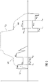
- figure 1 is a schematic circuit diagram of a power transistor circuit, in particular a bridge circuit 1, made up of power transistors for operating a load L, for example MOSFETs HS1, HS2, LS1, LS2 or IGBT, referred to below as MOSFETs HS1, HS2, LS1, LS2.
- the bridge circuit 1 is connected to a voltage source V .
- Each of the MOSFETs HS1, HS2, LS1, LS2 has a gate G, drain D and source S, the gate G being controllable by means of a gate driver circuit 2 which applies a pulse width modulated signal PWM to the gate G.
- the gate driver circuit 2 for the MOSFET LS1 is shown in detail.
- the other gate drive circuits 2 can be formed in the same way.
- one and the same gate driver circuit 2 can take over the gates G of all MOSFETs HS1, HS2, LS1, LS2 of the bridge circuit 1.
- the MOSFETs HS1, HS2, LS1, LS2 are arranged in two half-bridges HB1, HB2, with the MOSFETs HS1, LS1 being assigned to the half-bridge HB1 and the MOSFETs HS2, LS2 to the half-bridge HB2.
- a further detector 2.5 can be provided in the gate driver circuit 2, which is configured to detect whether the switching cycle has ended, ie whether the MOSFET HS1, HS2, LS1, LS2 is completely switched off.
- a pulse width modulation controlled bridge circuit 1 made of MOSFETs HS1, HS2, LS1, LS2, for example an H-bridge, a half-bridge HB1, HB2 or other configurations can be used in various applications, for example in motor driver circuits or inverters.
- the MOSFETs HS1, HS2, LS1, LS2 are controlled by means of a pulse width modulated signal in order to apply a desired voltage and/or current profile to the load L.
- the invention enables the emissions to be limited and the switching time to be minimized by appropriately shaping a gate current I g of the MOSFET HS1, HS2, LS1, LS2 during an on/off sequence of the MOSFET HS1, HS2, LS1, LS2.
- figure 8 shows a schematic diagram with a switching sequence of a MOSFET HS, LS.
- the gate current I g starts with a high current value Ig1 ON , at a time t1 ON it is switched to a lower current value Ig2 ON and at a time t2 ON it is switched again to a high current value Ig3 ON which is not related to the current value Ig1 ON must be identical, but can be.
- the current values Ig1 ON , Ig2 ON , Ig3 ON are predefined values.
- the times t1 ON and t2 ON are determined by the gate driver circuit 2 using a regulator 2.1, which is controlled by a Miller plateau detector 2.2 for detecting a Miller plateau MP.
- the controller 2.1 controls a source 2.4 that defines the gate current I g .
- the gate current I g starts with a high current value Ig1 OFF , at a time t1 OFF it is switched to a lower current value Ig2 OFF and at a time t2 OFF it is switched again to a high current value Ig3 OFF which is not related to the current value Ig1 OFF must be identical.
- the current values Ig1 OFF , Ig2 OFF , Ig3 OFF are predefined values.
- the times t1 OFF and t2 OFF are determined by the gate driver circuit 2 using a controller 2.1, which is controlled by a Miller plateau detector 2.2 for detecting a Miller plateau MP. The regulation is carried out over several working cycles of the pulse width modulation.
- the gate driver circuit 2 has a measuring connection 2.3, by means of which a phase voltage V PHASE of the respective half-bridge HB1, HB2 can be measured and fed to the Miller plateau detector 2.2.
- a phase voltage V PHASE of the respective half-bridge HB1, HB2 can be measured and fed to the Miller plateau detector 2.2.
- any current or any voltage of the half-bridge HB1, HB2 can be measured by the measuring connection 2.3.
- Another example is a peak detector that monitors voltage transients at the source of the MOSFET LS in the lower bridge arm.
- Gate voltage change rates can also be used as control values instead of the current values.
- the method also allows the current value Ig2 to be adjusted based on the load current and can therefore better adapt the gate current profile to the switching process.
- MOSFETs HS, LS are normally uncritical with regard to electromagnetic compatibility.
- the invention describes a way of detecting MOSFETs HS, LS that are critical with regard to electromagnetic compatibility, and of applying the method described for shaping the gate current I g only to these MOSFETs HS, LS.
- free-running MOSFETs HS, LS can be operated with a constant gate current I g .
- the control circuit is based on the detection of the Miller plateau MP.
- the parameter with the highest dynamics affecting the Miller plateau MP is the load current I LOAD , that is, in motor driver circuits, the phase current I PHASE . It can happen that a controller 2.1 is too slow to follow the fluctuations in the load current I LOAD .
- controller 2.1 is designed as an I controller.
- figure 2 shows a schematic circuit diagram of a simplified half-bridge HB1.
- Half bridges HB1, HB2 for operating an inductive load L for example DC/DC converters, H-bridge motor driver circuits or B6 motor driver circuits, as figure 2 shown, simplified.
- the load current I LOAD always has the same polarity.
- the polarity of the load current I LOAD can change over time.
- the switching of the MOSFET HS in the upper bridge arm causes a rapid change in the supply current I S and in the phase voltage V PHASE and triggers ringing.
- the MOSFET LS in the lower bridge arm is in the freewheeling path and the switching of the MOSFET LS causes no ringing, no change in the supply current I S and only a small change in the phase voltage V PHASE .
- the switching of the MOSFET LS in the lower leg of the bridge causes a rapid change in the supply current and in the phase voltage V PHASE and triggers ringing.
- the MOSFET HS in the upper bridge leg is free running and the switching of the MOSFET HS causes no ringing, no change in the supply current and only a small change in the phase voltage V PHASE .
- Ringing and rapid changes in supply current and phase voltage VPHASE typically cause galvanically conducted or radiated emissions to exceed electromagnetic compatibility specifications. Overshoot and rapid changes in the supply current I S and in the phase voltage V PHASE can be reduced by driving the causing MOSFET HS, LS, i.e. the MOSFET HS with a positive load current I LOAD and the MOSFET LS with a negative load current I LOAD , accordingly .
- a dead time t d is always provided, during which both MOSFETs HS, LS of the half-bridge HB1 are switched off.
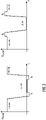
- the load current I LOAD flows in the body diode of the MOSFET HS, LS. If the load current I LOAD is positive, it flows in the body diode of the MOSFET LS. If the load current I LOAD is negative, it flows in the body diode of the MOSFET HS. Therefore, during the dead time t d , the phase voltage V PHASE is low when the phase current I PHASE is positive and the phase voltage V PHASE is high when the phase current I PHASE is negative, as in FIG figure 3 shown.
- figure 3 shows schematic diagrams of the phase voltage V PHASE over time t when switching the MOSFETs HS, LS, with a switching state HS ON the switched-on MOSFET HS symbolizes in the upper branch of the bridge and LS ON symbolizes the switched-on MOSFET LS in the lower branch of the bridge.
- the device in which the present invention is implemented i.e. the gate drive circuit 2 can detect whether both MOSFETs HS, LS are off and measure the phase voltage V PHASE during the dead time t d .
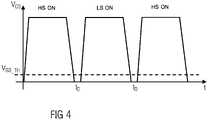
- One way to detect that both MOSFETS HS, LS are off is to check when the two gate-source voltages V GS of both MOSFETs HS, LS are below a threshold value V GS_TH at the same time as in figure 4 is shown.
- figure 4 shows a schematic diagram of the gate-source voltage V GS of a MOSFET HS, LS over time t when switching the MOSFET HS, LS.
- phase voltage V PHASE The measurement of the phase voltage V PHASE is then used to detect whether the next MOSFET to be turned on is free running or not as in in figure 10 illustrated algorithm is shown. If the phase voltage V PHASE is low, then the MOSFET HS in the upper arm of the Next, half bridges HB1 to HB3 are operated with at least three different current values Ig1, Ig2, Ig3. Otherwise, the MOSFET LS in the lower branch of the half-bridge HB1 to HB3 is next operated with at least three different current values Ig1, Ig2, Ig3.
- the magnitude of the phase voltage V PHASE can be determined using a hysteresis comparator.
- the phase voltage V PHASE is considered low if it is less than 25% of a specified value and high if it is greater than 75% of the specified value.
- Each half-bridge HB1 to HB3 has its own phase voltage V PHASE and the state of this phase voltage V PHASE during the dead time t D determines how the MOSFETs HS, LS of this half-bridge HB1 to HB3 are controlled.
- One or more half-bridges HB1 to HB3 can be provided.
- Three or more current values Ig1, Ig2, Ig3 for controlling the gate G can be provided.
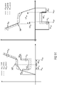
- figure 10 shows a schematic view of an algorithm for determining which MOSFET HS, LS of a half-bridge HB1, HB2 is free-running.
- next MOSFET HS, LS to be driven is free-running, it is driven with a constant gate current I g . Otherwise it is controlled during switching using at least three different current values Ig1, Ig2, Ig3, as in WO2014/173969 A1 described and in figure 5 for the free-wheeling MOSFET LS and figure 6 for the free-wheeling MOSFET HS.
- figure 5 shows a schematic diagram of a switching sequence of the half-bridge HB1 with a free-running MOSFET LS, with a Gate-source voltage V GS_LS of the MOSFET LS, a Gate-source voltage V GS_HS of the MOSFET HS, a gate current I g_LS of the MOSFET LS, a gate current I g_HS of the MOSFET HS and the Phase voltage V PHASE are shown.
- figure 6 shows a schematic diagram of a switching sequence of the half-bridge HB1 with free-running MOSFET HS, wherein a gate-source voltage V GS_LS of the MOSFET LS, a gate-source voltage V GS_HS of the MOSFET HS, a gate current I g_LS of the MOSFET LS, a gate current I g_HS of the MOSFET HS and the phase voltage V PHASE are shown .
- the gates G are driven in accordance with the in WO 2014/173969 A1 described control device and the method described for it, in particular according to the figures 1 and 3 to 18 and the description on pages 8 to 26.
- the WO 2014/173969 A1 is hereby fully incorporated by reference into the present patent application.
- Switching off is performed in the same way as switching on: if a gate current I g with at least three different current values Ig1, Ig2, Ig3 was used for switching on, then it is also used for switching off. If a constant current was used at turn-on, then it will also be used at turn-off, except when long pulses are detected that cause a change in polarity of the phase current I PHASE . In applications where a brushless DC motor is used, long pulses could be applied to either the MOSFET HS or the MOSFET LS. These pulses cause the polarity inversion of the phase current I PHASE as in figure 7 is shown.
- figure 7 shows a schematic circuit diagram of a bridge circuit 1 for operating a three-phase electric motor M, three half-bridges HB1, HB2, HB3 being provided for one phase P1, P2, P3 each. Furthermore, a schematic diagram is shown in which the phase current I PHASE1 of the first half-bridge HB1 and the switching state LS1_PULSE of the MOSFET LS1 of the first half-bridge HB1, the switching state HB2_PULSE of the second half-bridge HB2 and the switching state HB3_PULSE of the third half-bridge HB3 are plotted against time t.
- the switching states HB2_PULSE and HB3_PULSE correspond to the pulse width modulated signals for controlling the half bridges HB2, HB3.
- the MOSFET LS1, LS2, LS3 in the lower bridge branch of the respective half-bridge HB1, HB2, HB3 can be switched on when the respective pulse width modulated signal has a low level and the MOSFET HS1, HS2, HS3 in the upper bridge branch of the respective half-bridge HB1, HB2 , HB3 can be switched on when the respective pulse width modulated signal has a high level.
- the pulse width modulated signals are only shown with different amplitudes for better visibility.
- the switching state LS1_PULSE corresponds to an inverted switching state HB1_PULSE (not shown).
- the gate driver circuit 2 in which the invention is implemented is able to detect long pulses of both MOSFETs HS and LS of each half-bridge HB1, HB2, HB3 by counting the pulses on the other half-bridges HB1, HB2, HB3.
- a counter is therefore started when the MOSFET LS1 is switched on. The count is incremented by one each time a new pulse width modulation duty cycle is applied to any of the other half bridges HB2, HB3.
- the MOSFET LS1 is switched off using at least three different current values Ig1, Ig2, Ig3.
- the present invention is therefore a further development of WO2014/173969 A1 described procedure.
- the overshoot measurement can be replaced by any other method for detecting the Miller plateau MP.
- the times t1 ON , t2 ON for switching on and the times t1 OFF and t2 OFF for switching off can be calculated and adjusted based on them as in figure 9 shown.
- figure 9 shows a schematic diagram with a switching sequence of a MOSFET HS, LS. For example, when switching on, the change from the current value Ig1 ON to the current value Ig2 ON takes place by a time difference ⁇ t1 ON before the start of the Miller plateau MP.
- the change from the current value Ig2 ON to the current value Ig3 ON takes place when switching on by a time difference ⁇ t2 ON after the start of the Miller plateau MP.
- the change from the current value Ig1 OFF to the current value Ig2 OFF takes place by a time difference ⁇ t1 OFF after the Miller plateau MP has been reached.
- the change from the current value Ig2 OFF to the current value Ig3 OFF takes place with a delay of a time difference ⁇ t2 OFF when switching off.
- the time differences ⁇ t1 ON , ⁇ t2 ON , ⁇ t1 OFF and ⁇ t2 OFF can be positive or negative depending on the needs of the application.
- the Miller plateau MP is detected in each duty cycle of the pulse width modulation in which the MOSFET LS, HS is not free-running, and this information is used to determine the times t1 ON t2 ON for switching on and adjust the times t1 OFF and t2 OFF for switching off in order to get the time differences ⁇ t1 ON , ⁇ t2 ON , ⁇ t1 OFF and ⁇ t2 OFF in the next working cycle closer to a target value of the time difference ⁇ t1 ONSET , ⁇ t2 ONSET , ⁇ t1 OFFSET , ⁇ t2 OFFSET , as in figure 11 is shown.
- figure 11 is a schematic view of one State machine of the MOSFET HS or LS for adjusting the times t1 ON , t2 ON for switching on and the times t1 OFF and t2 OFF for switching off if the respective MOSFET HS, LS is operated with at least three current values Ig1, Ig2, Ig3.
- figure 11 1 represents a possible embodiment of the controller 2.1.
- a switch-on command is given for the MOSFET HS, LS, a timer is started and the MOSFET HS, LS is driven with the gate current I g .
- the Miller plateau detector 2.2 on Miller plateau MP is detected, the corresponding point in time t MON is stored.
- the time difference ⁇ t1 ON is then determined as the difference between the times t MON and t1 ON and the time difference ⁇ t2 ON is determined as the difference between the times t2 ON and t MON .
- the relevant times t1 ON , t2 ON , t1 OFF and T2 OFF are increased/decreased by an increment t1 ONINC , t2 ONINC , t1 OFFINC and t2 OFFINC which can be constant or proportional to the error signal (difference between the target value ⁇ t and the measured value ⁇ t).
- the regulation of the times t1 ON , t2 ON , t1 OFF and T2 OFF is based on the detection of the Miller plateau MP.
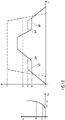
- the load current I LOAD is usually the parameter with the fastest dynamics that can affect the Miller plateau MP. If the load current I LOAD or the drain current Id is increased from a current value Id1 to a current value Id2, the voltage VM1, VM2 of the Miller plateau MP also increases as in FIG figure 12 shown (both the transfer properties as well as the curves in the time domain).
- the times t1 ON , t2 ON , t1 OFF and T2 OFF should be adjusted according to the voltage VM1, VM2 of the Miller plateau MP in order to maintain the desired time differences ⁇ t1 ON , ⁇ t2 ON , ⁇ t1 OFF and ⁇ t2 OFF . If, for example, the voltage VM1, VM2 of the Miller plateau MP increases, then the time t1 ON should also be increased in order to obtain the desired time difference ⁇ t1 ON .
- a default value t x_DEF is defined for each point in time t1 ON , t2 ON , t1 OFF and t2 OFF . The default value t x_DEF is used at the beginning to initialize the controller 2.1.
- a ratio (linear or non-linear as required) to the load current I LOAD as in figure 13 Only linear cases are shown.
- the regulator 2.1 can then carry out the regulation and find the optimum value.
- the constant factor K can be fixed for the respective application.
- a controller 2.1 according to the second embodiment is based on the first embodiment.
- the gate current Ig in the second section is reduced to the second current value Ig2 during commutation (switching) so that the overshoot remains within an acceptable range.
- the detection of the Miller plateau MP together with maintaining the target values of the time difference ⁇ t1 ONSET , ⁇ t2 ONSET , ⁇ t1 OFFSET and ⁇ t2 OFFSET ensures that the gate G of the MOSFET HS, LS during commutation (switching) with the selected second current value Ig2 of the gate current I g is controlled.
- a fixed current value Ig2 of the gate current I g is not optimal for the entire range of load currents I LOAD .
- the second current value Ig2 can be adjusted during turn-on and turn-off of the MOSFET HS, LS according to the level of the load current I LOAD (see Figure 14).
- figure 14 shows a schematic diagram of a turn-on sequence on the left and a schematic diagram of a turn-off sequence of a MOSFET HS, LS on the right.
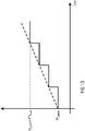
- the range of load currents I LOAD is divided into N sub-ranges as in figure 15 shown.
- figure 15 12 is a schematic diagram of the second current value Ig2 of the gate current I g versus the load current I LOAD .
- Each sub-range corresponds to a specific current value Ig2.
- the slope of this curve is determined according to electromagnetic compatibility and loss requirements.
- the current value Ig2 is adjusted to regulate the target values of the time difference ⁇ t1 ONSET , ⁇ t2 ONSET , ⁇ t1 OFFSET and ⁇ t2 OFFSET .
- the specified values of the time difference ⁇ tx are controlled in the same way as in figure 11 shown flowchart. For example, if ⁇ t1 ON is greater than ⁇ t1 ONSET , then Ig2 ON is increased by an increment of Ig2 ONINC . Conversely, if ⁇ t1 ON is less than ⁇ t1 ONSET , Ig2 ON is decreased by the increment Ig2 ONINC .
- the target values of the time difference ⁇ t1 ONSET , ⁇ t2 ONSET , ⁇ t1 OFFSET and ⁇ t2 OFFSET are functions of the division of the load current I LOAD .
- FIG. 16 is a schematic diagram of the desired value ⁇ tx ONSET versus load current I LOAD .
- FIG. 12 is a schematic diagram showing the overshoot behavior for different second current values Ig2(1) to Ig2(4) of the gate current I g .
- figure 18 12 is a schematic diagram showing the loss behavior for different second current values Ig2(1) to Ig2(4) of the gate current I g . Since the method provides ⁇ tx SET values for different load current ranges, the control algorithm chooses different current values Ig2 depending on the sub-range of the load current I LOAD . This allows more flexibility to optimize electromagnetic compatibility and switching losses. For example, if Ig2 varies from Ig2(4) to Ig2(1), then the areas above the dashed line are performance gains.
- the second current value Ig2(1) is lowest and the second current value Ig2(4) is highest.
- Ig2(4) is chosen as the second current value, the MOSFET will switch from off to on or from on to off faster because the gate charges faster. Therefore, the power loss during switching is lower, but the level of overshoot is higher.
- the default values for t1 on , t2 on , t1 off and t1 off are determined according to the first embodiment for the first sub-range of the load current I LOAD .
- the default values for t1 on , t2 on , t1 0ff and t1 off for the other sub-ranges of the load current I LOAD are related to each other linearly or via a simple non-linear function as in figure 13 is shown.
- the method according to the first embodiment is executed in order to arrive at the desired default values t x_DEF .
- the gate-source voltage V GS should reach a sufficiently high value (for example V GS >10V). This may not be possible when using power sources with a voltage very close to the target gate-source voltage V GS . For this reason, when turn-on is complete, it is necessary to exit current source mode to reach the final gate-source voltage V GS . This occurs at the end of the period in which the third current value Ig3 is used to drive the MOSFET HS, LS ( figure 8 ).
- the point in time at the end of this period can be determined in various ways, for example by means of a timer which is triggered at the beginning of the Miller plateau MP or by means of a comparator for the gate-source voltage V GS . Since the free-wheeling MOSFET HS, LS does not have a Miller plateau MP, the end of the current source mode can be determined by a gate-source voltage V GS comparator or a timer that starts when switching begins.
- the gate driver circuit 2 can be fully or partially implemented in an integrated circuit, for example an ASIC or ASSP.
Landscapes
- Power Conversion In General (AREA)
- Inverter Devices (AREA)
Priority Applications (4)
| Application Number | Priority Date | Filing Date | Title |
|---|---|---|---|
| EP20465573.2A EP3993265A1 (fr) | 2020-10-27 | 2020-10-27 | Procédé de commutation des transistors de puissance |
| PCT/EP2021/077723 WO2022089908A1 (fr) | 2020-10-27 | 2021-10-07 | Procédé de commutation de transistors de puissance |
| CN202180073270.3A CN116584043A (zh) | 2020-10-27 | 2021-10-07 | 用于切换功率晶体管的方法 |
| US18/308,326 US20230261648A1 (en) | 2020-10-27 | 2023-04-27 | Method For Switching Power Transistors |
Applications Claiming Priority (1)
| Application Number | Priority Date | Filing Date | Title |
|---|---|---|---|
| EP20465573.2A EP3993265A1 (fr) | 2020-10-27 | 2020-10-27 | Procédé de commutation des transistors de puissance |
Publications (1)
| Publication Number | Publication Date |
|---|---|
| EP3993265A1 true EP3993265A1 (fr) | 2022-05-04 |
Family
ID=73598032
Family Applications (1)
| Application Number | Title | Priority Date | Filing Date |
|---|---|---|---|
| EP20465573.2A Pending EP3993265A1 (fr) | 2020-10-27 | 2020-10-27 | Procédé de commutation des transistors de puissance |
Country Status (4)
| Country | Link |
|---|---|
| US (1) | US20230261648A1 (fr) |
| EP (1) | EP3993265A1 (fr) |
| CN (1) | CN116584043A (fr) |
| WO (1) | WO2022089908A1 (fr) |
Families Citing this family (1)
| Publication number | Priority date | Publication date | Assignee | Title |
|---|---|---|---|---|
| CN115833579B (zh) * | 2023-02-09 | 2023-05-02 | 中国人民解放军国防科技大学 | 一种斩波器及磁悬浮列车 |
Citations (2)
| Publication number | Priority date | Publication date | Assignee | Title |
|---|---|---|---|---|
| WO2014173969A1 (fr) | 2013-04-26 | 2014-10-30 | Conti Temic Microelectronic Gmbh | Procédé et dispositif de mise sous ou hors tension d'un composant électronique |
| US20190229723A1 (en) * | 2018-01-23 | 2019-07-25 | Mitsubishi Electric Corporation | Drive device for semiconductor element |
-
2020
- 2020-10-27 EP EP20465573.2A patent/EP3993265A1/fr active Pending
-
2021
- 2021-10-07 CN CN202180073270.3A patent/CN116584043A/zh active Pending
- 2021-10-07 WO PCT/EP2021/077723 patent/WO2022089908A1/fr active Application Filing
-
2023
- 2023-04-27 US US18/308,326 patent/US20230261648A1/en active Pending
Patent Citations (2)
| Publication number | Priority date | Publication date | Assignee | Title |
|---|---|---|---|---|
| WO2014173969A1 (fr) | 2013-04-26 | 2014-10-30 | Conti Temic Microelectronic Gmbh | Procédé et dispositif de mise sous ou hors tension d'un composant électronique |
| US20190229723A1 (en) * | 2018-01-23 | 2019-07-25 | Mitsubishi Electric Corporation | Drive device for semiconductor element |
Non-Patent Citations (1)
| Title |
|---|
| SALVATORE MUSUMECI ET AL: "Switching-Behavior Improvement of Insulated Gate-Controlled Devices are with the SGS-Thomson Co", 4 July 1997 (1997-07-04), XP055210648, Retrieved from the Internet <URL:http://ieeexplore.ieee.org/ielx3/63/13230/00602559.pdf?tp=&arnumber=602559&isnumber=13230> [retrieved on 20150901] * |
Also Published As
| Publication number | Publication date |
|---|---|
| CN116584043A (zh) | 2023-08-11 |
| US20230261648A1 (en) | 2023-08-17 |
| WO2022089908A1 (fr) | 2022-05-05 |
Similar Documents
| Publication | Publication Date | Title |
|---|---|---|
| EP1797634B1 (fr) | Procede et dispositif de commande de l'alimentation en courant d'un moteur a commutation electronique | |
| EP2920883B1 (fr) | Procédé et dispositif de mise sous ou hors tension d'un composant électronique | |
| DE102005052015B4 (de) | Motorsteuerung und Lenkvorrichtung | |
| DE102007006179B4 (de) | Schaltungsanordnung und Verfahren zum Betreiben einer induktiven Last | |
| DE102012015787B3 (de) | Gepulster Gate-Treiber | |
| DE102007040560A1 (de) | Verfahren zur Ansteuerung eines Umrichters sowie zugehörige Vorrichtung | |
| EP2116857A1 (fr) | Procédé et dispositif de détermination d'une polarité de courant à l'intérieur d'une branche de pont cadençée | |
| DE102009027347A1 (de) | Steuerung für einen Synchron-Schaltwandler im Lückbetrieb | |
| DE102009027263B4 (de) | Verfahren zum steuern einer halbbrücken-schaltung, halbbrücken-schaltung und integrierte halbbrücken-steuerschaltung | |
| WO2018077650A1 (fr) | Modification d'un état de commutation d'un demi-pont de commutation | |
| EP0606601B1 (fr) | Dispositif de commande | |
| DE102022120065A1 (de) | Verfahren zum reduzieren einer oszillation während des anschaltens eines leistungstransistors durch regeln der gate-schaltgeschwindigkeitssteuerung seines komplementären leistungstransistors | |
| WO2022089908A1 (fr) | Procédé de commutation de transistors de puissance | |
| DE102017216344B4 (de) | Schaltertreiberschaltung und schaltnetzteilvorrichtung mit derselben | |
| WO2019077059A1 (fr) | Procédé permettant de déterminer un défaut de tension d'un convertisseur ainsi que machine à induction munie d'une compensation des défauts de tension | |
| WO2021009147A1 (fr) | Dispositif et procédé de mesure d'un courant s'écoulant à travers une charge inductive commandée par mid | |
| EP3748827A1 (fr) | Convertisseur demi-pont avec tension de grille reduite pendant les temps morts | |
| DE10345235B4 (de) | Stromversorgungsschaltung und Verfahren zur Stromversorgung einer Last | |
| DE3147731A1 (de) | "digitale stromregelschaltung" | |
| DE102012206721A1 (de) | Steuern von Schaltelementen einer im Wesentlichen im Gegentakt angesteuerten Halbbrücke in einem Umrichter | |
| DE102015221636A1 (de) | Verfahren zum Betreiben eines Metall-Oxid-Halbleiter-Feldeffekttransistors | |
| EP2048778B1 (fr) | Procédé de production de signaux PWM | |
| EP1708344A2 (fr) | Procédé et dispositif pour réguler une alimentation de puissance à découpage | |
| EP1489743B1 (fr) | Commutation directe entre composants de puissance | |
| LU502669B1 (de) | Verfahren zur auswahl eines ansteuerparametersatzes, integrierter schaltkreis und leistungsbaugruppe |
Legal Events
| Date | Code | Title | Description |
|---|---|---|---|
| PUAI | Public reference made under article 153(3) epc to a published international application that has entered the european phase |
Free format text: ORIGINAL CODE: 0009012 |
|
| STAA | Information on the status of an ep patent application or granted ep patent |
Free format text: STATUS: THE APPLICATION HAS BEEN PUBLISHED |
|
| AK | Designated contracting states |
Kind code of ref document: A1 Designated state(s): AL AT BE BG CH CY CZ DE DK EE ES FI FR GB GR HR HU IE IS IT LI LT LU LV MC MK MT NL NO PL PT RO RS SE SI SK SM TR |
|
| STAA | Information on the status of an ep patent application or granted ep patent |
Free format text: STATUS: REQUEST FOR EXAMINATION WAS MADE |
|
| 17P | Request for examination filed |
Effective date: 20221104 |
|
| RBV | Designated contracting states (corrected) |
Designated state(s): AL AT BE BG CH CY CZ DE DK EE ES FI FR GB GR HR HU IE IS IT LI LT LU LV MC MK MT NL NO PL PT RO RS SE SI SK SM TR |
|
| P01 | Opt-out of the competence of the unified patent court (upc) registered |
Effective date: 20230530 |