EP2048778B1 - Procédé de production de signaux PWM - Google Patents
Procédé de production de signaux PWM Download PDFInfo
- Publication number
- EP2048778B1 EP2048778B1 EP08012263.3A EP08012263A EP2048778B1 EP 2048778 B1 EP2048778 B1 EP 2048778B1 EP 08012263 A EP08012263 A EP 08012263A EP 2048778 B1 EP2048778 B1 EP 2048778B1
- Authority
- EP
- European Patent Office
- Prior art keywords
- ref
- pwm
- counter
- reference value
- count
- Prior art date
- Legal status (The legal status is an assumption and is not a legal conclusion. Google has not performed a legal analysis and makes no representation as to the accuracy of the status listed.)
- Active
Links
- 238000000034 method Methods 0.000 title claims description 14
- 230000001419 dependent effect Effects 0.000 claims description 3
- 238000010586 diagram Methods 0.000 description 2
- 239000004065 semiconductor Substances 0.000 description 2
- 230000003111 delayed effect Effects 0.000 description 1
Images


Classifications
-
- H—ELECTRICITY
- H03—ELECTRONIC CIRCUITRY
- H03K—PULSE TECHNIQUE
- H03K7/00—Modulating pulses with a continuously-variable modulating signal
- H03K7/08—Duration or width modulation ; Duty cycle modulation
Definitions
- the present invention relates to a method for generating PWM signals. Such PWM signals are used to drive power transistors in a converter.
- An inverter is used, for example, to convert the DC voltage of a DC link into a three-phase AC current for driving an electric motor with three motor phases.
- FIG. 1 shows a schematic diagram of an inverter U, as shown for example in the DE 10 2005 061 388 A1 is described.
- each motor phase U, V, W of an electric motor M is connected either to the positive intermediate circuit voltage + Uz or to the negative intermediate circuit voltage -Uz.
- a logic PWM signal PWM is applied to each half-bridge B of two series-connected power transistors T, wherein one power transistor is driven directly, the other via an inverter I.
- each motor phase is depending on the logic level of the respective PWM signal either to + Uz (logical 1) or to -Uz (logical 0).
- + Uz logical 1
- -Uz logical 0
- the PWM signals are pulse width modulated square wave signals.
- a triangular voltage Ud is compared with a control voltage Us, Vs, Ws. If, for example, the control voltage Vs is higher than the delta voltage Ud, then the PWM signal PWM for the motor phase V is logic 1, and the motor phase V is connected to the positive intermediate circuit voltage + Uz. If the control voltage is below the delta voltage, then the associated PWM signal is logic 0, and the associated motor phase is connected to the negative DC link voltage -Uz. The higher the control voltage, the longer the respective motor phase is connected to + Uz, and vice versa.
- the pulse duty factor of the PWM signal is used to set the average voltage applied to the respective motor phase.
- Higher PWM frequencies result in a faster achievement of the required motor currents, as well as a decrease in the current ripple and, associated therewith, a decrease of the eddy current losses.
- the analog triangular signal is the FIG. 2 replaced by a counting ramp.
- the control voltage is specified as a variable, digital reference value, wherein the value range of the reference value for reasons explained in more detail below approximately coincides with the value range of the Zählrampe, but is slightly smaller.
- the required counting frequency can become very high because the counting frequency is proportional to the product of the required resolution of the reference value and the PWM frequency.
- the clock rates of popular and affordable digital circuits may not be sufficient.
- the object of the invention is therefore to provide a method for generating PWM signals, with the use of affordable digital circuits as high as possible PWM frequencies at high resolution of the reference values can be realized.
- At least two counters alternately count successive counter readings of the count ramp.
- the logic state of the PWM signal depends on whether the reference value is greater than the count of count ramps of each of the at least two counters.
- the FIG. 3 explains how a PWM signal PWM can be generated with a digital circuit.
- the analog triangular signal Ud the FIG. 2 is replaced by a digital Zählrampe C, the analog control voltage Us, Vs, Ws is replaced by a reference value Ref.
- the FIG. 3 shows the sake of clarity, only the reference value Ref for a phase.
- the logic state of the PWM signal PWM for driving the power transistors T depends on whether the reference value Ref is greater than the count of the count ramp C. As long as this condition is met, the PWM signal is at a high level, otherwise at a low level.
- the PWM signal is thus suitable for the direct control of the upper of the two power transistors T of a half-bridge B of the inverter U in FIG. 1 , In order to drive the lower power transistor T, the PWM signal PWM still has to be inverted. There are also measures to meet the dead time when switching between the two transistors to meet.
- a PWM frequency (corresponding to the frequency of the triangular signal Ud of FIG. 2 ) of 144 kHz.
- the count ramp C must also count with this resolution.
- the counting ramp C must count once from 0 to 1023 and again from 1023 back to 0 in order to obtain a triangular course corresponding to the analog signal.
- the counter with a frequency of 1024 * 2 * 144 kHz has to count equal to 295 MHz. This is a value that can currently only be achieved with very complex and expensive digital circuits.
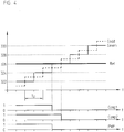
- the FIG. 4 shows that with two counter ramps Codd, Ceven, each with one compared to FIG. 3 halved counting frequency or a doubled counting period Tp count only the odd and even numbers to generate a PWM signal PWM, which is the FIG. 3 completely corresponds.
- the reference value Ref must be compared with the counter readings of each of the two count ramps Codd, Ceven.
- Comparison signals Comp1, Comp2 respectively indicate whether the reference value Ref is greater than the count of the respective count ramp Codd, Ceven. If one connects the two comparison signals Comp1, Comp2 with a logical AND, one obtains therefrom a PWM signal PWM which, like the PWM signal PWM of the FIG. 3 behaves.
- the two counting ramps Codd, Ceven must comply with certain conditions in order to achieve an optimal result. So they have to be shifted against each other by half a counting period Tp.
- PLL P hose L ocked L oop
- Such PLL circuits for generating additional clock signals are already integrated in many FPGAs. The phase position of such a PLL circuit can be easily parameterized and is controlled very precisely.
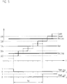
- FIG. 5 Based on FIG. 5 another embodiment will be described. As in the first embodiment, two count ramps Codd, Ceven are used. However, two different reference values Ref_bot and Ref_top for the lower or upper power transistor T of a half-bridge B of the converter U now become off FIG. 1 used. As shown, a dead time Td when switching between the power transistors T can thus be observed in the simplest way.
- the switching timing of the PWM signal PWM_top for the upper power transistor T is earlier than the switching timing of the PWM signal PWM_bot for the lower power transistor.
- the PWM signal PWM_top was obtained with the same logic as the PWM signal PWM FIG. 4 , It is then at a high level if the reference value Ref_top is greater than the count each of the two counting ramps Codd, Ceven. Accordingly, for the. PWM signal PWM_bot, the reference value PWM_bot is compared with the counter readings of the count ramps Codd, Ceven, and the result of this comparison is additionally inverted. It can be seen that both power transistors T are switched off for a dead time Td. A short circuit of the intermediate circuit voltage of the converter U by delayed responding power semiconductors T is thus excluded.
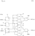
- FIG. 6 shows a block diagram of the logic, with the second embodiment according to FIG. 5 can be implemented.
- Two counters C1 and C2 are clocked at 150 MHz.
- the counter C1 counts the count ramp Codd
- the counter C2 counts the count ramp Ceven of FIG. 5
- Both counters are offset by half a counting period.
- a logic module L receives a reference value Ref and generates therefrom the two reference values Ref_bot and Ref_top of FIG. 5 ,
- the mean value of the two reference values Ref_bot and Ref_top corresponds precisely to the original reference value Ref, which is proportional to a required voltage at an output of the half-bridge (B). In this way, the dead time Td is distributed symmetrically around the original switching time.
- a comparator K1 checks whether the reference value Ref_top is greater than the count of C1.
- a comparator K2 checks whether the reference value Ref_top is greater than the count of C2.
- the outputs of the two comparators K1, K2 result in a logical AND associated with the PWM signal PWM_top for driving the upper power transistor T of a half-bridge.
- a comparator K3 checks whether the reference value Ref_bot is greater than the count of C1.
- a comparator K4 checks whether the reference value Ref_bot is greater than the count of C2.
- the outputs of the two comparators K3, K4 result in a logical NAND (NAND) linked to the PWM signal PWM_bot for driving the lower power transistor T of a half-bridge.
- Both embodiments shown here allow the generation of PWM signals for driving the power transistors in a converter, wherein a reference value with 10-bit resolution is compared against a counter with also 10-bit resolution at a count frequency of 295 MHz. This succeeds, although internally only one clock of approx. 150 MHz is available.
- the PWM signals for the upper and lower power transistor of a half-bridge are generated in a converter so that the dead time is maintained when switching between the two power semiconductors, without further measures would be necessary.
- condition "reference value is greater than count” is used in the above exemplary embodiments and in the claims, then this means either the condition “is greater”, or alternatively the condition “is greater than or equal to”, because whether equality of Reference value and counter reading
- the corresponding PWM signal is at a high level or at a low level, is irrelevant and can be set as desired.
Landscapes
- Inverter Devices (AREA)
Claims (6)
- Procédé pour générer un signal PWM destiné à commander les transistors de puissance (T) d'un demi-pont (B) d'un convertisseur (U) au moyen d'un circuit numérique (FPGA), après qu'une valeur de référence numérique (Ref) a été comparée à l'état d'un compteur d'une rampe de comptage numérique (C), dans lequel un état logique du signal PWM (PWM) dépend du fait que la valeur de référence (Ref) est ou non supérieure à l'état de compteur de la rampe de comptage (C), caractérisé en ce qu'au moins deux compteurs (C1, C2) comptent des états de compteur alternativement consécutifs de la rampe de comptage (C), et en ce que l'état logique du signal PWM (PWM) dépend du fait que la valeur de référence (Ref) est ou non supérieure à l'état de compteur de rampes de comptage (Codd, Ceven) des au moins deux compteurs (C1, C2).
- Procédé selon la revendication 1, caractérisé en ce que deux compteurs (C1, C2) comptent avec des périodes de comptage (Tp) identiques décalées d'une moitié de période de comptage (Tp).
- Procédé selon la revendication 1 ou 2, caractérisé en ce que, au niveau d'un point d'inflexion supérieur ou inférieur des rampes de comptage (Codd, Ceven) comptant selon un trajet triangulaire, le compteur (C1, C2) qui atteint en dernier son point d'inflexion quitte de nouveau ce dernier en tant que premier.
- Procédé selon l'une quelconque des revendications précédentes, caractérisé en ce qu'une plage de valeurs de la valeur de référence (Ref, Ref_bot, Ref_top) est inférieure à une plage de valeurs des au moins deux compteurs (C1, C2).
- Procédé selon l'une quelconque des revendications précédentes, caractérisé en ce que, pour chacun des deux transistors de puissance (T) du demi-pont (B), une valeur de référence propre (Ref_bot, Ref_top) est soumise à une comparaison avec les états de compteur des rampes de comptage (Codd, Ceven) de manière à ce que les signaux PWM obtenus (PWM_bot, PWM_top) contiennent un temps mort (Td).
- Procédé selon l'une quelconque des revendications précédentes, caractérisé en ce que, pour chacun des deux transistors de puissance (T) du demi-pont (B), des valeurs de référence propres (Ref_bot, Ref_top) soient situées de manière symétrique par rapport à la valeur de référence (Ref), qui est proportionnelle à une tension requise à une sortie du demi-pont (B).
Applications Claiming Priority (1)
| Application Number | Priority Date | Filing Date | Title |
|---|---|---|---|
| DE102007048439A DE102007048439A1 (de) | 2007-10-09 | 2007-10-09 | Verfahren zum Erzeugen von PWM-Signalen |
Publications (3)
| Publication Number | Publication Date |
|---|---|
| EP2048778A2 EP2048778A2 (fr) | 2009-04-15 |
| EP2048778A3 EP2048778A3 (fr) | 2014-01-15 |
| EP2048778B1 true EP2048778B1 (fr) | 2017-05-03 |
Family
ID=40262036
Family Applications (1)
| Application Number | Title | Priority Date | Filing Date |
|---|---|---|---|
| EP08012263.3A Active EP2048778B1 (fr) | 2007-10-09 | 2008-07-08 | Procédé de production de signaux PWM |
Country Status (3)
| Country | Link |
|---|---|
| US (1) | US7692465B2 (fr) |
| EP (1) | EP2048778B1 (fr) |
| DE (1) | DE102007048439A1 (fr) |
Families Citing this family (2)
| Publication number | Priority date | Publication date | Assignee | Title |
|---|---|---|---|---|
| CH703739A2 (fr) | 2010-08-31 | 2012-03-15 | Etel Sa | Circuit de commande d'un moteur électrique avec un asservissement du courant d'alimentation. |
| EP4120559B1 (fr) * | 2021-07-14 | 2024-02-28 | Etel S.A. | Procédé de commande pwm pour moteur électrique avec compensation de passage à zéro |
Family Cites Families (10)
| Publication number | Priority date | Publication date | Assignee | Title |
|---|---|---|---|---|
| DE3373250D1 (en) * | 1982-06-15 | 1987-10-01 | Toshiba Kk | Pulse-width modulation circuit |
| JP3001623B2 (ja) * | 1990-10-23 | 2000-01-24 | 松下電器産業株式会社 | Pwm型d/a変換器 |
| DE69813843D1 (de) * | 1998-12-23 | 2003-05-28 | St Microelectronics Srl | Umwandlung von einem numerischen Befehlswert in ein Pulsbreitenmodulationsantriebsignal mit konstanter Frequenz für eine elektromagnetische Last |
| DE19920306B4 (de) * | 1999-05-03 | 2008-02-28 | Stmicroelectronics Gmbh | Schaltungsvorrichtung zum Regeln des Stroms durch eine induktive Last |
| JP2004357450A (ja) * | 2003-05-30 | 2004-12-16 | Matsushita Electric Ind Co Ltd | Pwm回路およびマイクロコントローラ |
| JP4681830B2 (ja) * | 2004-06-24 | 2011-05-11 | パナソニック株式会社 | Pwm回路およびpwm回路制御方法 |
| US7453250B2 (en) * | 2005-02-10 | 2008-11-18 | Intersil Americas Inc. | PWM controller with dual-edge modulation using dual ramps |
| JP4760909B2 (ja) * | 2005-09-13 | 2011-08-31 | トヨタ自動車株式会社 | Pwm信号生成回路 |
| DE102005061388A1 (de) | 2005-12-02 | 2007-06-06 | Dr. Johannes Heidenhain Gmbh | Pulsweitenmodulationsverfahren |
| US7459951B2 (en) * | 2006-02-22 | 2008-12-02 | Exar Corporation | Self-calibrating digital pulse-width modulator (DPWM) |
-
2007
- 2007-10-09 DE DE102007048439A patent/DE102007048439A1/de not_active Withdrawn
-
2008
- 2008-07-08 EP EP08012263.3A patent/EP2048778B1/fr active Active
- 2008-10-06 US US12/246,201 patent/US7692465B2/en not_active Expired - Fee Related
Also Published As
| Publication number | Publication date |
|---|---|
| EP2048778A2 (fr) | 2009-04-15 |
| US7692465B2 (en) | 2010-04-06 |
| DE102007048439A1 (de) | 2009-04-16 |
| US20090091365A1 (en) | 2009-04-09 |
| EP2048778A3 (fr) | 2014-01-15 |
Similar Documents
| Publication | Publication Date | Title |
|---|---|---|
| EP2269295B1 (fr) | Procede de détermination d'un vecteur polaire de courant, redresseur, carte de circuits et serie de redresseurs | |
| EP2730019B1 (fr) | Procédé pour faire fonctionner un onduleur et onduleur tolérant aux pannes de secteur | |
| DE102015108822A1 (de) | System und Verfahren zum Stromabtasten in einem Schaltnetzteil | |
| DE102016100438A1 (de) | Leistungs-Stromrichter mit Vorkompensation für Totzeiteneinsatz | |
| DE112014003998T5 (de) | Wechselrichtervorrichtung | |
| DE102017127780A1 (de) | Adaptive Impulsbreitenmodulation bei Motorsteuerungssystemen | |
| DE112013005939T5 (de) | Wandlergerät | |
| DE102009027263A1 (de) | Geschwindigkeitserkennung zur Halbbrücken-Steuerung | |
| EP2294686B1 (fr) | Procédé et dispositif pour générer des signaux mli | |
| DE102016100440A1 (de) | Leistungswandler mit Totzeitvariation zum Streuen einer Verzerrung | |
| WO2003041258A2 (fr) | Convertisseur et procede pour determiner un indicateur spatial de courant | |
| EP2048778B1 (fr) | Procédé de production de signaux PWM | |
| DE10112820A1 (de) | Verfahren zur Messung von Strömen in Multiphasenwandlern mit Strommesselement-Auslösung | |
| DE102020124345A1 (de) | System und Verfahren zum Überwachen eines Schaltnetzteils | |
| EP1936789A2 (fr) | Circuit de delai pour un convertisseur MLI | |
| EP3369167B1 (fr) | Unité de récupération d'énergie et système d'entraînement électrique | |
| DE102017128602A1 (de) | Verfahren zum Bestimmen der Fehlspannung eines Stromrichters sowie Drehfeldmaschine mit Fehlspannungskompensation | |
| EP3285381A1 (fr) | Procédé de fonctionnement d'une machine électrique et machine électrique | |
| DE10110615A1 (de) | Verfahren zur Erzeugung von Ansteuerimpulsen für Leistungshalbleiter | |
| EP2254233B1 (fr) | Procédé de fonctionnement d'un circuit convertisseur ainsi que dispositif destiné à l'exécution du procédé | |
| EP3039786B1 (fr) | Circuit et procédé de génération d'un signal de sortie à rapport cyclique variable | |
| EP3619804B1 (fr) | Procédé de commande d'un convertisseur de courant, dispositif de commande pour un convertisseur de courant et convertisseur de courant | |
| EP2409394B1 (fr) | Procédé de fonctionnement d'un circuit convertisseur et dispositif pour la mise en uvre du procédé | |
| EP2945288A1 (fr) | Circuit et procédé de commande d'un élément commutateur de semi-conducteur | |
| DE102019218940A1 (de) | Dreiphasen-wechselstromsteuervorrichtung und dreiphasen-wechselstromsteuersystem |
Legal Events
| Date | Code | Title | Description |
|---|---|---|---|
| PUAI | Public reference made under article 153(3) epc to a published international application that has entered the european phase |
Free format text: ORIGINAL CODE: 0009012 |
|
| AK | Designated contracting states |
Kind code of ref document: A2 Designated state(s): AT BE BG CH CY CZ DE DK EE ES FI FR GB GR HR HU IE IS IT LI LT LU LV MC MT NL NO PL PT RO SE SI SK TR |
|
| AX | Request for extension of the european patent |
Extension state: AL BA MK RS |
|
| PUAL | Search report despatched |
Free format text: ORIGINAL CODE: 0009013 |
|
| AK | Designated contracting states |
Kind code of ref document: A3 Designated state(s): AT BE BG CH CY CZ DE DK EE ES FI FR GB GR HR HU IE IS IT LI LT LU LV MC MT NL NO PL PT RO SE SI SK TR |
|
| AX | Request for extension of the european patent |
Extension state: AL BA MK RS |
|
| RIC1 | Information provided on ipc code assigned before grant |
Ipc: H03K 7/08 20060101AFI20131209BHEP |
|
| 17P | Request for examination filed |
Effective date: 20140715 |
|
| RBV | Designated contracting states (corrected) |
Designated state(s): AT BE BG CH CY CZ DE DK EE ES FI FR GB GR HR HU IE IS IT LI LT LU LV MC MT NL NO PL PT RO SE SI SK TR |
|
| AKX | Designation fees paid |
Designated state(s): AT BE BG CH CY CZ DE DK EE ES FI FR GB GR HR HU IE IS IT LI LT LU LV MC MT NL NO PL PT RO SE SI SK TR |
|
| GRAP | Despatch of communication of intention to grant a patent |
Free format text: ORIGINAL CODE: EPIDOSNIGR1 |
|
| INTG | Intention to grant announced |
Effective date: 20170117 |
|
| GRAS | Grant fee paid |
Free format text: ORIGINAL CODE: EPIDOSNIGR3 |
|
| GRAA | (expected) grant |
Free format text: ORIGINAL CODE: 0009210 |
|
| AK | Designated contracting states |
Kind code of ref document: B1 Designated state(s): AT BE BG CH CY CZ DE DK EE ES FI FR GB GR HR HU IE IS IT LI LT LU LV MC MT NL NO PL PT RO SE SI SK TR |
|
| REG | Reference to a national code |
Ref country code: GB Ref legal event code: FG4D Free format text: NOT ENGLISH |
|
| REG | Reference to a national code |
Ref country code: AT Ref legal event code: REF Ref document number: 891032 Country of ref document: AT Kind code of ref document: T Effective date: 20170515 Ref country code: CH Ref legal event code: EP |
|
| REG | Reference to a national code |
Ref country code: CH Ref legal event code: NV Representative=s name: ICB INGENIEURS CONSEILS EN BREVETS SA, CH Ref country code: IE Ref legal event code: FG4D Free format text: LANGUAGE OF EP DOCUMENT: GERMAN |
|
| REG | Reference to a national code |
Ref country code: DE Ref legal event code: R096 Ref document number: 502008015265 Country of ref document: DE |
|
| REG | Reference to a national code |
Ref country code: NL Ref legal event code: FP |
|
| REG | Reference to a national code |
Ref country code: LT Ref legal event code: MG4D |
|
| PG25 | Lapsed in a contracting state [announced via postgrant information from national office to epo] |
Ref country code: GR Free format text: LAPSE BECAUSE OF FAILURE TO SUBMIT A TRANSLATION OF THE DESCRIPTION OR TO PAY THE FEE WITHIN THE PRESCRIBED TIME-LIMIT Effective date: 20170804 Ref country code: FI Free format text: LAPSE BECAUSE OF FAILURE TO SUBMIT A TRANSLATION OF THE DESCRIPTION OR TO PAY THE FEE WITHIN THE PRESCRIBED TIME-LIMIT Effective date: 20170503 Ref country code: ES Free format text: LAPSE BECAUSE OF FAILURE TO SUBMIT A TRANSLATION OF THE DESCRIPTION OR TO PAY THE FEE WITHIN THE PRESCRIBED TIME-LIMIT Effective date: 20170503 Ref country code: NO Free format text: LAPSE BECAUSE OF FAILURE TO SUBMIT A TRANSLATION OF THE DESCRIPTION OR TO PAY THE FEE WITHIN THE PRESCRIBED TIME-LIMIT Effective date: 20170803 Ref country code: LT Free format text: LAPSE BECAUSE OF FAILURE TO SUBMIT A TRANSLATION OF THE DESCRIPTION OR TO PAY THE FEE WITHIN THE PRESCRIBED TIME-LIMIT Effective date: 20170503 Ref country code: HR Free format text: LAPSE BECAUSE OF FAILURE TO SUBMIT A TRANSLATION OF THE DESCRIPTION OR TO PAY THE FEE WITHIN THE PRESCRIBED TIME-LIMIT Effective date: 20170503 |
|
| PG25 | Lapsed in a contracting state [announced via postgrant information from national office to epo] |
Ref country code: LV Free format text: LAPSE BECAUSE OF FAILURE TO SUBMIT A TRANSLATION OF THE DESCRIPTION OR TO PAY THE FEE WITHIN THE PRESCRIBED TIME-LIMIT Effective date: 20170503 Ref country code: BG Free format text: LAPSE BECAUSE OF FAILURE TO SUBMIT A TRANSLATION OF THE DESCRIPTION OR TO PAY THE FEE WITHIN THE PRESCRIBED TIME-LIMIT Effective date: 20170803 Ref country code: SE Free format text: LAPSE BECAUSE OF FAILURE TO SUBMIT A TRANSLATION OF THE DESCRIPTION OR TO PAY THE FEE WITHIN THE PRESCRIBED TIME-LIMIT Effective date: 20170503 Ref country code: IS Free format text: LAPSE BECAUSE OF FAILURE TO SUBMIT A TRANSLATION OF THE DESCRIPTION OR TO PAY THE FEE WITHIN THE PRESCRIBED TIME-LIMIT Effective date: 20170903 Ref country code: PL Free format text: LAPSE BECAUSE OF FAILURE TO SUBMIT A TRANSLATION OF THE DESCRIPTION OR TO PAY THE FEE WITHIN THE PRESCRIBED TIME-LIMIT Effective date: 20170503 |
|
| PG25 | Lapsed in a contracting state [announced via postgrant information from national office to epo] |
Ref country code: EE Free format text: LAPSE BECAUSE OF FAILURE TO SUBMIT A TRANSLATION OF THE DESCRIPTION OR TO PAY THE FEE WITHIN THE PRESCRIBED TIME-LIMIT Effective date: 20170503 Ref country code: CZ Free format text: LAPSE BECAUSE OF FAILURE TO SUBMIT A TRANSLATION OF THE DESCRIPTION OR TO PAY THE FEE WITHIN THE PRESCRIBED TIME-LIMIT Effective date: 20170503 Ref country code: DK Free format text: LAPSE BECAUSE OF FAILURE TO SUBMIT A TRANSLATION OF THE DESCRIPTION OR TO PAY THE FEE WITHIN THE PRESCRIBED TIME-LIMIT Effective date: 20170503 Ref country code: SK Free format text: LAPSE BECAUSE OF FAILURE TO SUBMIT A TRANSLATION OF THE DESCRIPTION OR TO PAY THE FEE WITHIN THE PRESCRIBED TIME-LIMIT Effective date: 20170503 Ref country code: RO Free format text: LAPSE BECAUSE OF FAILURE TO SUBMIT A TRANSLATION OF THE DESCRIPTION OR TO PAY THE FEE WITHIN THE PRESCRIBED TIME-LIMIT Effective date: 20170503 |
|
| REG | Reference to a national code |
Ref country code: DE Ref legal event code: R097 Ref document number: 502008015265 Country of ref document: DE |
|
| PG25 | Lapsed in a contracting state [announced via postgrant information from national office to epo] |
Ref country code: IT Free format text: LAPSE BECAUSE OF FAILURE TO SUBMIT A TRANSLATION OF THE DESCRIPTION OR TO PAY THE FEE WITHIN THE PRESCRIBED TIME-LIMIT Effective date: 20170503 |
|
| PLBE | No opposition filed within time limit |
Free format text: ORIGINAL CODE: 0009261 |
|
| STAA | Information on the status of an ep patent application or granted ep patent |
Free format text: STATUS: NO OPPOSITION FILED WITHIN TIME LIMIT |
|
| 26N | No opposition filed |
Effective date: 20180206 |
|
| REG | Reference to a national code |
Ref country code: IE Ref legal event code: MM4A |
|
| GBPC | Gb: european patent ceased through non-payment of renewal fee |
Effective date: 20170803 |
|
| REG | Reference to a national code |
Ref country code: FR Ref legal event code: ST Effective date: 20180330 |
|
| PG25 | Lapsed in a contracting state [announced via postgrant information from national office to epo] |
Ref country code: IE Free format text: LAPSE BECAUSE OF NON-PAYMENT OF DUE FEES Effective date: 20170708 |
|
| PG25 | Lapsed in a contracting state [announced via postgrant information from national office to epo] |
Ref country code: SI Free format text: LAPSE BECAUSE OF FAILURE TO SUBMIT A TRANSLATION OF THE DESCRIPTION OR TO PAY THE FEE WITHIN THE PRESCRIBED TIME-LIMIT Effective date: 20170503 Ref country code: FR Free format text: LAPSE BECAUSE OF NON-PAYMENT OF DUE FEES Effective date: 20170731 |
|
| REG | Reference to a national code |
Ref country code: BE Ref legal event code: MM Effective date: 20170731 |
|
| PG25 | Lapsed in a contracting state [announced via postgrant information from national office to epo] |
Ref country code: LU Free format text: LAPSE BECAUSE OF NON-PAYMENT OF DUE FEES Effective date: 20170708 |
|
| PG25 | Lapsed in a contracting state [announced via postgrant information from national office to epo] |
Ref country code: GB Free format text: LAPSE BECAUSE OF NON-PAYMENT OF DUE FEES Effective date: 20170803 |
|
| PG25 | Lapsed in a contracting state [announced via postgrant information from national office to epo] |
Ref country code: BE Free format text: LAPSE BECAUSE OF NON-PAYMENT OF DUE FEES Effective date: 20170731 |
|
| PG25 | Lapsed in a contracting state [announced via postgrant information from national office to epo] |
Ref country code: MT Free format text: LAPSE BECAUSE OF FAILURE TO SUBMIT A TRANSLATION OF THE DESCRIPTION OR TO PAY THE FEE WITHIN THE PRESCRIBED TIME-LIMIT Effective date: 20170503 |
|
| PG25 | Lapsed in a contracting state [announced via postgrant information from national office to epo] |
Ref country code: MC Free format text: LAPSE BECAUSE OF FAILURE TO SUBMIT A TRANSLATION OF THE DESCRIPTION OR TO PAY THE FEE WITHIN THE PRESCRIBED TIME-LIMIT Effective date: 20170503 Ref country code: HU Free format text: LAPSE BECAUSE OF FAILURE TO SUBMIT A TRANSLATION OF THE DESCRIPTION OR TO PAY THE FEE WITHIN THE PRESCRIBED TIME-LIMIT; INVALID AB INITIO Effective date: 20080708 |
|
| PG25 | Lapsed in a contracting state [announced via postgrant information from national office to epo] |
Ref country code: CY Free format text: LAPSE BECAUSE OF NON-PAYMENT OF DUE FEES Effective date: 20170503 |
|
| PG25 | Lapsed in a contracting state [announced via postgrant information from national office to epo] |
Ref country code: TR Free format text: LAPSE BECAUSE OF FAILURE TO SUBMIT A TRANSLATION OF THE DESCRIPTION OR TO PAY THE FEE WITHIN THE PRESCRIBED TIME-LIMIT Effective date: 20170503 |
|
| PG25 | Lapsed in a contracting state [announced via postgrant information from national office to epo] |
Ref country code: PT Free format text: LAPSE BECAUSE OF FAILURE TO SUBMIT A TRANSLATION OF THE DESCRIPTION OR TO PAY THE FEE WITHIN THE PRESCRIBED TIME-LIMIT Effective date: 20170503 |
|
| PGFP | Annual fee paid to national office [announced via postgrant information from national office to epo] |
Ref country code: NL Payment date: 20230719 Year of fee payment: 16 |
|
| PGFP | Annual fee paid to national office [announced via postgrant information from national office to epo] |
Ref country code: CH Payment date: 20230801 Year of fee payment: 16 Ref country code: AT Payment date: 20230720 Year of fee payment: 16 |
|
| PGFP | Annual fee paid to national office [announced via postgrant information from national office to epo] |
Ref country code: DE Payment date: 20230719 Year of fee payment: 16 |