EP3985877A1 - Systeme und verfahren zur verarbeitung von fehlern in digitalen strahlformungsempfängern - Google Patents
Systeme und verfahren zur verarbeitung von fehlern in digitalen strahlformungsempfängern Download PDFInfo
- Publication number
- EP3985877A1 EP3985877A1 EP21200915.3A EP21200915A EP3985877A1 EP 3985877 A1 EP3985877 A1 EP 3985877A1 EP 21200915 A EP21200915 A EP 21200915A EP 3985877 A1 EP3985877 A1 EP 3985877A1
- Authority
- EP
- European Patent Office
- Prior art keywords
- adcs
- errors
- sub
- error
- adc
- Prior art date
- Legal status (The legal status is an assumption and is not a legal conclusion. Google has not performed a legal analysis and makes no representation as to the accuracy of the status listed.)
- Withdrawn
Links
Images


Classifications
-
- G—PHYSICS
- G01—MEASURING; TESTING
- G01S—RADIO DIRECTION-FINDING; RADIO NAVIGATION; DETERMINING DISTANCE OR VELOCITY BY USE OF RADIO WAVES; LOCATING OR PRESENCE-DETECTING BY USE OF THE REFLECTION OR RERADIATION OF RADIO WAVES; ANALOGOUS ARRANGEMENTS USING OTHER WAVES
- G01S7/00—Details of systems according to groups G01S13/00, G01S15/00, G01S17/00
- G01S7/02—Details of systems according to groups G01S13/00, G01S15/00, G01S17/00 of systems according to group G01S13/00
- G01S7/40—Means for monitoring or calibrating
- G01S7/4004—Means for monitoring or calibrating of parts of a radar system
- G01S7/4021—Means for monitoring or calibrating of parts of a radar system of receivers
-
- H—ELECTRICITY
- H03—ELECTRONIC CIRCUITRY
- H03M—CODING; DECODING; CODE CONVERSION IN GENERAL
- H03M1/00—Analogue/digital conversion; Digital/analogue conversion
- H03M1/10—Calibration or testing
- H03M1/1009—Calibration
- H03M1/1033—Calibration over the full range of the converter, e.g. for correcting differential non-linearity
-
- G—PHYSICS
- G06—COMPUTING OR CALCULATING; COUNTING
- G06F—ELECTRIC DIGITAL DATA PROCESSING
- G06F7/00—Methods or arrangements for processing data by operating upon the order or content of the data handled
- G06F7/22—Arrangements for sorting or merging computer data on continuous record carriers, e.g. tape, drum, disc
- G06F7/24—Sorting, i.e. extracting data from one or more carriers, rearranging the data in numerical or other ordered sequence, and rerecording the sorted data on the original carrier or on a different carrier or set of carriers sorting methods in general
-
- H—ELECTRICITY
- H03—ELECTRONIC CIRCUITRY
- H03M—CODING; DECODING; CODE CONVERSION IN GENERAL
- H03M1/00—Analogue/digital conversion; Digital/analogue conversion
- H03M1/12—Analogue/digital converters
- H03M1/124—Sampling or signal conditioning arrangements specially adapted for A/D converters
- H03M1/1245—Details of sampling arrangements or methods
-
- G—PHYSICS
- G01—MEASURING; TESTING
- G01S—RADIO DIRECTION-FINDING; RADIO NAVIGATION; DETERMINING DISTANCE OR VELOCITY BY USE OF RADIO WAVES; LOCATING OR PRESENCE-DETECTING BY USE OF THE REFLECTION OR RERADIATION OF RADIO WAVES; ANALOGOUS ARRANGEMENTS USING OTHER WAVES
- G01S7/00—Details of systems according to groups G01S13/00, G01S15/00, G01S17/00
- G01S7/02—Details of systems according to groups G01S13/00, G01S15/00, G01S17/00 of systems according to group G01S13/00
- G01S7/027—Constructional details of housings, e.g. form, type, material or ruggedness
-
- H—ELECTRICITY
- H03—ELECTRONIC CIRCUITRY
- H03M—CODING; DECODING; CODE CONVERSION IN GENERAL
- H03M1/00—Analogue/digital conversion; Digital/analogue conversion
- H03M1/12—Analogue/digital converters
- H03M1/1205—Multiplexed conversion systems
- H03M1/121—Interleaved, i.e. using multiple converters or converter parts for one channel
- H03M1/1215—Interleaved, i.e. using multiple converters or converter parts for one channel using time-division multiplexing
Definitions
- Digital beamforming receivers utilize a large array of analog-to-converters (ADCs) to process broadband signals ranging from hundreds of megahertz (MHz) to multiple gigahertz (GHz) with moderate to high resolution, e.g., 8-12 bits.
- ADCs should operate synchronously with minimal timing errors in order to produce reliable digital output.
- time-interleaved ADC architectures are often used for analog-to-digital conversion.
- a time-interleaved ADC is an ADC that uses multiple sub-ADCs that sample at different time instances. Utilization of time-interleaved ADCs results in a sampling rate increase proportional to the number of sub-ADCs used. Due to the increased number of sub-ADCs utilized for digital beamforming, additional mismatch error occurs between the sub-ADCs. The result is that the signal at the ADC is corrupted by signal errors resulting in unwanted output at the output of the digital beamforming receiver system.
- FIGs. 1-3 illustrate a wireless system having a digital beamforming receiver in accordance with some embodiments.
- an error correction system in the digital beamforming receiver is configured to reduce the amount of error that occurs in the digital beamforming receiver when signals are sampled by analog-to-digital converters (ADCs).
- the ADCs may be, for example, time-interleaving ADCs that are designed to utilize sub-ADCs to perform sampling operations in tandem.
- an error correction system dynamically adjusts the sequence of sampling operations such that the sequence of sampling operations corresponds to a reduction in the number of errors in the ADCs.
- the error correction system receives sampled signals from sub-ADCs of the ADCs, detects the errors associated with each sub-ADC, and uses the detected errors to generate an error matrix that is reconfigured such that a summation of the errors in each column approximates to the summation of errors of other columns of the reconfigured matrix.
- the error correction system uses the reconfigured error matrix to generate a sequence of sample operations for the sub-ADCs that correspond to the minimized errors associated with the reconfigured matrix.
- the newly created sequence of sample operations are used to sequence the sub-ADCs of the time-interleaving ADCs. Sampling according to the newly generated sequence of sampling operations allows the digital beamforming system to reduce the amount of errors generated when sampling additional signals received by the digital beamforming system.
- FIG. 1 illustrates a wireless system 100 in accordance with some embodiments.
- the wireless system may be, for example, a Radio Detection And Ranging (RADAR) system.
- the wireless system 100 includes a transmitter 102 and a digital beamforming receiver 105 according to some embodiments.
- Digital beamforming receiver 105 includes a receiver front-end 110, analog-to-digital-converters (ADCs) 120, an interface 130, a digital processing unit 140, an error identification unit 150, a selection unit 160, a clock and sub-ADC selection logic unit 170.
- ADCs analog-to-digital-converters
- digital processing unit 140 is configured to perform beamforming operations or functions.
- ADC 120 includes time-interleaved analog-to-digital converters (TI-ADC) 122 - 1 - 122 - N.
- TI-ADC 122-1 includes sub-ADCs 132-1 - 132-M.
- TI-ADC 122-2 includes sub-ADCs 133-1 - 133-M.
- TI-ADC 122-N includes sub-ADCs 134-1 - 134-M.
- receiver front-end 110 is coupled to ADCs 120.
- ADCs 120 are coupled to an interface 130 and clock and sub-ADC selection logic unit 170.
- Interface 130 is coupled to error identification unit 150.
- Error identification unit 150 is coupled to selection unit 160.
- Selection unit 160 is coupled to clock and sub-ADC selection logic unit 170.
- the interface 130 is, for example, a memory or registers that store the data incoming from ADCs 120.
- the number of antenna inputs to the receiver front-end 110 is equal to the number N of ADC inputs or fewer than N for the case of a hybrid/analog digital beamforming system.
- receiver front-end 110 of digital beamforming receiver 105 receives transmission signals (radio frequency (RF) signals or millimeter wave signals) originating from a transmitter (not shown) and converts the signals to intermediate frequency (IF) signals.
- RF radio frequency
- IF intermediate frequency
- receiver front-end 110 provides the IF signals to each sub-ADC 132, sub-ADC 133 and sub-ADC 134 of TI-ADC 122 for sampling.
- the number of sub-ADCs and TI-ADCs that are used to sample the IF signals may vary depending on, for example, the number of sub-ADCs and TI-ADCs required to perform sampling operations.
- TI-ADC 122 receives the input IF signals and commences the process of using the sub-ADCs of the time-interleaving ADCs to sample and convert the IF signals to digital form.
- the input IF signal received by TI-ADC 122-1 is sampled by each sub-ADC 132-1 - 132-M.
- the input IF signal received by TI-ADC 122-2 is sampled by each sub-ADC 133-1 - 133-M.
- the input IF signal received by TI-ADC 122-N is sampled by each sub-ADC 134-1 - 134-M.
- the first sub-ADC 132-1 of TI-ADC 122-1, the first sub-ADC 133-1 of TI-ADC 122-2, and the first sub-ADC 134-1 are configured to simultaneously sample the input IF signal.
- the second sub-ADC 132-2 of TI-ADC 122-1, the second sub-ADC 133-2 of TI-ADC 122-2, and the second sub-ADC 134-2 are configured to simultaneously sample the input IF signal.
- the third sub-ADC 132-3 of TI-ADC 122-1, the third sub-ADC 133-3 of TI-ADC 122-2, and the third sub-ADC 134-3 are configured to simultaneously sample the input IF signal.
- the TI-ADCs 122 of ADC 120 provide the sampled output from the sub-ADCs 132, sub-ADCs 133, and sub-ADCs 134 to error identification unit 150.
- the error identification unit 150 receives the sampled output signals from digital processing unit 140 or from each sub-ADC 132, sub-ADC 133, and sub-ADC 134 of TI-ADCs 122 and identifies errors in the received sampled signals. Typical correlation and averaging processing techniques known in the art are used to identify the errors. In some embodiments the errors identified are associated with each sub-ADC (e.g., timing, offset, and gain) and/or with digital processing unit 140 (e.g. spectral images, ghost errors, or spurs). That is, in some embodiments, digital processing unit 140 generates digitally beamformed data from sampled output 114, but the digitally beamformed data includes, for example, sub-ADC errors.
- each sub-ADC e.g., timing, offset, and gain
- digital processing unit 140 e.g. spectral images, ghost errors, or spurs. That is, in some embodiments, digital processing unit 140 generates digitally beamformed data from sampled output 114, but the digitally beamformed data
- digital processing unit 140 delivers its output to error identification unit 150 for purposes of identifying spectral images instead of or in addition to individual sub-ADC errors.
- error identification unit 150 generates an error matrix or table, T, that includes the identified errors (e.g., timing errors, offset errors, spectral images, ghost errors, or spurs etc.) of the sub-ADCs sub-ADC 132, sub-ADC 133, and sub-ADC 134 in the TI-ADCs 122.
- each row in the table T represents the errors of the sub-ADCs for a single TI-ADC 122.
- T11 which is the first column in the first row of the table, is the timing error of the first sub-ADC 132-1 of the first time interleave ADC, i.e., TI-ADC 122-1.
- T12 is the timing error of the second sub-ADC 132-2 of TI-ADC 122-1, etc.
- T21 is the timing error of the first sub-ADC 133-1 of the second time interleave ADC, i.e., TI-ADC 122-2.
- T22 is the timing error of the second sub-ADC 133-2 of TI-ADC 122-2, etc.
- selection unit 160 receives the error matrix T from error identification unit 150 and sorts the error matrix T from minimum-to-maximum to generate a matrix S. That is, after the timing errors have been stored in matrix T, selection unit 160 uses a sort function to process the errors into a sorted matrix S. In some embodiments, the sorting function that is used in the error correction process is a minimum-error-to-maximum error sorting function. After generating the sorted matrix S, selection unit 160 provides the sorted matrix S to clock and sub-ADC selection unit 170.
- clock and sub-ADC selection unit 170 receives the sorted matrix S and uses a cost function to position the elements within the same row of matrix S into a matrix C in such that when the values of each column in matrix C are summed, the sum of each column of matrix C is within a predefined target value.
- the predefined target value is defined such that the sum of each column in is approximately identical.
- the cost function positions the elements within the same row of matrix C in such an order such that when the values of each column are summed, the sum of each column are exactly identical.
- clock and sub-ADC selection unit 170 is able to pair the sub-ADCs that have minimum errors with the sub-ADCs that have maximum errors such that the summation of the errors in each column approximate to each other.
- Clock and sub-ADC selection unit 170 uses the pairing to sequence the sampling operations of the sub-ADCs that have been mapped to the error elements in reconfigured matrix C.
- clock and sub-ADC selection logic unit 170 uses a barrel-shifter function to pair the sub-ADCs with minimum errors with sub-ADCs that have maximum errors.
- clock and sub-ADC selection unit 170 barrel-shifts to the last row as many columns as there are in matrix S, the maximum error sub-ADC is paired with the minimum error sub-ADC of the time interleave ADC.
- the TI-ADCs of ADC 120 are programmed by clock and sub-ADC selection logic unit 170 such that the maximum error sub-ADC samples at the same time as the minimum error sub-ADC of time interleave ADC.
- the paired sequence of operations is provided by clock and sub-ADC selection logic unit 170 to TI-ADCs 122 as programming for the sub-ADCs, which then sample according to the updated pair sequence of operations.
- FIG. 2 depicts an error correction system 243 of digital beamforming receiver 105 of FIG. 1 in accordance with some embodiments.
- the error correction system 243 includes error identification unit 150, selection unit 160, and clock and sub-ADC selection logic unit 170.
- error identification unit 150 receives the sampled output 114 from sub-ADCs 132, sub-ADCs 133, and sub-ADCs 134 of TI-ADCs 122 and identifies the errors in the processed output in order to generate the error matrix 251 (T), sorted matrix 261 (S), and cost matrix 271 (C).
- the matrices T, S, and C are used to optimize the sequence of sampling operations of the sub-ADCs 132-1.
- the matrix T is a matrix that represents errors caused by the sub-ADCs 132.
- the elements in matrix T represent a timing error that is a difference in the ideal sampling time and the actual sampling time of sub-ADCs 132.
- the matrix S is a matrix that is used to sort the errors captured in matrix T from minimum to maximum.
- Matrix C is a matrix that is used to rearrange the error values in S using, for example, a barrel shifter function, such that the summation of each column C approximates in value to the summation of other columns in C.
- the TI-ADCs 122 sample every Ts/M sequentially with the sub-ADCs 132 in each column. For example, in one embodiment, error identification unit 150 determines that the third sub-ADC 132-3 of the first TI-ADC 122-1 has a timing error t 1,3 seconds compared to an ideal moment or sampling instance. In some embodiments, the ideal sampling instances for each sub-ADC are stored in, for example, the error identification unit 150. For sampling moments n, n+1, n+2, ... the sub-ADCs in column 1, 2 ... are used respectively. Once the sub-ADCs 132-1 of the last column M is reached, representing the last interleaved sub-ADC of each TI-ADC, the operation commences again from the first column.
- error identification unit 150 stores all the errors in error matrix 251
- selection unit 160 uses a sort function to process the errors into sorted matrix 261.
- the sorted matrix 261 is provided to clock and sub-ADC selection logic unit 170.
- Clock and sub-ADC selection logic unit 170 uses a cost function to position the elements of sorted matrix 261 into cost matrix 271 such that when the values of each column of cost matrix 271 are summed, the sum of each column in cost matrix 271 is approximately identical.
- a deterministic algorithm e.g. sort, inverter sequence and barrel-shifter
- a stochastic algorithm e.g., simulated annealing, neural networks (machine learning) that is trained to optimize the performance when the given performance cost function is known.
- Clock and sub-ADC selection logic unit 170 uses the paired sub-ADCs that yielded the cost matrix 271 to generate the sequence of operations. Clock and sub-ADC selection logic unit 170 receives the optimal sequence of sub-ADC operations from selection unit 160 and programs the sequence of sub-ADCs 132 using a clock and sub-ADC selection logic unit 170.
- Error identification unit 150 receives ADC channel output 22 and measures the magnitude of the mismatch errors (e.g. timing errors, offset errors, gain error, bandwidth error, etc.). The magnitude of each error is placed in matrix T. Error identification unit 150 provides the measured errors in matrix form to selection unit 160.
- Selection unit 160 receives the mismatch errors in the T matrix from error identification unit 150 and, in some embodiments, determines the optimal sequence of sub-ADC operations across the N x M array for each sampling moment using a selection algorithm. In some embodiments, selection unit 160 provides the optimal sequence of sub-ADC operations to a clock and sub-ADC selection logic unit 170.
- a barrel shifter function is adopted as a selection method.
- Matrix C depicts the re-arrangement of the error values based on the barrel shifter function.
- the sorted error values of the first row that refer to the first ADC of the receiver array remain unchanged.
- the first ADC captures the first sample using the sub-ADC with the lowest error.
- the second sample is captured by the sub-ADC with the second lowest error, while the sub-ADC with the largest error is used last in sequence.
- the barrel shifter will shift the error values by one position as seen in the second row of C.
- the sub-ADC introducing the largest error will be used for capturing the first sample and the sub-ADC with the lowest error for the last sample.
- barrel shifter applies two and three positions shift respectively. This action is performed for all the ADC error sets, applying the appropriate shift and resulting in the optimal sequence of sub-ADC sampling operations for the sub-ADCs.
- the position of the error values in C implies the new clocking sequence for each ADC in the array.
- the beamforming operation imports the total error in each sample (that is, across each column) in the array C sum , due to the summation in beamforming function of all samples from all array elements.
- each of the elements in the C sum will approximate the mean value of the distribution.
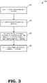
- FIG. 3 is a flow diagram of a method 300 of correcting errors in the radar system of FIG. 1 in accordance with at least one embodiment.
- a plurality of errors associated with sub-ADCs 132 - 134 are identified by an error identification unit 150 and stored in a matrix T.
- the error identification unit 150 identifies or measures a true indication of signal error at the digital beamforming output (e.g., not the timing or offset error but the resulting ghost, image, or spur signal created by it on the input signal when sampled) and subsequently steers the programming of sampling operations to a target sampling sequence that minimizes the true indication of signal error.
- error correction unit 150 forms a error vector with vector dimensions consisting of one or more of a plurality of errors (e.g., a timing error, an offset error, a gain error, a ghost error, and a bandwidth error) and the programming of sampling operations or correction algorithm minimizes the magnitude or phase of the vector errors.
- the selection unit 160 sorts the error values of matrix T from minimum-error-to-maximum-error using a sorting function.
- an optimal sequence of sample operations or pairing of sub-ADCs is selected using, for example, a barrel shifter function or algorithm.
- each error type detected by error identification unit 150 may have an optimal sequence that suppresses that type of error
- a new sequence of sample operations derived from the already captured sequences of operations may provide suppression to all the types of errors detected by the error identification unit 150 simultaneously.
- the new sequence of sampling operations is used to suppress the errors caused by the sub-ADCs 132 - 134 of the TI-ADCs 122.
- certain aspects of the techniques described above may implemented by one or more processors of a processing system executing software.
- the software comprises one or more sets of executable instructions stored or otherwise tangibly embodied on a non-transitory computer readable storage medium.
- the software can include the instructions and certain data that, when executed by the one or more processors, manipulate the one or more processors to perform one or more aspects of the techniques described above.
- the non-transitory computer readable storage medium can include, for example, a magnetic or optical disk storage device, solid state storage devices such as Flash memory, a cache, random access memory (RAM) or other non-volatile memory device or devices, and the like.
- the executable instructions stored on the non-transitory computer readable storage medium may be in source code, assembly language code, object code, or other instruction format that is interpreted or otherwise executable by one or more processors.
- a computer readable storage medium may include any storage medium, or combination of storage media, accessible by a computer system during use to provide instructions and/or data to the computer system.
- Such storage media can include, but is not limited to, optical media (e.g., compact disc (CD), digital versatile disc (DVD), Blu-Ray disc), magnetic media (e.g., floppy disc , magnetic tape, or magnetic hard drive), volatile memory (e.g., random access memory (RAM) or cache), non-volatile memory (e.g., read-only memory (ROM) or Flash memory), or microelectromechanical systems (MEMS)-based storage media.
- optical media e.g., compact disc (CD), digital versatile disc (DVD), Blu-Ray disc
- magnetic media e.g., floppy disc , magnetic tape, or magnetic hard drive
- volatile memory e.g., random access memory (RAM) or cache
- non-volatile memory e.g., read-only memory (ROM) or Flash memory
- MEMS microelect
- the computer readable storage medium may be embedded in the computing system (e.g., system RAM or ROM), fixedly attached to the computing system (e.g., a magnetic hard drive), removably attached to the computing system (e.g., an optical disc or Universal Serial Bus (USB)-based Flash memory), or coupled to the computer system via a wired or wireless network (e.g., network accessible storage (NAS)).
- system RAM or ROM system RAM or ROM
- USB Universal Serial Bus
- NAS network accessible storage
Landscapes
- Engineering & Computer Science (AREA)
- Theoretical Computer Science (AREA)
- Physics & Mathematics (AREA)
- Radar, Positioning & Navigation (AREA)
- Remote Sensing (AREA)
- General Physics & Mathematics (AREA)
- General Engineering & Computer Science (AREA)
- Computer Networks & Wireless Communication (AREA)
- Computer Hardware Design (AREA)
- Nonlinear Science (AREA)
- Analogue/Digital Conversion (AREA)
Applications Claiming Priority (1)
| Application Number | Priority Date | Filing Date | Title |
|---|---|---|---|
| US17/069,675 US11977181B2 (en) | 2020-10-13 | 2020-10-13 | Systems and methods for processing errors in digital beamforming receivers |
Publications (1)
| Publication Number | Publication Date |
|---|---|
| EP3985877A1 true EP3985877A1 (de) | 2022-04-20 |
Family
ID=78078103
Family Applications (1)
| Application Number | Title | Priority Date | Filing Date |
|---|---|---|---|
| EP21200915.3A Withdrawn EP3985877A1 (de) | 2020-10-13 | 2021-10-05 | Systeme und verfahren zur verarbeitung von fehlern in digitalen strahlformungsempfängern |
Country Status (2)
| Country | Link |
|---|---|
| US (1) | US11977181B2 (de) |
| EP (1) | EP3985877A1 (de) |
Citations (2)
| Publication number | Priority date | Publication date | Assignee | Title |
|---|---|---|---|---|
| US20060097901A1 (en) * | 2004-10-08 | 2006-05-11 | Dieter Draxelmayr | Analog-to-digital converter operable with staggered timing |
| CN109245766A (zh) * | 2018-07-20 | 2019-01-18 | 中国电子科技集团公司第二十四研究所 | 一种时间交织结构模数转换器的误差补偿校正系统及方法 |
Family Cites Families (11)
| Publication number | Priority date | Publication date | Assignee | Title |
|---|---|---|---|---|
| US7283074B2 (en) * | 2004-09-21 | 2007-10-16 | Telegent Systems, Inc. | Pilot-tone calibration for time-interleaved analog-to-digital converters |
| EP2532093A4 (de) * | 2010-02-01 | 2013-10-23 | Kapik Inc | System und verfahren zur digitalen korrektur von inkongruenzen in mehrpfad-analog/digital-wandlern |
| US8705604B2 (en) * | 2010-12-08 | 2014-04-22 | Massachusetts Institute Of Technology | Method and apparatus for complex in-phase/quadrature polyphase nonlinear equalization |
| US9030341B2 (en) * | 2012-06-27 | 2015-05-12 | Broadcom Corporation | Compensation for lane imbalance in a multi-lane analog-to-digital converter (ADC) |
| US9083366B1 (en) * | 2014-03-12 | 2015-07-14 | Avago Technologies General Ip (Singapore) Pte. Ltd. | Alignment of sampling phases in a multi-channel time-interleaved analog-to-digital converter |
| US9294112B1 (en) * | 2014-11-13 | 2016-03-22 | Analog Devices, Inc. | Methods and systems for reducing order-dependent mismatch errors in time-interleaved analog-to-digital converters |
| US9485039B1 (en) * | 2015-06-11 | 2016-11-01 | Applied Micro Circuits Corporation | Calibration and tracking of receiver |
| US9602116B1 (en) * | 2016-01-07 | 2017-03-21 | Inphi Corporation | Interleaved successive approximation register analog to digital converter |
| TWI572145B (zh) * | 2016-03-02 | 2017-02-21 | 國立臺灣大學 | 類比數位轉換系統及轉換方法 |
| US9780802B1 (en) * | 2016-08-12 | 2017-10-03 | Korea University Research And Business Foundation | Time-interleaved analog-digital converter and calibration method for the same |
| US9793910B1 (en) * | 2016-09-12 | 2017-10-17 | Analog Devices, Inc. | Time-interleaved ADCs with programmable phases |
-
2020
- 2020-10-13 US US17/069,675 patent/US11977181B2/en active Active
-
2021
- 2021-10-05 EP EP21200915.3A patent/EP3985877A1/de not_active Withdrawn
Patent Citations (2)
| Publication number | Priority date | Publication date | Assignee | Title |
|---|---|---|---|---|
| US20060097901A1 (en) * | 2004-10-08 | 2006-05-11 | Dieter Draxelmayr | Analog-to-digital converter operable with staggered timing |
| CN109245766A (zh) * | 2018-07-20 | 2019-01-18 | 中国电子科技集团公司第二十四研究所 | 一种时间交织结构模数转换器的误差补偿校正系统及方法 |
Non-Patent Citations (3)
| Title |
|---|
| MICHAEL SOUDAN ET AL: "Methodology for mismatch reduction in time-interleaved ADCs", CIRCUIT THEORY AND DESIGN, 2007. ECCTD 2007. 18TH EUROPEAN CONFERENCE ON, IEEE, PISCATAWAY, NJ, USA, 27 August 2007 (2007-08-27), pages 352 - 355, XP031257756, ISBN: 978-1-4244-1341-6 * |
| VOGEL C ET AL: "Spectral Shaping of Timing Mismatches in Time-Interleaved Analog-to-Digital Converters", CONFERENCE PROCEEDINGS / IEEE INTERNATIONAL SYMPOSIUM ON CIRCUITS AND SYSTEMS (ISCAS) : MAY 23 - 26, 2005, INTERNATIONAL CONFERENCE CENTER, KOBE, JAPAN, IEEE SERVICE CENTER, PISCATAWAY, NJ, 23 May 2005 (2005-05-23), pages 1394 - 1397, XP010815950, ISBN: 978-0-7803-8834-5, DOI: 10.1109/ISCAS.2005.1464857 * |
| ZANINI FRANCESCO ET AL: "Methodology for Minimizing Timing Mismatch in Time-Interleaved ADCs", 1 January 2007 (2007-01-01), pages 1 - 6, XP055896562, Retrieved from the Internet <URL:https://mural.maynoothuniversity.ie/742/1/imeko07_MS_final(accepted).pdf> [retrieved on 20220301] * |
Also Published As
| Publication number | Publication date |
|---|---|
| US11977181B2 (en) | 2024-05-07 |
| US20220113373A1 (en) | 2022-04-14 |
Similar Documents
| Publication | Publication Date | Title |
|---|---|---|
| US9287889B2 (en) | System and method for dynamic path-mismatch equalization in time-interleaved ADC | |
| US8558725B2 (en) | Robust gain and phase calibration method for a time-interleaved analog-to-digital converter | |
| US20120274490A1 (en) | Multiplier-free algorithms for sample-time and gain mismatch error estimation in a two-channel time-interleaved analog-to-digital converter | |
| US9071271B1 (en) | Digital radio frequency memory utilizing time interleaved analog to digital converters and time interleaved digital to analog converters | |
| CN107124182B (zh) | 抗辐射交错式模数转换器电路及其校准方法 | |
| US9749007B1 (en) | Cognitive blind source separator | |
| US10536155B1 (en) | Histogram-based qualification of data used in background or blind calibration of interleaving errors of time-interleaved ADCS | |
| US11906654B2 (en) | Systems, devices, and methods for real-time interference detection | |
| JP2013021687A (ja) | 確率的a/d変換器及び確率的a/d変換器を用いる方法 | |
| WO2011053850A2 (en) | Method and apparatus for hypothesis testing | |
| CN109923430B (zh) | 用于进行相位差展开的装置及方法 | |
| US9634680B1 (en) | Large-error detection and correction of digital sample sequence from analog-to-digital converter | |
| CN108549078A (zh) | 一种雷达脉冲信号跨信道合并及检测方法 | |
| US8736479B2 (en) | Reducing metastability in analog to digital conversion | |
| EP3985877A1 (de) | Systeme und verfahren zur verarbeitung von fehlern in digitalen strahlformungsempfängern | |
| US20260072125A1 (en) | Configurable hysteresis module | |
| EP1580894B1 (de) | Verbesserte Vorrichtung zur direkten Digitalisiermatrix | |
| US7701374B2 (en) | Method and apparatus for automatic optimal sampling phase detection | |
| CN109361389A (zh) | 一种分时交替模数转换器多通道失配误差校准方法和系统 | |
| KR101673464B1 (ko) | 변형 반복 백색화 투영 통계 기법을 이용한 불균일 클러터 환경의 다중 표적 탐지 장치 | |
| WO2015079218A1 (en) | Method for measurement of ion events | |
| US7680618B2 (en) | Random edge calibration of oversampling digital acquisition system | |
| CN111464184B (zh) | 一种基于压缩感知的时间交织adc | |
| KR102399531B1 (ko) | 샘플링 클럭-오프셋 보상 방법 및 장치 | |
| KR101673458B1 (ko) | 변형 반복 백색화 투영 통계 기법을 이용한 불균일 클러터 환경의 다중 표적 탐지 방법 |
Legal Events
| Date | Code | Title | Description |
|---|---|---|---|
| PUAI | Public reference made under article 153(3) epc to a published international application that has entered the european phase |
Free format text: ORIGINAL CODE: 0009012 |
|
| STAA | Information on the status of an ep patent application or granted ep patent |
Free format text: STATUS: THE APPLICATION HAS BEEN PUBLISHED |
|
| AK | Designated contracting states |
Kind code of ref document: A1 Designated state(s): AL AT BE BG CH CY CZ DE DK EE ES FI FR GB GR HR HU IE IS IT LI LT LU LV MC MK MT NL NO PL PT RO RS SE SI SK SM TR |
|
| STAA | Information on the status of an ep patent application or granted ep patent |
Free format text: STATUS: REQUEST FOR EXAMINATION WAS MADE |
|
| 17P | Request for examination filed |
Effective date: 20221020 |
|
| RBV | Designated contracting states (corrected) |
Designated state(s): AL AT BE BG CH CY CZ DE DK EE ES FI FR GB GR HR HU IE IS IT LI LT LU LV MC MK MT NL NO PL PT RO RS SE SI SK SM TR |
|
| STAA | Information on the status of an ep patent application or granted ep patent |
Free format text: STATUS: EXAMINATION IS IN PROGRESS |
|
| 17Q | First examination report despatched |
Effective date: 20241106 |
|
| STAA | Information on the status of an ep patent application or granted ep patent |
Free format text: STATUS: THE APPLICATION HAS BEEN WITHDRAWN |
|
| 18W | Application withdrawn |
Effective date: 20250206 |