EP1580894B1 - Verbesserte Vorrichtung zur direkten Digitalisiermatrix - Google Patents
Verbesserte Vorrichtung zur direkten Digitalisiermatrix Download PDFInfo
- Publication number
- EP1580894B1 EP1580894B1 EP05075997A EP05075997A EP1580894B1 EP 1580894 B1 EP1580894 B1 EP 1580894B1 EP 05075997 A EP05075997 A EP 05075997A EP 05075997 A EP05075997 A EP 05075997A EP 1580894 B1 EP1580894 B1 EP 1580894B1
- Authority
- EP
- European Patent Office
- Prior art keywords
- signals
- analogue
- digital
- adcs
- adc
- Prior art date
- Legal status (The legal status is an assumption and is not a legal conclusion. Google has not performed a legal analysis and makes no representation as to the accuracy of the status listed.)
- Expired - Lifetime
Links
- 238000012545 processing Methods 0.000 claims abstract description 53
- 238000000034 method Methods 0.000 claims abstract description 37
- 230000008569 process Effects 0.000 claims abstract description 13
- 238000006243 chemical reaction Methods 0.000 claims abstract description 11
- 238000001914 filtration Methods 0.000 claims description 8
- 238000004458 analytical method Methods 0.000 claims description 7
- 230000015572 biosynthetic process Effects 0.000 claims description 6
- 238000003786 synthesis reaction Methods 0.000 claims description 5
- 230000003111 delayed effect Effects 0.000 claims description 4
- 230000009022 nonlinear effect Effects 0.000 claims 5
- 238000007619 statistical method Methods 0.000 claims 3
- 230000001934 delay Effects 0.000 claims 2
- 230000002194 synthesizing effect Effects 0.000 claims 1
- 238000000926 separation method Methods 0.000 abstract description 18
- 238000001514 detection method Methods 0.000 abstract description 5
- 238000009826 distribution Methods 0.000 abstract description 4
- 238000000354 decomposition reaction Methods 0.000 abstract description 2
- 108091006146 Channels Proteins 0.000 description 26
- 238000013459 approach Methods 0.000 description 10
- 238000005070 sampling Methods 0.000 description 6
- 238000010586 diagram Methods 0.000 description 4
- 238000005516 engineering process Methods 0.000 description 4
- 230000006872 improvement Effects 0.000 description 4
- 230000003466 anti-cipated effect Effects 0.000 description 3
- 230000008901 benefit Effects 0.000 description 3
- 238000012937 correction Methods 0.000 description 2
- 230000000694 effects Effects 0.000 description 2
- 238000005562 fading Methods 0.000 description 2
- 230000002452 interceptive effect Effects 0.000 description 2
- 238000012986 modification Methods 0.000 description 2
- 230000004048 modification Effects 0.000 description 2
- 238000011160 research Methods 0.000 description 2
- 238000012360 testing method Methods 0.000 description 2
- 238000003491 array Methods 0.000 description 1
- 238000010420 art technique Methods 0.000 description 1
- 229940064452 artec Drugs 0.000 description 1
- 230000009286 beneficial effect Effects 0.000 description 1
- 238000009529 body temperature measurement Methods 0.000 description 1
- 238000004364 calculation method Methods 0.000 description 1
- 230000015556 catabolic process Effects 0.000 description 1
- 238000004891 communication Methods 0.000 description 1
- 230000002860 competitive effect Effects 0.000 description 1
- 230000000295 complement effect Effects 0.000 description 1
- 230000001276 controlling effect Effects 0.000 description 1
- 230000002596 correlated effect Effects 0.000 description 1
- 238000006731 degradation reaction Methods 0.000 description 1
- 230000001419 dependent effect Effects 0.000 description 1
- 238000013461 design Methods 0.000 description 1
- 230000009977 dual effect Effects 0.000 description 1
- 230000002708 enhancing effect Effects 0.000 description 1
- 238000007667 floating Methods 0.000 description 1
- 238000009434 installation Methods 0.000 description 1
- 230000007246 mechanism Effects 0.000 description 1
- 229910044991 metal oxide Inorganic materials 0.000 description 1
- 150000004706 metal oxides Chemical class 0.000 description 1
- 230000003287 optical effect Effects 0.000 description 1
- 230000010363 phase shift Effects 0.000 description 1
- 230000009467 reduction Effects 0.000 description 1
- 230000008672 reprogramming Effects 0.000 description 1
- 239000004065 semiconductor Substances 0.000 description 1
- 229910052710 silicon Inorganic materials 0.000 description 1
- 239000010703 silicon Substances 0.000 description 1
- 238000001228 spectrum Methods 0.000 description 1
- 238000013519 translation Methods 0.000 description 1
- 238000009827 uniform distribution Methods 0.000 description 1
Images


Classifications
-
- H—ELECTRICITY
- H03—ELECTRONIC CIRCUITRY
- H03M—CODING; DECODING; CODE CONVERSION IN GENERAL
- H03M1/00—Analogue/digital conversion; Digital/analogue conversion
- H03M1/06—Continuously compensating for, or preventing, undesired influence of physical parameters
- H03M1/0617—Continuously compensating for, or preventing, undesired influence of physical parameters characterised by the use of methods or means not specific to a particular type of detrimental influence
- H03M1/0626—Continuously compensating for, or preventing, undesired influence of physical parameters characterised by the use of methods or means not specific to a particular type of detrimental influence by filtering
-
- H—ELECTRICITY
- H03—ELECTRONIC CIRCUITRY
- H03M—CODING; DECODING; CODE CONVERSION IN GENERAL
- H03M1/00—Analogue/digital conversion; Digital/analogue conversion
- H03M1/06—Continuously compensating for, or preventing, undesired influence of physical parameters
- H03M1/08—Continuously compensating for, or preventing, undesired influence of physical parameters of noise
- H03M1/0863—Continuously compensating for, or preventing, undesired influence of physical parameters of noise of switching transients, e.g. glitches
-
- H—ELECTRICITY
- H03—ELECTRONIC CIRCUITRY
- H03M—CODING; DECODING; CODE CONVERSION IN GENERAL
- H03M1/00—Analogue/digital conversion; Digital/analogue conversion
- H03M1/12—Analogue/digital converters
- H03M1/1205—Multiplexed conversion systems
-
- H—ELECTRICITY
- H03—ELECTRONIC CIRCUITRY
- H03M—CODING; DECODING; CODE CONVERSION IN GENERAL
- H03M1/00—Analogue/digital conversion; Digital/analogue conversion
- H03M1/12—Analogue/digital converters
- H03M1/1235—Non-linear conversion not otherwise provided for in subgroups of H03M1/12
Definitions
- This invention relates to that of an array of ADCs, separated either spatially or with filters having a variable phase delay, which in such a configuration, can provide a higher dynamic range Analogue to Digital conversion than was previously achievable, one application of which is a direct digitising array for radio frequency receivers.
- ADCs Analogue to Digital Converters
- Analogue RF front ends for receivers are still preferably used today since:
- the overall system performance is limited by the performance of the RF front end.
- a suitable analogue to digital architecture can create a digital domain in which appropriate use of signal processing techniques can compensate for many of the imperfections of the conversion process in the front-end thus overall enhancing the system performance.
- a single ADC handling two large in-band signals F1 and F2 will, due to non-linearity in the ADC, particularly in the Sample and Hold, produce spurious harmonics and intermodulation products in the output spectrum at F1+F2,2F1-F2 etc. Thus any small signal on those particular frequencies would be difficult if not impossible to detect or copy, where copy is used to mean reception and demodulation of the transmitted signal without error. Where these harmonics and intermodulation products lie above the Nyquist frequency, they will appear as aliased in-band components with the output of the ADCs. Thus the largest intermodulation products are considered to limit the useful dynamic range of an ADC.
- US5815117 to Kolanek discloses a background art technique for processing signals of interest such as received from spatially separated antennae or beam forming antennae to improve signal reception.
- the technique is characterised by receiving the signals then channelizing a bandwidth of interest so that each channel can be analysed to readily isolate the signal of interest.
- Kolanek digitises the channels to replace the analogue RF channels with more easily signal processed digital signals.
- a more realistic situation in the HF band would be 50 large signals each being 3kHz wide. This would generate about 2000 in band 2 nd order, 5000 in band 3 rd order intermodulation terms. Making some reasonable assumptions of the degree of overlap from the intermodulation products and also realising that the 2 nd order products are 6kHz wide, 3 rd order 9 kHz etc, the total bandwidth corrupted by spurious signals occupies about 25MHXz of the nominal 30MHz bandwidth for HF. Thus, the intermodulation performance determines the performance of a single channel-digitising receiver.
- the invention comprises an array of ADCs, associated either with spatially separated signal input devices such as antennae, or with filters having a variable phase delay, which provides a digital output which is processed to remove spurious signals introduced by said ADCs thereby providing a linearised output.
- an analogue to digital conversion apparatus for converting one or more analogue signals arriving at a receive element providing a receive output is defined in claim 1.
- a method for identifying and filtering spurious signals from the digital representations of one or more signals is defined in claim 5.
- ADCs are used extensively in the electronics field to translate analogue signals into digital representations of those analogue signals.
- Such analogue signals are obtained from many different types of sensors some examples including strain gauges, voltage/current measuring devices, temperature measurement devices, etc. Therefore, it will be apparent to those same persons skilled in the art, that the concepts of this invention will provide an improvement in the translation of analogue signals into the digital domain where ever ADCs are used.
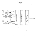
- a specific embodiment of the invention comprises an array of antennae, each with its own wide band receiver or ADC, refer Figs. 2 and 3.
- Fig. 3 differs from Fig. 2 in that Fig. 3 includes channelisation and synthesis functional blocks that assist in paralleling the computation of the processing task.
- One form of channelisation is the division into independent frequency bands. Examples of the implementation of channelising in the frequency domain are the use of poly-phase filter techniques or Fast Fourier transform techniques. Channelising in other domains (e.g. code or spatial) are also possible.
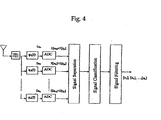
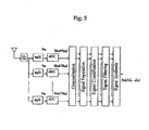
- a further embodiment of the invention comprises the use of a single antenna that provides variable phase delayed versions of the analogue signals it receives into multiple ADCs, refer Figs. 4 and 5.
- Fig. 5 differs from Fig. 4 in that Fig. 5 includes channelisation and synthesis functional blocks that assist in paralleling the computation of the processing task as discussed above.
- the single antenna embodiment is akin to the use of a single receiver element such as a strain gauge or other type of sensor when the invention is applied in a non-RF-based example.
- the ADC elements need not be of particularly high quality (low linearity, etc.) since it is possible having taken this approach, to adequately filter out unwanted frequencies even those generated by the non-linearity of the ADCs.
- the following functionality can be achieved by digital signal processing. Receiver architectures of this type have a number of important potentially advantageous features.
- a number of possible architectures for an RF receiver can be considered, most of them based on:
- FIG.1 A functional architecture of an embodiment of an RF receiving system is depicted in Fig.1.
- An array of N antennae with respective band pass filters and ADCs (10) feeds received signals and added spurious signals into a frequency channelisation device (12) which divides each of the N input streams into M (M may be 1 or more) predetermined bandwidth streams for distribution.
- M may be 1 or more
- an FFT (14) is used to detect signals of interest, to determine where intermodulation products are likely to exist and to provide coarse data for the spatial processing used in the signal separation sub-systems.
- An alternative RF receiver architecture to detect signals of interest could occur as part of the signal separation process.
- the second path (16) includes the detection of co-channel: signals using algorithms such as Eigenvalue Decomposition. If these co-channel signals are spatially distinct they are separated using spatial processing algorithms such as, MUSIC and generalized side lobe cancellation and if they are spatially indistinct they are separated by Higher Order Statistical (HOS) processing algorithms such as Joint Approximate Diagonalization of Eigen-matrices (JADE). Signal classification techniques are then used to identify spurious signals, which are then removed. These processes linearise the output of the ADCs.
- algorithms such as Eigenvalue Decomposition.
- the final stage in the process is the demodulation and decoding (18) of the signals of interest.
- Controlling the total system will be a control and recording system (20), that is typically accessed by a pool of users (22) each of whom are interested in a particular SOI at any one time.
- the invention is adapted to the RF receiver arrangement, but its primary architecture is evident in the array of ADCs, separated either spatially or with filters having a variable phase delay which in such a configuration can provide a higher dynamic range Analogue to Digital conversion than previously achievable.
- the receiver front end has N (32) Analogue to Digital Converters each operating at 80MHz.
- N 32) Analogue to Digital Converters each operating at 80MHz.
- variable and nonuniform sampling may be more appropriate and will give greater bandwidth for the same input and output conditions and allows spurious signals to be more readily identified and thus allows for greater rejection of those signals.
- a non-linear correction system In order to provide the best linearity from each channel it is possible for a non-linear correction system to be used on each channel that is similar to those based on work by Tsimbinos and Lever in the IEEE International Conference on Acoustics, Speech and Signal Processing, April 1994.
- a further way to channelize is to sub-sample all the individual ADC rates or reduce their sampling rates. Provided that the total sample rate exceeds Nyquist, it is possible to use the spatial information to unambiguously identify and separate all the signals. In the spatial example it is a preferred embodiment that the separation would be done by Ricatti number theory.
- the signal detection path used to detect signals of interest, to determine where intermodulation products are likely to exist and to provide coarse data for the spatial processing used in the signal separation sub-systems.
- 32 channels of 10MHz data will undergo a Fourier analysis and then subsequent processing to look for signals of interest.
- the Fourier transforms there is a second level of processing to combine the 32 channels spatially and to look for new signals. This leads to a processing demand similar to that of the FFT, and as such, it would be reasonable to allocate approximately 60Gflops to this subsystem.
- Fig. 1 there is a signal separation and detection path, and there will need to be a separate system for each user. In the case of a preferable H.F. communications installation there are likely to be about 20 operator positions.
- each of the 32 channels is first reduced to a 10KHz bandwidth using digital filtering techniques.
- a preferred example is a Digital Down Converter (DDC) and a dual rate filter.
- DDC Digital Down Converter
- the first filter will be a fast, but short FIR (say of the order 10 at the 10MHz data rate - say about a 20Mflops processing power requirement).
- the 'narrow band receivers' After decimation (to, say a 1MHz rate) there is a second longer filter (at the 1MHz rate of order 100 - say about a 20Mflops processing power requirement) followed by decimation to the final 10kHz bandwidth.
- the final stage in the process is the demodulation and decoding of the signal of interest, but given that this occurs with a single 10kHz data stream it is likely to be less than 5Mflops and as such can be neglected in this calculation.
- ADC performance has been improving at a rate of about 1.5 bits every 6-8 years, and there became available an ADC with 14 bit linearity at 100Msamples/second on the market in the year 2000. This is not, by itself adequate for a single channel H.F. receiver but it does offer a linearity of about 80dB in the normal two-tone tests in which dynamic range is governed by the SFDR.
- optical ADCs which may result in an improvement in performance (e.g. greater than 100dB SFDR with greater than 100MHz bandwidth), and further research into non-linear compensation techniques will improve the linearity of existing ADCs. Furthermore, there are programs to improve the dynamic range of ADCs.
- a significant factor when considering the use of ADCs is that there will be spurious signals generated by them, commonly referred to as "birdies" especially from the larger received signals.
- birdies are spurious signals generated by them, commonly referred to as "birdies" especially from the larger received signals.
- the inventors have realized that this is not necessarily a disadvantage. Since these birdies have an apparent spatial origin, known co-channel techniques can be used to remove them in a similar way to other signals of interest.
- Co-channel separation algorithms are known in the art. The most common techniques are known for their ability to separate signals and can be found in texts such at Tsui, James Bao-yen, "Digital Microwave Receivers", 1989 Artec House, Inc.
- a typical intermodulation product would be the 3 rd order product created by two large signals. Its "true frequency” would be at 2*F1+F2 and the resulting intermodulation product would have a phase difference between elements on the antenna array of 2* ⁇ 1 + ⁇ 2 . However if the "true frequency" is above the Nyquist frequency of the system ( i.e. >1 ⁇ 2 the sampling rate) it will be aliased to some apparent frequency less than Nyquist. Similarly, the measured phase angle in a real system can only be between ⁇ . These two phenomena have the overall results of randomizing the frequency and phase of all intermodulation products over the range 0 to F max and from ⁇ respectively.
- a two-dimensional array will allow a simple filter to remove 1- ⁇ /12, or about 74% of all intermodulation products generated by the ADCs.
- a three-dimensional array would permit 1- ⁇ /24 or about 87% of all intermodulation products to be removed since they do not come from physically realizable space - i.e. they are "ghosts".
- this embodiment using digital array architecture is in the H.F. band.
- the 87% "de-ghosting" level is seen as an upper limit that may be achievable with advanced antenna array architectures whilst the 74% de-ghosting is a lower level that can be achieved readily with a simple two-dimensional, or crossed array.
- HOS High Order Statistical
- the statistical difference is mainly brought about by the process by which an intermodulation product is formed.
- one of the large intermodulation products is the third harmonic of a signal ( i . e . 3F), and if the original SOI were a BFSK signal with two tones separated by 1kHz the resulting third harmonic would have 3kHz separations and hence different statistics.
- the best metric is not the SFDR of the system, but rather the probability of detecting and being able to demodulate a signal at a given power level in a specific Frazel cell.
- the operating dynamic range can be much greater than the SFDR of the system and for the purposes of this specification, it is assumed that the "effective SFDR" of the receiver is a sensible metric for comparison purposes between digital and non-digital systems.
- the best ADCs are achieving aperture jitters which approach 05 picoseconds as was shown in the study Walden "ADC Survey and Analysis” IEEE SAC vol 14, #4 at Fig. 5.
- the best ADC currently available with a 75MHz-sampling rate offers an SFDR of almost 14 bits (i.e. 84dB).
- Tflops/Tops Tera-flops/Tera-ops region
Landscapes
- Engineering & Computer Science (AREA)
- Theoretical Computer Science (AREA)
- Noise Elimination (AREA)
- Radar Systems Or Details Thereof (AREA)
- Devices For Indicating Variable Information By Combining Individual Elements (AREA)
- Electrochromic Elements, Electrophoresis, Or Variable Reflection Or Absorption Elements (AREA)
- Compression, Expansion, Code Conversion, And Decoders (AREA)
- Circuits Of Receivers In General (AREA)
- Error Detection And Correction (AREA)
Claims (8)
- Analog-Digital-Wandler-Vorrichtung zum Wandeln eines oder mehrerer analogen Signale, die an einem Empfängerelement eintreffen, das ein empfangenes Ausgabesignal zur Verfügung stellt, wobei die Vorrichtung gekennzeichnet ist durch:ein oder mehrere variable Phasenlaufzeitmittel zum Erzeugen einer Mehrzahl von phasenverzögerten Versionen des empfangenen Ausgabesignals;ein oder mehrere entsprechende Analog-Digital-Wandler (ADC) für das oder jedes der variablen Phasenlaufzeitmittel, wobei das Empfängerelement, das/die variablen Phasenlaufzeitmittel und alle ADC nicht-lineare Effekte in den analogen und/oder digitalen Prozessen des Empfangens, Verzögerns und/oder Wandelns analoger Signale und des Erzeugens entsprechender ADC-Ausgangssignale, die die digitalen Entsprechungen des einen oder der mehreren Signale zuzüglich der sich aus den nicht-linearen Effekten ergebenden Störsignale darstellen, aufweisen; Aufbereitungsmittel zum Identifizieren der Störsignale durch:(a) Analyse der Phasenbeziehungen der ADC-Ausgangssignale gemäß den durch die variablen Phasenlaufzeitmittel eingefügten Phasenverzögerungen; und/oder(b) statistische Analyse höherer Ordnung der ADC-Ausgangssignale; und Filtermittel zum Entfernen von identifizierten Störsignalen.
- Analog-Digital-Wandler-Vorrichtung nach Anspruch 1, wobei die Analyse der Phasenbeziehungen und die statistische Analyse höherer Ordnung parallel zueinander oder hintereinander ausgeführt werden.
- Analog-Digital-Wandler-Vorrichtung nach Anspruch 2, weiterhin umfassend Kanalisiermittel zum Aufteilen der ADC-Ausgangssignale in multiple Kanäle vor der Aufbereitung und Filterung.
- Analog-Digital-Wandler-Vorrichtung nach Anspruch 3, weiterhin umfassend ein Synthesemittel zum Wiederherstellen zweier oder mehrerer der multiplen Kanäle in eine aufbereitete und gefilterte digitale Entsprechung des einen analogen Signals bzw. der mehreren analogen Signale.
- Verfahren zum Identifizieren und Herausfiltern von Störsignalen aus den digitalen Entsprechungen eines oder mehrerer Signale, beinhaltend folgende Schritte:(a) Empfangen eines oder mehrerer analoger Signale in einem Empfängerelement, wodurch ein Empfängerausgangssignal zur Verfügung gestellt wird, wobei das Empfängerelement als Folge der nicht-linearen Eigenschaften des analogen Prozesses des Empfangens des einen oder der mehreren Signale Störsignale beisteuert;(b) Empfangen des Empfängerausgangssignals an einem oder mehreren variablen Phasenlaufzeitmitteln und Erzeugen einer Mehrzahl von phasenverzögerten Versionen des Ausgangssignals, wobei die variablen Phasenlaufzeitmittel als Folge der nicht-linearen Eigenschaften des analogen Prozesses des Erzeugens der phasenverzögerten Versionen Störsignale beisteuern;(c) Zurverfügungstellen eines Analog-Digital-Wandlers (ADC) für jedes der variablen Phasenlaufzeitmittel, wobei jeder ADC als Folge der nicht-linearen Eigenschaften der von dem ADC ausgeführten analogen und digitalen Prozesses zum Umwandeln des Ausgangssignals eines jeweiligen Phasenlaufzeitmittels in eine digitale Entsprechung Störsignale beisteuert, wobei das Verfahren gekennzeichnet ist durch:(d) Aufbereiten der digitalen Entsprechungen zum Identifizieren der Störsignale durch(i) Analysieren der Phasenbeziehungen der ADC-Ausgangssignale gemäß den durch die variablen Phasenlaufzeitmittel eingefügten Phasenverzögerungen; und/oder(ii) statistische Analyse höherer Ordnung der ADC-Ausgangssignale; und(e) Filtern zum Entfernen der identifizierten Störsignale.
- Verfahren nach Anspruch 5, wobei die Analyse der Phasenbeziehungen und die statistische Analyse höherer Ordnung parallel zueinander oder hintereinander ausgeführt werden.
- Verfahren nach Anspruch 5 oder 6, wobei das Erzeugen der digitalen Entsprechungen in Schritt (c) das Unterteilen der digitalen Entsprechungen in multiple Kanäle beinhaltet.
- Verfahren nach Anspruch 7, weiterhin umfassend den Schritt: (f) Synthetisieren der durch den Schritt des Filterns (e) rehaltenen digitalen Entsprechungen zum Wiederherstellen zweier oder mehrerer der multiplen Kanäle in eine aufbereitete und gefilterte digitale Entsprechung des einen analogen Signals bzw. der mehreren analogen Signale.
Applications Claiming Priority (3)
| Application Number | Priority Date | Filing Date | Title |
|---|---|---|---|
| AUPQ3814A AUPQ381499A0 (en) | 1999-11-02 | 1999-11-02 | Enhanced direct digitising array arrangement |
| AUPQ381499 | 1999-11-02 | ||
| EP00972473A EP1228568B1 (de) | 1999-11-02 | 2000-11-02 | Verbesserte vorrichtung zur direkten digitalisiermatrix |
Related Parent Applications (1)
| Application Number | Title | Priority Date | Filing Date |
|---|---|---|---|
| EP00972473A Division EP1228568B1 (de) | 1999-11-02 | 2000-11-02 | Verbesserte vorrichtung zur direkten digitalisiermatrix |
Publications (2)
| Publication Number | Publication Date |
|---|---|
| EP1580894A1 EP1580894A1 (de) | 2005-09-28 |
| EP1580894B1 true EP1580894B1 (de) | 2007-01-24 |
Family
ID=3817962
Family Applications (2)
| Application Number | Title | Priority Date | Filing Date |
|---|---|---|---|
| EP00972473A Expired - Lifetime EP1228568B1 (de) | 1999-11-02 | 2000-11-02 | Verbesserte vorrichtung zur direkten digitalisiermatrix |
| EP05075997A Expired - Lifetime EP1580894B1 (de) | 1999-11-02 | 2000-11-02 | Verbesserte Vorrichtung zur direkten Digitalisiermatrix |
Family Applications Before (1)
| Application Number | Title | Priority Date | Filing Date |
|---|---|---|---|
| EP00972473A Expired - Lifetime EP1228568B1 (de) | 1999-11-02 | 2000-11-02 | Verbesserte vorrichtung zur direkten digitalisiermatrix |
Country Status (7)
| Country | Link |
|---|---|
| US (1) | US6894630B1 (de) |
| EP (2) | EP1228568B1 (de) |
| AT (2) | ATE352904T1 (de) |
| AU (1) | AUPQ381499A0 (de) |
| CA (1) | CA2389976A1 (de) |
| DE (2) | DE60033205T2 (de) |
| WO (1) | WO2001033717A1 (de) |
Families Citing this family (11)
| Publication number | Priority date | Publication date | Assignee | Title |
|---|---|---|---|---|
| US7336729B2 (en) * | 2001-03-01 | 2008-02-26 | Broadcom Corporation | Digital signal processing based de-serializer |
| JP3947185B2 (ja) * | 2004-06-01 | 2007-07-18 | 株式会社アドバンテスト | アナログディジタル変換方法、及びアナログディジタル変換装置 |
| US8185077B2 (en) * | 2009-01-20 | 2012-05-22 | Raytheon Company | Method and system for noise suppression in antenna |
| US8433001B2 (en) * | 2009-09-30 | 2013-04-30 | Motorola Solutions, Inc. | Method and apparatus for mitigation of interference |
| US8477892B2 (en) * | 2009-09-30 | 2013-07-02 | Motorola Solutions, Inc. | Method and apparatus for mitigation of interference |
| US8508395B2 (en) * | 2010-07-19 | 2013-08-13 | Massachusetts Institute Of Technology | Time varying quantization-based linearity enhancement of signal converters and mixed-signal systems |
| US9998158B2 (en) | 2015-05-27 | 2018-06-12 | Finesse Wireless, Inc. | Cancellation of spurious intermodulation products produced in nonlinear channels by frequency hopped signals and spurious signals |
| US11489847B1 (en) * | 2018-02-14 | 2022-11-01 | Nokomis, Inc. | System and method for physically detecting, identifying, and diagnosing medical electronic devices connectable to a network |
| US11677410B2 (en) * | 2019-01-18 | 2023-06-13 | Precision Receivers Incorporated | Spur reduction for analog-to-digital converters |
| WO2020236209A1 (en) * | 2019-05-22 | 2020-11-26 | Adesto Technologies Corporation | Pulse width signal overlap compensation techniques |
| KR20250086643A (ko) * | 2022-09-16 | 2025-06-13 | 에이텐 시스템즈 인코포레이티드 디/비/에이 에어라나큘러스 | 딥 러닝을 사용한 동일채널 신호 분류 |
Family Cites Families (13)
| Publication number | Priority date | Publication date | Assignee | Title |
|---|---|---|---|---|
| US4675606A (en) | 1985-07-29 | 1987-06-23 | Suman Ganguly | Magnetometers for detecting metallic objects in earth's magnetic field |
| GB8912780D0 (en) * | 1989-06-02 | 1989-07-19 | Gen Electric Co Plc | Analogue to digital converters |
| US5021792A (en) * | 1990-01-12 | 1991-06-04 | Rockwell International Corporation | System for determining direction or attitude using GPS satellite signals |
| GB9109637D0 (en) | 1991-05-03 | 1991-06-26 | Marconi Gec Ltd | Analogue-to-digital and digital-to-analogue converters |
| EP0579838B1 (de) * | 1992-01-08 | 1998-09-09 | Ikegami Tsushinki Co., Ltd. | Festkörperbildaufnahmevorrichtung und -element hierfür |
| US5262789A (en) * | 1992-04-30 | 1993-11-16 | General Electric Company | Source identification system for closely separated spatial sources |
| US5294926A (en) * | 1992-10-09 | 1994-03-15 | Hewlett-Packard Company | Timing and amplitude error estimation for time-interleaved analog-to-digital converters |
| US5568142A (en) * | 1994-10-20 | 1996-10-22 | Massachusetts Institute Of Technology | Hybrid filter bank analog/digital converter |
| DE19581533C2 (de) | 1994-12-29 | 1999-02-25 | Motorola Inc | Verfahren zum Digitalisieren eines Breitbandfrequenzsignals und zugehöriger Breitbandfrequenzsignaldigitalisierer |
| US5748683A (en) * | 1994-12-29 | 1998-05-05 | Motorola, Inc. | Multi-channel transceiver having an adaptive antenna array and method |
| JP3498088B2 (ja) * | 1995-05-31 | 2004-02-16 | 株式会社ルネサステクノロジ | 集積回路 |
| US5815117A (en) * | 1997-01-02 | 1998-09-29 | Raytheon Company | Digital direction finding receiver |
| US6463093B1 (en) * | 1998-07-30 | 2002-10-08 | Airnet Communications Corporation | Method and apparatus to reduce spurious and intermodulation products in wireless broadband multi-carrier digital transceiver equipment through static non-linearity correction of digital conversion components |
-
1999
- 1999-11-02 AU AUPQ3814A patent/AUPQ381499A0/en not_active Abandoned
-
2000
- 2000-11-02 AT AT05075997T patent/ATE352904T1/de not_active IP Right Cessation
- 2000-11-02 AT AT00972473T patent/ATE388524T1/de not_active IP Right Cessation
- 2000-11-02 DE DE60033205T patent/DE60033205T2/de not_active Expired - Lifetime
- 2000-11-02 WO PCT/AU2000/001345 patent/WO2001033717A1/en not_active Ceased
- 2000-11-02 EP EP00972473A patent/EP1228568B1/de not_active Expired - Lifetime
- 2000-11-02 DE DE60038245T patent/DE60038245T2/de not_active Expired - Lifetime
- 2000-11-02 CA CA002389976A patent/CA2389976A1/en not_active Abandoned
- 2000-11-02 EP EP05075997A patent/EP1580894B1/de not_active Expired - Lifetime
- 2000-11-02 US US10/129,286 patent/US6894630B1/en not_active Expired - Fee Related
Also Published As
| Publication number | Publication date |
|---|---|
| US6894630B1 (en) | 2005-05-17 |
| CA2389976A1 (en) | 2001-05-10 |
| DE60038245D1 (de) | 2008-04-17 |
| ATE388524T1 (de) | 2008-03-15 |
| DE60033205D1 (de) | 2007-03-15 |
| ATE352904T1 (de) | 2007-02-15 |
| EP1580894A1 (de) | 2005-09-28 |
| EP1228568A4 (de) | 2003-03-26 |
| EP1228568A1 (de) | 2002-08-07 |
| DE60033205T2 (de) | 2007-12-20 |
| DE60038245T2 (de) | 2009-03-12 |
| EP1228568B1 (de) | 2008-03-05 |
| WO2001033717A1 (en) | 2001-05-10 |
| AUPQ381499A0 (en) | 1999-11-25 |
Similar Documents
| Publication | Publication Date | Title |
|---|---|---|
| US20180083816A1 (en) | Methods and apparatus for array-based compressed sensing | |
| US8582694B2 (en) | Adaptive digital receiver | |
| EP1580894B1 (de) | Verbesserte Vorrichtung zur direkten Digitalisiermatrix | |
| US9374111B2 (en) | Multi-stage charge re-use analog circuits | |
| EP2537255B1 (de) | Vorrichtung und verfahren zur umwandlung eines analog-zeitbereichssignals in ein digitalfrequenzbereichssignal sowie vorrichtung und verfahren zur umwandlung eines analogzeitbereichssignals in ein digitalzeitbereichssignal | |
| JP2008501289A (ja) | デジタイザ構成 | |
| US20100039098A1 (en) | System for extraction and analysis of significant radioelectric signals | |
| US20120075129A1 (en) | Calibration of impairments in a multichannel time-interleaved adc | |
| CN102445679A (zh) | 三信道空间谱估计测向系统的测向方法 | |
| WO2012118543A2 (en) | Method and apparatus for complex in-phase quadrature polyphase nonlinear equalization | |
| US8837956B1 (en) | Pipelined receiver system and method | |
| US8401134B1 (en) | Broadband high dynamic range digital receiving system for electromagnetic signals | |
| Tietche et al. | FPGA-based simultaneous multichannel FM broadcast receiver for audio indexing applications in consumer electronics scenarios | |
| AU773665B2 (en) | Enhanced direct digitising array arrangement | |
| Huang et al. | General analysis of resolution enhancement on time-synchronized sampling and its multi-resolution solution in 20GSPS acquisition system | |
| Khakpour et al. | Adaptive noise cancellation based architecture for correction of gain and offset mismatch errors in time-interleaved ADC | |
| Nawaz et al. | Comparative survey on time interleaved analog to digital converter mismatches compensation techniques | |
| Luo et al. | A novel fast and wide range background timing mismatch calibration algorithm for TIADCs | |
| Konuk et al. | Calibration and equalization methods for mismatch errors in a high frequency two-channel time-interleaved ADC | |
| US20220113373A1 (en) | Systems and methods for processing errors in digital beamforming receivers | |
| CN120729309A (zh) | 一种基于非变频频率交织的宽带采样系统及方法 | |
| El-Sankary et al. | New sampling method to improve the SFDR of wide bandwidth ADC dedicated to next generation wireless transceiver | |
| CN120710503A (zh) | 基于通道组合的ti-adc时序失配校准系统 | |
| CN118971930A (zh) | 一种高性能一体化信号接收方法及装置 | |
| Sallam et al. | Aperture distribution reconstruction of phased array antenna with single RF channel based on non-uniform spatial sampling of array elements |
Legal Events
| Date | Code | Title | Description |
|---|---|---|---|
| PUAI | Public reference made under article 153(3) epc to a published international application that has entered the european phase |
Free format text: ORIGINAL CODE: 0009012 |
|
| 17P | Request for examination filed |
Effective date: 20050427 |
|
| AC | Divisional application: reference to earlier application |
Ref document number: 1228568 Country of ref document: EP Kind code of ref document: P |
|
| AK | Designated contracting states |
Kind code of ref document: A1 Designated state(s): AT BE CH CY DE DK ES FI FR GB GR IE IT LI LU MC NL PT SE TR |
|
| AKX | Designation fees paid |
Designated state(s): AT BE CH CY DE DK ES FI FR GB GR IE IT LI LU MC NL PT SE TR |
|
| GRAP | Despatch of communication of intention to grant a patent |
Free format text: ORIGINAL CODE: EPIDOSNIGR1 |
|
| GRAS | Grant fee paid |
Free format text: ORIGINAL CODE: EPIDOSNIGR3 |
|
| GRAA | (expected) grant |
Free format text: ORIGINAL CODE: 0009210 |
|
| AC | Divisional application: reference to earlier application |
Ref document number: 1228568 Country of ref document: EP Kind code of ref document: P |
|
| AK | Designated contracting states |
Kind code of ref document: B1 Designated state(s): AT BE CH CY DE DK ES FI FR GB GR IE IT LI LU MC NL PT SE TR |
|
| PG25 | Lapsed in a contracting state [announced via postgrant information from national office to epo] |
Ref country code: NL Free format text: LAPSE BECAUSE OF FAILURE TO SUBMIT A TRANSLATION OF THE DESCRIPTION OR TO PAY THE FEE WITHIN THE PRESCRIBED TIME-LIMIT Effective date: 20070124 Ref country code: CH Free format text: LAPSE BECAUSE OF FAILURE TO SUBMIT A TRANSLATION OF THE DESCRIPTION OR TO PAY THE FEE WITHIN THE PRESCRIBED TIME-LIMIT Effective date: 20070124 Ref country code: DK Free format text: LAPSE BECAUSE OF FAILURE TO SUBMIT A TRANSLATION OF THE DESCRIPTION OR TO PAY THE FEE WITHIN THE PRESCRIBED TIME-LIMIT Effective date: 20070124 Ref country code: LI Free format text: LAPSE BECAUSE OF FAILURE TO SUBMIT A TRANSLATION OF THE DESCRIPTION OR TO PAY THE FEE WITHIN THE PRESCRIBED TIME-LIMIT Effective date: 20070124 Ref country code: AT Free format text: LAPSE BECAUSE OF FAILURE TO SUBMIT A TRANSLATION OF THE DESCRIPTION OR TO PAY THE FEE WITHIN THE PRESCRIBED TIME-LIMIT Effective date: 20070124 |
|
| REG | Reference to a national code |
Ref country code: GB Ref legal event code: FG4D |
|
| REG | Reference to a national code |
Ref country code: CH Ref legal event code: EP |
|
| REG | Reference to a national code |
Ref country code: IE Ref legal event code: FG4D |
|
| REF | Corresponds to: |
Ref document number: 60033205 Country of ref document: DE Date of ref document: 20070315 Kind code of ref document: P |
|
| PG25 | Lapsed in a contracting state [announced via postgrant information from national office to epo] |
Ref country code: SE Free format text: LAPSE BECAUSE OF FAILURE TO SUBMIT A TRANSLATION OF THE DESCRIPTION OR TO PAY THE FEE WITHIN THE PRESCRIBED TIME-LIMIT Effective date: 20070424 |
|
| PG25 | Lapsed in a contracting state [announced via postgrant information from national office to epo] |
Ref country code: ES Free format text: LAPSE BECAUSE OF FAILURE TO SUBMIT A TRANSLATION OF THE DESCRIPTION OR TO PAY THE FEE WITHIN THE PRESCRIBED TIME-LIMIT Effective date: 20070505 |
|
| PG25 | Lapsed in a contracting state [announced via postgrant information from national office to epo] |
Ref country code: PT Free format text: LAPSE BECAUSE OF FAILURE TO SUBMIT A TRANSLATION OF THE DESCRIPTION OR TO PAY THE FEE WITHIN THE PRESCRIBED TIME-LIMIT Effective date: 20070625 |
|
| REG | Reference to a national code |
Ref country code: CH Ref legal event code: PL |
|
| NLV1 | Nl: lapsed or annulled due to failure to fulfill the requirements of art. 29p and 29m of the patents act | ||
| ET | Fr: translation filed | ||
| PLBE | No opposition filed within time limit |
Free format text: ORIGINAL CODE: 0009261 |
|
| STAA | Information on the status of an ep patent application or granted ep patent |
Free format text: STATUS: NO OPPOSITION FILED WITHIN TIME LIMIT |
|
| 26N | No opposition filed |
Effective date: 20071025 |
|
| PG25 | Lapsed in a contracting state [announced via postgrant information from national office to epo] |
Ref country code: BE Free format text: LAPSE BECAUSE OF FAILURE TO SUBMIT A TRANSLATION OF THE DESCRIPTION OR TO PAY THE FEE WITHIN THE PRESCRIBED TIME-LIMIT Effective date: 20070124 |
|
| PG25 | Lapsed in a contracting state [announced via postgrant information from national office to epo] |
Ref country code: GR Free format text: LAPSE BECAUSE OF FAILURE TO SUBMIT A TRANSLATION OF THE DESCRIPTION OR TO PAY THE FEE WITHIN THE PRESCRIBED TIME-LIMIT Effective date: 20070425 Ref country code: IT Free format text: LAPSE BECAUSE OF FAILURE TO SUBMIT A TRANSLATION OF THE DESCRIPTION OR TO PAY THE FEE WITHIN THE PRESCRIBED TIME-LIMIT Effective date: 20070124 |
|
| PG25 | Lapsed in a contracting state [announced via postgrant information from national office to epo] |
Ref country code: MC Free format text: LAPSE BECAUSE OF NON-PAYMENT OF DUE FEES Effective date: 20071130 |
|
| PG25 | Lapsed in a contracting state [announced via postgrant information from national office to epo] |
Ref country code: IE Free format text: LAPSE BECAUSE OF NON-PAYMENT OF DUE FEES Effective date: 20071102 |
|
| PG25 | Lapsed in a contracting state [announced via postgrant information from national office to epo] |
Ref country code: CY Free format text: LAPSE BECAUSE OF FAILURE TO SUBMIT A TRANSLATION OF THE DESCRIPTION OR TO PAY THE FEE WITHIN THE PRESCRIBED TIME-LIMIT Effective date: 20070124 |
|
| PG25 | Lapsed in a contracting state [announced via postgrant information from national office to epo] |
Ref country code: FI Free format text: LAPSE BECAUSE OF FAILURE TO SUBMIT A TRANSLATION OF THE DESCRIPTION OR TO PAY THE FEE WITHIN THE PRESCRIBED TIME-LIMIT Effective date: 20070124 Ref country code: LU Free format text: LAPSE BECAUSE OF NON-PAYMENT OF DUE FEES Effective date: 20071102 |
|
| PG25 | Lapsed in a contracting state [announced via postgrant information from national office to epo] |
Ref country code: TR Free format text: LAPSE BECAUSE OF FAILURE TO SUBMIT A TRANSLATION OF THE DESCRIPTION OR TO PAY THE FEE WITHIN THE PRESCRIBED TIME-LIMIT Effective date: 20070124 |
|
| PGFP | Annual fee paid to national office [announced via postgrant information from national office to epo] |
Ref country code: FR Payment date: 20101130 Year of fee payment: 11 |
|
| PGFP | Annual fee paid to national office [announced via postgrant information from national office to epo] |
Ref country code: DE Payment date: 20101119 Year of fee payment: 11 |
|
| PGFP | Annual fee paid to national office [announced via postgrant information from national office to epo] |
Ref country code: GB Payment date: 20101105 Year of fee payment: 11 |
|
| GBPC | Gb: european patent ceased through non-payment of renewal fee |
Effective date: 20111102 |
|
| REG | Reference to a national code |
Ref country code: FR Ref legal event code: ST Effective date: 20120731 |
|
| REG | Reference to a national code |
Ref country code: DE Ref legal event code: R119 Ref document number: 60033205 Country of ref document: DE Effective date: 20120601 |
|
| PG25 | Lapsed in a contracting state [announced via postgrant information from national office to epo] |
Ref country code: GB Free format text: LAPSE BECAUSE OF NON-PAYMENT OF DUE FEES Effective date: 20111102 |
|
| PG25 | Lapsed in a contracting state [announced via postgrant information from national office to epo] |
Ref country code: FR Free format text: LAPSE BECAUSE OF NON-PAYMENT OF DUE FEES Effective date: 20111130 |
|
| PG25 | Lapsed in a contracting state [announced via postgrant information from national office to epo] |
Ref country code: DE Free format text: LAPSE BECAUSE OF NON-PAYMENT OF DUE FEES Effective date: 20120601 |