EP3982479B1 - Metamaterial adjustable capacitor structure - Google Patents
Metamaterial adjustable capacitor structure Download PDFInfo
- Publication number
- EP3982479B1 EP3982479B1 EP20735471.3A EP20735471A EP3982479B1 EP 3982479 B1 EP3982479 B1 EP 3982479B1 EP 20735471 A EP20735471 A EP 20735471A EP 3982479 B1 EP3982479 B1 EP 3982479B1
- Authority
- EP
- European Patent Office
- Prior art keywords
- metamaterial
- capacitor structure
- variable capacitor
- structure according
- based variable
- Prior art date
- Legal status (The legal status is an assumption and is not a legal conclusion. Google has not performed a legal analysis and makes no representation as to the accuracy of the status listed.)
- Active
Links
Images


Classifications
-
- H—ELECTRICITY
- H01—ELECTRIC ELEMENTS
- H01P—WAVEGUIDES; RESONATORS, LINES, OR OTHER DEVICES OF THE WAVEGUIDE TYPE
- H01P1/00—Auxiliary devices
- H01P1/18—Phase-shifters
- H01P1/181—Phase-shifters using ferroelectric devices
-
- H—ELECTRICITY
- H01—ELECTRIC ELEMENTS
- H01G—CAPACITORS; CAPACITORS, RECTIFIERS, DETECTORS, SWITCHING DEVICES, LIGHT-SENSITIVE OR TEMPERATURE-SENSITIVE DEVICES OF THE ELECTROLYTIC TYPE
- H01G7/00—Capacitors in which the capacitance is varied by non-mechanical means; Processes of their manufacture
- H01G7/06—Capacitors in which the capacitance is varied by non-mechanical means; Processes of their manufacture having a dielectric selected for the variation of its permittivity with applied voltage, i.e. ferroelectric capacitors
-
- H—ELECTRICITY
- H01—ELECTRIC ELEMENTS
- H01P—WAVEGUIDES; RESONATORS, LINES, OR OTHER DEVICES OF THE WAVEGUIDE TYPE
- H01P1/00—Auxiliary devices
- H01P1/18—Phase-shifters
-
- H—ELECTRICITY
- H01—ELECTRIC ELEMENTS
- H01P—WAVEGUIDES; RESONATORS, LINES, OR OTHER DEVICES OF THE WAVEGUIDE TYPE
- H01P1/00—Auxiliary devices
- H01P1/18—Phase-shifters
- H01P1/184—Strip line phase-shifters
-
- H—ELECTRICITY
- H01—ELECTRIC ELEMENTS
- H01P—WAVEGUIDES; RESONATORS, LINES, OR OTHER DEVICES OF THE WAVEGUIDE TYPE
- H01P5/00—Coupling devices of the waveguide type
- H01P5/02—Coupling devices of the waveguide type with invariable factor of coupling
- H01P5/022—Transitions between lines of the same kind and shape, but with different dimensions
- H01P5/028—Transitions between lines of the same kind and shape, but with different dimensions between strip lines
-
- H—ELECTRICITY
- H01—ELECTRIC ELEMENTS
- H01Q—ANTENNAS, i.e. RADIO AERIALS
- H01Q3/00—Arrangements for changing or varying the orientation or the shape of the directional pattern of the waves radiated from an antenna or antenna system
- H01Q3/26—Arrangements for changing or varying the orientation or the shape of the directional pattern of the waves radiated from an antenna or antenna system varying the relative phase or relative amplitude of energisation between two or more active radiating elements; varying the distribution of energy across a radiating aperture
- H01Q3/30—Arrangements for changing or varying the orientation or the shape of the directional pattern of the waves radiated from an antenna or antenna system varying the relative phase or relative amplitude of energisation between two or more active radiating elements; varying the distribution of energy across a radiating aperture varying the relative phase between the radiating elements of an array
- H01Q3/34—Arrangements for changing or varying the orientation or the shape of the directional pattern of the waves radiated from an antenna or antenna system varying the relative phase or relative amplitude of energisation between two or more active radiating elements; varying the distribution of energy across a radiating aperture varying the relative phase between the radiating elements of an array by electrical means
- H01Q3/36—Arrangements for changing or varying the orientation or the shape of the directional pattern of the waves radiated from an antenna or antenna system varying the relative phase or relative amplitude of energisation between two or more active radiating elements; varying the distribution of energy across a radiating aperture varying the relative phase between the radiating elements of an array by electrical means with variable phase-shifters
Definitions
- the present invention relates to the field of phase shifter and antenna technology, particularly to the continually analog metamaterial-based variable capacitor.
- variable capacitor is a capacitor of which its capacitance can be adjusted within a certain range. It is widely used in the time-frequency response, frequency selection, phase shift control, transmission matching and other technology fields, especially the realization method based on the variable capacitor structure of phase shifter became the technical hot spot.
- phase shifters are widely used in many RF devices such as the phased array antennas, phase modulators and harmonic distortion cancelers.
- the higher requirements such as the miniaturization, light weight, miniaturized, light weight, low insertion loss, and good flatness within the entire operating bandwidth, large phase shift range, wide operating bandwidth, good input and output port matching, low power consumption, and lower costs for the performance of phase shifters were also presented.
- variable capacitor phase shifters based on the ferroelectric thin film BST, liquid crystal and other metamaterials have received more and more attention because of their large adjustable range of dielectric constant or high FOM and the huge application prospect in the design research with the development of materials science.
- CN 107 453 013 A relates to a phase shifter based on liquid crystal materials.
- US 2014/266897 A1 relates to an electronically steerable planar phase array antenna.
- CN 208 654 481 U relates to a liquid crystal phase shifter and a liquid crystal antenna.
- the present invention discloses a metamaterial-based variable capacitor structure, the structure effectively reduces the size of the variable capacitance structure and the shunt attenuation of the radio frequency signal by the bias circuit, thereby improving the figure of merit (FOM) of the structure, largely solving the miniaturization, batching, integration and cost reduction problems of radio frequency microwave devices and antenna, and also adding more freedom to the antenna design.
- FOM figure of merit
- the present invention has the following beneficial effects:
- the embodiment of the present invention provides a metamaterial-based variable capacitor structure 101, comprising: the first substrate 102 and the second substrate 103 set oppositely, and the metamaterial dielectric layer 107 located between the first substrate 102 and the second substrate 103, the metal floor layer 104 located between the first substrate 102 and the metamaterial dielectric layer 107, at least two periodically arranged gaps 105 and isolation holes 106 on the metal floor layer 104, the microstrip line 108, bias line 109 and choke branch 110 located between the second substrate 103 and the metamaterial dielectric layer 107, and two feeding terminals 111 and 112 on both ends of microstrip line 108.
- Fig. 2(a), (b) and (c) are respectively the top views of the first substrate 102 lower surface, the second substrate 103 upper surface, and overall body of the metamaterial-based variable capacitor structure according to a specific embodiment 1 of the present invention.
- the periodically arranged gaps 105 are slotted on floor layer 104 directly facing the microstrip line 108 to form the slow-wave transmission structure, so that the transmission route required for phase shift 360° in the metamaterial dielectric layer is shortened, thereby effectively reducing the overall structure size and obtaining better FOM.
- the metamaterial-based variable capacitor structure is composed of the metal floor layer 104, the periodically arranged gaps 105, the metamaterial dielectric layer 107, and the microstrip line 108.
- the metamaterial dielectric layer 107 is composed of one or multiple layers of variable dielectric constant material, and the material can be the liquid crystal, ferroelectric thin film BST, etc.
- the dielectric constant of the metamaterial dielectric layer can be adjusted to change the capacitance value of the metamaterial-based variable capacitor, thereby changing the phase shift amount of the metamaterial-based phase shifter.
- the bias line 109 for changing the dielectric constant of the metamaterial dielectric layer 107 is loaded on the microstrip line 108.
- the isolation hole 106 is punched on the corresponding bias line 109 at the floor layer 104 where the isolation hole is close to the microstrip line 108.
- the principle of radio frequency transmission line mismatch caused by the impedance mutation can effectively suppress the phenomenon of radio frequency signal loss caused by the transmission along the bias line.
- the structure can greatly reduce the shunt attenuation of RF signals by the bias line compared with the conventional bias line.
- the embodiment of the present invention provides a metamaterial-based variable capacitor structure 201, comprising: the first substrate 102 and the second substrate 103 set oppositely, and the metamaterial dielectric layer 107 located between the first substrate 102 and the second substrate 103, the metal floor layer 104 located between the first substrate 102 and the metamaterial dielectric layer 107, at least two periodically arranged gaps 105 and isolation holes 106 on the metal floor layer 104, the microstrip line 108 between the second substrate 103 and the metamaterial dielectric layer 107, the branches 202, the bias line 109 and choke branch 110 periodically loaded on the microstrip line 108, and two feeding terminals 111 and 112 on both ends of microstrip line 108.
- Fig. 4(a) , (b) and (c) are respectively the top views of the first substrate 102 lower surface, the second substrate 103 upper surface, and overall body of the metamaterial-based variable capacitor structure according to a specific embodiment 2 of the present invention.
- the periodically arranged gaps 105 on the floor layer 104 directly facing the microstrip line 108 and the branches 202 periodically loaded on the microstrip line 108 together form the slow-wave transmission structure, so that the transmission route required for phase shift 360° in the metamaterial dielectric layer is shortened, thereby effectively reducing the size of phase shifter and obtaining better FOM.
- the metamaterial-based variable capacitor structure is composed of the metal floor layer 104, the periodically arranged gaps 105, the metamaterial dielectric layer 107, and the microstrip line 108.
- the metamaterial dielectric layer 107 is composed of one or multiple layers of variable dielectric constant material, and the material can be the liquid crystal, ferroelectric thin film BST, etc.
- Fig. 4 (d) is the equivalent circuit model according to a specific embodiment 2 of the present invention
- 501 is the equivalent inductance formed by the gaps 105 and the metal floor layer 104
- 601 is the equivalent capacitance formed by the microstrip line 108 and the metal floor layer 104
- 602 is the equivalent variable capacitance formed by the microstrip line 108 and the loaded branches 202 together with the metal floor layer 104.
- the 602 capacitance value can be changed by adjusting the dielectric constant of the metamaterial dielectric layer, thereby changing the phase shift amount of the metamaterial-based phase shifter.
- the bias line 109 for changing the dielectric constant of the metamaterial dielectric layer 107 is loaded on the microstrip line 108 or branch 202.
- the isolation hole 106 is punched on the corresponding bias line 109 at the floor layer 104 where the isolation hole is close to the microstrip line 108.
- the principle of radio frequency transmission line mismatch caused by the impedance mutation can effectively suppress the phenomenon of radio frequency signal loss caused by the transmission along the bias line.
- the structure can greatly reduce the shunt attenuation of RF signals by the bias line compared with the conventional bias line.
- the embodiment of the present invention provides a metamaterial-based variable capacitor 301.
- the structure is a curved connection structure extended from the metamaterial-based variable capacitor 101 described in Embodiment 1. This structure makes the routing of phase shifter more flexible, and can better adapt to the routing of phase shifter under different space conditions.
- the bias line for the metamaterial-based variable capacitors 101, 201 and 301 said in the embodiments of the present invention can be replaced by the bias line 402 made from ITO (indium tin oxide), NiCr (nickel chromium), or some other material with a resistivity greater than 1 ⁇ 10 5 ⁇ m.
- the bias line 402 When the bias line 402 is made from ITO (indium tin oxide), NiCr (nickel chromium), or some other material with a resistivity greater than 1 ⁇ 10 5 ⁇ m, the bias line structure can be loaded with the isolation hole 106 and choke branch 110 according to Embodiments 1, 2 or 3 or directly loaded without the isolation hole 106 and choke branch 110 on the microstrip line 108.
- the thickness of the bias line 402 can be from 10 ⁇ 200nm, and the choke attenuation can be also decreased by properly controlling the thickness and square resistance of the coating on the bias line 402.
- the choke branch 110 can be either the loaded fan-shaped or the loaded triangular, or but not be limited to the loaded rectangular structure, etc.
Landscapes
- Engineering & Computer Science (AREA)
- Power Engineering (AREA)
- Microelectronics & Electronic Packaging (AREA)
- Waveguide Switches, Polarizers, And Phase Shifters (AREA)
- Semiconductor Integrated Circuits (AREA)
- Waveguide Aerials (AREA)
Description
- The present invention relates to the field of phase shifter and antenna technology, particularly to the continually analog metamaterial-based variable capacitor.
- The variable capacitor is a capacitor of which its capacitance can be adjusted within a certain range. It is widely used in the time-frequency response, frequency selection, phase shift control, transmission matching and other technology fields, especially the realization method based on the variable capacitor structure of phase shifter became the technical hot spot.
- The phase shifters are widely used in many RF devices such as the phased array antennas, phase modulators and harmonic distortion cancelers. In order to obtain better application effect, the higher requirements such as the miniaturization, light weight, miniaturized, light weight, low insertion loss, and good flatness within the entire operating bandwidth, large phase shift range, wide operating bandwidth, good input and output port matching, low power consumption, and lower costs for the performance of phase shifters were also presented.
- There are many realization methods of the existing phase shifters, but they all have certain application limitations. Among them, the active phase shifter consumes large power and has limited application scenarios. In the passive phase shifters, the switch-type phase shifters based on PIN diodes, CMOS, MEMS, etc. can't achieve the continuous phase adjustment, which are limited in the application scenarios that require the miniaturization and high phase shift accuracy; the reflective or variable capacitor phase shifters based on the variable capacitance diodes will reduce the figure of merit (FOM) due to the increased insertion loss in the high-frequency applications and affect performance indicators. In recent years, the variable capacitor phase shifters based on the ferroelectric thin film BST, liquid crystal and other metamaterials have received more and more attention because of their large adjustable range of dielectric constant or high FOM and the huge application prospect in the design research with the development of materials science. There were also many related patent applications, such as electronically steerable plane phased array antenna (
201280058131.4 201810548743.0 201810333111.2 US 20180062266 ), but the existing designs require the longer transmission line to achieve 360° phase shift, thereby resulting in larger size, decreased FOM, etc., which are not conducive to the miniaturization and integration of RF microwave devices and antennas, but also reduce the design freedom of antennas. They are not conducive to the multi-polarization ability of antennas, and increase the design and processing difficulty of the feeding network; In addition, there is no better solution to minimize the influence of the bias circuit for adjusting the dielectric constant of metamaterial dielectric layer on the RF signal.CN 107 453 013 AUS 2014/266897 A1 relates to an electronically steerable planar phase array antenna. AndCN 208 654 481 U relates to a liquid crystal phase shifter and a liquid crystal antenna. - In order to overcome the existing technical deficiencies, the present invention discloses a metamaterial-based variable capacitor structure, the structure effectively reduces the size of the variable capacitance structure and the shunt attenuation of the radio frequency signal by the bias circuit, thereby improving the figure of merit (FOM) of the structure, largely solving the miniaturization, batching, integration and cost reduction problems of radio frequency microwave devices and antenna, and also adding more freedom to the antenna design.
- Technical solution used in the present invention for solving the above-mentioned problems is provided by the claims.
- Compared with the existing technologies, the present invention has the following beneficial effects:
- (1) The present invention fully utilizes the method of slitting the microstrip line floor and loading the branches on the microstrip line to obtain the slow wave effect of the microstrip line, realize the purpose of effectively reducing the phase shifter size and its loss and improve the FOM of phase shifter.
- (2) The present invention utilizes the bias line with isolation holes and choke branches or made from high-resistance ITO (indium tin oxide), NiCr (nickel chromium), or some other material with a resistivity greater than 1×10⁵Ω·m, effectively reducing the adverse effect of the bias circuit on the performance of phase shifter, further improving the FOM of phase shifter; and the bias line with isolation holes and choke branches can be integrated with the transmission line of phase shifter, which reduces the process flow and the production cost compared with existing ITO bias line.
- Various other advantages and benefits will become apparent to those of ordinary skill in the art upon reading the detailed description of the preferred embodiments below. The drawings are only for the purpose of illustrating the preferred embodiments and are not to be considered as limiting the invention. Moreover, the same reference numerals are used throughout the drawings to indicate the same parts. In the drawings:
-
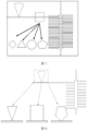
Fig. 1 is the side view of a metamaterial-based capacitor structure according to a specific embodiment 1 of the present invention; -
Fig. 2 (a) is the top view of thefirst substrate 102 lower surface of a metamaterial-based capacitor structure according to a specific embodiment 1 of the present invention; -
Fig. 2 (b) is the top view of thesecond substrate 103 upper surface of a metamaterial-based capacitor structure according to a specific embodiment 1 of the present invention; -
Fig. 2 (c) is the top view of a metamaterial-based capacitor structure according to a specific embodiment 1 of the present invention; -
Fig. 3 is the top view of a metamaterial-based capacitor structure according to a specific embodiment 2 of the present invention; -
Fig. 4 (a) is the top view of the first substrate (102) lower surface of a metamaterial-based capacitor structure according to a specific embodiment 2 of the present invention; -
Fig. 4 (b) is the top view of the second substrate (103) upper surface of a metamaterial-based capacitor structure according to a specific embodiment 2 of the present invention; -
Fig. 4 (c) is the top view of a metamaterial-based capacitor structure according to a specific embodiment 2 of the present invention; -
Fig. 4 (d) is the equivalent circuit model according to a specific embodiment 2 of the present invention; -
Fig. 5 is the top view of a metamaterial-based capacitor structure according to a specific embodiment 3 of the present invention; -
Fig. 6 (a) is the top view of a specific embodiment 1 relating to the bias line made from ITO (indium tin oxide), NiCr (nickel chromium), or some other material with a resistivity greater than 1×10⁵Ω·m; -
Fig. 6 (b) is the top view of a specific embodiment 2 relating to the bias line made from ITO (indium tin oxide), NiCr (nickel chromium), or some other material with a resistivity greater than 1×10⁵Ω·m; -
Fig. 6 (c) is the top view of a specific embodiment 3 relating to the bias line made from ITO (indium tin oxide), NiCr (nickel chromium), or some other material with a resistivity greater than 1×10⁵Ω·m; -
Fig. 7 is the optional shape schematic diagram of theisolation hole 106 on thefloor layer 104 of the present invention; -
Fig. 8 is the optional shape schematic diagram of thechoke branch 110; - Hereinafter, the illustrative embodiments of the present disclosure will be described in more detail with reference to the attached drawings. Although the illustrative embodiments of the present disclosure are shown in the drawings, it should be understood that the present disclosure can be implemented in various forms and should not be limited to the embodiments set forth herein. On the contrary, these embodiments are provided to get a thorough understanding of the present disclosure, and to fully convey the scope of the present disclosure to the technicians in the art.
- As shown in
Fig. 1 , the embodiment of the present invention provides a metamaterial-basedvariable capacitor structure 101, comprising: thefirst substrate 102 and thesecond substrate 103 set oppositely, and the metamaterialdielectric layer 107 located between thefirst substrate 102 and thesecond substrate 103, themetal floor layer 104 located between thefirst substrate 102 and the metamaterialdielectric layer 107, at least two periodically arrangedgaps 105 andisolation holes 106 on themetal floor layer 104, themicrostrip line 108,bias line 109 andchoke branch 110 located between thesecond substrate 103 and the metamaterialdielectric layer 107, and twofeeding terminals microstrip line 108. -
Fig. 2(a), (b) and(c) are respectively the top views of thefirst substrate 102 lower surface, thesecond substrate 103 upper surface, and overall body of the metamaterial-based variable capacitor structure according to a specific embodiment 1 of the present invention. In this structure, the periodically arrangedgaps 105 are slotted onfloor layer 104 directly facing themicrostrip line 108 to form the slow-wave transmission structure, so that the transmission route required for phase shift 360° in the metamaterial dielectric layer is shortened, thereby effectively reducing the overall structure size and obtaining better FOM. - The metamaterial-based variable capacitor structure is composed of the
metal floor layer 104, the periodically arrangedgaps 105, the metamaterialdielectric layer 107, and themicrostrip line 108. Among them, the metamaterialdielectric layer 107 is composed of one or multiple layers of variable dielectric constant material, and the material can be the liquid crystal, ferroelectric thin film BST, etc. The dielectric constant of the metamaterial dielectric layer can be adjusted to change the capacitance value of the metamaterial-based variable capacitor, thereby changing the phase shift amount of the metamaterial-based phase shifter. Thebias line 109 for changing the dielectric constant of the metamaterialdielectric layer 107 is loaded on themicrostrip line 108. In order to reduce the impact of thebias line 109 on the radio frequency signal, theisolation hole 106 is punched on thecorresponding bias line 109 at thefloor layer 104 where the isolation hole is close to themicrostrip line 108. The principle of radio frequency transmission line mismatch caused by the impedance mutation can effectively suppress the phenomenon of radio frequency signal loss caused by the transmission along the bias line. Meanwhile, combined with thechoke branch 110 loaded on thebias line 109 having a certain distance from themicrostrip line 108, the structure can greatly reduce the shunt attenuation of RF signals by the bias line compared with the conventional bias line. - According to the liquid crystal metamaterial-based variable capacitor described in Embodiment 1 and the test results of physical prototype working at 12.25Ghz-12.75Ghz showing that FOM is 90° / dB and the area required for phase shift 360° is only 1mm * 30mm in the design with a liquid crystal layer thickness of only 5 µm, the index is better than the existing similar phase shifters.
- As shown in
Fig. 3 , the embodiment of the present invention provides a metamaterial-basedvariable capacitor structure 201, comprising: thefirst substrate 102 and thesecond substrate 103 set oppositely, and themetamaterial dielectric layer 107 located between thefirst substrate 102 and thesecond substrate 103, themetal floor layer 104 located between thefirst substrate 102 and themetamaterial dielectric layer 107, at least two periodically arrangedgaps 105 and isolation holes 106 on themetal floor layer 104, themicrostrip line 108 between thesecond substrate 103 and themetamaterial dielectric layer 107, thebranches 202, thebias line 109 and chokebranch 110 periodically loaded on themicrostrip line 108, and twofeeding terminals microstrip line 108. -
Fig. 4(a) ,(b) and (c) are respectively the top views of thefirst substrate 102 lower surface, thesecond substrate 103 upper surface, and overall body of the metamaterial-based variable capacitor structure according to a specific embodiment 2 of the present invention. In this structure, the periodically arrangedgaps 105 on thefloor layer 104 directly facing themicrostrip line 108 and thebranches 202 periodically loaded on themicrostrip line 108 together form the slow-wave transmission structure, so that the transmission route required for phase shift 360° in the metamaterial dielectric layer is shortened, thereby effectively reducing the size of phase shifter and obtaining better FOM. - The metamaterial-based variable capacitor structure is composed of the
metal floor layer 104, the periodically arrangedgaps 105, themetamaterial dielectric layer 107, and themicrostrip line 108. Among them, themetamaterial dielectric layer 107 is composed of one or multiple layers of variable dielectric constant material, and the material can be the liquid crystal, ferroelectric thin film BST, etc. -
Fig. 4 (d) is the equivalent circuit model according to a specific embodiment 2 of the present invention; 501 is the equivalent inductance formed by thegaps 105 and themetal floor layer microstrip line 108 and themetal floor layer microstrip line 108 and the loadedbranches 202 together with themetal floor layer 104. - The 602 capacitance value can be changed by adjusting the dielectric constant of the metamaterial dielectric layer, thereby changing the phase shift amount of the metamaterial-based phase shifter. The
bias line 109 for changing the dielectric constant of themetamaterial dielectric layer 107 is loaded on themicrostrip line 108 orbranch 202. In order to reduce the impact of thebias line 109 on the radio frequency signal, theisolation hole 106 is punched on thecorresponding bias line 109 at thefloor layer 104 where the isolation hole is close to themicrostrip line 108. The principle of radio frequency transmission line mismatch caused by the impedance mutation can effectively suppress the phenomenon of radio frequency signal loss caused by the transmission along the bias line. Meanwhile, combined with thechoke branch 110 loaded on thebias line 109 having a certain distance from themicrostrip line 108, the structure can greatly reduce the shunt attenuation of RF signals by the bias line compared with the conventional bias line. - According to the liquid crystal metamaterial-based variable capacitor described in Embodiment 2 and the test results of physical prototype working at 12.25Ghz-12.75Ghz showing that FOM is 72° / dB and the area required for phase shift 360° is only 2.5mm * 3mm in the design with a liquid crystal layer thickness of only 5 µm, the index is better than the existing similar phase shifters.
- As shown in
Fig. 5 , the embodiment of the present invention provides a metamaterial-basedvariable capacitor 301. The structure is a curved connection structure extended from the metamaterial-basedvariable capacitor 101 described in Embodiment 1. This structure makes the routing of phase shifter more flexible, and can better adapt to the routing of phase shifter under different space conditions. - As shown in
Fig. 6(a), (b) and (c) , the bias line for the metamaterial-basedvariable capacitors bias line 402 made from ITO (indium tin oxide), NiCr (nickel chromium), or some other material with a resistivity greater than 1×10⁵Ω·m. When thebias line 402 is made from ITO (indium tin oxide), NiCr (nickel chromium), or some other material with a resistivity greater than 1×10⁵Ω·m, the bias line structure can be loaded with theisolation hole 106 and chokebranch 110 according to Embodiments 1, 2 or 3 or directly loaded without theisolation hole 106 and chokebranch 110 on themicrostrip line 108. In such case, the thickness of thebias line 402 can be from 10~200nm, and the choke attenuation can be also decreased by properly controlling the thickness and square resistance of the coating on thebias line 402. - As shown in
Fig. 7 , theisolation hole 106 on thefloor layer 104 can be either rectangular or circular, or but not be limited to triangular, rhombic, or polygonal hole. - As shown in
Fig. 8 , thechoke branch 110 can be either the loaded fan-shaped or the loaded triangular, or but not be limited to the loaded rectangular structure, etc. - The above are only the preferred embodiments of the present invention, but the scope of protection of the present invention is not so limited. The changes or replacement that any person skilled in the art can easily think of within the technical scope disclosed by the present invention shall be covered by the protection scope of the present invention. Therefore, the protection scope of the present invention shall be subject to the protection scope of the claims.
Claims (15)
- A metamaterial-based variable capacitor structure, comprising:a first substrate (102) and a second substrate (103) set oppositely, and a metamaterial dielectric layer (107) located between the first substrate (102) and the second substrate (103);a metal floor layer (104) between the first substrate (102) and the metamaterial dielectric layer (107); at least 2 gaps periodically arranged on the said metal floor layer (104);a microstrip line (108) between the second substrate (103) and the metamaterial dielectric layer (107), and a bias line (109) loaded on the microstrip line (108);characterized in that the said metal floor layer (104) also has an isolation hole (106), punched on the bias line, and the said bias line (109) is further loaded with a choke branch (110).
- A metamaterial-based variable capacitor structure according to Claim 1, characterized in that the said microstrip line (108) has periodically loaded branches (202), and two feeding terminals (111, 112).
- A metamaterial-based variable capacitor structure according to Claim 1, characterized in that the said metamaterial dielectric layer is composed of one or multiple layers of variable dielectric constant material, and the said material can be either liquid crystal or ferroelectric film.
- A metamaterial-based variable capacitor structure according to claim 1, characterized in that the gaps (105) are centered relative to the microstrip line (108), or are a certain distance away from the microstrip line (108).
- A metamaterial-based variable capacitor structure according to claim 4, wherein the arrangement of the gaps (105) is uniformly periodic, non-uniformly periodic, uniformly symmetrical, uniformly crossed, or non-uniformly symmetrical or crossed.
- A metamaterial-based variable capacitor structure according to Claim 1, characterized in that said isolation hole (106) is rectangular, circular, triangular, or rhombic; there is only one or many isolation holes (106) in series along the bias line.
- A metamaterial-based variable capacitor structure according to Claim 1, characterized in that the said choke branch (110) is fan-shaped, triangular, linear, or rectangular; there is only one or many choke branches (110) on the same side or both sides of bias line.
- A metamaterial-based variable capacitor structure according to Claim 2, characterized in that said branches (202) are arranged in cross or non-cross type
- A metamaterial-based variable capacitor structure according to Claim 8,
wherein the length of said branches (202) is equal or not equal to that of the gaps (105). - A metamaterial-based variable capacitor structure according to Claim 9, wherein said branches (202) are uniformly or non-uniformly arranged
- A metamaterial-based variable capacitor structure according to Claim 10, wherein said branches (202) are corresponding or not corresponding to the gaps (105). and there is no gap (105) on the position of the branch (202) directly facing the metal floor layer (104).
- A metamaterial-based variable capacitor structure according to Claim 2, characterized in that said bias line (109) is loaded on the branches (202) of the microstrip line (108).
- A metamaterial-based variable capacitor structure according to Claim 1, characterized in that the said microstrip line (108) and gaps (105) are arranged linearly or in a curve type of 180° or 90°.
- A metamaterial-based variable capacitor structure according to Claim 13,
wherein said gaps (105) are fan-shaped or rectangular. - A metamaterial-based variable capacitor structure according to Claim 14,
wherein said gaps (105) are uniformly or non-uniformly arranged
Applications Claiming Priority (2)
| Application Number | Priority Date | Filing Date | Title |
|---|---|---|---|
| CN201910476279.3A CN110197939B (en) | 2019-06-03 | 2019-06-03 | Metamaterial adjustable capacitor structure |
| PCT/CN2020/080886 WO2020244282A1 (en) | 2019-06-03 | 2020-03-24 | Metamaterial adjustable capacitor structure |
Publications (3)
| Publication Number | Publication Date |
|---|---|
| EP3982479A1 EP3982479A1 (en) | 2022-04-13 |
| EP3982479A4 EP3982479A4 (en) | 2023-07-05 |
| EP3982479B1 true EP3982479B1 (en) | 2025-04-16 |
Family
ID=67753709
Family Applications (1)
| Application Number | Title | Priority Date | Filing Date |
|---|---|---|---|
| EP20735471.3A Active EP3982479B1 (en) | 2019-06-03 | 2020-03-24 | Metamaterial adjustable capacitor structure |
Country Status (4)
| Country | Link |
|---|---|
| US (1) | US11764449B2 (en) |
| EP (1) | EP3982479B1 (en) |
| CN (1) | CN110197939B (en) |
| WO (1) | WO2020244282A1 (en) |
Families Citing this family (9)
| Publication number | Priority date | Publication date | Assignee | Title |
|---|---|---|---|---|
| CN110197939B (en) * | 2019-06-03 | 2024-04-19 | 北京华镁钛科技有限公司 | Metamaterial adjustable capacitor structure |
| CN111293395B (en) * | 2020-03-24 | 2025-07-22 | 北京华镁钛科技有限公司 | Miniaturized coupler based on thin film medium |
| CN112436578A (en) * | 2020-12-04 | 2021-03-02 | 中南大学湘雅三医院 | Magnetic coupling resonant wireless charging system with reconfigurable frequency and charging method |
| KR102845387B1 (en) | 2021-01-08 | 2025-08-12 | 보에 테크놀로지 그룹 컴퍼니 리미티드 | Phase shifter and antenna |
| EP4145636B1 (en) * | 2021-09-07 | 2024-03-06 | TMY Technology Inc. | Electromagnetic wave transmission structure |
| CN114122648B (en) * | 2021-11-30 | 2023-02-17 | 北京华镁钛科技有限公司 | Broadband low-dispersion phase shifter |
| CN118511440A (en) | 2022-11-14 | 2024-08-16 | 京东方科技集团股份有限公司 | Radio frequency device, antenna and electronic equipment |
| WO2024108531A1 (en) | 2022-11-25 | 2024-05-30 | 京东方科技集团股份有限公司 | Leaky wave antenna, antenna array and electronic device |
| CN115995660B (en) * | 2023-02-17 | 2024-03-22 | 电子科技大学 | A miniaturized liquid crystal microwave phase shifter |
Family Cites Families (19)
| Publication number | Priority date | Publication date | Assignee | Title |
|---|---|---|---|---|
| EP0459571B1 (en) * | 1990-05-29 | 1995-09-20 | Laboratoires D'electronique Philips | Microstrip slow wave transmission line and circuit including such a line |
| WO1996026554A1 (en) * | 1995-02-24 | 1996-08-29 | Thomson-Csf | Microwave phase shifter and use thereof in an array antenna |
| US6859114B2 (en) * | 2002-05-31 | 2005-02-22 | George V. Eleftheriades | Metamaterials for controlling and guiding electromagnetic radiation and applications therefor |
| CN101202369B (en) * | 2007-12-11 | 2011-12-07 | 中国电子科技集团公司第五十五研究所 | Miniature MEMS switching line phase shifter |
| US8279129B1 (en) * | 2007-12-21 | 2012-10-02 | Raytheon Company | Transverse device phase shifter |
| EP2575211B1 (en) * | 2011-09-27 | 2014-11-05 | Technische Universität Darmstadt | Electronically steerable planar phased array antenna |
| EP2768072A1 (en) * | 2013-02-15 | 2014-08-20 | Technische Universität Darmstadt | Phase shifting device |
| CN106532200B (en) * | 2016-12-16 | 2021-11-23 | 合肥工业大学 | Reflection type liquid crystal phase-shifting unit based on graphene electrode |
| US10305160B2 (en) * | 2016-12-21 | 2019-05-28 | Alcatel-Lucent Canada, Inc. | Dual-band radio frequency devices incorporating metamaterial type structures and related methods |
| CN106997839B (en) * | 2017-03-22 | 2018-05-04 | 电子科技大学 | A kind of slow-wave structure based on Meta Materials |
| CN107453013B (en) * | 2017-09-04 | 2020-01-14 | 电子科技大学 | Phase shifter based on liquid crystal material |
| CN108493592B (en) * | 2018-05-03 | 2019-12-20 | 京东方科技集团股份有限公司 | Microstrip antenna, preparation method thereof and electronic equipment |
| CN110518311B (en) * | 2018-05-21 | 2025-01-28 | 京东方科技集团股份有限公司 | Phase shifter and working method thereof, antenna, and communication device |
| CN208654481U (en) * | 2018-08-10 | 2019-03-26 | 北京京东方传感技术有限公司 | Liquid crystal phase shifter and liquid crystal antenna |
| CN208818972U (en) * | 2018-08-10 | 2019-05-03 | 北京京东方传感技术有限公司 | Phase shifter and liquid crystal antenna |
| CN110824734B (en) * | 2018-08-10 | 2025-03-11 | 北京京东方传感技术有限公司 | Liquid crystal phase shifter and liquid crystal antenna |
| CN109818115A (en) * | 2019-03-24 | 2019-05-28 | 西安电子科技大学 | Electric adjustable phase shifter based on left-hand metamaterial |
| CN110197939B (en) * | 2019-06-03 | 2024-04-19 | 北京华镁钛科技有限公司 | Metamaterial adjustable capacitor structure |
| CN209786153U (en) * | 2019-06-03 | 2019-12-13 | 北京华镁钛科技有限公司 | Metamaterial adjustable capacitor structure |
-
2019
- 2019-06-03 CN CN201910476279.3A patent/CN110197939B/en active Active
-
2020
- 2020-03-24 WO PCT/CN2020/080886 patent/WO2020244282A1/en not_active Ceased
- 2020-03-24 EP EP20735471.3A patent/EP3982479B1/en active Active
- 2020-03-24 US US16/954,434 patent/US11764449B2/en active Active
Also Published As
| Publication number | Publication date |
|---|---|
| WO2020244282A1 (en) | 2020-12-10 |
| EP3982479A1 (en) | 2022-04-13 |
| CN110197939B (en) | 2024-04-19 |
| CN110197939A (en) | 2019-09-03 |
| US20220130618A1 (en) | 2022-04-28 |
| EP3982479A4 (en) | 2023-07-05 |
| US11764449B2 (en) | 2023-09-19 |
Similar Documents
| Publication | Publication Date | Title |
|---|---|---|
| US11764449B2 (en) | Metamaterial-based variable capacitor structure | |
| US11870122B2 (en) | Liquid crystal phase shifter and antenna | |
| US20210066772A1 (en) | Phase Shifter and Liquid Crystal Antenna | |
| CN208818972U (en) | Phase shifter and liquid crystal antenna | |
| CN111987452B (en) | Transmission/reflection switchable and amplitude-adjustable metamaterial | |
| WO2021189238A1 (en) | Phase shifter, and antenna | |
| CN113644449A (en) | Broadband reconfigurable frequency selection surface based on single-side loaded PIN diode | |
| CN113517563A (en) | An active metasurface beam scanning structure | |
| Wu et al. | Compact, low-loss, wideband, and high-power handling phase shifters with piezoelectric transducer-controlled metallic perturber | |
| Sainadh et al. | A multifunctional reconfigurable frequency-selective surface with simultaneous switching and tuning capability | |
| CN211017331U (en) | Three-branch microstrip line adjustable phase shifter based on PIN diode | |
| US12620684B2 (en) | Spatial filter, driving method thereof and electronic device | |
| CN209786153U (en) | Metamaterial adjustable capacitor structure | |
| CN119340646A (en) | A ring-shaped ultra-wide frequency selective surface unit and antenna based on liquid crystal material | |
| TWI737307B (en) | Metamaterial adjustable capacitor structure | |
| CN117977194A (en) | Frequency-reconfigurable liquid crystal phase-shifting antenna unit suitable for phased array system | |
| CN111883881A (en) | Continuous adjustable phase shifter based on multimode resonator | |
| CN117335167A (en) | Dual-band tunable broadband wave-absorbing structure based on resistive film periodic structure | |
| US12506236B2 (en) | Phase shifter unit including an adjustable dielectric layer for forming capacitors with conducting layer patterns, where the capacitors are configured into first and second loops | |
| CN222562971U (en) | Frequency-reconfigurable liquid crystal phase-shifting antenna unit suitable for phased array system | |
| CN113540711A (en) | Cylindrical surface spiral type conformal liquid crystal phase shifter | |
| CN118539173B (en) | Super-surface unit, wave-absorbing panel and wave absorber | |
| CN223039128U (en) | A 1-bit broadband RCS-reduced smart metasurface | |
| CN119581867B (en) | 3-Bit light-operated discrete open ring super surface based on phase change material | |
| Li et al. | Broadband Conformal Dual-polarized Phase-Reconfigurable Meta-atom |
Legal Events
| Date | Code | Title | Description |
|---|---|---|---|
| STAA | Information on the status of an ep patent application or granted ep patent |
Free format text: STATUS: UNKNOWN |
|
| STAA | Information on the status of an ep patent application or granted ep patent |
Free format text: STATUS: THE INTERNATIONAL PUBLICATION HAS BEEN MADE |
|
| PUAI | Public reference made under article 153(3) epc to a published international application that has entered the european phase |
Free format text: ORIGINAL CODE: 0009012 |
|
| STAA | Information on the status of an ep patent application or granted ep patent |
Free format text: STATUS: REQUEST FOR EXAMINATION WAS MADE |
|
| 17P | Request for examination filed |
Effective date: 20200710 |
|
| AK | Designated contracting states |
Kind code of ref document: A1 Designated state(s): AL AT BE BG CH CY CZ DE DK EE ES FI FR GB GR HR HU IE IS IT LI LT LU LV MC MK MT NL NO PL PT RO RS SE SI SK SM TR |
|
| DAV | Request for validation of the european patent (deleted) | ||
| DAX | Request for extension of the european patent (deleted) | ||
| A4 | Supplementary search report drawn up and despatched |
Effective date: 20230605 |
|
| RIC1 | Information provided on ipc code assigned before grant |
Ipc: H01P 5/02 20060101ALI20230530BHEP Ipc: H01Q 3/36 20060101ALI20230530BHEP Ipc: H01P 1/18 20060101AFI20230530BHEP |
|
| GRAP | Despatch of communication of intention to grant a patent |
Free format text: ORIGINAL CODE: EPIDOSNIGR1 |
|
| STAA | Information on the status of an ep patent application or granted ep patent |
Free format text: STATUS: GRANT OF PATENT IS INTENDED |
|
| INTG | Intention to grant announced |
Effective date: 20241202 |
|
| GRAS | Grant fee paid |
Free format text: ORIGINAL CODE: EPIDOSNIGR3 |
|
| GRAA | (expected) grant |
Free format text: ORIGINAL CODE: 0009210 |
|
| STAA | Information on the status of an ep patent application or granted ep patent |
Free format text: STATUS: THE PATENT HAS BEEN GRANTED |
|
| AK | Designated contracting states |
Kind code of ref document: B1 Designated state(s): AL AT BE BG CH CY CZ DE DK EE ES FI FR GB GR HR HU IE IS IT LI LT LU LV MC MK MT NL NO PL PT RO RS SE SI SK SM TR |
|
| REG | Reference to a national code |
Ref country code: GB Ref legal event code: FG4D |
|
| REG | Reference to a national code |
Ref country code: CH Ref legal event code: EP |
|
| REG | Reference to a national code |
Ref country code: IE Ref legal event code: FG4D |
|
| REG | Reference to a national code |
Ref country code: DE Ref legal event code: R096 Ref document number: 602020049530 Country of ref document: DE |
|
| REG | Reference to a national code |
Ref country code: NL Ref legal event code: MP Effective date: 20250416 |
|
| PG25 | Lapsed in a contracting state [announced via postgrant information from national office to epo] |
Ref country code: NL Free format text: LAPSE BECAUSE OF FAILURE TO SUBMIT A TRANSLATION OF THE DESCRIPTION OR TO PAY THE FEE WITHIN THE PRESCRIBED TIME-LIMIT Effective date: 20250416 |
|
| REG | Reference to a national code |
Ref country code: AT Ref legal event code: MK05 Ref document number: 1786448 Country of ref document: AT Kind code of ref document: T Effective date: 20250416 |
|
| PG25 | Lapsed in a contracting state [announced via postgrant information from national office to epo] |
Ref country code: FI Free format text: LAPSE BECAUSE OF FAILURE TO SUBMIT A TRANSLATION OF THE DESCRIPTION OR TO PAY THE FEE WITHIN THE PRESCRIBED TIME-LIMIT Effective date: 20250416 Ref country code: PT Free format text: LAPSE BECAUSE OF FAILURE TO SUBMIT A TRANSLATION OF THE DESCRIPTION OR TO PAY THE FEE WITHIN THE PRESCRIBED TIME-LIMIT Effective date: 20250818 Ref country code: ES Free format text: LAPSE BECAUSE OF FAILURE TO SUBMIT A TRANSLATION OF THE DESCRIPTION OR TO PAY THE FEE WITHIN THE PRESCRIBED TIME-LIMIT Effective date: 20250416 |
|
| REG | Reference to a national code |
Ref country code: LT Ref legal event code: MG9D |
|
| PG25 | Lapsed in a contracting state [announced via postgrant information from national office to epo] |
Ref country code: NO Free format text: LAPSE BECAUSE OF FAILURE TO SUBMIT A TRANSLATION OF THE DESCRIPTION OR TO PAY THE FEE WITHIN THE PRESCRIBED TIME-LIMIT Effective date: 20250716 Ref country code: GR Free format text: LAPSE BECAUSE OF FAILURE TO SUBMIT A TRANSLATION OF THE DESCRIPTION OR TO PAY THE FEE WITHIN THE PRESCRIBED TIME-LIMIT Effective date: 20250717 |
|
| PG25 | Lapsed in a contracting state [announced via postgrant information from national office to epo] |
Ref country code: PL Free format text: LAPSE BECAUSE OF FAILURE TO SUBMIT A TRANSLATION OF THE DESCRIPTION OR TO PAY THE FEE WITHIN THE PRESCRIBED TIME-LIMIT Effective date: 20250416 |
|
| PG25 | Lapsed in a contracting state [announced via postgrant information from national office to epo] |
Ref country code: BG Free format text: LAPSE BECAUSE OF FAILURE TO SUBMIT A TRANSLATION OF THE DESCRIPTION OR TO PAY THE FEE WITHIN THE PRESCRIBED TIME-LIMIT Effective date: 20250416 |
|
| PG25 | Lapsed in a contracting state [announced via postgrant information from national office to epo] |
Ref country code: HR Free format text: LAPSE BECAUSE OF FAILURE TO SUBMIT A TRANSLATION OF THE DESCRIPTION OR TO PAY THE FEE WITHIN THE PRESCRIBED TIME-LIMIT Effective date: 20250416 |
|
| PG25 | Lapsed in a contracting state [announced via postgrant information from national office to epo] |
Ref country code: AT Free format text: LAPSE BECAUSE OF FAILURE TO SUBMIT A TRANSLATION OF THE DESCRIPTION OR TO PAY THE FEE WITHIN THE PRESCRIBED TIME-LIMIT Effective date: 20250416 |
|
| PG25 | Lapsed in a contracting state [announced via postgrant information from national office to epo] |
Ref country code: RS Free format text: LAPSE BECAUSE OF FAILURE TO SUBMIT A TRANSLATION OF THE DESCRIPTION OR TO PAY THE FEE WITHIN THE PRESCRIBED TIME-LIMIT Effective date: 20250716 |
|
| PG25 | Lapsed in a contracting state [announced via postgrant information from national office to epo] |
Ref country code: IS Free format text: LAPSE BECAUSE OF FAILURE TO SUBMIT A TRANSLATION OF THE DESCRIPTION OR TO PAY THE FEE WITHIN THE PRESCRIBED TIME-LIMIT Effective date: 20250816 |
|
| PG25 | Lapsed in a contracting state [announced via postgrant information from national office to epo] |
Ref country code: LV Free format text: LAPSE BECAUSE OF FAILURE TO SUBMIT A TRANSLATION OF THE DESCRIPTION OR TO PAY THE FEE WITHIN THE PRESCRIBED TIME-LIMIT Effective date: 20250416 |
|
| PG25 | Lapsed in a contracting state [announced via postgrant information from national office to epo] |
Ref country code: DK Free format text: LAPSE BECAUSE OF FAILURE TO SUBMIT A TRANSLATION OF THE DESCRIPTION OR TO PAY THE FEE WITHIN THE PRESCRIBED TIME-LIMIT Effective date: 20250416 Ref country code: SM Free format text: LAPSE BECAUSE OF FAILURE TO SUBMIT A TRANSLATION OF THE DESCRIPTION OR TO PAY THE FEE WITHIN THE PRESCRIBED TIME-LIMIT Effective date: 20250416 |
|
| REG | Reference to a national code |
Ref country code: DE Ref legal event code: R097 Ref document number: 602020049530 Country of ref document: DE |
|
| PG25 | Lapsed in a contracting state [announced via postgrant information from national office to epo] |
Ref country code: CZ Free format text: LAPSE BECAUSE OF FAILURE TO SUBMIT A TRANSLATION OF THE DESCRIPTION OR TO PAY THE FEE WITHIN THE PRESCRIBED TIME-LIMIT Effective date: 20250416 |
|
| PG25 | Lapsed in a contracting state [announced via postgrant information from national office to epo] |
Ref country code: EE Free format text: LAPSE BECAUSE OF FAILURE TO SUBMIT A TRANSLATION OF THE DESCRIPTION OR TO PAY THE FEE WITHIN THE PRESCRIBED TIME-LIMIT Effective date: 20250416 |
|
| PG25 | Lapsed in a contracting state [announced via postgrant information from national office to epo] |
Ref country code: RO Free format text: LAPSE BECAUSE OF FAILURE TO SUBMIT A TRANSLATION OF THE DESCRIPTION OR TO PAY THE FEE WITHIN THE PRESCRIBED TIME-LIMIT Effective date: 20250416 Ref country code: SK Free format text: LAPSE BECAUSE OF FAILURE TO SUBMIT A TRANSLATION OF THE DESCRIPTION OR TO PAY THE FEE WITHIN THE PRESCRIBED TIME-LIMIT Effective date: 20250416 |
|
| PG25 | Lapsed in a contracting state [announced via postgrant information from national office to epo] |
Ref country code: IT Free format text: LAPSE BECAUSE OF FAILURE TO SUBMIT A TRANSLATION OF THE DESCRIPTION OR TO PAY THE FEE WITHIN THE PRESCRIBED TIME-LIMIT Effective date: 20250416 |
|
| PLBE | No opposition filed within time limit |
Free format text: ORIGINAL CODE: 0009261 |
|
| STAA | Information on the status of an ep patent application or granted ep patent |
Free format text: STATUS: NO OPPOSITION FILED WITHIN TIME LIMIT |
|
| REG | Reference to a national code |
Ref country code: CH Ref legal event code: L10 Free format text: ST27 STATUS EVENT CODE: U-0-0-L10-L00 (AS PROVIDED BY THE NATIONAL OFFICE) Effective date: 20260225 |
|
| 26N | No opposition filed |
Effective date: 20260119 |
|
| PGFP | Annual fee paid to national office [announced via postgrant information from national office to epo] |
Ref country code: DE Payment date: 20260331 Year of fee payment: 7 |
|
| PGFP | Annual fee paid to national office [announced via postgrant information from national office to epo] |
Ref country code: FR Payment date: 20260320 Year of fee payment: 7 |