EP3979774A1 - Multilayer circuit board and method for manufacturing same - Google Patents
Multilayer circuit board and method for manufacturing same Download PDFInfo
- Publication number
- EP3979774A1 EP3979774A1 EP20815677.8A EP20815677A EP3979774A1 EP 3979774 A1 EP3979774 A1 EP 3979774A1 EP 20815677 A EP20815677 A EP 20815677A EP 3979774 A1 EP3979774 A1 EP 3979774A1
- Authority
- EP
- European Patent Office
- Prior art keywords
- layer
- metallic
- via hole
- forming
- concave portion
- Prior art date
- Legal status (The legal status is an assumption and is not a legal conclusion. Google has not performed a legal analysis and makes no representation as to the accuracy of the status listed.)
- Pending
Links
Images



Classifications
-
- H—ELECTRICITY
- H05—ELECTRIC TECHNIQUES NOT OTHERWISE PROVIDED FOR
- H05K—PRINTED CIRCUITS; CASINGS OR CONSTRUCTIONAL DETAILS OF ELECTRIC APPARATUS; MANUFACTURE OF ASSEMBLAGES OF ELECTRICAL COMPONENTS
- H05K3/00—Apparatus or processes for manufacturing printed circuits
- H05K3/40—Forming printed elements for providing electric connections to or between printed circuits
- H05K3/42—Plated through-holes or plated via connections
- H05K3/421—Blind plated via connections
-
- H—ELECTRICITY
- H05—ELECTRIC TECHNIQUES NOT OTHERWISE PROVIDED FOR
- H05K—PRINTED CIRCUITS; CASINGS OR CONSTRUCTIONAL DETAILS OF ELECTRIC APPARATUS; MANUFACTURE OF ASSEMBLAGES OF ELECTRICAL COMPONENTS
- H05K1/00—Printed circuits
- H05K1/02—Details
- H05K1/0296—Conductive pattern lay-out details not covered by sub groups H05K1/02 - H05K1/0295
- H05K1/0298—Multilayer circuits
-
- H—ELECTRICITY
- H05—ELECTRIC TECHNIQUES NOT OTHERWISE PROVIDED FOR
- H05K—PRINTED CIRCUITS; CASINGS OR CONSTRUCTIONAL DETAILS OF ELECTRIC APPARATUS; MANUFACTURE OF ASSEMBLAGES OF ELECTRICAL COMPONENTS
- H05K1/00—Printed circuits
- H05K1/02—Details
- H05K1/11—Printed elements for providing electric connections to or between printed circuits
- H05K1/115—Via connections; Lands around holes or via connections
- H05K1/116—Lands, clearance holes or other lay-out details concerning the surrounding of a via
-
- H—ELECTRICITY
- H05—ELECTRIC TECHNIQUES NOT OTHERWISE PROVIDED FOR
- H05K—PRINTED CIRCUITS; CASINGS OR CONSTRUCTIONAL DETAILS OF ELECTRIC APPARATUS; MANUFACTURE OF ASSEMBLAGES OF ELECTRICAL COMPONENTS
- H05K1/00—Printed circuits
- H05K1/02—Details
- H05K1/11—Printed elements for providing electric connections to or between printed circuits
-
- H—ELECTRICITY
- H05—ELECTRIC TECHNIQUES NOT OTHERWISE PROVIDED FOR
- H05K—PRINTED CIRCUITS; CASINGS OR CONSTRUCTIONAL DETAILS OF ELECTRIC APPARATUS; MANUFACTURE OF ASSEMBLAGES OF ELECTRICAL COMPONENTS
- H05K1/00—Printed circuits
- H05K1/02—Details
- H05K1/11—Printed elements for providing electric connections to or between printed circuits
- H05K1/115—Via connections; Lands around holes or via connections
-
- H—ELECTRICITY
- H05—ELECTRIC TECHNIQUES NOT OTHERWISE PROVIDED FOR
- H05K—PRINTED CIRCUITS; CASINGS OR CONSTRUCTIONAL DETAILS OF ELECTRIC APPARATUS; MANUFACTURE OF ASSEMBLAGES OF ELECTRICAL COMPONENTS
- H05K3/00—Apparatus or processes for manufacturing printed circuits
- H05K3/02—Apparatus or processes for manufacturing printed circuits in which the conductive material is applied to the surface of the insulating support and is thereafter removed from such areas of the surface which are not intended for current conducting or shielding
- H05K3/06—Apparatus or processes for manufacturing printed circuits in which the conductive material is applied to the surface of the insulating support and is thereafter removed from such areas of the surface which are not intended for current conducting or shielding the conductive material being removed chemically or electrolytically, e.g. by photo-etch process
- H05K3/07—Apparatus or processes for manufacturing printed circuits in which the conductive material is applied to the surface of the insulating support and is thereafter removed from such areas of the surface which are not intended for current conducting or shielding the conductive material being removed chemically or electrolytically, e.g. by photo-etch process being removed electrolytically
-
- H—ELECTRICITY
- H05—ELECTRIC TECHNIQUES NOT OTHERWISE PROVIDED FOR
- H05K—PRINTED CIRCUITS; CASINGS OR CONSTRUCTIONAL DETAILS OF ELECTRIC APPARATUS; MANUFACTURE OF ASSEMBLAGES OF ELECTRICAL COMPONENTS
- H05K3/00—Apparatus or processes for manufacturing printed circuits
- H05K3/10—Apparatus or processes for manufacturing printed circuits in which conductive material is applied to the insulating support in such a manner as to form the desired conductive pattern
- H05K3/18—Apparatus or processes for manufacturing printed circuits in which conductive material is applied to the insulating support in such a manner as to form the desired conductive pattern using precipitation techniques to apply the conductive material
-
- H—ELECTRICITY
- H05—ELECTRIC TECHNIQUES NOT OTHERWISE PROVIDED FOR
- H05K—PRINTED CIRCUITS; CASINGS OR CONSTRUCTIONAL DETAILS OF ELECTRIC APPARATUS; MANUFACTURE OF ASSEMBLAGES OF ELECTRICAL COMPONENTS
- H05K3/00—Apparatus or processes for manufacturing printed circuits
- H05K3/22—Secondary treatment of printed circuits
- H05K3/26—Cleaning or polishing of the conductive pattern
-
- H—ELECTRICITY
- H05—ELECTRIC TECHNIQUES NOT OTHERWISE PROVIDED FOR
- H05K—PRINTED CIRCUITS; CASINGS OR CONSTRUCTIONAL DETAILS OF ELECTRIC APPARATUS; MANUFACTURE OF ASSEMBLAGES OF ELECTRICAL COMPONENTS
- H05K3/00—Apparatus or processes for manufacturing printed circuits
- H05K3/46—Manufacturing multilayer circuits
-
- H—ELECTRICITY
- H05—ELECTRIC TECHNIQUES NOT OTHERWISE PROVIDED FOR
- H05K—PRINTED CIRCUITS; CASINGS OR CONSTRUCTIONAL DETAILS OF ELECTRIC APPARATUS; MANUFACTURE OF ASSEMBLAGES OF ELECTRICAL COMPONENTS
- H05K3/00—Apparatus or processes for manufacturing printed circuits
- H05K3/46—Manufacturing multilayer circuits
- H05K3/4644—Manufacturing multilayer circuits by building the multilayer layer by layer, i.e. build-up multilayer circuits
- H05K3/467—Adding a circuit layer by thin film methods
-
- H—ELECTRICITY
- H05—ELECTRIC TECHNIQUES NOT OTHERWISE PROVIDED FOR
- H05K—PRINTED CIRCUITS; CASINGS OR CONSTRUCTIONAL DETAILS OF ELECTRIC APPARATUS; MANUFACTURE OF ASSEMBLAGES OF ELECTRICAL COMPONENTS
- H05K2201/00—Indexing scheme relating to printed circuits covered by H05K1/00
- H05K2201/03—Conductive materials
- H05K2201/0332—Structure of the conductor
- H05K2201/0335—Layered conductors or foils
- H05K2201/0338—Layered conductor, e.g. layered metal substrate, layered finish layer or layered thin film adhesion layer
-
- H—ELECTRICITY
- H05—ELECTRIC TECHNIQUES NOT OTHERWISE PROVIDED FOR
- H05K—PRINTED CIRCUITS; CASINGS OR CONSTRUCTIONAL DETAILS OF ELECTRIC APPARATUS; MANUFACTURE OF ASSEMBLAGES OF ELECTRICAL COMPONENTS
- H05K2201/00—Indexing scheme relating to printed circuits covered by H05K1/00
- H05K2201/03—Conductive materials
- H05K2201/0332—Structure of the conductor
- H05K2201/0335—Layered conductors or foils
- H05K2201/0344—Electroless sublayer, e.g. Ni, Co, Cd or Ag; Transferred electroless sublayer
-
- H—ELECTRICITY
- H05—ELECTRIC TECHNIQUES NOT OTHERWISE PROVIDED FOR
- H05K—PRINTED CIRCUITS; CASINGS OR CONSTRUCTIONAL DETAILS OF ELECTRIC APPARATUS; MANUFACTURE OF ASSEMBLAGES OF ELECTRICAL COMPONENTS
- H05K2201/00—Indexing scheme relating to printed circuits covered by H05K1/00
- H05K2201/09—Shape and layout
- H05K2201/09209—Shape and layout details of conductors
- H05K2201/095—Conductive through-holes or vias
- H05K2201/09509—Blind vias, i.e. vias having one side closed
-
- H—ELECTRICITY
- H05—ELECTRIC TECHNIQUES NOT OTHERWISE PROVIDED FOR
- H05K—PRINTED CIRCUITS; CASINGS OR CONSTRUCTIONAL DETAILS OF ELECTRIC APPARATUS; MANUFACTURE OF ASSEMBLAGES OF ELECTRICAL COMPONENTS
- H05K2201/00—Indexing scheme relating to printed circuits covered by H05K1/00
- H05K2201/09—Shape and layout
- H05K2201/09209—Shape and layout details of conductors
- H05K2201/095—Conductive through-holes or vias
- H05K2201/09545—Plated through-holes or blind vias without lands
-
- H—ELECTRICITY
- H05—ELECTRIC TECHNIQUES NOT OTHERWISE PROVIDED FOR
- H05K—PRINTED CIRCUITS; CASINGS OR CONSTRUCTIONAL DETAILS OF ELECTRIC APPARATUS; MANUFACTURE OF ASSEMBLAGES OF ELECTRICAL COMPONENTS
- H05K2201/00—Indexing scheme relating to printed circuits covered by H05K1/00
- H05K2201/09—Shape and layout
- H05K2201/09209—Shape and layout details of conductors
- H05K2201/09654—Shape and layout details of conductors covering at least two types of conductors provided for in H05K2201/09218 - H05K2201/095
- H05K2201/09745—Recess in conductor, e.g. in pad or in metallic substrate
-
- H—ELECTRICITY
- H05—ELECTRIC TECHNIQUES NOT OTHERWISE PROVIDED FOR
- H05K—PRINTED CIRCUITS; CASINGS OR CONSTRUCTIONAL DETAILS OF ELECTRIC APPARATUS; MANUFACTURE OF ASSEMBLAGES OF ELECTRICAL COMPONENTS
- H05K2201/00—Indexing scheme relating to printed circuits covered by H05K1/00
- H05K2201/09—Shape and layout
- H05K2201/09818—Shape or layout details not covered by a single group of H05K2201/09009 - H05K2201/09809
- H05K2201/09827—Tapered, e.g. tapered hole, via or groove
-
- H—ELECTRICITY
- H05—ELECTRIC TECHNIQUES NOT OTHERWISE PROVIDED FOR
- H05K—PRINTED CIRCUITS; CASINGS OR CONSTRUCTIONAL DETAILS OF ELECTRIC APPARATUS; MANUFACTURE OF ASSEMBLAGES OF ELECTRICAL COMPONENTS
- H05K2201/00—Indexing scheme relating to printed circuits covered by H05K1/00
- H05K2201/09—Shape and layout
- H05K2201/09818—Shape or layout details not covered by a single group of H05K2201/09009 - H05K2201/09809
- H05K2201/09845—Stepped hole, via, edge, bump or conductor
-
- H—ELECTRICITY
- H05—ELECTRIC TECHNIQUES NOT OTHERWISE PROVIDED FOR
- H05K—PRINTED CIRCUITS; CASINGS OR CONSTRUCTIONAL DETAILS OF ELECTRIC APPARATUS; MANUFACTURE OF ASSEMBLAGES OF ELECTRICAL COMPONENTS
- H05K2203/00—Indexing scheme relating to apparatus or processes for manufacturing printed circuits covered by H05K3/00
- H05K2203/05—Patterning and lithography; Masks; Details of resist
-
- H—ELECTRICITY
- H05—ELECTRIC TECHNIQUES NOT OTHERWISE PROVIDED FOR
- H05K—PRINTED CIRCUITS; CASINGS OR CONSTRUCTIONAL DETAILS OF ELECTRIC APPARATUS; MANUFACTURE OF ASSEMBLAGES OF ELECTRICAL COMPONENTS
- H05K2203/00—Indexing scheme relating to apparatus or processes for manufacturing printed circuits covered by H05K3/00
- H05K2203/05—Patterning and lithography; Masks; Details of resist
- H05K2203/0502—Patterning and lithography
- H05K2203/054—Continuous temporary metal layer over resist, e.g. for selective electroplating
-
- H—ELECTRICITY
- H05—ELECTRIC TECHNIQUES NOT OTHERWISE PROVIDED FOR
- H05K—PRINTED CIRCUITS; CASINGS OR CONSTRUCTIONAL DETAILS OF ELECTRIC APPARATUS; MANUFACTURE OF ASSEMBLAGES OF ELECTRICAL COMPONENTS
- H05K3/00—Apparatus or processes for manufacturing printed circuits
- H05K3/0011—Working of insulating substrates or insulating layers
- H05K3/0017—Etching of the substrate by chemical or physical means
- H05K3/0026—Etching of the substrate by chemical or physical means by laser ablation
- H05K3/0032—Etching of the substrate by chemical or physical means by laser ablation of organic insulating material
- H05K3/0035—Etching of the substrate by chemical or physical means by laser ablation of organic insulating material of blind holes, i.e. having a metal layer at the bottom
-
- H—ELECTRICITY
- H05—ELECTRIC TECHNIQUES NOT OTHERWISE PROVIDED FOR
- H05K—PRINTED CIRCUITS; CASINGS OR CONSTRUCTIONAL DETAILS OF ELECTRIC APPARATUS; MANUFACTURE OF ASSEMBLAGES OF ELECTRICAL COMPONENTS
- H05K3/00—Apparatus or processes for manufacturing printed circuits
- H05K3/10—Apparatus or processes for manufacturing printed circuits in which conductive material is applied to the insulating support in such a manner as to form the desired conductive pattern
- H05K3/108—Apparatus or processes for manufacturing printed circuits in which conductive material is applied to the insulating support in such a manner as to form the desired conductive pattern by semi-additive methods; masks therefor
-
- H—ELECTRICITY
- H05—ELECTRIC TECHNIQUES NOT OTHERWISE PROVIDED FOR
- H05K—PRINTED CIRCUITS; CASINGS OR CONSTRUCTIONAL DETAILS OF ELECTRIC APPARATUS; MANUFACTURE OF ASSEMBLAGES OF ELECTRICAL COMPONENTS
- H05K3/00—Apparatus or processes for manufacturing printed circuits
- H05K3/38—Improvement of the adhesion between the insulating substrate and the metal
- H05K3/388—Improvement of the adhesion between the insulating substrate and the metal by the use of a metallic or inorganic thin film adhesion layer
-
- H—ELECTRICITY
- H05—ELECTRIC TECHNIQUES NOT OTHERWISE PROVIDED FOR
- H05K—PRINTED CIRCUITS; CASINGS OR CONSTRUCTIONAL DETAILS OF ELECTRIC APPARATUS; MANUFACTURE OF ASSEMBLAGES OF ELECTRICAL COMPONENTS
- H05K3/00—Apparatus or processes for manufacturing printed circuits
- H05K3/46—Manufacturing multilayer circuits
- H05K3/4644—Manufacturing multilayer circuits by building the multilayer layer by layer, i.e. build-up multilayer circuits
Definitions
- the present invention relates to a technique for multilayer wiring boards.
- Multilayer wiring boards are sometimes used as wiring boards for various types of electrical products.
- the multilayer wiring boards are designed on request to increase the circuit density to have an increased number of circuit patterns in the form of an insulating resin interposed between the layers of each circuit pattern.
- As this type of multilayer wiring board there is known a method of forming a bottomed hole (via hole) in an insulating layer on a substrate, and electrically connecting circuit patterns on different layers (metallic wiring layers) via the bottomed hole.
- This type of multilayer circuit board is configured such that conductive layers (metallic wiring layers) and insulating layers are alternately laminated.
- the circuit patterns on the conductive layers are electrically connected at interlayer connection portions formed by making holes in the insulating layers between the circuit patterns as necessary.
- Figs. 1 and 2 are enlarged cross-sectional views of examples of the conventional multilayer wiring board described above.
- Fig. 1 is an enlarged cross-sectional view of a multilayer wiring board in which circuit patterns on layers (a first metallic wiring layer 21, a second metallic wiring layer 22, and a third metallic wiring layer 23) and interlayer connection wires (a first via hole plated layer 61 and a second via hole plated layer 62) are formed of the same type of metallic material.
- Fig. 2 is an enlarged cross-sectional view of a multilayer wiring board formed of two or more types of metallic materials. Figs. 1 and 2 show multilayer wiring boards in which three conductive layers are formed on one side of multilayer wiring board.
- the electrical connection between the conductive layers in Figs. 1 and 2 is achieved by forming via holes 41 and 42 by photolithography or by ablating the insulating layers 3 with a laser beam to reach a target that is the conductive layer, and forming the via hole plated layers 61 and 62 that are simultaneously formed when forming patterns on wall surfaces of the via holes 41 and 42.
- the first metallic wiring layer 21, the second metallic wiring layer 22, and the third metallic wiring layer 23 are electrically connected via the via hole plated layers 61 and 62.
- a seed layer serving as a power supply layer for plating is required for forming the via hole plated layers 61 and 62.
- the seed layer is made from material same as that of the wiring material, whereas in the example shown in Fig. 2 , the seed layer is made from material different from that of the wiring material.
- wiring layers are generally formed by forming films of metals different from a wiring material (a first dissimilar metallic layer 51 and a second dissimilar metallic layer 52) on the seed layers of electrolytic plating, as illustrated in Fig. 2 , by dry processing such as sputter coating.
- the wiring layers at the bottom portions of the via holes 41 and 42 are separated by the dissimilar metallic layers 51 and 52.
- the via hole diameters cross sections of the opening
- the wiring connection area at the bottom portion of the via hole is reduced.
- PTL 1 discloses a multilayer wiring board having at least one through hole filled with low modulus filler around a via hole for electrically connecting the metallic wiring layers with insulating layers interposed therebetween, and a method of producing the same.
- PTL 2 discloses a multilayer wiring board in which one or more dummy via holes not connected to a circuit pattern are formed near a via hole, and a method of producing the same.
- the present invention has been devised in view of the foregoing problem, and an object of the present invention is to improve the reliability of connection of via hole connection portions in a simpler manner.
- an aspect of the present invention is to provide a multilayer wiring board comprising a plurality of metallic wiring layers alternately laminated with an insulating layer interposed therebetween are electrically connected to each other via a via hole plated layer formed on a surface of a via hole.
- the multilayer wiring board includes a dissimilar metallic layer, made from material different from that of the metallic wiring layers, interposed between each of the metallic wiring layers on the bottom surface of the via hole and the via hole plated layer.
- a concave portion is formed in each of the metallic wiring layers on the bottom surface of the via hole at a position in contact with the dissimilar metallic layer.
- the dissimilar metallic layer is arranged in a concave shape on a surface of the concave portion formed in each of the metallic wiring layers on the bottom surface of the via hole.
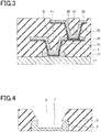
- Fig. 3 is a partial enlarged cross-sectional view of an example of multilayer wiring board according to the present embodiment.
- Fig. 3 illustrates a case where a via hole is a conformal via.
- the present invention can be implemented even in a case where the via hole is a filled via.
- a core substrate 1 is obtained by forming an insulating material such as glass epoxy resin, glass, or ceramic in a plate shape.
- the multilayer wiring board has three conductive layers (metallic wiring layers) formed on one side (upper surface in Fig. 1 ) of the core substrate 1. Specifically, on the upper surface of the core substrate 1, a first metallic wiring layer, a second metallic wiring layer, and a third metallic wiring layer, which are made of, for example, copper are laminated in this order with insulating layers interposed therebetween.
- Fig. 3 illustrates a structure having the core substrate 1.
- the multilayer wiring board of the present invention is also applicable to a structure without a core substrate, that is, a structure having wiring layers stacked on an interposer.
- the method of producing the first metallic wiring layer 21 is not particularly limited. However, a semi-additive process is preferable in that a substrate with high wiring density can be produced in a simple manner.
- a first seed layer is formed on the core substrate 1 by sputter coating of Ti and Cu, electroless Ni plating, Cu plating, or the like, and a photoresist layer is formed on the first seed layer.
- the photoresist may be a positive or negative liquid resist or a dry film resist.
- the photoresist is preferably a dry film resist because it is convenient and less expensive.
- the resist layer After being formed, the resist layer is exposed to light to form a first plated resin pattern thereon using a photomask in which a desired wiring pattern is drawn or a direct imaging apparatus for directly transferring a desired wiring pattern to the resist layer.
- electrolytic copper plating is performed. Then, the first plated resist pattern that is no longer needed is removed, and the first seed layer that is no longer needed is etched away to form the first metallic wiring layer 21.
- an insulating layer 3 is formed on the first metallic wiring layer 21.
- the insulating layer 3 is formed of a resin material such as a photosensitive polyimide resin, a photosensitive polybenzoxazole resin, a polyimide resin, an epoxy resin, a bismaleimide triazine resin, a cyanate resin, a polyphenylene oxide, a liquid crystal polymer, or a silicone resin, or a composite material of these materials.
- a resin material such as a photosensitive polyimide resin, a photosensitive polybenzoxazole resin, a polyimide resin, an epoxy resin, a bismaleimide triazine resin, a cyanate resin, a polyphenylene oxide, a liquid crystal polymer, or a silicone resin, or a composite material of these materials.
- a photosensitive polyimide resin or a photosensitive polybenzoxazole resin is preferable in that the formation of a fine pattern with excellent heat resistance and electrical characteristics is easy.
- the insulating layer 3 may preferably have a thickness in the range of 0.5 ⁇ m or more and 30 ⁇ m or less. If the thickness of the insulating layer 3 is smaller than 0.5 ⁇ m, the reliability of insulation between the metallic wiring layers may be deteriorated. On the other hand, if the thickness of the insulating layer 3 is larger than 30 ⁇ m, it is disadvantageous for forming a fine circuit.
- the method for forming the insulating layer 3 on the core substrate 1 may be roll lamination, vacuum lamination, or the like. If the insulating layer 3 is produced from a liquid varnish, the insulating layer 3 can be formed by a known method such as spin coating, die coating, curtain coating, or roller coating.
- a via hole 41 is formed for electrically connecting the first metallic wiring layer 21 and the second metallic wiring layer 22.
- the via hole 41 is formed by photolithography or by ablating the insulating layer 3 with a laser beam.
- the via hole may have a diameter in the range of 2 ⁇ m or more and 100 ⁇ m or less. If the diameter of the via hole is smaller than 2 ⁇ m, the reliability of the via connections may be deteriorated. On the other hand, if the diameter of the via hole is larger than 100 ⁇ m, it is disadvantageous for forming a fine circuit.
- oxygen plasma treatment is applied to the insulating layer 3 in which the via hole 41 is formed.
- a treatment for removing smears from the bottom surface of the via hole 41 and roughening the surface of the insulating layer 3 is applied.
- the metallic wiring pattern exposed on the bottom surface of the via hole is etched away to form a concave portion 7 as illustrated in Fig. 4 or Fig. 7 in the top surface of the first metallic wiring layer 21.
- the etching is preferably dry etching by an ion gun or Ar plasma because the concave portion can be formed with high yield.
- the concave portion 7 formed in the first metallic wiring layer 21 is preferably etched perpendicularly to the core substrate 1.
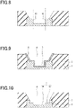
- the angle of a wall surface of the concave portion 7 is an angle A1 illustrated in Fig. 5 or an angle A2 illustrated in Fig.8 .
- the angle A1 is an angle formed between the wall surface of the concave portion 7 of the metallic wiring layer on the bottom surface of the via hole and the metallic wiring-insulating layer interface (synonymous with the upper surface of the core substrate 1).
- the angle A2 is an angle formed between the wall surface of the concave portion 7 of the metallic wiring layer on the bottom surface of the via hole and the upper surface of the core substrate 1.
- the angle A1 or A2 is preferably in the range of 75 degrees or more and 105 degrees or less.
- the angle A1 or A2 is smaller than 75 degrees, in a case when the insulating layer thermally expands and contracts, the force applied to the horizontal direction of the wiring board cannot be reduced, and thus the effect of preventing the removal of the via hole plated layer and the metallic wiring layer on the bottom surface of the via hole may be deteriorated.
- the angle A1 or A2 is larger than 105 degrees, the dissimilar metallic layer to be formed in the next step may not be continuously formed on the wall surface of the concave portion.
- the angle A1 or A2 is preferably closer to 90 degrees than the inclination angle along the axial direction of a wall surface of a via hole, in side view.
- the concave portion 7 formed on the bottom portion of the via hole by the dry etching may preferably have a depth in the range of 10 nm or more and 500 nm or less. If the depth of the concave portion is smaller than 10 nm, the depth of the concave portion embedded in the metallic wiring layer on the bottom surface of the via hole becomes smaller, and thus the effect of preventing the removal of the via hole plated layer and the metallic wiring layer on the bottom surface of the via hole may be deteriorated. On the other hand, if the depth of the concave portion is larger than 500 nm, the amount of dry etching becomes large, which makes it difficult to form the concave portion with high yield.
- the concave portion may more preferably have a depth in the range of 50 nm or more and 500 nm or less.
- Fig. 4 is a partial enlarged cross-sectional view of the bottom portion of the via hole of the multilayer wiring board of the present embodiment.
- the bottom end portion of the wall surface of the via hole and the upper end portion of the wall surface of the concave portion 7 formed in the metallic wiring layer on the bottom surface of the via hole become directly continuous without any level difference therebetween, as illustrated in Fig. 4 .
- the opening in the bottom surface of the via hole and the opening of the concave portion 7 formed in the metallic wiring layer on the bottom surface of the via hole have the same diameter and shape.
- Fig. 7 is a partial enlarged cross-sectional view of another bottom portion of the via hole of the multilayer wiring board of the present embodiment.
- the area of the opening in the bottom surface of the via hole may be larger than the cross-sectional area of the opening of the concave portion 7 formed in the upper surface of the metallic wiring layer on the bottom surface of the via hole.
- the width of the concave portion 7 may be smaller than the diameter of the bottom surface of the via hole.
- the bottom end portion of the wall surface of the via hole is arranged outside the upper end portion of the wall surface of the concave portion 7 formed in the metallic wiring layer.
- the bottom end portion of the wall surface of the via hole and the upper end portion of the wall surface of the concave portion 7 indirectly connect via the upper surface of the metallic wiring layer.
- the dissimilar metallic layer 5 can be formed uniformly on the wall surface of the via hole 4 and the concave portion 7 on the bottom surface of the via hole.
- the via hole in which the concave portion 7 is formed may be immersed in oxygen plasma or an etching liquid to etch the insulating layer 3 arranged on the wall surface of the via hole.
- the opening diameter of the concave portion formed in the metallic wiring pattern on the bottom surface of the via hole with respect to the opening diameter of the bottom surface of the via hole is preferably in the range of 50% or more and 100% or less. If the ratio of the opening diameter is not in the range of 50% or more and 100% or less, it may be difficult to form the dissimilar metallic layer on the concave portion.
- Fig. 10 is a partial enlarged cross-sectional view of another via hole bottom portion of the multilayer wiring board of the present embodiment.
- Fig. 10 illustrates an example of the concave portion 7 having a multilevel structure in which the cross-sectional area of the opening of the concave portion increases stepwisely from the bottom surface of the concave portion toward the via hole arranged above the concave portion.
- the concave portion 7 may have a multilevel structure in which the opening width becomes narrow, like a stair, toward the lower portion (the bottom side).
- a concave shape consisting of an upper first concave portion 71 and a lower second concave portion 72 may be formed in the metallic wiring layer 2 on the bottom surface of the via hole.
- the wall surface of the first concave portion 71 become continuous with the wall surface of the via hole 4, thereby forming the second concave portion 72 in the first concave portion 71.
- the dissimilar metallic layer 5 can be formed more uniformly on the wall surface of the via hole and the concave portion 7 on the bottom surface of the via hole. Because the contact area between the metallic wiring layer 2 and the dissimilar metallic layer 5 on the bottom surface of the via hole becomes large, the reliability of the via connections can be improved.
- a forming method can be such as forming an etching resist pattern after the via hole formation so that only the desired part is etched.
- the ratio of the opening diameter of the second concave portion 72 relative to the first concave portion 71 is preferably in the range of 50% or more and 100% or less. If the ratio of the opening diameter is not in the range of 50% or more and 100% or less, it may be difficult to form the dissimilar metallic layer on the concave portion 7.
- the second concave portion 72 is vertically etched.
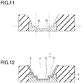
- the angle, such as angle A3 illustrated in Fig. 11 , formed between the wall surface of the second concave portion 72 of the metallic wiring layer on the bottom surface of the via hole and the metallic wiring layer parallel to the upper surface of the core substrate is in a range of 75 degrees or more and 105 degrees or less. If the angle A3 is smaller than 75 degrees, when the insulating layer thermally expands and contracts, the force applied to the horizontal direction of the wiring board cannot be reduced, and thus the effect of preventing the removal of the via hole plated layer and the metallic wiring layer on the bottom surface of the via hole may be deteriorated. On the other hand, if the angle A3 is larger than 105 degrees, the dissimilar metallic layer to be formed in the next step may not be continuously formed on the wall surface of the second concave portion.
- the second concave portion 72 may preferably have a depth in the range of 10 nm or more and 500 nm or less. If the depth of the second concave portion 72 is smaller than 10 nm, the depth of the second concave portion embedded in the metallic wiring layer 2 on the bottom surface of the via hole may become shallow, and thus the effect of preventing the removal of the via hole plated layer 61 and the metallic wiring layer 2 on the bottom surface of the via hole may be deteriorated. On the other hand, if the depth of the second concave portion 72 is larger than 500 nm, the amount of dry etching becomes large, which makes it difficult to form the second concave portion 72 with high yield.
- the second concave portion 72 may more preferably have a depth in the range of 50 nm or more and 500 nm or less.
- the dissimilar metallic layer 51 is formed on the bottom surface and inner wall surface of the via hole in which the concave portion 7 is formed, and on the surface of the insulating layer.
- the dissimilar metallic layer may be Ti, Ni, Ag, Sn, Au, or the like, but Ti is preferable because of its high strength and resistance to thermal expansion and contraction.
- the method for forming the dissimilar metallic layer 5 may be sputtering, CVD, vapor deposition, ion plating, electroless plating, or the like, but sputtering is convenient and practical.
- the via hole plated layer 61 and the second metallic wiring layer 22 are produced.
- the method for producing the via hole plated layer 61 and the second metallic wiring layer 22 is not particularly limited. However, a semi-additive process is preferable in that a substrate with high wiring density can be produced in a simple manner. An example of the production method will be described.
- the formed dissimilar metallic layer 51 is used as a seed layer for forming a photoresist layer on the dissimilar metallic layer.
- the photoresist layer is exposed to light to form a first plated resin pattern thereon using a photomask in which a desired wiring pattern is drawn or a direct imaging apparatus for transferring a desired wiring pattern to the photoresist layer.
- the plated resist pattern After the plated resist pattern is formed, electrolytic copper plating is performed, and the unnecessary portions of the plated resist pattern is removed.
- the upper portion of the dissimilar metallic layer 51 where no wiring pattern is formed becomes unnecessary and thus is removed by etching. Accordingly, the via hole plated layer 61 and the second metallic wiring layer 22 are formed.
- the insulating layer 3 is formed, and then the via hole 42 is formed for electrically connecting the second metallic wiring layer 22 and the third metallic wiring layer 23. Further, oxygen plasma treatment is applied to the insulating layer 3 in which the via hole 42 is formed. Then, a treatment for removing smears from the bottom surface of the via hole and for roughening the insulating layer surface is applied, followed by etching the metallic wiring pattern exposed on the bottom surface of the via hole, thereby forming a concave portion in the second metallic wiring layer 22.
- the dissimilar metallic layer 52 is formed on the bottom surface and the inner wall surface of the via hole having the concave portion and on the surface of the insulating layer, and then the via hole plated layer 62 and the third metallic wiring layer 23 are produced.
- a photoresist layer is formed on the dissimilar metallic layer. Then, the photoresist layer is exposed to light to form a first plated resin pattern thereon using a photomask in which a desired wiring pattern is drawn or a direct imaging apparatus for transferring a desired wiring pattern to the photoresist layer. After the plated resist pattern is formed, electrolytic copper plating is performed on the plated resist pattern to remove unnecessary portions from the plated resist pattern. Then, the upper portion of the dissimilar metallic layer 52 where no wiring pattern is formed becomes unnecessary and thus is removed by etching. Accordingly, the via hole plated layer 62 and the third metallic wiring layer 23 are formed.
- the thermal stress due to thermal expansion and contraction in the horizontal direction of the multilayer wiring board is also applied to the via hole plated layer formed on the inner wall surface of the via hole 4, and a load which might result in ruptures will be applied to this plated layer.
- the via hole plated layer is formed on the dissimilar metallic layer 5, and further, the dissimilar metallic layer 5 is embedded into the metallic wiring layer 2 on the bottom surface of the via hole. Accordingly, the via hole plated layer and the metallic wiring layer on the bottom surface of the via hole engage with each other with the dissimilar metallic layer interposed therebetween. This prevents the removal of the via hole plated layer and the metallic wire joint portion at via hole bottom. Therefore, in the present embodiment, it is possible to improve reliability of connection between the metallic wiring layers.
- the multilayer wiring board of the present embodiment as above can achieve excellent working effects as described below.
- the multilayer wiring board is configured such that a plurality of metallic wiring layers alternately laminated with an insulating layer interposed therebetween are electrically connected to each other via a via hole plated layer formed on a surface of a via hole.
- the multilayer wiring board includes a dissimilar metallic layer, made from material different from that of the metallic wiring layers, interposed between each of the metallic wiring layers on the bottom surface of the via hole and the via hole plated layer.
- a concave portion is formed in each of the metallic wiring layers on the bottom surface of the via hole at a position in contact with the dissimilar metallic layer.
- the dissimilar metallic layer is arranged in a concave shape on a surface of the concave portion formed in each of the metallic wiring layers on the bottom surface of the via hole.
- the multilayer wiring board in which the metallic wiring layers sandwiching the insulating layers are electrically connected to each other with the via hole plated layer interposed therebetween, at least one type of dissimilar metallic layer is formed in a concave shape between the metallic wiring layer on the bottom surface of the via hole and the via hole plated layer.
- the dissimilar metallic layer is embedded in the metallic wiring layer on the bottom surface of the via hole.
- the dissimilar metallic layer may preferably have a thickness in the range of 5 nm or more and 100 nm or less.
- the concave portion may preferably have a depth in the range of 10 nm or more and 500 nm or less.
- the angle of the wall surface of the concave portion with respect to the surface of the substrate on which the metallic wiring layers are formed is preferably in the range of 75 degrees or more and 105 degrees or less.
- At least a part of the dissimilar metallic layer may be formed on the surface of the via hole.
- the at least part of the dissimilar metallic layer including a first layer and a second layer.
- the first layer formed on the concave portion may be electrically connected to the second layer formed on the wall surface of the via hole.
- the bottom end portion of the wall surface of the via hole formed in the insulating layer may be directly continuous with the upper end portion of the concave portion.
- the via hole has an opening in the bottom of the via hole formed in the insulating layer which is wider than an opening of the concave portion.
- the dissimilar metallic layer including the first layer, the second layer, and a third layer.
- the first layer formed on the concave portion and the second layer formed on the wall surface of the via hole may be electrically connected via the third layer formed on the upper surface of the metallic wiring layer on the bottom surface of the via hole.
- the concave portion may have a multilevel structure in which the cross-sectional area of the opening of the concave portion increases stepwisely from the bottom surface of the concave portion toward the via hole.
- the multilevel structure is a two-level structure.
- each of the metallic wiring layer and the via hole plated layer may contain copper as a material.
- the dissimilar metallic layer may contain titanium as a material.
- the dissimilar metallic layer may contain nickel as a material.
- the above-described multilayer wiring board is produced, for example, as described below.
- a method for producing a multilayer wiring board employed in the present embodiment includes the steps of: forming a first seed layer by performing sputtering on a main surface that is a surface of a core substrate; forming a first plated resist pattern on the first seed layer; forming a first metallic wiring layer by electrolytic plating; removing the first plated resist pattern from the first seed layer; etching the first seed layer other than the first metallic wiring layer; forming an insulating layer to cover the first metallic wiring layer; forming a bottomed hole in a portion of the insulating layer which is located on the first metallic wiring layer, the bottomed hole to be a via hole and having an opening to partially expose an upper portion of the first metallic wiring layer; applying oxygen plasma treatment to the upper portion of the first metallic wiring layer, which is exposed, to clean the opening; applying argon ion gun treatment to the opening, which is cleaned, and etch the first metallic wiring layer in the opening to form a concave portion at a bottom of the opening; forming a second seed layer
- a method for producing a multilayer wiring board employed in the present embodiment includes the steps of: forming a first seed layer by performing sputtering on a main surface that is a surface of a core substrate; forming a first plated resist pattern on the first seed layer; forming a first metallic wiring layer by electrolytic plating; removing the first plated resist pattern from the first seed layer; etching the first seed layer other than the first metallic wiring layer; forming an insulating layer to cover the first metallic wiring layer; forming a bottomed hole in a portion of the insulating layer which is located on the first metallic wiring layer, the bottomed hole to be a via hole and having an opening to partially expose an upper portion of the first metallic wiring layer; applying oxygen plasma treatment to the upper portion of the first metallic wiring layer, which is exposed, to clean the opening; performing reverse sputtering on the opening, which is cleaned, and etch the first metallic wiring layer in the opened portion to form a concave portion at a bottom of the opened portion; forming a
- first seed layers 8 and 8A are formed on both sides of the core substrate 1.
- the first seed layers were formed using a sputtering apparatus, which is a film forming device that utilizes the phenomenon of solid materials ejecting from a solid surface by colliding the ionized and accelerated atoms or molecules with a specimen surface. Then, 300 nm thick Cu films were formed as the first seed layers 8 and 8A on the core substrate 1.
- first plated resist patterns 9 and 9A are formed on the first seed layers 8 and 8A.
- the resist patterns were each formed by laminating a dry film resist of 25 ⁇ m thickness, exposing the resist to light using a photomask in which a pattern corresponding to a wiring circuit was drawn, and then subjecting the resist to spray development with a 1% sodium carbonate water solution. Accordingly, the first plated resist patterns 9 and 9A were formed on the core substrate 1.
- the substrate was coated with electrolytic copper plating of 1 ⁇ m thickness using the first seed layers as power feed layers. Then, the first plated resist patterns that are no longer needed were removed by spraying a 3% sodium hydroxide solution at 60°C. Further, the unnecessary portions of the first seed layers were removed by a sulfuric acid and hydrogen peroxide aqueous solution, thereby forming first metallic wiring layers 21 and 21A.
- insulating layers 3 and 3A and via holes 4 and 4A were formed.
- the wiring substrate on which the first metallic wiring layers 21 and 21A are formed was immersed in a 10% sulfate solution and cleansed, and was coated with HD-4104 (produced by Hitachi Chemical DuPont Microsystems Ltd) by spin coating and was prebaked.
- the substrate was exposed to light except for the portions corresponding to the via holes 4 and 4A by using a direct imaging apparatus, and was subjected to organic development and cured, thereby forming the insulating layers 3 and 3A of 5 ⁇ m thickness and the via holes 4 and 4A.
- oxygen plasma treatment is performed, and a treatment for removing smears from the bottom portion of the via holes 4 and 4A and for roughening the surfaces of the insulating layers is applied.
- argon ion gun treatments (dry etching treatments) 10 and 10A were applied to the front and back surfaces of the wiring board to form concave portions 7 and 7A in the first metallic wiring layers 21 and 21A exposed from the bottom portions of the via hole. Subsequently, dissimilar metallic layers 5 and 5A were formed on the via holes 4 and 4A in which the concave portions 7 and 7A are formed at the bottom portions of the via hole, and on the surfaces of the insulating layers.
- dissimilar metallic layers 5 and 5A 50 nm thick Ti films were formed using a sputtering apparatus, and the dissimilar metallic layers 5 and 5A were used as seed layers for electrolytic copper plating. In this manner, the dissimilar metallic layers 5 and 5A were embedded in the first metallic wiring layers 21 and 21A at the bottoms of the via holes.
- second plated resist patterns 11 and 11 A are formed by laminating a dry film resist of 25 ⁇ m thickness on the dissimilar metal layer 5, performing exposure processing using a photomask in which a pattern corresponding to a wiring circuit is drawn, and then performing spray development processing with a 1% sodium carbonate aqueous solution.
- the wiring substrate on which the second plated resist patterns were formed was coated with electrolytic copper plating of 15 ⁇ m thickness using the dissimilar metallic layers 5 and 5A as power feed layers. Then, the second plated resist patterns that are no longer needed were removed by spraying a 3% sodium hydroxide aqueous solution at 60°C. Further, unnecessary portions of the dissimilar metallic layers 5 and 5A were removed by a Ti etching solution, thereby forming via hole plated layers 6 and 6A in the via holes in which concave portions are formed simultaneously when forming second metallic wiring layers 22 and 22A.
- the multilayer wiring board of the example has been described in the case where the metallic wiring layers has four metallic wiring layers, it can be widely applied to wiring boards with even more layers, such as six or eight metal wiring layers.
Landscapes
- Engineering & Computer Science (AREA)
- Microelectronics & Electronic Packaging (AREA)
- Manufacturing & Machinery (AREA)
- Production Of Multi-Layered Print Wiring Board (AREA)
Abstract
Description
- The present invention relates to a technique for multilayer wiring boards.
- Multilayer wiring boards are sometimes used as wiring boards for various types of electrical products. The multilayer wiring boards are designed on request to increase the circuit density to have an increased number of circuit patterns in the form of an insulating resin interposed between the layers of each circuit pattern. As this type of multilayer wiring board, there is known a method of forming a bottomed hole (via hole) in an insulating layer on a substrate, and electrically connecting circuit patterns on different layers (metallic wiring layers) via the bottomed hole.
- This type of multilayer circuit board is configured such that conductive layers (metallic wiring layers) and insulating layers are alternately laminated. The circuit patterns on the conductive layers are electrically connected at interlayer connection portions formed by making holes in the insulating layers between the circuit patterns as necessary.
-
Figs. 1 and 2 are enlarged cross-sectional views of examples of the conventional multilayer wiring board described above. -
Fig. 1 is an enlarged cross-sectional view of a multilayer wiring board in which circuit patterns on layers (a firstmetallic wiring layer 21, a secondmetallic wiring layer 22, and a third metallic wiring layer 23) and interlayer connection wires (a first via hole platedlayer 61 and a second via hole plated layer 62) are formed of the same type of metallic material.Fig. 2 is an enlarged cross-sectional view of a multilayer wiring board formed of two or more types of metallic materials.Figs. 1 and 2 show multilayer wiring boards in which three conductive layers are formed on one side of multilayer wiring board. - The electrical connection between the conductive layers in
Figs. 1 and 2 is achieved by forming viaholes insulating layers 3 with a laser beam to reach a target that is the conductive layer, and forming the via hole platedlayers via holes Figs. 1 and 2 , the firstmetallic wiring layer 21, the secondmetallic wiring layer 22, and the thirdmetallic wiring layer 23 are electrically connected via the via hole platedlayers - A seed layer serving as a power supply layer for plating is required for forming the via hole plated
layers Fig. 1 , the seed layer is made from material same as that of the wiring material, whereas in the example shown inFig. 2 , the seed layer is made from material different from that of the wiring material. - In recent years, there has been a demand for smaller, thinner multilayer wiring boards and finer wiring line widths. Thus, wiring layers are generally formed by forming films of metals different from a wiring material (a first dissimilar
metallic layer 51 and a second dissimilar metallic layer 52) on the seed layers of electrolytic plating, as illustrated inFig. 2 , by dry processing such as sputter coating. - In the case of forming films of metals different from the wiring material onto the seed layers of electrolytic plating as illustrated in
Fig. 2 , the wiring layers at the bottom portions of thevia holes metallic layers Fig. 2 , cracks or ruptures may occur at the interface between the dissimilarmetallic layer 51 and the firstmetallic wiring layer 21 at the bottom portion of the via hole, and at the interface between the dissimilarmetallic layer 52 and the secondmetallic wiring layer 22, because of thermal stress occurring due to differences in thermal expansion coefficients between the insulating layers and the metallic wiring layers. The configuration shown inFig. 2 requires improvement in the connection reliability of the via connections. - For solving the problem of thermal stress applied to such via holes, for example, there have been conventionally suggested techniques described in
PTL 1 andPTL 2.PTL 1 discloses a multilayer wiring board having at least one through hole filled with low modulus filler around a via hole for electrically connecting the metallic wiring layers with insulating layers interposed therebetween, and a method of producing the same.PTL 2 discloses a multilayer wiring board in which one or more dummy via holes not connected to a circuit pattern are formed near a via hole, and a method of producing the same. -
- [PTL 1]
JP 2002-314256 A - [PTL 2]
JP 2002-319767 A - However, in
PTL 1 andPTL 2, there is a problem that through holes or non-through holes which does not involve in electrical connection must be formed, which increases the complexity of the producing process. - The present invention has been devised in view of the foregoing problem, and an object of the present invention is to improve the reliability of connection of via hole connection portions in a simpler manner.
- To solve the problem, an aspect of the present invention is to provide a multilayer wiring board comprising a plurality of metallic wiring layers alternately laminated with an insulating layer interposed therebetween are electrically connected to each other via a via hole plated layer formed on a surface of a via hole. The multilayer wiring board includes a dissimilar metallic layer, made from material different from that of the metallic wiring layers, interposed between each of the metallic wiring layers on the bottom surface of the via hole and the via hole plated layer. A concave portion is formed in each of the metallic wiring layers on the bottom surface of the via hole at a position in contact with the dissimilar metallic layer. The dissimilar metallic layer is arranged in a concave shape on a surface of the concave portion formed in each of the metallic wiring layers on the bottom surface of the via hole.
- According to the aspect of the present invention, it is possible to provide a multilayer wiring board in which the connection reliability of the via hole connection portion is improved in a simpler manner.
-
-
Fig. 1 is an enlarged cross-sectional view of a multilayer wiring board in which circuit patterns on layers and interlayer connection wires are formed of the same type of metallic material, in a conventional example. -
Fig. 2 is an enlarged cross-sectional view of a multilayer wiring board formed of two or more types of metallic material in a conventional example. -
Fig. 3 is a partial enlarged cross-sectional view of an example of a multilayer wiring board according to an embodiment of the present invention. -
Fig. 4 is a partial enlarged cross-sectional view of a bottom portion of a via hole in a multilayer wiring board according to an embodiment of the present invention. -
Fig. 5 is a partial enlarged cross-sectional view of a bottom portion of a via hole in a multilayer wiring board according to an embodiment of the present invention. -
Fig. 6 is a partial enlarged cross-sectional view of a bottom portion of a via hole in a multilayer wiring board according to an embodiment of the present invention. -
Fig. 7 is a partial enlarged cross-sectional view of a bottom portion of a via hole in a multilayer wiring board according to an embodiment of the present invention. -
Fig. 8 is a partial enlarged cross-sectional view of a bottom portion of a via hole in a multilayer wiring board according to an embodiment of the present invention. -
Fig. 9 is a partial enlarged cross-sectional view of a bottom portion of a via hole in a multilayer wiring board according to an embodiment of the present invention. -
Fig. 10 is a partial enlarged cross-sectional view of a bottom portion of a via hole in a multilayer wiring board according to an embodiment of the present invention. -
Fig. 11 is a partial enlarged cross-sectional view of a bottom portion of a via hole in a multilayer wiring board according to an embodiment of the present invention. -
Fig. 12 is a partial enlarged cross-sectional view of a bottom portion of a via hole in a multilayer wiring board according to an embodiment of the present invention. -
Figs. 13(A) to 13(1) are explanatory diagrams describing an example of a multilayer wiring board. - Hereinafter, an embodiment of the present invention will be described with reference to the drawings.
-
Fig. 3 is a partial enlarged cross-sectional view of an example of multilayer wiring board according to the present embodiment. -
Fig. 3 illustrates a case where a via hole is a conformal via. However, the present invention can be implemented even in a case where the via hole is a filled via. - Similar components to those in the conventional structure described above will be described with the same reference signs.
- A
core substrate 1 is obtained by forming an insulating material such as glass epoxy resin, glass, or ceramic in a plate shape. - In the example shown in
Fig. 3 , the multilayer wiring board has three conductive layers (metallic wiring layers) formed on one side (upper surface inFig. 1 ) of thecore substrate 1. Specifically, on the upper surface of thecore substrate 1, a first metallic wiring layer, a second metallic wiring layer, and a third metallic wiring layer, which are made of, for example, copper are laminated in this order with insulating layers interposed therebetween.Fig. 3 illustrates a structure having thecore substrate 1. However, the multilayer wiring board of the present invention is also applicable to a structure without a core substrate, that is, a structure having wiring layers stacked on an interposer. - The method of producing the first
metallic wiring layer 21 is not particularly limited. However, a semi-additive process is preferable in that a substrate with high wiring density can be produced in a simple manner. To explain an example of the production method, a first seed layer is formed on thecore substrate 1 by sputter coating of Ti and Cu, electroless Ni plating, Cu plating, or the like, and a photoresist layer is formed on the first seed layer. The photoresist may be a positive or negative liquid resist or a dry film resist. However, the photoresist is preferably a dry film resist because it is convenient and less expensive. After being formed, the resist layer is exposed to light to form a first plated resin pattern thereon using a photomask in which a desired wiring pattern is drawn or a direct imaging apparatus for directly transferring a desired wiring pattern to the resist layer. After the first plated resist pattern is formed, electrolytic copper plating is performed. Then, the first plated resist pattern that is no longer needed is removed, and the first seed layer that is no longer needed is etched away to form the firstmetallic wiring layer 21. - Next, in the present embodiment, an insulating
layer 3 is formed on the firstmetallic wiring layer 21. - The insulating
layer 3 is formed of a resin material such as a photosensitive polyimide resin, a photosensitive polybenzoxazole resin, a polyimide resin, an epoxy resin, a bismaleimide triazine resin, a cyanate resin, a polyphenylene oxide, a liquid crystal polymer, or a silicone resin, or a composite material of these materials. The use of a photosensitive polyimide resin or a photosensitive polybenzoxazole resin is preferable in that the formation of a fine pattern with excellent heat resistance and electrical characteristics is easy. - Although not particularly limited, the insulating
layer 3 may preferably have a thickness in the range of 0.5 µm or more and 30 µm or less. If the thickness of the insulatinglayer 3 is smaller than 0.5 µm, the reliability of insulation between the metallic wiring layers may be deteriorated. On the other hand, if the thickness of the insulatinglayer 3 is larger than 30 µm, it is disadvantageous for forming a fine circuit. - If the insulating
layer 3 is in a sheet form, the method for forming the insulatinglayer 3 on thecore substrate 1 may be roll lamination, vacuum lamination, or the like. If the insulatinglayer 3 is produced from a liquid varnish, the insulatinglayer 3 can be formed by a known method such as spin coating, die coating, curtain coating, or roller coating. - Next, a via
hole 41 is formed for electrically connecting the firstmetallic wiring layer 21 and the secondmetallic wiring layer 22. The viahole 41 is formed by photolithography or by ablating the insulatinglayer 3 with a laser beam. - Although not particularly limited, the via hole may have a diameter in the range of 2 µm or more and 100 µm or less. If the diameter of the via hole is smaller than 2 µm, the reliability of the via connections may be deteriorated. On the other hand, if the diameter of the via hole is larger than 100 µm, it is disadvantageous for forming a fine circuit.
- Next, oxygen plasma treatment is applied to the insulating
layer 3 in which the viahole 41 is formed. Then, a treatment for removing smears from the bottom surface of the viahole 41 and roughening the surface of the insulatinglayer 3 is applied. Thereafter, the metallic wiring pattern exposed on the bottom surface of the via hole is etched away to form aconcave portion 7 as illustrated inFig. 4 orFig. 7 in the top surface of the firstmetallic wiring layer 21. The etching is preferably dry etching by an ion gun or Ar plasma because the concave portion can be formed with high yield. Theconcave portion 7 formed in the firstmetallic wiring layer 21 is preferably etched perpendicularly to thecore substrate 1. The angle of a wall surface of theconcave portion 7 is an angle A1 illustrated inFig. 5 or an angle A2 illustrated inFig.8 . The angle A1 is an angle formed between the wall surface of theconcave portion 7 of the metallic wiring layer on the bottom surface of the via hole and the metallic wiring-insulating layer interface (synonymous with the upper surface of the core substrate 1). The angle A2 is an angle formed between the wall surface of theconcave portion 7 of the metallic wiring layer on the bottom surface of the via hole and the upper surface of thecore substrate 1. The angle A1 or A2 is preferably in the range of 75 degrees or more and 105 degrees or less. If the angle A1 or A2 is smaller than 75 degrees, in a case when the insulating layer thermally expands and contracts, the force applied to the horizontal direction of the wiring board cannot be reduced, and thus the effect of preventing the removal of the via hole plated layer and the metallic wiring layer on the bottom surface of the via hole may be deteriorated. On the other hand, if the angle A1 or A2 is larger than 105 degrees, the dissimilar metallic layer to be formed in the next step may not be continuously formed on the wall surface of the concave portion. - The angle A1 or A2 is preferably closer to 90 degrees than the inclination angle along the axial direction of a wall surface of a via hole, in side view.
- The
concave portion 7 formed on the bottom portion of the via hole by the dry etching may preferably have a depth in the range of 10 nm or more and 500 nm or less. If the depth of the concave portion is smaller than 10 nm, the depth of the concave portion embedded in the metallic wiring layer on the bottom surface of the via hole becomes smaller, and thus the effect of preventing the removal of the via hole plated layer and the metallic wiring layer on the bottom surface of the via hole may be deteriorated. On the other hand, if the depth of the concave portion is larger than 500 nm, the amount of dry etching becomes large, which makes it difficult to form the concave portion with high yield. The concave portion may more preferably have a depth in the range of 50 nm or more and 500 nm or less. -
Fig. 4 is a partial enlarged cross-sectional view of the bottom portion of the via hole of the multilayer wiring board of the present embodiment. By etching the metallic wiring pattern made of the metallic wiring layer exposed to the bottom surface of the via hole, the bottom end portion of the wall surface of the via hole and the upper end portion of the wall surface of theconcave portion 7 formed in the metallic wiring layer on the bottom surface of the via hole become directly continuous without any level difference therebetween, as illustrated inFig. 4 . For example, the opening in the bottom surface of the via hole and the opening of theconcave portion 7 formed in the metallic wiring layer on the bottom surface of the via hole have the same diameter and shape. When forming a dissimilarmetallic layer 5 on the wall surface of the via hole and on the bottom surface and the wall surface of theconcave portion 7 as illustrated inFig. 4 , the configuration illustrated inFig. 6 is obtained. - As another method, there is a structure as illustrated in
Fig. 7. Fig. 7 is a partial enlarged cross-sectional view of another bottom portion of the via hole of the multilayer wiring board of the present embodiment. - As illustrated in
Fig. 7 , the area of the opening in the bottom surface of the via hole may be larger than the cross-sectional area of the opening of theconcave portion 7 formed in the upper surface of the metallic wiring layer on the bottom surface of the via hole. - For example, the width of the
concave portion 7 may be smaller than the diameter of the bottom surface of the via hole. The bottom end portion of the wall surface of the via hole is arranged outside the upper end portion of the wall surface of theconcave portion 7 formed in the metallic wiring layer. Thus, the bottom end portion of the wall surface of the via hole and the upper end portion of the wall surface of theconcave portion 7 indirectly connect via the upper surface of the metallic wiring layer. - With the configuration as illustrated in
Fig. 7 , the dissimilarmetallic layer 5 can be formed uniformly on the wall surface of the viahole 4 and theconcave portion 7 on the bottom surface of the via hole. As a method for forming the dissimilarmetallic layer 5, the via hole in which theconcave portion 7 is formed may be immersed in oxygen plasma or an etching liquid to etch the insulatinglayer 3 arranged on the wall surface of the via hole. The opening diameter of the concave portion formed in the metallic wiring pattern on the bottom surface of the via hole with respect to the opening diameter of the bottom surface of the via hole is preferably in the range of 50% or more and 100% or less. If the ratio of the opening diameter is not in the range of 50% or more and 100% or less, it may be difficult to form the dissimilar metallic layer on the concave portion. - When forming the dissimilar
metallic layer 5 on the wall surface of the viahole 4 and on the bottom surface and wall surface of theconcave portion 7 as illustrated inFig. 7 , the configuration illustrated inFig. 9 is obtained. - As a still another method, there is a structure illustrated in
Fig. 10. Fig. 10 is a partial enlarged cross-sectional view of another via hole bottom portion of the multilayer wiring board of the present embodiment.Fig. 10 illustrates an example of theconcave portion 7 having a multilevel structure in which the cross-sectional area of the opening of the concave portion increases stepwisely from the bottom surface of the concave portion toward the via hole arranged above the concave portion. Theconcave portion 7 may have a multilevel structure in which the opening width becomes narrow, like a stair, toward the lower portion (the bottom side). For example, a concave shape consisting of an upper firstconcave portion 71 and a lower secondconcave portion 72 may be formed in themetallic wiring layer 2 on the bottom surface of the via hole. The wall surface of the firstconcave portion 71 become continuous with the wall surface of the viahole 4, thereby forming the secondconcave portion 72 in the firstconcave portion 71. With the configuration as illustrated inFig. 10 , the dissimilarmetallic layer 5 can be formed more uniformly on the wall surface of the via hole and theconcave portion 7 on the bottom surface of the via hole. Because the contact area between themetallic wiring layer 2 and the dissimilarmetallic layer 5 on the bottom surface of the via hole becomes large, the reliability of the via connections can be improved. In this case, a forming method can be such as forming an etching resist pattern after the via hole formation so that only the desired part is etched. The ratio of the opening diameter of the secondconcave portion 72 relative to the firstconcave portion 71 is preferably in the range of 50% or more and 100% or less. If the ratio of the opening diameter is not in the range of 50% or more and 100% or less, it may be difficult to form the dissimilar metallic layer on theconcave portion 7. - Preferably, the second
concave portion 72 is vertically etched. The angle, such as angle A3 illustrated inFig. 11 , formed between the wall surface of the secondconcave portion 72 of the metallic wiring layer on the bottom surface of the via hole and the metallic wiring layer parallel to the upper surface of the core substrate is in a range of 75 degrees or more and 105 degrees or less. If the angle A3 is smaller than 75 degrees, when the insulating layer thermally expands and contracts, the force applied to the horizontal direction of the wiring board cannot be reduced, and thus the effect of preventing the removal of the via hole plated layer and the metallic wiring layer on the bottom surface of the via hole may be deteriorated. On the other hand, if the angle A3 is larger than 105 degrees, the dissimilar metallic layer to be formed in the next step may not be continuously formed on the wall surface of the second concave portion. - The second
concave portion 72 may preferably have a depth in the range of 10 nm or more and 500 nm or less. If the depth of the secondconcave portion 72 is smaller than 10 nm, the depth of the second concave portion embedded in themetallic wiring layer 2 on the bottom surface of the via hole may become shallow, and thus the effect of preventing the removal of the via hole platedlayer 61 and themetallic wiring layer 2 on the bottom surface of the via hole may be deteriorated. On the other hand, if the depth of the secondconcave portion 72 is larger than 500 nm, the amount of dry etching becomes large, which makes it difficult to form the secondconcave portion 72 with high yield. The secondconcave portion 72 may more preferably have a depth in the range of 50 nm or more and 500 nm or less. When forming the dissimilarmetallic layer 5 on the wall surface of the via hole and on the bottom surface and wall surface of theconcave portion 7 as illustrated inFig. 10 , the configuration as illustrated inFig. 12 is obtained. - Next, the dissimilar
metallic layer 51 is formed on the bottom surface and inner wall surface of the via hole in which theconcave portion 7 is formed, and on the surface of the insulating layer. The dissimilar metallic layer may be Ti, Ni, Ag, Sn, Au, or the like, but Ti is preferable because of its high strength and resistance to thermal expansion and contraction. The method for forming the dissimilarmetallic layer 5 may be sputtering, CVD, vapor deposition, ion plating, electroless plating, or the like, but sputtering is convenient and practical. By forming the dissimilar metallic layer on the metallic wiring layer on the bottom surface of the via hole having theconcave portion 7, the dissimilar metallic layer having a concave shape is formed so as to be embedded in themetallic wiring layer 2 on the bottom surface of the via hole. - Next, the via hole plated
layer 61 and the secondmetallic wiring layer 22 are produced. The method for producing the via hole platedlayer 61 and the secondmetallic wiring layer 22 is not particularly limited. However, a semi-additive process is preferable in that a substrate with high wiring density can be produced in a simple manner. An example of the production method will be described. First, the formed dissimilarmetallic layer 51 is used as a seed layer for forming a photoresist layer on the dissimilar metallic layer. Next, the photoresist layer is exposed to light to form a first plated resin pattern thereon using a photomask in which a desired wiring pattern is drawn or a direct imaging apparatus for transferring a desired wiring pattern to the photoresist layer. After the plated resist pattern is formed, electrolytic copper plating is performed, and the unnecessary portions of the plated resist pattern is removed. The upper portion of the dissimilarmetallic layer 51 where no wiring pattern is formed becomes unnecessary and thus is removed by etching. Accordingly, the via hole platedlayer 61 and the secondmetallic wiring layer 22 are formed. - Next, the insulating
layer 3 is formed, and then the viahole 42 is formed for electrically connecting the secondmetallic wiring layer 22 and the thirdmetallic wiring layer 23. Further, oxygen plasma treatment is applied to the insulatinglayer 3 in which the viahole 42 is formed. Then, a treatment for removing smears from the bottom surface of the via hole and for roughening the insulating layer surface is applied, followed by etching the metallic wiring pattern exposed on the bottom surface of the via hole, thereby forming a concave portion in the secondmetallic wiring layer 22. - Next, the dissimilar
metallic layer 52 is formed on the bottom surface and the inner wall surface of the via hole having the concave portion and on the surface of the insulating layer, and then the via hole platedlayer 62 and the thirdmetallic wiring layer 23 are produced. - An example of production thereof will be described. First, using the formed dissimilar
metallic layer 52 as a seed layer, a photoresist layer is formed on the dissimilar metallic layer. Then, the photoresist layer is exposed to light to form a first plated resin pattern thereon using a photomask in which a desired wiring pattern is drawn or a direct imaging apparatus for transferring a desired wiring pattern to the photoresist layer. After the plated resist pattern is formed, electrolytic copper plating is performed on the plated resist pattern to remove unnecessary portions from the plated resist pattern. Then, the upper portion of the dissimilarmetallic layer 52 where no wiring pattern is formed becomes unnecessary and thus is removed by etching. Accordingly, the via hole platedlayer 62 and the thirdmetallic wiring layer 23 are formed. - When the thermal stress due to thermal expansion and contraction is applied to the multilayer wiring board of the present embodiment formed as above, the thermal stress due to thermal expansion and contraction in the horizontal direction of the multilayer wiring board is also applied to the via hole plated layer formed on the inner wall surface of the via
hole 4, and a load which might result in ruptures will be applied to this plated layer. In the present embodiment, the via hole plated layer is formed on the dissimilarmetallic layer 5, and further, the dissimilarmetallic layer 5 is embedded into themetallic wiring layer 2 on the bottom surface of the via hole. Accordingly, the via hole plated layer and the metallic wiring layer on the bottom surface of the via hole engage with each other with the dissimilar metallic layer interposed therebetween. This prevents the removal of the via hole plated layer and the metallic wire joint portion at via hole bottom. Therefore, in the present embodiment, it is possible to improve reliability of connection between the metallic wiring layers. - The multilayer wiring board of the present embodiment as above can achieve excellent working effects as described below.
- In the present embodiment, the multilayer wiring board is configured such that a plurality of metallic wiring layers alternately laminated with an insulating layer interposed therebetween are electrically connected to each other via a via hole plated layer formed on a surface of a via hole. The multilayer wiring board includes a dissimilar metallic layer, made from material different from that of the metallic wiring layers, interposed between each of the metallic wiring layers on the bottom surface of the via hole and the via hole plated layer. A concave portion is formed in each of the metallic wiring layers on the bottom surface of the via hole at a position in contact with the dissimilar metallic layer. The dissimilar metallic layer is arranged in a concave shape on a surface of the concave portion formed in each of the metallic wiring layers on the bottom surface of the via hole.
- According to this configuration, in the multilayer wiring board in which the metallic wiring layers sandwiching the insulating layers are electrically connected to each other with the via hole plated layer interposed therebetween, at least one type of dissimilar metallic layer is formed in a concave shape between the metallic wiring layer on the bottom surface of the via hole and the via hole plated layer. The dissimilar metallic layer is embedded in the metallic wiring layer on the bottom surface of the via hole. As a result, the metallic wiring layer on the bottom surface of the via hole and the via hole plated layer electrically connecting the wiring layers engage with each other with the dissimilar metallic layer interposed therebetween. This engagement prevents removal of the via hole plated layer from the metallic wiring layer on the bottom surface of the via hole, and improvement in the reliability of connection of the via hole connection portion.
- The dissimilar metallic layer may preferably have a thickness in the range of 5 nm or more and 100 nm or less.
- The concave portion may preferably have a depth in the range of 10 nm or more and 500 nm or less.
- The angle of the wall surface of the concave portion with respect to the surface of the substrate on which the metallic wiring layers are formed is preferably in the range of 75 degrees or more and 105 degrees or less.
- In the present embodiment, at least a part of the dissimilar metallic layer may be formed on the surface of the via hole. The at least part of the dissimilar metallic layer including a first layer and a second layer. The first layer formed on the concave portion may be electrically connected to the second layer formed on the wall surface of the via hole.
- In the present embodiment, the bottom end portion of the wall surface of the via hole formed in the insulating layer may be directly continuous with the upper end portion of the concave portion.
- In the present embodiment, the via hole has an opening in the bottom of the via hole formed in the insulating layer which is wider than an opening of the concave portion. The dissimilar metallic layer including the first layer, the second layer, and a third layer. The first layer formed on the concave portion and the second layer formed on the wall surface of the via hole may be electrically connected via the third layer formed on the upper surface of the metallic wiring layer on the bottom surface of the via hole.
- In the present embodiment, the concave portion may have a multilevel structure in which the cross-sectional area of the opening of the concave portion increases stepwisely from the bottom surface of the concave portion toward the via hole.
- For example, the multilevel structure is a two-level structure.
- In the present embodiment, each of the metallic wiring layer and the via hole plated layer may contain copper as a material.
- In the present embodiment, the dissimilar metallic layer may contain titanium as a material.
- In the present embodiment, the dissimilar metallic layer may contain nickel as a material.
- The above-described multilayer wiring board is produced, for example, as described below.
- A method for producing a multilayer wiring board employed in the present embodiment includes the steps of: forming a first seed layer by performing sputtering on a main surface that is a surface of a core substrate; forming a first plated resist pattern on the first seed layer; forming a first metallic wiring layer by electrolytic plating; removing the first plated resist pattern from the first seed layer; etching the first seed layer other than the first metallic wiring layer; forming an insulating layer to cover the first metallic wiring layer; forming a bottomed hole in a portion of the insulating layer which is located on the first metallic wiring layer, the bottomed hole to be a via hole and having an opening to partially expose an upper portion of the first metallic wiring layer; applying oxygen plasma treatment to the upper portion of the first metallic wiring layer, which is exposed, to clean the opening; applying argon ion gun treatment to the opening, which is cleaned, and etch the first metallic wiring layer in the opening to form a concave portion at a bottom of the opening; forming a second seed layer in a form of a dissimilar metallic layer on the insulating layer having the concave portion over the opening at the bottom, the dissimilar metallic layer being different in material from the first metallic wiring layer; forming a dissimilar metallic layer on the concave portion simultaneously when forming the second seed layer to make the dissimilar metallic layer having a concave shape; forming a second plated resist pattern on the second seed layer; forming a pattern of a second metallic wiring layer by electrolytic plating; and removing the second plated resist layer that is no longer needed after forming the pattern of the second metallic wiring layer and removing an unnecessary portion of the second seed layer by etching.
- Alternatively, a method for producing a multilayer wiring board employed in the present embodiment includes the steps of: forming a first seed layer by performing sputtering on a main surface that is a surface of a core substrate; forming a first plated resist pattern on the first seed layer; forming a first metallic wiring layer by electrolytic plating; removing the first plated resist pattern from the first seed layer; etching the first seed layer other than the first metallic wiring layer; forming an insulating layer to cover the first metallic wiring layer; forming a bottomed hole in a portion of the insulating layer which is located on the first metallic wiring layer, the bottomed hole to be a via hole and having an opening to partially expose an upper portion of the first metallic wiring layer; applying oxygen plasma treatment to the upper portion of the first metallic wiring layer, which is exposed, to clean the opening; performing reverse sputtering on the opening, which is cleaned, and etch the first metallic wiring layer in the opened portion to form a concave portion at a bottom of the opened portion; forming a second seed layer in a form of a dissimilar metallic layer on the insulating layer having the concave portion over the opening at the bottom, the dissimilar metallic layer being different in material from the first metallic wiring layer; forming a dissimilar metallic layer on the concave portion simultaneously when forming the second seed layer to make the dissimilar metallic layer having a concave shape; forming a second plated resist pattern on the second seed layer; forming a pattern of a second metallic wiring layer by electrolytic plating; and removing the second plated resist layer that is no longer needed after forming the pattern of the second metallic wiring layer and removing an unnecessary portion of the second seed layer by etching.
- Next, an example based on the present embodiment will be described with reference to
Figs. 13(A) to 13(1) . - In the present example, as illustrated in
Fig. 13(A) , thin metallic layers (first seed layers) 8 and 8A are formed on both sides of thecore substrate 1. The first seed layers were formed using a sputtering apparatus, which is a film forming device that utilizes the phenomenon of solid materials ejecting from a solid surface by colliding the ionized and accelerated atoms or molecules with a specimen surface. Then, 300 nm thick Cu films were formed as thefirst seed layers core substrate 1. - Next, as illustrated in
Fig. 13(B) , first plated resistpatterns first seed layers patterns core substrate 1. - As illustrated in
Fig. 13(C) , the substrate was coated with electrolytic copper plating of 1 µm thickness using the first seed layers as power feed layers. Then, the first plated resist patterns that are no longer needed were removed by spraying a 3% sodium hydroxide solution at 60°C. Further, the unnecessary portions of the first seed layers were removed by a sulfuric acid and hydrogen peroxide aqueous solution, thereby forming first metallic wiring layers 21 and 21A. - Next, as illustrated in
Figs. 13(D) and 13(E) , insulatinglayers holes layers - Next, as illustrated in
Figs. 13(F) and 13(G) , after the oxygen plasma treatment, argon ion gun treatments (dry etching treatments) 10 and 10A were applied to the front and back surfaces of the wiring board to formconcave portions metallic layers concave portions metallic layers metallic layers metallic layers - Next, as illustrated in
Fig. 13(H) , second plated resistpatterns dissimilar metal layer 5, performing exposure processing using a photomask in which a pattern corresponding to a wiring circuit is drawn, and then performing spray development processing with a 1% sodium carbonate aqueous solution. - Next, as illustrated in
Fig. 13(1) , the wiring substrate on which the second plated resist patterns were formed was coated with electrolytic copper plating of 15 µm thickness using the dissimilarmetallic layers metallic layers layers - The present invention is not limited to the example described above and illustrated in the drawings but can be modified in various forms without departing from the gist of the present invention.
- Although the multilayer wiring board of the example has been described in the case where the metallic wiring layers has four metallic wiring layers, it can be widely applied to wiring boards with even more layers, such as six or eight metal wiring layers.
- The scope of the present invention is not limited to the illustrative embodiment illustrated and described above, but also includes all embodiments that yield effects equivalent to the effects intended by the present invention. Furthermore, the scope of the present invention is not limited to combinations of features recited in the claims, but may be defined by any desired combination of specific features among all the disclosed features.
- This application claims the benefit of priority from
Japanese Patent Application No. 2019-102736 (filed on May 31, 2019 -
- 1..Core substrate (inner layer substrate)
- 2..Metallic wiring layer
- 21..First metallic wiring layer
- 22..Second metallic wiring layer
- 23..Third metallic wiring layer
- 3..Insulating layer
- 4..Via hole
- 41..First via hole
- 42..Second via hole
- 5..Dissimilar metallic layer
- 51..First dissimilar metallic layer
- 52..Second dissimilar metallic layer
- 6..Via hole plated layer
- 61..First via hole plated layer
- 62..Second via hole plated layer
- 7..Concave portion
- 71..First concave portion
- 72..Second concave portion
- 8..First seed layer
- 9..First plated resist pattern
- 10..Conceptual diagram of dry etching
- 11.. Second plated resist pattern
- A1..Angle formed between wall surface of concave portion of metallic wiring layer on bottom surface of via hole and metallic wiring-insulating layer interface
- A2..Angle formed between wall surface of concave portion of metallic wiring layer on bottom surface of via hole and metallic layer parallel to the direction of wiring board
- A3 ... Angle formed between wall surface of second concave portion of metallic wiring layer on bottom surface of via hole and metallic layer parallel to the direction of wiring board
Claims (14)
- A multilayer wiring board comprising a plurality of metallic wiring layers alternately laminated with an insulating layer interposed therebetween are electrically connected to each other via a via hole plated layer formed on a surface of a via hole, whereina dissimilar metallic layer, made from material different from that of the metallic wiring layers, is interposed between each of the metallic wiring layers on a bottom surface of the via hole and the via hole plated layer,a concave portion is formed in each of the metallic wiring layers on the bottom surface of the via hole at a position in contact with the dissimilar metallic layer, andthe dissimilar metallic layer is arranged in a concave shape on a surface of the concave portion which is formed in each of the metallic wiring layers on the bottom surface of the via hole.
- The multilayer wiring board according to claim 1, wherein the dissimilar metallic layer has a thickness in a range of 5 nm or more and 100 nm or less.
- The multilayer wiring board according to claim 1 or 2, wherein the concave portion has a depth in a range of 10 nm or more and 500 nm or less.
- The multilayer wiring board according to any one of claims 1 to 3, wherein an angle of a wall surface of the concave portion with respect to a surface of a substrate on which each of the metallic wiring layers are formed is in a range of 75 degrees or more and 105 degrees or less.
- The multilayer wiring board according to any one of claims 1 to 4, whereinat least a part of the dissimilar metallic layer is formed on the surface of the via hole, the at least part of the dissimilar metallic layer including a first layer and a second layer, andthe first layer formed on the concave portion is electrically connected to the second layer formed on the wall surface of the via hole.
- The multilayer wiring board according to any one of claims 1 to 5, wherein a bottom end portion of the wall surface of the via hole is directly continuous with an upper end portion of the concave portion.
- The multilayer wiring board according to claim 5, whereinthe via hole has an opening in a bottom thereof which is wider than an opening of the concave portion, andthe dissimilar metallic layer including the first layer, the second layer, and a third layer, the first layer formed on the concave portion and the second layer formed on the wall surface of the via hole are electrically connected via the third layer formed on an upper surface of each of metallic wiring layers on a bottom surface of the via hole.
- The multilayer wiring board according to any one of claims 1 to 5, wherein the concave portion has a multilevel structure in which a cross-sectional area of an opening of the concave portion increases stepwisely from a bottom surface of the concave portion toward the via hole.
- The multilayer wiring board according to claim 8, wherein the multilevel structure is a two-level structure.
- The multilayer wiring board according to any one of claims 1 to 9, wherein each of the metallic wiring layers and the via hole plated layer contains copper as a material.
- The multilayer wiring board according to any one of claims 1 to 10, wherein the dissimilar metallic layer contains titanium as a material.
- The multilayer wiring board according to any one of claims 1 to 10, wherein the dissimilar metallic layer contains nickel as a material.
- A method for producing the multilayer wiring board according to any one of claims 1 to 12, the method comprising the steps of:forming a first seed layer by performing sputtering on a main surface that is a surface of a core substrate;forming a first plated resist pattern on the first seed layer;forming a first metallic wiring layer by electrolytic plating;removing the first plated resist pattern from the first seed layer;etching the first seed layer other than the first metallic wiring layer;forming an insulating layer to cover the first metallic wiring layer;forming a bottomed hole in a portion of the insulating layer which is located on the first metallic wiring layer, the bottomed hole to be a via hole and having an opening to partially expose an upper portion of the first metallic wiring layer;applying oxygen plasma treatment to the upper portion of the first metallic wiring layer, which is exposed, to clean the opening;applying argon ion gun treatment to the opening, which is cleaned, and etch the first metallic wiring layer in the opening to form a concave portion at a bottom of the opening;forming a second seed layer in a form of a dissimilar metallic layer on the insulating layer having the concave portion over the opening at the bottom, the dissimilar metallic layer being different in material from the first metallic wiring layer;forming a dissimilar metallic layer on the concave portion simultaneously when forming the second seed layer to make the dissimilar metallic layer having a concave shape;forming a second plated resist pattern on the second seed layer;forming a pattern of a second metallic wiring layer by electrolytic plating; andremoving the second plated resist layer that is no longer needed after forming the pattern of the second metallic wiring layer and removing an unnecessary portion of the second seed layer by etching.
- A method for producing the multilayer wiring board according to any one of claims 1 to 12, the method comprising the steps of:forming a first seed layer by performing sputtering on a main surface that is a surface of a core substrate;forming a first plated resist pattern on the first seed layer;forming a first metallic wiring layer by electrolytic plating;removing the first plated resist pattern from the first seed layer;etching the first seed layer other than the first metallic wiring layer;forming an insulating layer to cover the first metallic wiring layer;forming a bottomed hole in a portion of the insulating layer which is located on the first metallic wiring layer, the bottomed hole to be a via hole and having an opening to partially expose an upper portion of the first metallic wiring layer;applying oxygen plasma treatment to the upper portion of the first metallic wiring layer, which is exposed, to clean the opening;performing reverse sputtering on the opening, which is cleaned, and etch the first metallic wiring layer in the opened portion to form a concave portion at a bottom of the opened portion;forming a second seed layer in a form of a dissimilar metallic layer on the insulating layer having the concave portion over the opening at the bottom, the dissimilar metallic layer being different in material from the first metallic wiring layer;forming a dissimilar metallic layer on the concave portion simultaneously when forming the second seed layer to make the dissimilar metallic layer having a concave shape;forming a second plated resist pattern on the second seed layer;forming a pattern of a second metallic wiring layer by electrolytic plating; andremoving the second plated resist layer that is no longer needed after forming the pattern of the second metallic wiring layer and removing an unnecessary portion of the second seed layer by etching.
Applications Claiming Priority (2)
| Application Number | Priority Date | Filing Date | Title |
|---|---|---|---|
| JP2019102736 | 2019-05-31 | ||
| PCT/JP2020/020760 WO2020241645A1 (en) | 2019-05-31 | 2020-05-26 | Multilayer circuit board and method for manufacturing same |
Publications (2)
| Publication Number | Publication Date |
|---|---|
| EP3979774A1 true EP3979774A1 (en) | 2022-04-06 |
| EP3979774A4 EP3979774A4 (en) | 2022-07-27 |
Family
ID=73553763
Family Applications (1)
| Application Number | Title | Priority Date | Filing Date |
|---|---|---|---|
| EP20815677.8A Pending EP3979774A4 (en) | 2019-05-31 | 2020-05-26 | MULTILAYER CIRCUIT BOARD AND METHOD FOR MAKING IT |
Country Status (5)
| Country | Link |
|---|---|
| US (1) | US11917751B2 (en) |
| EP (1) | EP3979774A4 (en) |
| JP (1) | JPWO2020241645A1 (en) |
| CN (1) | CN113994770B (en) |
| WO (1) | WO2020241645A1 (en) |
Cited By (1)
| Publication number | Priority date | Publication date | Assignee | Title |
|---|---|---|---|---|
| CN117279218A (en) * | 2023-10-16 | 2023-12-22 | 江苏皓越真空设备有限公司 | Preparation method of multilayer copper-clad ceramic substrate |
Families Citing this family (3)
| Publication number | Priority date | Publication date | Assignee | Title |
|---|---|---|---|---|
| TWI901331B (en) * | 2021-08-06 | 2025-10-11 | 群創光電股份有限公司 | Manufacturing method of package device |
| JP2024006576A (en) * | 2022-07-04 | 2024-01-17 | 新光電気工業株式会社 | Wiring board and its manufacturing method |
| JP2025005297A (en) * | 2023-06-27 | 2025-01-16 | イビデン株式会社 | Printed Wiring Boards |
Family Cites Families (23)
| Publication number | Priority date | Publication date | Assignee | Title |
|---|---|---|---|---|
| US6674017B1 (en) * | 1998-12-24 | 2004-01-06 | Ngk Spark Plug Co., Ltd. | Multilayer-wiring substrate and method for fabricating same |
| JP3925100B2 (en) | 2001-04-18 | 2007-06-06 | 凸版印刷株式会社 | Multilayer printed circuit board |
| JP2002319767A (en) | 2001-04-23 | 2002-10-31 | Toppan Printing Co Ltd | Multilayer printed circuit board |
| JP2006032476A (en) * | 2004-07-13 | 2006-02-02 | Fujikura Ltd | Via filling plating method |
| US7190078B2 (en) * | 2004-12-27 | 2007-03-13 | Khandekar Viren V | Interlocking via for package via integrity |
| US8264086B2 (en) * | 2005-12-05 | 2012-09-11 | Taiwan Semiconductor Manufacturing Company, Ltd. | Via structure with improved reliability |
| JP2009038080A (en) * | 2007-07-31 | 2009-02-19 | Panasonic Corp | Semiconductor device and manufacturing method thereof |
| JP2009295850A (en) * | 2008-06-06 | 2009-12-17 | Hitachi Chem Co Ltd | Method of manufacturing multi-layer circuit board, multi-layer circuit board obtained by the same, semiconductor chip-mounted substrate, and semiconductor package using this substrate |
| JP2010199318A (en) * | 2009-02-25 | 2010-09-09 | Kyocera Corp | Wiring board, and mounted structure having the same |
| JP2010205801A (en) * | 2009-02-27 | 2010-09-16 | Kyocer Slc Technologies Corp | Method of manufacturing wiring board |
| JP5479233B2 (en) * | 2010-06-04 | 2014-04-23 | 新光電気工業株式会社 | Wiring board and manufacturing method thereof |
| JP5602584B2 (en) * | 2010-10-28 | 2014-10-08 | 新光電気工業株式会社 | Wiring board and manufacturing method thereof |
| CN102693962A (en) * | 2011-03-22 | 2012-09-26 | 精材科技股份有限公司 | Integrated circuit wafer with electromagnetic shielding effect and manufacturing method thereof |
| JP5540276B2 (en) * | 2011-03-31 | 2014-07-02 | Tdk株式会社 | Electronic component built-in substrate and manufacturing method thereof |
| JP6241641B2 (en) * | 2013-03-28 | 2017-12-06 | 日立化成株式会社 | Manufacturing method of multilayer wiring board |
| KR101506785B1 (en) * | 2013-05-29 | 2015-03-27 | 삼성전기주식회사 | Printed Circuit Board |
| JP6350063B2 (en) * | 2013-10-09 | 2018-07-04 | 日立化成株式会社 | Multilayer wiring board |
| JP2015162660A (en) * | 2014-02-28 | 2015-09-07 | イビデン株式会社 | Printed wiring board, printed wiring board manufacturing method, package-on-package |
| JP6324876B2 (en) * | 2014-07-16 | 2018-05-16 | 新光電気工業株式会社 | WIRING BOARD, SEMICONDUCTOR DEVICE, AND WIRING BOARD MANUFACTURING METHOD |
| KR102107035B1 (en) * | 2014-11-10 | 2020-05-07 | 삼성전기주식회사 | Printed circuit board and method of manufacturing the same |
| JP6625872B2 (en) * | 2015-11-25 | 2019-12-25 | 新光電気工業株式会社 | Wiring board and method of manufacturing wiring board |
| JP6672895B2 (en) * | 2016-03-03 | 2020-03-25 | ウシオ電機株式会社 | Manufacturing method of wiring board |
| JP2019102736A (en) | 2017-12-06 | 2019-06-24 | 實野 孝久 | Semiconductor package and method for marking chip ID of semiconductor chip |
-
2020
- 2020-05-26 WO PCT/JP2020/020760 patent/WO2020241645A1/en not_active Ceased
- 2020-05-26 CN CN202080040000.8A patent/CN113994770B/en active Active
- 2020-05-26 EP EP20815677.8A patent/EP3979774A4/en active Pending
- 2020-05-26 JP JP2021522787A patent/JPWO2020241645A1/ja active Pending
-
2021
- 2021-11-24 US US17/534,936 patent/US11917751B2/en active Active
Cited By (2)
| Publication number | Priority date | Publication date | Assignee | Title |
|---|---|---|---|---|
| CN117279218A (en) * | 2023-10-16 | 2023-12-22 | 江苏皓越真空设备有限公司 | Preparation method of multilayer copper-clad ceramic substrate |
| CN117279218B (en) * | 2023-10-16 | 2024-05-24 | 江苏皓越真空设备有限公司 | Preparation method of multilayer copper-clad ceramic substrate |
Also Published As
| Publication number | Publication date |
|---|---|
| EP3979774A4 (en) | 2022-07-27 |
| US11917751B2 (en) | 2024-02-27 |
| US20220087016A1 (en) | 2022-03-17 |
| CN113994770A (en) | 2022-01-28 |
| WO2020241645A1 (en) | 2020-12-03 |
| CN113994770B (en) | 2024-09-10 |
| JPWO2020241645A1 (en) | 2020-12-03 |
Similar Documents
| Publication | Publication Date | Title |
|---|---|---|
| US11917751B2 (en) | Multilayer wiring board and method of producing the same | |
| US6222136B1 (en) | Printed circuit board with continuous connective bumps | |
| US7523548B2 (en) | Method for producing a printed circuit board | |
| US8277668B2 (en) | Methods of preparing printed circuit boards and packaging substrates of integrated circuit | |
| US6370768B1 (en) | Circuit board, a method for manufacturing same, and a method of electroless plating | |
| KR20030040083A (en) | Process for manufacturing multiple layer wiring substrate onto which thin film capacitor is incorporated | |
| US20060191709A1 (en) | Printed circuit board, flip chip ball grid array board and method of fabricating the same | |
| JP2009295850A (en) | Method of manufacturing multi-layer circuit board, multi-layer circuit board obtained by the same, semiconductor chip-mounted substrate, and semiconductor package using this substrate | |
| CN111508924B (en) | Overhang compensating annular plating in through hole of component carrier | |
| JPH04283992A (en) | Manufacture of printed circuit board | |
| KR100911204B1 (en) | Manufacturing method of build-up integrated circuit board | |
| US9780032B2 (en) | Wiring substrate | |
| TWI477217B (en) | Method for manufacturing printed circuit board having copper wrap layer | |
| US8273256B2 (en) | Method for manufacturing wiring structure of wiring board | |
| KR20100109698A (en) | Method of manufacturing a printed circuit board | |
| JP2006306009A (en) | Two-layer film, method for producing two-layer film and method for manufacturing printed wiring board | |
| TW202335542A (en) | Printed circuit board and method of manufacturing the same | |
| TW201831067A (en) | Manufacturing method of circuit board | |
| TW201831066A (en) | Circuit board | |
| US20240276653A1 (en) | Wiring board and wiring board manufacturing method | |
| US20250203776A1 (en) | Substrate structure and manufacturing method thereof | |
| JP4328195B2 (en) | WIRING BOARD, MANUFACTURING METHOD THEREOF, AND ELECTRIC DEVICE | |
| CN120164873A (en) | Substrate structure and manufacturing method thereof | |
| TWI626871B (en) | Circuit board manufacturing method | |
| TW201524299A (en) | Method for manufacturing wiring substrate |
Legal Events
| Date | Code | Title | Description |
|---|---|---|---|
| STAA | Information on the status of an ep patent application or granted ep patent |
Free format text: STATUS: THE INTERNATIONAL PUBLICATION HAS BEEN MADE |
|
| PUAI | Public reference made under article 153(3) epc to a published international application that has entered the european phase |
Free format text: ORIGINAL CODE: 0009012 |
|
| STAA | Information on the status of an ep patent application or granted ep patent |
Free format text: STATUS: REQUEST FOR EXAMINATION WAS MADE |
|
| 17P | Request for examination filed |
Effective date: 20211126 |
|
| AK | Designated contracting states |
Kind code of ref document: A1 Designated state(s): AL AT BE BG CH CY CZ DE DK EE ES FI FR GB GR HR HU IE IS IT LI LT LU LV MC MK MT NL NO PL PT RO RS SE SI SK SM TR |
|
| REG | Reference to a national code |
Ref country code: DE Ref legal event code: R079 Free format text: PREVIOUS MAIN CLASS: H05K0003380000 Ipc: H05K0003420000 |
|
| A4 | Supplementary search report drawn up and despatched |
Effective date: 20220629 |
|
| RIC1 | Information provided on ipc code assigned before grant |
Ipc: H05K 3/46 20060101ALI20220623BHEP Ipc: H05K 3/42 20060101AFI20220623BHEP |
|
| DAV | Request for validation of the european patent (deleted) | ||
| DAX | Request for extension of the european patent (deleted) | ||
| STAA | Information on the status of an ep patent application or granted ep patent |
Free format text: STATUS: EXAMINATION IS IN PROGRESS |
|
| 17Q | First examination report despatched |
Effective date: 20250805 |