EP3979391B1 - Energy transfer circuit and power storage system - Google Patents
Energy transfer circuit and power storage system Download PDFInfo
- Publication number
- EP3979391B1 EP3979391B1 EP20813002.1A EP20813002A EP3979391B1 EP 3979391 B1 EP3979391 B1 EP 3979391B1 EP 20813002 A EP20813002 A EP 20813002A EP 3979391 B1 EP3979391 B1 EP 3979391B1
- Authority
- EP
- European Patent Office
- Prior art keywords
- state
- clamp
- switch
- inductor
- cell
- Prior art date
- Legal status (The legal status is an assumption and is not a legal conclusion. Google has not performed a legal analysis and makes no representation as to the accuracy of the status listed.)
- Active
Links
Images








Classifications
-
- H—ELECTRICITY
- H01—ELECTRIC ELEMENTS
- H01M—PROCESSES OR MEANS, e.g. BATTERIES, FOR THE DIRECT CONVERSION OF CHEMICAL ENERGY INTO ELECTRICAL ENERGY
- H01M10/00—Secondary cells; Manufacture thereof
- H01M10/42—Methods or arrangements for servicing or maintenance of secondary cells or secondary half-cells
- H01M10/46—Accumulators structurally combined with charging apparatus
-
- H—ELECTRICITY
- H02—GENERATION; CONVERSION OR DISTRIBUTION OF ELECTRIC POWER
- H02J—ELECTRIC POWER NETWORKS; CIRCUIT ARRANGEMENTS OR SYSTEMS FOR SUPPLYING OR DISTRIBUTING ELECTRIC POWER; SYSTEMS FOR STORING ELECTRIC ENERGY
- H02J7/00—Circuit arrangements for charging or discharging batteries or for supplying loads from batteries
- H02J7/50—Circuit arrangements for charging or discharging batteries or for supplying loads from batteries acting upon multiple batteries simultaneously or sequentially
- H02J7/52—Circuit arrangements for charging or discharging batteries or for supplying loads from batteries acting upon multiple batteries simultaneously or sequentially for charge balancing, e.g. equalisation of charge between batteries
- H02J7/56—Active balancing, e.g. using capacitor-based, inductor-based or DC-DC converters
-
- H—ELECTRICITY
- H01—ELECTRIC ELEMENTS
- H01M—PROCESSES OR MEANS, e.g. BATTERIES, FOR THE DIRECT CONVERSION OF CHEMICAL ENERGY INTO ELECTRICAL ENERGY
- H01M10/00—Secondary cells; Manufacture thereof
- H01M10/42—Methods or arrangements for servicing or maintenance of secondary cells or secondary half-cells
- H01M10/425—Structural combination with electronic components, e.g. electronic circuits integrated to the outside of the casing
-
- H—ELECTRICITY
- H01—ELECTRIC ELEMENTS
- H01M—PROCESSES OR MEANS, e.g. BATTERIES, FOR THE DIRECT CONVERSION OF CHEMICAL ENERGY INTO ELECTRICAL ENERGY
- H01M10/00—Secondary cells; Manufacture thereof
- H01M10/42—Methods or arrangements for servicing or maintenance of secondary cells or secondary half-cells
- H01M10/44—Methods for charging or discharging
-
- H—ELECTRICITY
- H01—ELECTRIC ELEMENTS
- H01M—PROCESSES OR MEANS, e.g. BATTERIES, FOR THE DIRECT CONVERSION OF CHEMICAL ENERGY INTO ELECTRICAL ENERGY
- H01M10/00—Secondary cells; Manufacture thereof
- H01M10/42—Methods or arrangements for servicing or maintenance of secondary cells or secondary half-cells
- H01M10/44—Methods for charging or discharging
- H01M10/441—Methods for charging or discharging for several batteries or cells simultaneously or sequentially
-
- H—ELECTRICITY
- H01—ELECTRIC ELEMENTS
- H01M—PROCESSES OR MEANS, e.g. BATTERIES, FOR THE DIRECT CONVERSION OF CHEMICAL ENERGY INTO ELECTRICAL ENERGY
- H01M10/00—Secondary cells; Manufacture thereof
- H01M10/42—Methods or arrangements for servicing or maintenance of secondary cells or secondary half-cells
- H01M10/48—Accumulators combined with arrangements for measuring, testing or indicating the condition of cells, e.g. the level or density of the electrolyte
-
- H—ELECTRICITY
- H01—ELECTRIC ELEMENTS
- H01M—PROCESSES OR MEANS, e.g. BATTERIES, FOR THE DIRECT CONVERSION OF CHEMICAL ENERGY INTO ELECTRICAL ENERGY
- H01M50/00—Constructional details or processes of manufacture of the non-active parts of electrochemical cells other than fuel cells, e.g. hybrid cells
- H01M50/20—Mountings; Secondary casings or frames; Racks, modules or packs; Suspension devices; Shock absorbers; Transport or carrying devices; Holders
- H01M50/204—Racks, modules or packs for multiple batteries or multiple cells
-
- H—ELECTRICITY
- H01—ELECTRIC ELEMENTS
- H01M—PROCESSES OR MEANS, e.g. BATTERIES, FOR THE DIRECT CONVERSION OF CHEMICAL ENERGY INTO ELECTRICAL ENERGY
- H01M50/00—Constructional details or processes of manufacture of the non-active parts of electrochemical cells other than fuel cells, e.g. hybrid cells
- H01M50/50—Current conducting connections for cells or batteries
- H01M50/502—Interconnectors for connecting terminals of adjacent batteries; Interconnectors for connecting cells outside a battery casing
- H01M50/509—Interconnectors for connecting terminals of adjacent batteries; Interconnectors for connecting cells outside a battery casing characterised by the type of connection, e.g. mixed connections
- H01M50/51—Connection only in series
-
- H—ELECTRICITY
- H02—GENERATION; CONVERSION OR DISTRIBUTION OF ELECTRIC POWER
- H02J—ELECTRIC POWER NETWORKS; CIRCUIT ARRANGEMENTS OR SYSTEMS FOR SUPPLYING OR DISTRIBUTING ELECTRIC POWER; SYSTEMS FOR STORING ELECTRIC ENERGY
- H02J7/00—Circuit arrangements for charging or discharging batteries or for supplying loads from batteries
- H02J7/50—Circuit arrangements for charging or discharging batteries or for supplying loads from batteries acting upon multiple batteries simultaneously or sequentially
- H02J7/52—Circuit arrangements for charging or discharging batteries or for supplying loads from batteries acting upon multiple batteries simultaneously or sequentially for charge balancing, e.g. equalisation of charge between batteries
- H02J7/54—Passive balancing, e.g. using resistors or parallel MOSFETs
-
- H—ELECTRICITY
- H01—ELECTRIC ELEMENTS
- H01M—PROCESSES OR MEANS, e.g. BATTERIES, FOR THE DIRECT CONVERSION OF CHEMICAL ENERGY INTO ELECTRICAL ENERGY
- H01M10/00—Secondary cells; Manufacture thereof
- H01M10/42—Methods or arrangements for servicing or maintenance of secondary cells or secondary half-cells
- H01M10/425—Structural combination with electronic components, e.g. electronic circuits integrated to the outside of the casing
- H01M2010/4271—Battery management systems including electronic circuits, e.g. control of current or voltage to keep battery in healthy state, cell balancing
Definitions
- the present invention relates to an energy transfer circuit and a power storage system that transfers energy among a plurality of cells or modules connected in series.
- secondary batteries such as lithium-ion batteries and nickel-metal-hydride batteries have been used for various purposes.
- the secondary batteries are each used for an in-vehicle (including an electric bicycle) application for supply of a power to a drive motor of an electric vehicle (EV), a hybrid electric vehicle (HEV), or a plug-in hybrid vehicle (PHV), for power storage for a peak shift or a backup, and for frequency regulation (FR) for stabilizing a frequency of a system, for example.
- EV electric vehicle
- HEV hybrid electric vehicle
- PV plug-in hybrid vehicle
- FR frequency regulation
- the secondary battery such as the lithium-ion battery executes an equalizing process for equalizing capacities among a plurality of cells connected in series from the viewpoint of maintaining power efficiency and ensuring safety.
- the equalizing process includes a passive method and an active method.
- the passive method is a method for equalizing capacities among a plurality of cells connected in series by connecting a discharge resistor to each of the plurality of cells, and discharging the other cells so as to match the voltages of the other cells with a voltage of a cell having the lowest voltage.
- the active method is a method for equalizing capacities among a plurality of cells connected in series by transferring energy among the plurality of cells. Although the active method has less power loss than the passive method and can reduce a heat generation amount, the passive method with a simple circuit configuration at low cost is currently the mainstream.
- a battery pack has been increased in energy capacity and output, especially in in-vehicle applications. That is, the capacity of each cell in the battery pack and a number of series connections of cells are increasing. This causes an imbalance of an energy amount among the plurality of cells to increase. Therefore, the equalizing process also increases a time required to eliminate the imbalance among the plurality of cells.
- the passive method eliminates an imbalance of energy by consuming a capacity of a cell having a high voltage using a resistor, so that increase in amount of current flowing into the resistor increases a heat generation amount. As the number of series connections of cells increases as described above, a heat dissipation area for heat generated in the resistor is less likely to be secured on a substrate.
- the above circuit configuration is a circuit for performing energy transfer between two adjacent cells, but when three or more cells are connected in series and configured such that energy can be transferred between any two cells, the circuit configuration becomes complicated. It is necessary to provide a cell selection circuit capable of arbitrarily selecting one of a plurality of cells, or to arrange a plurality of the above circuit configurations in series and transfer energy in a bucket relay manner. In the former case, a number of wirings and switches for constituting the cell selection circuit increases. In the latter case, a number of inductors increases according to a number of series connections of cells.
- an external short circuit of the cell or breakdown in withstand voltage of the switch may occur due to variations in on and off timings of a plurality of corresponding switches.
- PTL 2 discloses an energy transfer circuit according to the preamble of claim 1.
- an abnormal spike occurs in an inductor current and an end-to-end voltage of the inductor depending on a control timing of the switch in the circuit adopting the above control.
- Noise due to this spike voltage may affect a drive signal of the switch and may cause the switch to malfunction.
- the breakdown in withstand voltage may occur in the switch due to this spike voltage.
- an object of the embodiments of the present invention is to provide a technique for achieving a highly reliable and safe energy transfer circuit using an inductor.
- an energy transfer circuit of one aspect of the present disclosure includes an inductor, a cell selection circuit that is provided between n cells connected in series, where n is an integer of 2 or more, and the inductor, and is capable of electrically connecting both ends of a selected cell including any one of the n cells or a plurality of cells connected in series and both ends of the inductor, a clamp circuit that includes clamp switches for forming a closed loop including the inductor in a state where the cell selection circuit does not select any cell, and a controller that controls the cell selection circuit and the clamp circuit.
- the cell selection circuit includes a first wiring that is connected to one end of the inductor, a second wiring that is connected to an other end of the inductor, a plurality of first wiring switches that selectively connect one of both the ends of the selected cell to the first wiring, and at least one second wiring switch that selectively connects an other end of both the ends of the selected cell to the second wiring.
- two switching elements, having diodes are connected in series and formed in a state where the diodes are in opposite directions, the diodes each being connected or formed in parallel with corresponding one of the two switching elements
- in the first wiring switch two switching elements, having diodes, are connected in series and formed in a state where the diodes are in opposite directions, the diodes each being connected or formed in parallel with corresponding one of the two switching elements
- in the second wiring switch two switching elements, having diodes, are connected in series and formed in a state where the diodes are in opposite directions, the diodes each being connected or formed in parallel with corresponding one of the two switching elements.
- the controller controls states in order of an inductor current increase state where a discharge path through which both the ends of the inductor are connected to nodes on both sides of a discharge cell which is the selected cell to be discharged among the n cells is formed by controlling electrical connection states of the first wiring switch, the second wiring switch, and the clamp switch connected to the nodes on both the sides of the discharge cell, a current flowing to the inductor from the discharge cell, and the current flowing to the inductor is increased, a clamp state where a clamp path through which both the ends of the inductor are connected via the clamp switch is formed by controlling the electrical connection states of the first wiring switch, the second wiring switch, and the clamp switch connected to the nodes of both the sides of the discharge cell, a clamp current flowing between both the ends of the inductor, and the current flowing to the inductor is circulated through the clamp path, and an inductor current decrease state where a charge path through which both the ends of the inductor are connected to nodes of both sides of a charge cell which is the selected cell to
- the clamp state includes a first clamp state where a clamp current flows through a diode in parallel with at least one switching element among a plurality of switching elements forming the clamp path by turning off the at least one switching element and a second clamp state where the switching element in the off state is turned on and all the plurality of switching elements are turned on.
- the controller forms the clamp path in the first clamp state by turning on all of a plurality of switching elements forming the discharge path in the inductor current increase state and then turning on a part of a plurality of switching elements constituting the clamp switch before the state is switched to a next first clamp state.
- FIG. 1 is a diagram showing a configuration of power storage system 1 according to an exemplary embodiment.
- Power storage system 1 includes equalizing circuit 10 and power storage 20.
- Power storage 20 includes n (n is an integer of 2 or more) cells connected in series.
- FIG. 1 illustrates an example in which four cells C1 to C4 are connected in series. A number of cells connected in series varies according to voltage specifications required for power storage system 1.
- a rechargeable power storage element such as a lithium-ion battery cell, a nickel-metal-hydride battery cell, a lead battery cell, an electric double layer capacitor cell, and a lithium ion capacitor cell is available.
- a lithium-ion battery cell nominal voltage: 3.6 to 3.7V
- Equalizing circuit 10 includes voltage detector 14, cell selection circuit 11, energy retaining circuit 12, and controller 13.
- Voltage detector 14 detects a voltage of each of n (four in FIG. 1 ) cells connected in series. Specifically, voltage detector 14 is connected to nodes of n cells connected in series by (n + 1) voltage lines, and detects a voltage between two adjacent voltage lines, thereby detecting a voltage of each cell. Voltage detector 14 can be configured with, for example, a general-purpose analog front-end integrated circuit (IC) or an application specific integrated circuit (ASIC). Voltage detector 14 converts the detected voltage of each of the cells into a digital value and outputs the digital value to controller 13.
- IC general-purpose analog front-end integrated circuit
- ASIC application specific integrated circuit
- Cell selection circuit 11 is a circuit provided between the n cells connected in series and inductor L1 included in energy retaining circuit 12, and capable of electrically connecting both ends of a cell selected from among the n cells to both ends of inductor L1.
- Cell selection circuit 11 includes first wiring W1 connected to a first end of inductor L1, second wiring W2 connected to a second end of inductor L1, a plurality of first wiring switches, and at least one second wiring switch.
- the plurality of first wiring switches are connected between odd-numbered nodes and first wiring W1 among nodes (n + 1) of the n cells connected in series.
- At least one second wiring switch is connected between even-numbered nodes and second wiring W2 among the nodes (n + 1) of the n cells connected in series.
- cell selection circuit 11 has three first wiring switches and two second wiring switches.
- first switch S1, fifth switch S5, and ninth switch S9 are the first wiring switches
- fourth switch S4 and eighth switch S8 are the second wiring switches.
- Energy retaining circuit 12 (also referred to as a clamp circuit) includes inductor L1, first clamp switch Sc1, second clamp switch Sc2, third clamp switch Sc3, and fourth clamp switch Sc4.
- First clamp switch Sc1, second clamp switch Sc2, third clamp switch Sc3, and fourth clamp switch Sc4 form a full bridge circuit.
- a first arm in which first clamp switch Sc1 and second clamp switch Sc2 are connected in series, and a second arm in which third clamp switch Sc3 and fourth clamp switch Sc4 are connected in series are connected in parallel between first wiring W1 and second wiring W2.
- Inductor L1 is connected between a node between first clamp switch Sc1 and second clamp switch Sc2 and a node between third clamp switch Sc3 and fourth clamp switch Sc4.
- First clamp switch Sc1 to fourth clamp switch Sc4 can electrically connect both the ends of inductor L1 in energy retaining circuit 12. Specifically, in a state where cell selection circuit 11 does not select any cell, first clamp switch Sc1 and third clamp switch Sc3 are controlled to an electrical connection state, and second clamp switch Sc2 and fourth clamp switch Sc4 are controlled to an electrical non-connection state, or first clamp switch Sc1 and third clamp switch Sc3 are controlled to an electrical non-connection state, and second clamp switch Sc2 and fourth clamp switch Sc4 are controlled to an electrical connection state, and thereby a closed loop including inductor L1 can be formed in energy retaining circuit 12.
- First clamp switch Sc1 to fourth clamp switch Sc4 can switch a direction of a current flowing to inductor L1. Specifically, in a state where cell selection circuit 11 selects any cell, first clamp switch Sc1 and fourth clamp switch Sc4 are controlled to an electrical connection state, and second clamp switch Sc2 and third clamp switch Sc3 are controlled to an electrical non-connection state, or first clamp switch Sc1 and fourth clamp switch Sc4 are controlled to an electrical non-connection state, and second clamp switch Sc2 and third clamp switch Sc3 are controlled to an electrical connection state, and thereby the direction of the current flowing to inductor L1 can be switched.
- Controller 13 executes an equalizing process among the n cells connected in series based on the voltages of the n cells, the voltages being detected by voltage detector 14.
- Controller 13 can be, for example, a microcomputer. Controller 13 and voltage detector 14 may be integrated into one chip.
- controller 13 executes an equalizing process among the n cells connected in series by an active cell balance method.
- energy is transferred from one cell (cell to be discharged) to another cell (cell to be charged) among the n cells connected in series to equalize capacities of one cell and the other cell. Repeating this energy transfer equalizes capacities among the n cells connected in series.
- controller 13 controls first clamp switch Sc1 and fourth clamp switch Sc4 to an electrical connection state and second clamp switch Sc2 and third clamp switch Sc3 to an electrical non-connection state, or controls first clamp switch Sc1 and fourth clamp switch Sc4 to an electrical non-connection state and controls second clamp switch Sc2 and third clamp switch Sc3 to an electrical connection state, and controls cell selection circuit 11 to electrically connect both ends of the cell to be discharged among the n cells and both the ends of inductor L1 for a predetermined time. Thus, a discharge path is formed.
- controller 13 controls cell selection circuit 11 to electrically shut off the n cells and inductor L1, and controls first clamp switch Sc1 and third clamp switch Sc3 to an electrical connection state, and second clamp switch Sc2 and fourth clamp switch Sc4 to an electrical non-connection state, or controls first clamp switch Sc1 and third clamp switch Sc3 to an electrical non-connection state, and second clamp switch Sc2 and fourth clamp switch Sc4 to an electrical connection state.
- a clamp path is formed. In this clamp state, a circulating current flows through the closed loop, and an inductor current is actively clamped in energy retaining circuit 12.
- controller 13 controls first clamp switch Sc1 and fourth clamp switch Sc4 to an electrical connection state, and second clamp switch Sc2 and third clamp switch Sc3 to an electrical non-connection state, or controls first clamp switch Sc1 and fourth clamp switch Sc4 to an electrical non-connection state, and second clamp switch Sc2 and third clamp switch Sc3 to an electrical connection state, and controls cell selection circuit 11 to electrically control both ends of the cell to be charged among the n cells and both the ends of inductor L1 for a predetermined time. Thus, a charge path is formed.
- FIG. 2(a) to (h) is circuit diagram for explaining a basic operation sequence example of the equalizing process of power storage system 1 according to the exemplary embodiment.
- the number of series connections of cells is set to two for the sake of simplicity of explanation.
- controller 13 controls first switch S1, first clamp switch Sc1, fourth clamp switch Sc4, and fourth switch S4 to an electrical connection state, and controls fifth switch S5, second clamp switch Sc2, and third clamp switch Sc3 to an electrical non-connection state.
- a discharge path is formed.
- a current flows from first cell C1 to inductor L1, and the energy discharged from first cell C1 is stored in inductor L1.
- controller 13 controls second clamp switch Sc2 and fourth clamp switch Sc4 to an electrical connection state, and controls first switch S1, fourth switch S4, fifth switch S5, first clamp switch Sc1, and third clamp switch Sc3 to an electrical non-connection state.
- a clamp path is formed.
- the energy stored in inductor L1 flows as the inductor current in the closed loop and is actively clamped.
- controller 13 controls fourth clamp switch Sc4, fourth switch S4, fifth switch S5, and first clamp switch Sc1 to an electrical connection state, and controls first switch S1, second clamp switch Sc2, and third clamp switch Sc3 to an electrical non-connection state.
- a charge path is formed.
- the inductor current actively clamped in the closed loop flows to second cell C2 to charge second cell C2.
- controller 13 controls first switch S1, fourth switch S4, fifth switch S5, and first clamp switch Sc1 to fourth clamp switch Sc4 to an electrical non-connection state.
- the energy transfer from first cell C1 to second cell C2 is completed.
- the description performed so far is the description of a mode in which the current of inductor L1 is not inverted (a mode in which the current is not commutated).
- the fourth state shown in FIG. 2(d) is omitted.
- the current of inductor L1 becomes zero at the moment of commutation, and the state is changed from FIG. 2(c) to FIG. 2(e) in which the current of inductor L1 is inverted.
- controller 13 controls fourth switch S4, second clamp switch Sc2, third clamp switch Sc3, and fifth switch S5 to an electrical connection state, and controls first switch S1, first clamp switch Sc1, and fourth clamp switch Sc4 to an electrical non-connection state.
- a discharge path is formed.
- a current flows from second cell C2 to inductor L1, and the energy discharged from second cell C2 is stored in inductor L1.
- controller 13 controls first clamp switch Sc1 and third clamp switch Sc3 to an electrical connection state, and controls first switch S1, fourth switch S4, fifth switch S5, second clamp switch Sc2, and third clamp switch Sc3 to an electrical non-connection state.
- first switch S1, fourth switch S4, fifth switch S5, second clamp switch Sc2, and third clamp switch Sc3 to an electrical non-connection state.
- a clamp path is formed.
- the energy stored in inductor L1 flows as the inductor current in the closed loop and is actively clamped.
- controller 13 controls third clamp switch Sc3, first switch S1, fourth switch S4, and second clamp switch Sc2 to an electrical connection state, and controls fifth switch S5, first clamp switch Sc1, and fourth clamp switch Sc4 to an electrical non-connection state.
- a charge path is formed.
- the inductor current actively clamped in the closed loop flows to first cell C1 to charge first cell C1.
- controller 13 controls first switch S1, fourth switch S4, fifth switch S5, and first clamp switch Sc1 to fourth clamp switch Sc4 to an electrical non-connection state. In this state, the energy transfer from second cell C2 to first cell C1 is completed.
- the inductor current is actively clamped in the closed loop to ensure the continuity of the inductor current, which enables safe and reliable switch switching of cell selection circuit 11.
- Controller 13 determines an energy transfer amount within a range in which a transfer source cell (cell to be discharged) has a voltage equal to or higher than the target voltage and a transfer destination cell (cell to be charged) has a voltage less than or equal to the target voltage. Controller 13 determines a discharge time of the transfer source cell and a charge time of the transfer destination cell based on the determined energy transfer amount and a discharge current and a charge current based on the design. Assuming that an energy amount consumed while the inductor current is actively clamped in energy retaining circuit 12 can be ignored, the discharge time of the transfer source cell is basically equal to the charge time of the transfer destination cell.
- FIG. 3(b) illustrates a state where energy transfer from first cell C1 being the transfer source cell to fourth cell C4 being the transfer destination cell is completed. Controller 13 executes the above-described processing again. Specifically, energy is transferred from the cell with the highest voltage among cells with the voltage higher than the target voltage (third cell C3 in FIG. 3(b) ) to the cell with the lowest voltage among cells with the voltage lower than the target voltage (second cell C2 in FIG. 3(b) ).
- FIG. 3(c) illustrates a state where energy transfer from third cell C3 being the source cell to second cell C2 being the destination cell is completed. As described above, the equalizing process of first cell C1 to fourth cell C4 connected in series is completed.
- controller 13 transfers energy from the cell with the highest voltage among the plurality of cells connected in series to the cell with the lowest voltage to equalize voltages of the two cells. Controller 13 repeatedly executes this processing until the voltages of the plurality of cells connected in series are all equalized.
- MOSFET metal-oxide-semiconductor field-effect transistor
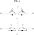
- FIG. 4(a) to (b) is diagram showing a circuit configuration example when first switch S1 includes two N-channel MOSFETs.
- FIG. 4(a) shows an example in which source terminals of two N-channel MOSFETs are connected to each other to form a bidirectional switch. In this case, since anodes of two body diodes in series face each other, a current is prevented from flowing through the body diodes between both ends of the bidirectional switch.
- FIG. 4(b) shows an example in which drain terminals of two N-channel MOSFETs are connected to each other to form a bidirectional switch.
- a current is prevented from flowing through the body diodes between both ends of the bidirectional switch.
- FIG. 5 is a diagram showing a circuit configuration example when the bidirectional switch shown in the configuration example of FIG. 4(a) is used for the switch of power storage system 1 according to the exemplary embodiment.
- the bidirectional switch shown in the configuration example of FIG. 4(a) is used for each of first switch S1, fourth switch S4, fifth switch S5, eighth switch S8, ninth switch S9, first clamp switch Sc1, second clamp switch Sc2, third clamp switch Sc3, and fourth clamp switch Sc4.
- FIG. 7(a) and (b) is diagram in which switches whose on or off states do not change during energy transfer between two cells are omitted in the circuit configuration example of power storage system 1 shown in FIG. 6(a) and (b) .
- FIG. 7(a) is a diagram in which a switch whose on or off state does not change during energy transfer between first cell C1 and second cell C2 is omitted.
- fourth switch S4 and fourth clamp switch Sc4 are drawn as simple connection since the fourth switch and the fourth clamp switch are constantly in the on state
- third clamp switch Sc3 is drawn as connection itself omitted since the third clamp switch is constantly in the off state.
- FIG. 7(b) is a diagram in which a switch whose on or off state does not change during energy transfer between first cell C1 and fourth cell C4 is omitted.
- first switch S1, fourth switch S4, and second clamp switch Sc2 are turned on, and eighth switch S8, ninth switch S9, and first clamp switch Sc1 are turned off.
- eighth switch S8, ninth switch S9, and first clamp switch Sc1 are turned off.
- first clamp switch Sc1 is turned on.
- FIG. 8(a) and (b) is diagram showing a circuit configuration example of power storage system 1 in which the discharge path and the charge path are formed when energy is transferred from the cell to be discharged to the cell to be charged in an organized manner for unified description.
- eight switching elements Q1 to Q8 are used.
- a first switching element group in which first switching element Q1 having first body diode D1 and second switching element Q2 having second body diode D2 are connected in series as a pair in opposite directions is connected to a positive-electrode terminal of upper cell Ca.
- a second switching element group in which third switching element Q3 having third body diode D3 and fourth switching element Q4 having fourth body diode D4 are connected in series as a pair in opposite directions is connected to a negative-electrode terminal of lower cell Cb.
- a negative-electrode terminal of upper cell Ca and a positive-electrode terminal of lower cell Cb are connected to the first end of inductor L1.
- a third switching element group in which fifth switching element Q5 having fifth body diode D5 and sixth switching element Q6 having sixth body diode D6 are connected in series as a pair in opposite directions is connected between both the ends of inductor L1.
- a fourth switching element group in which seventh switching element Q7 having seventh body diode D7 and eighth switching element Q8 having eighth body diode D8 are connected in series as a pair in opposite directions are connected between the second end of inductor L1 and a node between the first switching element group and the second switching element group.
- the first switching element group including first switching element Q1 and second switching element Q2 corresponds to first switch S1 in FIG. 7(a) .
- the second switching element group including third switching element Q3 and fourth switching element Q4 corresponds to fifth switch S5 in FIG. 7(a) .
- the third switching element group including fifth switching element Q5 and sixth switching element Q6 corresponds to second clamp switch Sc2 in FIG. 7(a) .
- the fourth switching element group including seventh switching element Q7 and eighth switching element Q8 corresponds to first clamp switch Sc1 in FIG. 7(a) .
- ten steps are controlled as one cycle.
- FIG. 8(b) In the circuit configuration example of power storage system 1 shown in FIG. 8(b) , eight switching elements Q1 to Q8 are used.
- the circuit configuration example shown in FIG. 8(b) is different from the circuit configuration example shown in FIG. 8(a) in that positions of a parallel circuit of inductor L1 and the third switching element group (fifth switching element Q5 and sixth switching element Q6) and the fourth switching element group (seventh switching element Q7 and eighth switching element Q8) are switched.
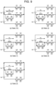
- FIG. 9(a) to (e) and FIG. 10(a) to (e) are two diagrams showing a circuit state in the control of all the ten steps according to a comparative example of power storage system 1 shown in FIG. 8(a) in correspondence with current IL of inductor L1 (state transition of ten steps in total).
- FIG. 11 is a diagram showing a switching pattern of eight switching elements Q1 to Q8, a time transition of end-to-end voltage VL of inductor L1, and current IL of inductor L1 in the control according to the comparative example of power storage system 1 shown in FIG. 8(a) .
- current IL of inductor L1 an arrow direction shown in FIG. 9(a) is represented as positive, and an opposite direction of the arrow is represented as negative.
- controller 13 controls first switching element Q1, second switching element Q2, fifth switching element Q5, seventh switching element Q7, and eighth switching element Q8 to an on state, and controls third switching element Q3, fourth switching element Q4, and sixth switching element Q6 to an off state.
- fifth switching element Q5 is controlled to an on state is in preparation for a next clamp period.
- controller 13 maintains the switching pattern of state (1).
- a discharge current flows from upper cell Ca to inductor L1.
- controller 13 turns off first switching element Q1, second switching element Q2, seventh switching element Q7, and eighth switching element Q8.
- a current flows through a clamp path formed by inductor L1 -> fifth switching element Q5 -> sixth body diode D6 -> inductor L1.
- controller 13 turns off fifth switching element Q5, and turns on third switching element Q3 and eighth switching element Q8 in preparation for a next charge period.
- a current flows through a clamp path formed by inductor L1 -> fifth switching element Q5 -> sixth switching element Q6 -> inductor L1.
- State (3) is provided for smooth and safe transition from the discharge state to the clamp state.
- an external short circuit may occur in upper cell Ca or breakdown in withstand voltage may occur in first switching element Q1 or eighth switching element Q8 due to a shift in switching timing.
- controller 13 turns off fifth switching element Q5 and sixth switching element Q6.
- state (5) a charge current flows through a path formed by inductor L1 -> lower cell Cb -> third switching element Q3 -> fourth body diode D4 -> eighth switching element Q8 -> seventh body diode D7 -> inductor L1.
- controller 13 turns on fourth switching element Q4 and seventh switching element Q7.
- state (6) a charge current flows through a path formed by inductor L1 -> lower cell Cb -> third switching element Q3 -> fourth switching element Q4 -> eighth switching element Q8 -> seventh switching element Q7 -> inductor L1.
- the state is switched from state (5) to state (6) in order to reduce the energy loss.
- State (5) is provided for smooth and safe transition from the clamp state to the charge state. For example, when the turning-off of fifth switching element Q5 and sixth switching element Q6 and the turning-on of third switching element Q3, fourth switching element Q4, seventh switching element Q7, and eighth switching element Q8 are simultaneously executed, an external short circuit may occur in lower cell Cb or breakdown in withstand voltage may occur in third switching element Q3 or eighth switching element Q8 due to a shift in switching timing. On the other hand, in state (5), since fourth body diode D4 and seventh body diode D7 are electrically connected, it is possible to prevent the external short circuit of the cell or the breakdown in withstand voltage of the switching element.
- controller 13 turns on sixth switching element Q6 in preparation for a next clamp period.
- controller 13 turns off third switching element Q3, fourth switching element Q4, seventh switching element Q7, and eighth switching element Q8.
- a current flows through a clamp path formed by inductor L1 -> sixth switching element Q6 -> fifth body diode D5 -> inductor L1.
- controller 13 turns on fifth switching element Q5, and turns on second switching element Q2 and seventh switching element Q7 in preparation for a next charge period.
- a current flows through a clamp path formed by inductor L1 -> fifth switching element Q5 -> sixth switching element Q6 -> inductor L1.
- State (8) is provided for smooth and safe transition from the discharge state to the clamp state. For example, when the turning-on of fifth switching element Q5 and sixth switching element Q6 and the turning-off of third switching element Q3, fourth switching element Q4, seventh switching element Q7, and eighth switching element Q8 are simultaneously executed, an external short circuit may occur in lower cell Cb or breakdown in withstand voltage may occur in fourth switching element Q4 or seventh switching element Q7 due to a shift in switching timing. On the other hand, in state (8), since sixth body diode D6 is electrically connected, it is possible to prevent the external short circuit of the cell or the breakdown in withstand voltage of the switching element.
- controller 13 turns off fifth switching element Q5 and sixth switching element Q6.
- a charge current flows through a path formed by inductor L1 -> seventh switching element Q7 -> eighth body diode D8 -> second switching element Q2 -> first body diode D1 -> upper cell Ca -> inductor L1.
- controller 13 turns on second switching element Q2 and seventh switching element Q7, and turns on fifth switching element Q5 in preparation for a next clamp period.
- a charge current flows through a path formed by inductor L1 -> seventh switching element Q7 -> eighth switching element Q8 -> second switching element Q2 -> first switching element Q1 -> upper cell Ca -> inductor L1. Comparing the path shown in FIG. 9(a) with the path shown in FIG.
- state (10) is switched to state (1) in order to reduce the energy loss.
- State (10) is provided for smooth and safe transition from the clamp state to the charged state.
- an external short circuit may occur in upper cell Ca or breakdown in withstand voltage may occur in first switching element Q1 or eighth switching element Q8 due to a shift in switching timing.
- state (10) since first body diode D1 and eighth body diode D8 are electrically connected, it is possible to prevent the external short circuit of the cell or the breakdown in withstand voltage of the switching element.
- current change ⁇ IL of inductor L1 in each state is as follows.
- L is an inductance
- (tn - t(n - 1)) is a time to stay in an n-th state.
- the states are drawn at equal intervals for the sake of convenience, but times of the states can be arbitrarily set.
- the clamp periods (states (3), (4), (8), and (9)) may be set shorter than the other periods (states (1), (2), (5), (6), (7), and (10)).
- the period in which the current flows through the body diode may be set shorter than the period in which the current does not flow through the body diode.
- the period of state (3) may be set shorter than the period of state (4). In this case, the loss caused by the current passing through the body diode can be further reduced.
- the MOSFET used for the switching element is an element of which the turning-on or -off is controlled by a gate voltage, and when drain-source voltage Vds changes steeply (when dV/dt increases), a current flows through a junction capacity between the drain and the gate. This current may turn on a parasitic NPN transistor between the drain and the source of the MOSFET, the breakdown of the element of the MOSFET may be caused.
- Noise generated by the spike voltage may invert high or low of the drive signal supplied from controller 13 to the gates of switching elements Q1 to Q8 and may cause equalizing circuit 10 to malfunction.
- a method for suppressing the spike voltage will be described.
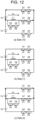
- FIG. 12(a) to (c) is diagram showing a circuit state in the control according to the exemplary embodiment of power storage system 1 shown in FIG. 8(a) in correspondence with current IL of inductor L1.
- FIG. 13 is a diagram showing a switching pattern of eight switching elements Q1 to Q8 in which FIG. 9(a) to (c) is replaced with FIG. 12(a) to (c) in a switching order of ten steps shown in FIGS. 9 and 10 , a time transition of end-to-end voltage VL of inductor L1, and current IL of inductor L1 in the control according to the exemplary embodiment of power storage system 1 shown in FIG. 8(a) .
- a difference between FIG. 9(a) to (c) and FIG. 12(a) to (c) is only a difference in the state of fifth switching element Q5 in FIGS. 9(b) and 12(b) .
- controller 13 controls first switching element Q1, second switching element Q2, seventh switching element Q7, and eighth switching element Q8 to an on state, and controls third switching element Q3, fourth switching element Q4, fifth switching element Q5, and sixth switching element Q6 to an off state.
- controller 13 turns on fifth switching element Q5 in preparation for a next clamp period.
- Other states (3) to (10) according to the exemplary embodiment are similar to states (3) to (10) according to the comparative example shown in FIGS. 9(d) to (e) , 10(a) to (e) , and 9(a) .
- a timing at which fifth switching element Q5 is turned on is delayed as preparation for a next clamp period.
- the spike voltage is not generated.
- end-to-end voltage VL of inductor L1 shown in FIG. 13 is obtained by rewriting an actual waveform obtained by an experiment into a schematic waveform, it is confirmed by an experiment that the spike shown in FIG. 11 does not occur when the state is switched from state (10) to state (1).
- the timing at which fifth switching element Q5 constituting one of the bidirectional switch used as the clamp switch is turned on is delayed as the preparation for the next clamp period, and thus, the occurrence of the unintended spike can be suppressed. Accordingly, it is possible to achieve highly reliable and safe equalizing circuit 10.
- FIG. 6(a) and (b) corresponds to the configurations of the first wiring switch and the second wiring switch of cell selection circuit 11 of power storage system 1 shown in FIG. 1 , and first clamp switch Sc1 to fourth clamp switch Sc4 of energy retaining circuit 12, and each switch of the first wiring switch, the second wiring switch, and first clamp switch Sc1 to fourth clamp switch Sc4 includes two switching elements.
- the paths (discharge path and charge path) through which energy is transferred between the selected cell and inductor L1 are formed by a total of four switches including one predetermined first wiring switch, one predetermined second wiring switch, and two predetermined clamp switches among first clamp switch Sc1 to fourth clamp switch Sc4, that is, eight switching elements, in both the discharge path and the charge path.
- the clamp path for retaining the energy stored in inductor L1 is formed by two predetermined clamp switches of first clamp switch Sc1 to fourth clamp switch Sc4, that is, four switching elements.
- a total of eight switching elements including two pairs of four switching elements present at positions where four clamp switches cross each other and one pair of two switching elements constituting the first wiring switch and the second wiring switch among the eight switching elements are controlled to the on state.
- a total of eight switching elements including two pairs of four switching elements constituting the clamp switch and one pair of two switching elements constituting the first wiring switch and the second wiring switch among the eight switching elements are controlled to an on state.
- two pairs of four switching elements among eight switching elements in the four clamp switches are controlled to an on state.
- controller 13 switches the states in the order of a first clamp state (in the above exemplary embodiment, states (3) and (8)) where the clamp current flows through the body diode of the switching element by turning off at least one switching element among the four switching elements forming the clamp path and a second clamp state (in the above exemplary embodiment, states (4) and (9)) where the switching element in the off state is turned on and all the four switching elements are turned on.
- a first clamp state in the above exemplary embodiment, states (3) and (8)
- a second clamp state in the above exemplary embodiment, states (4) and (9)
- two switching elements having body diodes in the same direction among the four switching elements forming the clamp path may be turned off. In this case, the loss increases, but safety is further improved.
- controller 13 switches the states in the order of a first charge state (in the above exemplary embodiment, states (5) and (10)) where the charge current flows through the body diode of the switching element by turning off at least one switching element among the eight switching elements forming the charge path and a second charge state (in the above exemplary embodiment, states (6) and (1)) where the switching element in the off state is turned on and all the eight switching elements are turned on.
- a first charge state in the above exemplary embodiment, states (5) and (10)
- a second charge state in the above exemplary embodiment, states (6) and (1)
- controller 13 turns off two or four switching elements among the four switching elements forming the clamp path.
- the pair of two switching elements (fifth switching element Q5 and sixth switching element Q6) is turned off, but all the four switching elements forming the clamp path may be turned off.
- controller 13 forms the clamp path in the first clamp state by turning on half of the turned-off two or four switching elements.
- the timing at which the state is switched from state (1) to state (2) is adopted as the timing delayed from the timing at which the state is switched from the first charge state to the second charge state (state (10)) and a timing before the state is switched to the next first clamp state (state (3)).
- a timing in the middle of state (1) may be adopted, or a timing in the middle of state (2) may be adopted.
- a semiconductor switching element such as an insulated gate bipolar transistor (IGBT) in which a parasitic diode is not formed may be used.
- IGBT insulated gate bipolar transistor
- an external diode is connected in parallel to the semiconductor switching element instead of the parasitic diode.
- Vf forward drop voltage
- the equalizing circuit according to the exemplary embodiment can be used to equalize a plurality of modules connected in series.
- the "cell” in the present specification may be appropriately read as a "module”.
- FIG. 14 is a diagram showing a configuration of a power storage system according to another exemplary embodiment.
- FIG. 14 shows an exemplary embodiment of a power storage system including an equalizing circuit that executes an equalizing process among a plurality of modules connected in series.
- each of the plurality of modules includes a cell equalizing circuit and a power storage in which a plurality of cells are connected in series, as in power storage system 1 shown in FIG. 1 .
- First module M1 includes cell equalizing circuit 10A and power storage 20A
- second module M2 includes cell equalizing circuit 10B and power storage 20B
- third module M3 includes cell equalizing circuit 10C and power storage 20C
- fourth module M4 includes cell equalizing circuit 10D and power storage 20D.
- Energy retaining circuit 12 (also referred to as a clamper circuit) includes inductor L1 and clamp switch Sc.
- Clamp switch Sc is a switch for electrically connecting both ends of inductor L1 in energy retaining circuit 12.
- Energy retaining circuit 12 can form a closed loop including inductor L1 in a state where cell selection circuit 11 does not select any cell. That is, when clamp switch Sc is controlled to an on state, a closed loop including inductor L1 and clamp switch Sc, that is, a clamp path is formed.
- paths (discharge path and charge path) through which energy is transferred between the selected cell and inductor L1 are formed by one predetermined first wiring switch and one predetermined second wiring switch.
Landscapes
- Engineering & Computer Science (AREA)
- Chemical & Material Sciences (AREA)
- Chemical Kinetics & Catalysis (AREA)
- Electrochemistry (AREA)
- General Chemical & Material Sciences (AREA)
- Manufacturing & Machinery (AREA)
- Power Engineering (AREA)
- Microelectronics & Electronic Packaging (AREA)
- Charge And Discharge Circuits For Batteries Or The Like (AREA)
- Secondary Cells (AREA)
Applications Claiming Priority (2)
| Application Number | Priority Date | Filing Date | Title |
|---|---|---|---|
| JP2019097418 | 2019-05-24 | ||
| PCT/JP2020/017888 WO2020241144A1 (ja) | 2019-05-24 | 2020-04-27 | エネルギ移動回路、及び蓄電システム |
Publications (3)
| Publication Number | Publication Date |
|---|---|
| EP3979391A1 EP3979391A1 (en) | 2022-04-06 |
| EP3979391A4 EP3979391A4 (en) | 2022-08-03 |
| EP3979391B1 true EP3979391B1 (en) | 2025-07-02 |
Family
ID=73554007
Family Applications (1)
| Application Number | Title | Priority Date | Filing Date |
|---|---|---|---|
| EP20813002.1A Active EP3979391B1 (en) | 2019-05-24 | 2020-04-27 | Energy transfer circuit and power storage system |
Country Status (5)
| Country | Link |
|---|---|
| US (1) | US12051921B2 (https=) |
| EP (1) | EP3979391B1 (https=) |
| JP (1) | JP7474994B2 (https=) |
| CN (1) | CN113875068B (https=) |
| WO (1) | WO2020241144A1 (https=) |
Families Citing this family (3)
| Publication number | Priority date | Publication date | Assignee | Title |
|---|---|---|---|---|
| CN112956101B (zh) * | 2018-11-02 | 2024-08-13 | 松下知识产权经营株式会社 | 能量移动电路以及蓄电系统 |
| US11577624B2 (en) * | 2019-06-05 | 2023-02-14 | GM Global Technology Operations LLC | Low voltage battery SOC confirmation and cell balancing |
| US12278508B2 (en) * | 2019-06-17 | 2025-04-15 | Renesas Electronics America Inc. | Single inductor multiple output charger for multiple battery applications |
Family Cites Families (36)
| Publication number | Priority date | Publication date | Assignee | Title |
|---|---|---|---|---|
| CN2054585U (zh) * | 1988-12-02 | 1990-03-14 | 哈尔滨船舶工程学院 | 动态功率因数补偿装置 |
| JP3328656B2 (ja) | 1994-05-25 | 2002-09-30 | 株式会社岡村研究所 | 電池の充電制御装置及び方法 |
| US6150795A (en) * | 1999-11-05 | 2000-11-21 | Power Designers, Llc | Modular battery charge equalizers and method of control |
| JP4999353B2 (ja) * | 2006-04-26 | 2012-08-15 | パナソニック株式会社 | 蓄電装置、携帯機器及び電動車両 |
| JP2008228492A (ja) * | 2007-03-14 | 2008-09-25 | Sanyo Electric Co Ltd | リチウムイオン二次電池の充電方法 |
| JP2009159726A (ja) * | 2007-12-26 | 2009-07-16 | Honda Motor Co Ltd | 放電制御装置 |
| KR101077154B1 (ko) * | 2008-04-22 | 2011-10-27 | 한국과학기술원 | 직렬연결 배터리 스트링을 위한 2단 전하 균일 방법 및장치 |
| DE102009016759A1 (de) | 2009-04-07 | 2010-10-21 | Austriamicrosystems Ag | Ladungsausgleichsschaltung für einen Energiespeicherblock und Verfahren zum Ladungsausgleich |
| JP5440400B2 (ja) * | 2010-06-03 | 2014-03-12 | 新神戸電機株式会社 | 電源装置 |
| WO2012042401A2 (en) * | 2010-09-29 | 2012-04-05 | Sendyne Corp. | Charge balancing system |
| CN107946536A (zh) * | 2010-11-29 | 2018-04-20 | 马丁·克布勒 | 起动器锂电池和用于该锂电池的固态开关 |
| CN103493331B (zh) * | 2011-04-19 | 2016-06-08 | 新电元工业株式会社 | 单元平衡电路以及单元平衡装置 |
| US9203121B2 (en) * | 2011-10-12 | 2015-12-01 | Texas Instruments Incorporated | Inductor-based active balancing for batteries and other power supplies |
| JP6116943B2 (ja) * | 2012-03-16 | 2017-04-19 | 矢崎総業株式会社 | 均等化装置 |
| CN103066665A (zh) * | 2013-01-18 | 2013-04-24 | 同济大学 | 一种动力锂离子电池模块的主动均衡电路及其均衡方法 |
| KR101450717B1 (ko) * | 2013-01-18 | 2014-10-16 | 포항공과대학교 산학협력단 | 엘씨 직렬공진을 이용한 배터리셀 밸런싱 회로 |
| KR102176586B1 (ko) * | 2013-02-27 | 2020-11-09 | 삼성전자주식회사 | 배터리에 포함된 셀들의 밸런싱을 수행하는 밸런싱 장치 및 배터리 모듈 |
| US10263434B2 (en) * | 2013-03-29 | 2019-04-16 | Nec Corporation | Charge and discharge device, charge and discharge control method, and program |
| US9203246B2 (en) * | 2013-05-16 | 2015-12-01 | Postech Academy-Industry Foundation | Balancing control circuit for battery cell module using LC series resonant circuit |
| KR101483517B1 (ko) * | 2013-08-21 | 2015-01-19 | 재단법인 포항산업과학연구원 | Dc 전력 계통용 강압형 배터리 충방전 제어 장치 |
| JP6390959B2 (ja) * | 2013-11-15 | 2018-09-19 | パナソニックIpマネジメント株式会社 | 駆動装置、電力変換装置 |
| JP6205247B2 (ja) * | 2013-11-18 | 2017-09-27 | Fdk株式会社 | バランス補正装置及び蓄電装置 |
| JP6107836B2 (ja) * | 2015-01-07 | 2017-04-05 | トヨタ自動車株式会社 | 電池監視装置 |
| CN105871022B (zh) * | 2016-05-13 | 2018-05-22 | 钛白金科技(深圳)有限公司 | 一种电池组主动均衡电路及方法 |
| JP6610453B2 (ja) * | 2016-07-06 | 2019-11-27 | 株式会社デンソー | 電源制御装置、及び電源システム |
| KR101717077B1 (ko) * | 2016-07-15 | 2017-03-16 | 포항공과대학교 산학협력단 | 단일 인덕터를 이용한 배터리셀 밸런싱 회로 |
| EP3553928B1 (en) * | 2016-12-12 | 2021-02-03 | Panasonic Intellectual Property Management Co., Ltd. | Snubber circuit and power conversion system using same |
| CN106532852B (zh) * | 2016-12-16 | 2023-06-20 | 华南理工大学 | 基于lc串联储能的电池组均衡电路 |
| WO2018134827A1 (en) * | 2017-01-23 | 2018-07-26 | B.G. Negev Technologies And Applications Ltd., At Ben-Gurion University | System for balancing a series of cells |
| CN108110817A (zh) * | 2017-08-15 | 2018-06-01 | 哈尔滨工业大学 | 串联储能电源多路径均衡装置及方法 |
| US10833512B2 (en) * | 2017-11-14 | 2020-11-10 | Neapco Intellectual Property Holdings, Llc | Cell balancing with local sensing and switching |
| US11894702B2 (en) * | 2018-09-06 | 2024-02-06 | Panasonic Intellectual Property Management Co., Ltd. | Energy transfer circuit and power storage system |
| JP7328750B2 (ja) * | 2018-10-31 | 2023-08-17 | 株式会社豊田中央研究所 | 電源装置 |
| US10658856B1 (en) * | 2018-11-02 | 2020-05-19 | Monolithic Power Systems, Inc. | Battery pack and discharge method for limiting an excessive discharge current |
| WO2020188567A1 (en) | 2019-03-18 | 2020-09-24 | Infimer Technologies Ltd. | Polymeric material derived from waste material |
| CN110649336B (zh) * | 2019-10-23 | 2024-03-08 | 西南交通大学 | 一种具有完备均衡支路的电压均衡电路及控制方法 |
-
2020
- 2020-04-27 JP JP2021522722A patent/JP7474994B2/ja active Active
- 2020-04-27 CN CN202080037345.8A patent/CN113875068B/zh active Active
- 2020-04-27 EP EP20813002.1A patent/EP3979391B1/en active Active
- 2020-04-27 WO PCT/JP2020/017888 patent/WO2020241144A1/ja not_active Ceased
- 2020-04-27 US US17/611,211 patent/US12051921B2/en active Active
Also Published As
| Publication number | Publication date |
|---|---|
| JPWO2020241144A1 (https=) | 2020-12-03 |
| CN113875068A (zh) | 2021-12-31 |
| CN113875068B (zh) | 2024-11-29 |
| EP3979391A1 (en) | 2022-04-06 |
| US12051921B2 (en) | 2024-07-30 |
| US20220216703A1 (en) | 2022-07-07 |
| JP7474994B2 (ja) | 2024-04-26 |
| EP3979391A4 (en) | 2022-08-03 |
| WO2020241144A1 (ja) | 2020-12-03 |
Similar Documents
| Publication | Publication Date | Title |
|---|---|---|
| US11437828B2 (en) | Equalization circuit and power storage system | |
| US8692508B2 (en) | Battery voltage monitoring device | |
| US11962172B2 (en) | Power supply system and management device | |
| EP2804780B1 (en) | Electric vehicle running control system | |
| US12240338B2 (en) | Power supply system including an electrical machine with its neutral point connected to a power supply unit | |
| EP3979391B1 (en) | Energy transfer circuit and power storage system | |
| CN102438854A (zh) | 可电驱动的机动车 | |
| JP5794982B2 (ja) | 電源装置及び充電回路 | |
| US11894702B2 (en) | Energy transfer circuit and power storage system | |
| US12088129B2 (en) | Energy transfer circuit and power storage system | |
| US9045046B2 (en) | Electrical charging system | |
| EP4037124B1 (en) | Energy transfer circuit, and electricity storage system | |
| CN209982099U (zh) | 一种电池组热插拔保护电路 | |
| HK1158375B (en) | Battery heating circuit | |
| HK1158375A1 (en) | Battery heating circuit |
Legal Events
| Date | Code | Title | Description |
|---|---|---|---|
| STAA | Information on the status of an ep patent application or granted ep patent |
Free format text: STATUS: THE INTERNATIONAL PUBLICATION HAS BEEN MADE |
|
| PUAI | Public reference made under article 153(3) epc to a published international application that has entered the european phase |
Free format text: ORIGINAL CODE: 0009012 |
|
| STAA | Information on the status of an ep patent application or granted ep patent |
Free format text: STATUS: REQUEST FOR EXAMINATION WAS MADE |
|
| 17P | Request for examination filed |
Effective date: 20211126 |
|
| AK | Designated contracting states |
Kind code of ref document: A1 Designated state(s): AL AT BE BG CH CY CZ DE DK EE ES FI FR GB GR HR HU IE IS IT LI LT LU LV MC MK MT NL NO PL PT RO RS SE SI SK SM TR |
|
| A4 | Supplementary search report drawn up and despatched |
Effective date: 20220706 |
|
| RIC1 | Information provided on ipc code assigned before grant |
Ipc: H01M 50/51 20210101ALI20220630BHEP Ipc: H01M 50/204 20210101ALI20220630BHEP Ipc: H01M 10/46 20060101ALI20220630BHEP Ipc: H01M 10/42 20060101ALI20220630BHEP Ipc: H02J 7/00 20060101ALI20220630BHEP Ipc: H02J 7/02 20160101ALI20220630BHEP Ipc: H01M 10/48 20060101ALI20220630BHEP Ipc: H01M 10/44 20060101AFI20220630BHEP |
|
| DAV | Request for validation of the european patent (deleted) | ||
| DAX | Request for extension of the european patent (deleted) | ||
| GRAP | Despatch of communication of intention to grant a patent |
Free format text: ORIGINAL CODE: EPIDOSNIGR1 |
|
| STAA | Information on the status of an ep patent application or granted ep patent |
Free format text: STATUS: GRANT OF PATENT IS INTENDED |
|
| INTG | Intention to grant announced |
Effective date: 20250401 |
|
| GRAS | Grant fee paid |
Free format text: ORIGINAL CODE: EPIDOSNIGR3 |
|
| GRAA | (expected) grant |
Free format text: ORIGINAL CODE: 0009210 |
|
| STAA | Information on the status of an ep patent application or granted ep patent |
Free format text: STATUS: THE PATENT HAS BEEN GRANTED |
|
| AK | Designated contracting states |
Kind code of ref document: B1 Designated state(s): AL AT BE BG CH CY CZ DE DK EE ES FI FR GB GR HR HU IE IS IT LI LT LU LV MC MK MT NL NO PL PT RO RS SE SI SK SM TR |
|
| REG | Reference to a national code |
Ref country code: GB Ref legal event code: FG4D |
|
| REG | Reference to a national code |
Ref country code: CH Ref legal event code: EP |
|
| REG | Reference to a national code |
Ref country code: DE Ref legal event code: R096 Ref document number: 602020053918 Country of ref document: DE |
|
| REG | Reference to a national code |
Ref country code: IE Ref legal event code: FG4D |
|
| REG | Reference to a national code |
Ref country code: NL Ref legal event code: MP Effective date: 20250702 |
|
| PG25 | Lapsed in a contracting state [announced via postgrant information from national office to epo] |
Ref country code: PT Free format text: LAPSE BECAUSE OF FAILURE TO SUBMIT A TRANSLATION OF THE DESCRIPTION OR TO PAY THE FEE WITHIN THE PRESCRIBED TIME-LIMIT Effective date: 20251103 |
|
| PG25 | Lapsed in a contracting state [announced via postgrant information from national office to epo] |
Ref country code: NL Free format text: LAPSE BECAUSE OF FAILURE TO SUBMIT A TRANSLATION OF THE DESCRIPTION OR TO PAY THE FEE WITHIN THE PRESCRIBED TIME-LIMIT Effective date: 20250702 |
|
| REG | Reference to a national code |
Ref country code: AT Ref legal event code: MK05 Ref document number: 1810324 Country of ref document: AT Kind code of ref document: T Effective date: 20250702 |
|
| PG25 | Lapsed in a contracting state [announced via postgrant information from national office to epo] |
Ref country code: IS Free format text: LAPSE BECAUSE OF FAILURE TO SUBMIT A TRANSLATION OF THE DESCRIPTION OR TO PAY THE FEE WITHIN THE PRESCRIBED TIME-LIMIT Effective date: 20251102 |
|
| PG25 | Lapsed in a contracting state [announced via postgrant information from national office to epo] |
Ref country code: NO Free format text: LAPSE BECAUSE OF FAILURE TO SUBMIT A TRANSLATION OF THE DESCRIPTION OR TO PAY THE FEE WITHIN THE PRESCRIBED TIME-LIMIT Effective date: 20251002 |
|
| REG | Reference to a national code |
Ref country code: LT Ref legal event code: MG9D |
|
| PG25 | Lapsed in a contracting state [announced via postgrant information from national office to epo] |
Ref country code: AT Free format text: LAPSE BECAUSE OF FAILURE TO SUBMIT A TRANSLATION OF THE DESCRIPTION OR TO PAY THE FEE WITHIN THE PRESCRIBED TIME-LIMIT Effective date: 20250702 |
|
| PG25 | Lapsed in a contracting state [announced via postgrant information from national office to epo] |
Ref country code: FI Free format text: LAPSE BECAUSE OF FAILURE TO SUBMIT A TRANSLATION OF THE DESCRIPTION OR TO PAY THE FEE WITHIN THE PRESCRIBED TIME-LIMIT Effective date: 20250702 |
|
| PG25 | Lapsed in a contracting state [announced via postgrant information from national office to epo] |
Ref country code: HR Free format text: LAPSE BECAUSE OF FAILURE TO SUBMIT A TRANSLATION OF THE DESCRIPTION OR TO PAY THE FEE WITHIN THE PRESCRIBED TIME-LIMIT Effective date: 20250702 |
|
| PG25 | Lapsed in a contracting state [announced via postgrant information from national office to epo] |
Ref country code: GR Free format text: LAPSE BECAUSE OF FAILURE TO SUBMIT A TRANSLATION OF THE DESCRIPTION OR TO PAY THE FEE WITHIN THE PRESCRIBED TIME-LIMIT Effective date: 20251003 |
|
| PG25 | Lapsed in a contracting state [announced via postgrant information from national office to epo] |
Ref country code: CZ Free format text: LAPSE BECAUSE OF FAILURE TO SUBMIT A TRANSLATION OF THE DESCRIPTION OR TO PAY THE FEE WITHIN THE PRESCRIBED TIME-LIMIT Effective date: 20250702 Ref country code: SE Free format text: LAPSE BECAUSE OF FAILURE TO SUBMIT A TRANSLATION OF THE DESCRIPTION OR TO PAY THE FEE WITHIN THE PRESCRIBED TIME-LIMIT Effective date: 20250702 |
|
| PG25 | Lapsed in a contracting state [announced via postgrant information from national office to epo] |
Ref country code: LV Free format text: LAPSE BECAUSE OF FAILURE TO SUBMIT A TRANSLATION OF THE DESCRIPTION OR TO PAY THE FEE WITHIN THE PRESCRIBED TIME-LIMIT Effective date: 20250702 |
|
| PG25 | Lapsed in a contracting state [announced via postgrant information from national office to epo] |
Ref country code: BG Free format text: LAPSE BECAUSE OF FAILURE TO SUBMIT A TRANSLATION OF THE DESCRIPTION OR TO PAY THE FEE WITHIN THE PRESCRIBED TIME-LIMIT Effective date: 20250702 Ref country code: PL Free format text: LAPSE BECAUSE OF FAILURE TO SUBMIT A TRANSLATION OF THE DESCRIPTION OR TO PAY THE FEE WITHIN THE PRESCRIBED TIME-LIMIT Effective date: 20250702 |
|
| PG25 | Lapsed in a contracting state [announced via postgrant information from national office to epo] |
Ref country code: RS Free format text: LAPSE BECAUSE OF FAILURE TO SUBMIT A TRANSLATION OF THE DESCRIPTION OR TO PAY THE FEE WITHIN THE PRESCRIBED TIME-LIMIT Effective date: 20251002 |
|
| PG25 | Lapsed in a contracting state [announced via postgrant information from national office to epo] |
Ref country code: ES Free format text: LAPSE BECAUSE OF FAILURE TO SUBMIT A TRANSLATION OF THE DESCRIPTION OR TO PAY THE FEE WITHIN THE PRESCRIBED TIME-LIMIT Effective date: 20250702 |
|
| PG25 | Lapsed in a contracting state [announced via postgrant information from national office to epo] |
Ref country code: SM Free format text: LAPSE BECAUSE OF FAILURE TO SUBMIT A TRANSLATION OF THE DESCRIPTION OR TO PAY THE FEE WITHIN THE PRESCRIBED TIME-LIMIT Effective date: 20250702 |
|
| PG25 | Lapsed in a contracting state [announced via postgrant information from national office to epo] |
Ref country code: DK Free format text: LAPSE BECAUSE OF FAILURE TO SUBMIT A TRANSLATION OF THE DESCRIPTION OR TO PAY THE FEE WITHIN THE PRESCRIBED TIME-LIMIT Effective date: 20250702 |
|
| PG25 | Lapsed in a contracting state [announced via postgrant information from national office to epo] |
Ref country code: IT Free format text: LAPSE BECAUSE OF FAILURE TO SUBMIT A TRANSLATION OF THE DESCRIPTION OR TO PAY THE FEE WITHIN THE PRESCRIBED TIME-LIMIT Effective date: 20250702 |
|
| PG25 | Lapsed in a contracting state [announced via postgrant information from national office to epo] |
Ref country code: EE Free format text: LAPSE BECAUSE OF FAILURE TO SUBMIT A TRANSLATION OF THE DESCRIPTION OR TO PAY THE FEE WITHIN THE PRESCRIBED TIME-LIMIT Effective date: 20250702 Ref country code: SK Free format text: LAPSE BECAUSE OF FAILURE TO SUBMIT A TRANSLATION OF THE DESCRIPTION OR TO PAY THE FEE WITHIN THE PRESCRIBED TIME-LIMIT Effective date: 20250702 |