EP3973335B1 - Mehrschichtige optische folie - Google Patents
Mehrschichtige optische folie Download PDFInfo
- Publication number
- EP3973335B1 EP3973335B1 EP20810705.2A EP20810705A EP3973335B1 EP 3973335 B1 EP3973335 B1 EP 3973335B1 EP 20810705 A EP20810705 A EP 20810705A EP 3973335 B1 EP3973335 B1 EP 3973335B1
- Authority
- EP
- European Patent Office
- Prior art keywords
- layers
- polymeric layers
- optical film
- thickness
- polymeric
- Prior art date
- Legal status (The legal status is an assumption and is not a legal conclusion. Google has not performed a legal analysis and makes no representation as to the accuracy of the status listed.)
- Active
Links
Images


Classifications
-
- G—PHYSICS
- G02—OPTICS
- G02B—OPTICAL ELEMENTS, SYSTEMS OR APPARATUS
- G02B5/00—Optical elements other than lenses
- G02B5/20—Filters
- G02B5/28—Interference filters
- G02B5/285—Interference filters comprising deposited thin solid films
- G02B5/287—Interference filters comprising deposited thin solid films comprising at least one layer of organic material
-
- B—PERFORMING OPERATIONS; TRANSPORTING
- B32—LAYERED PRODUCTS
- B32B—LAYERED PRODUCTS, i.e. PRODUCTS BUILT-UP OF STRATA OF FLAT OR NON-FLAT, e.g. CELLULAR OR HONEYCOMB, FORM
- B32B7/00—Layered products characterised by the relation between layers; Layered products characterised by the relative orientation of features between layers, or by the relative values of a measurable parameter between layers, i.e. products comprising layers having different physical, chemical or physicochemical properties; Layered products characterised by the interconnection of layers
- B32B7/02—Physical, chemical or physicochemical properties
-
- G—PHYSICS
- G02—OPTICS
- G02B—OPTICAL ELEMENTS, SYSTEMS OR APPARATUS
- G02B5/00—Optical elements other than lenses
- G02B5/30—Polarising elements
- G02B5/3025—Polarisers, i.e. arrangements capable of producing a definite output polarisation state from an unpolarised input state
- G02B5/3033—Polarisers, i.e. arrangements capable of producing a definite output polarisation state from an unpolarised input state in the form of a thin sheet or foil, e.g. Polaroid
- G02B5/3041—Polarisers, i.e. arrangements capable of producing a definite output polarisation state from an unpolarised input state in the form of a thin sheet or foil, e.g. Polaroid comprising multiple thin layers, e.g. multilayer stacks
- G02B5/305—Polarisers, i.e. arrangements capable of producing a definite output polarisation state from an unpolarised input state in the form of a thin sheet or foil, e.g. Polaroid comprising multiple thin layers, e.g. multilayer stacks including organic materials, e.g. polymeric layers
-
- G—PHYSICS
- G02—OPTICS
- G02B—OPTICAL ELEMENTS, SYSTEMS OR APPARATUS
- G02B5/00—Optical elements other than lenses
- G02B5/30—Polarising elements
- G02B5/3083—Birefringent or phase retarding elements
Definitions
- Multilayer optical films may include packets of microlayers separated by optically thick protective boundary layers.
- a multilayer optical film including a plurality of polymeric layers arranged sequentially adjacent to each other.
- a difference in thickness between spaced apart first and second polymeric layers in the plurality of polymeric layers is less than about 10%.
- Each polymeric layer disposed between the first and second polymeric layers has a thickness less than about 400 nm.
- Each layer in a group of at least three polymeric layers in the plurality of polymeric layers that are disposed between the first and second polymeric layers has a thickness greater than an average thickness of the first and second polymeric layers by about 20% to about 500%.
- the group of at least three polymeric layers includes at least one pair of immediately adjacent polymeric layers.
- a multilayer optical film including a plurality of optical repeat units arranged sequentially adjacent to each other along at least a portion of a thickness of the multilayer optical film.
- Each optical repeat unit includes at least two layers and has a corresponding bandwidth. The bandwidths of spaced apart first and second optical repeat units in the plurality of optical repeat units overlap each other. At least a pair of adjacent optical repeat units in the plurality of optical repeat units that are disposed between the first and second optical repeat units have non-overlapping bandwidths.
- No optical repeat unit disposed between the first and second optical repeat units has a thickness less than an average thickness of the first and second optical repeat units by more than about 10%.
- Each layer in the multilayer optical film disposed between the first and second optical repeat units has an average thickness less than about 400 nm.
- a multilayer optical film including a plurality of alternating layers of first and second polymeric layers arranged sequentially adjacent to each other. At least first through fourth sequentially arranged adjacent layers in the plurality of alternating layers of the first and second polymeric layers have intended average thicknesses t1 through t4, respectively.
- Each of t1 through t4 is less than about 400 nm.
- One of t2 and t3 is greater than t1, t4 and the other one of t2 and t3 by at least 5%.
- a multilayer optical film including a first multilayer stack, a second multilayer stack, and a third multilayer stack disposed therebetween.
- Each of the first, second, and third multilayer stacks includes a plurality of polymeric layers. A total number of polymeric layers in each of the first and second multilayer stacks is at least 50.
- the first and second multilayer stacks include respective first and second polymer layers immediately adjacent the third multilayer stack, where a difference in thickness between the first and second polymeric layers is less than about 10%.
- the third multilayer stack includes at least one pair of immediately adjacent polymeric layers such that each polymeric layer in the at least one pair has a thickness greater than an average thickness of the first and second polymeric layers by at least about 20%.
- the multilayer optical film is integrally formed and a minimum average peel force between first and second portions of the multilayer optical film is greater than about 0.4 N/cm, where the first and second portions include at least one polymeric layer of the first and second multilayer stacks, respectively.
- Multilayer optical films that provide desirable transmission and/or reflection properties at least partially by an arrangement of microlayers of differing refractive index, are known. Such optical films have been demonstrated, for example, by coextrusion of alternating polymer layers, casting the layers through a film die onto a chill roll, and then stretching the cast web. See, e.g., U.S. Pat. Nos. 3,610,729 (Rogers ), 4,446,305 (Rogers et al. ), 4,540,623 (Im et al. ), 5,448,404 (Schrenk et al. ), 5,882,774 (Jonza et al. ), 6,157,490 (Wheatley et al.
- polymer materials may be used predominantly or exclusively in the makeup of the individual layers. Such films are compatible with high volume manufacturing processes and can be made in large sheets and roll goods.
- the multilayer optical film can be configured to be a broadband (e.g., a visible and/or near infrared wavelength range) reflective polarizer, a broadband mirror, a notch (e.g., having relatively narrow spaced apart reflection bands) reflective polarizer, or a notch mirror, for example.
- a broadband e.g., a visible and/or near infrared wavelength range
- a broadband mirror e.g., a notch (e.g., having relatively narrow spaced apart reflection bands) reflective polarizer, or a notch mirror, for example.
- a multilayer optical film includes two or more optical stacks or optical packets of optical repeat units.
- An optical repeat unit includes two or more layers and is repeated across a stack or packet of the optical repeat units.
- An optical repeat unit has a first order reflection for a wavelength twice the optical thickness (thickness times refractive index) of the optical repeat unit.
- Each layer in a packet of optical repeat units may have a thickness less than 400 nm, or less than 300 nm, or less than 250 nm, or less than 200 nm.
- Each layer may have a thickness greater than about 5 nm or greater than about 10 nm.
- a multilayer optical film may include two packets of optical repeat units, where one packet is configured to reflect blue to green wavelengths and the other packet is configured to reflect green to red wavelengths, for example.
- One or more spacer layers may be included between the packets of optical repeat units.
- one or two optically thick too thick to substantially contribute to a first order visible (e.g., wavelengths in a range of about 400 nm to about 700 nm) or near infrared (e.g., wavelengths in a range of about 700 nm to about 2500 nm) light reflection by optical interference
- spacer layers or protective boundary layers (PBLs) have been included.
- These PBL layers are typically included to prevent flow profiles in the coextruded web of alternating polymer layers from producing optical defects in the alternating polymer layers. According to the present description, it has been found that using thinner PBLs can provide improved resistance against delamination of adjacent optical packets, but that thinner PBLs can also result in optical defects. According to some embodiments of the present description, it has been found that using a larger number of thinner PBLs provides improved delamination resistance between optical packets without resulting in optical defects. According to some embodiments, these thinner PBLs are preferably less than about 400 nm thick. In some embodiments, three or more PBL layers are included between adjacent packets of optical repeat units. In some embodiments, at least some, and in some cases, all, of these PBL layers are optical layers.
- An optical layer in this context is a layer having a thickness in a range that that the layer can significantly contribute to first order visible or near infrared light reflection by optical interference.
- the thickness profiles of the PBLs are chosen to prevent or reduce optical coherence from such reflections (e.g., different optical repeat units in the PBLs may have non-overlapping bandwidths) so that the PBLs do not substantially affect the reflectance of the multilayer optical film.
- FIG. 1 is a schematic cross-sectional view of a multilayer optical film 100.
- the optical film 100 includes a plurality of polymeric layers 102 arranged sequentially adjacent to each other.
- the percent difference in thickness of the first and second layers 111 and 112 is
- each layer in a group 120 of at least three polymeric layers in the plurality of polymeric layers 102 that are disposed between the first and second polymeric layers 111 and 112 have a thickness (e.g., t1, t2, t3) greater than an average thickness ((h1+h2)/2) of the first and second polymeric layers by at least about 50%, or at least about 100%, or at least about 150%.
- each layer in the group 120 has a thickness that is greater than the average thickness of the first and second polymeric layers by no more than about 400%, or no more than about 300%, or no more than about 250%.
- the group 120 of at least three polymeric layers has an average thickness (e.g., (t1+t2+t3)/3 in the illustrated embodiment) that is greater than the average thickness of the first and second polymeric layers 111 and 112 by about 50% to about 400%, or about 100% to about 300%, or about 150% to about 250%.
- average thickness e.g., (t1+t2+t3)/3 in the illustrated embodiment
- each layer in a multilayer optical film has a constant or approximately constant thickness.
- the thickness of the layer refers to an average (unweighted mean) thickness of the layer, unless indicated differently.
- the average thickness of a set or group of layers is the arithmetic mean of the thicknesses of the individual layers in the set or group.
- the intended average thickness of a layer is a design or nominal thickness of the layer. In some embodiments, the intended average thickness of a layer is the same or substantially the same as the average thickness of the layer.
- the group 120 of at least three polymeric layers includes at least one pair of immediately adjacent polymeric layers (e.g., 124 and 122, or 122 and 119).
- the polymeric layers in the group 120 of at least three polymeric layers are arranged sequentially adjacent to each other as schematically illustrated in FIG. 1 .
- the additional polymeric layer(s) may separate some of the polymeric layers in the group 120.
- the optical film 100 may include many more layers than schematically illustrated in FIG. 1 .
- the multilayer optical film 100 includes at least 50 layers, or at least 100 layers, or at least 200 layers. In some such embodiments or in other embodiments, the multilayer optical film 100 includes no more than 1000 layers, or no more than 800 layers.
- the polymeric layers 128 are the polymeric layers in the plurality of polymeric layers that are disposed between the first and second polymeric layers 111 and 112. In some embodiments, a total number of polymeric layers 128 in the plurality of polymeric layers that are disposed between the first and second polymeric layers 111 and 112 is at least 3, or at least 4, or at least 5. In the invention, a total number of polymeric layers 128 in the plurality of polymeric layers that are disposed between the first and second polymeric layers 111 and 112 is no more than 30, or no more than 25, or no more than 20, or no more than 15, or no more than 12, or no more than 10.
- the multilayer optical film 100 may have desired optical transmittances and reflectances for substantially normally incident light 144 (e.g., light normally incident or light incident within 30 degrees, or within 20 degrees, or within 10 degrees of normal) having a first polarization state 145 and for substantially normally incident light 146 having a second polarization state 147.
- substantially normally incident light 144 e.g., light normally incident or light incident within 30 degrees, or within 20 degrees, or within 10 degrees of normal
- substantially normally incident light 146 having a second polarization state 147.
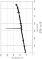
- FIG. 2A is a plot of layer thickness versus layer number for a multilayer optical film that may correspond to multilayer optical film 100.
- FIG. 2B is a portion of the plot of FIG. 2A illustrating spaced apart first and second polymeric layers 211 and 212 and a group 220 of at least three polymeric layers disposed between the first and second polymeric layers 211 and 212. Data points at integer layer numbers are shown. The lines between the data points are a guide to the eye.
- First layer 211 has a thickness of 84.3 nm
- second layer 212 a thickness of 84.4 nm
- the layers in the group 220 have thickness of 175.5 nm, 196.2 nm, 129.8 nm, and 112.3 nm, respectively.
- Each layer in the group 220 had a thickness greater than an average thickness of the first and second layers 211 and 212 by about 33% to about 133% (e.g., (112.3 nm - 84.35 nm)/84.35 nm times 100% is about 33%).
- the group 120 or 220 of at least three polymeric layers in the plurality of polymeric layers is a group of at least four polymeric layers in the plurality of polymeric layers. In some embodiments, the group of at least three polymeric layers includes less than 20 polymeric layers, or less than 15 polymeric layers, or less than 10 polymeric layers.
- each of the first and second polymeric layers 111 and 112, or 211 and 212 is disposed between the group 120 or 220 of at least three polymeric layers and at least 50 other polymeric layers in the plurality of polymeric layers.
- the groups of layers 125 and 126 schematically illustrated in FIG. 1 may each include at least 50 layers.
- each layer disposed between the first and second polymeric layers 111 and 112, or 211 and 212 has a thickness (e.g., average thickness of the layer) less than about 1 micron, or less than about 700 nm, or preferably less than about 500 nm, or more preferably less than about 400 nm, or even more preferably less than about 300 nm or less than about 250 nm.
- a thickness e.g., average thickness of the layer
- no layer disposed between the first and second polymeric layers 111 and 112, or 211 and 212 has a thickness (e.g., average thickness of the layer) that is less than the average thickness of the first and second polymeric layers by more than about 10%, or by more than about 5%.
- a thickness e.g., average thickness of the layer
- no layer disposed between the first and second polymeric layers 111 and 112, or 211 and 212 has a thickness less than about 0.9, or less than about 0.95, times the average thickness of the first and second polymeric layers.
- the multilayer optical film 100 includes a first group 140 of polymeric layers arranged sequentially adjacent to each other along at least a portion of a thickness of the multilayer optical film 100.
- the first group 140 includes at least 200 polymeric layers (fewer layers are shown in the schematic illustration of FIG. 1 ) arranged sequentially adjacent to each other along at least a portion of a thickness of the multilayer optical film 100.
- the first group 140 may correspond to a group of layers of FIG. 2A-2B including at least layer numbers 200 to 400.
- the first group 140 of polymeric layers includes the first and second polymeric layers 111 and 112 and the group 120 of at least three polymeric layers.
- Each layer in the first group 140 of at least 200 polymeric layers has a thickness (e.g., average thickness of the layer) less than about 1 micron, or less than about 700 nm, or preferably less than about 500 nm, or more preferably less than about 400 nm, or even more preferably less than about 300 nm or less than about 250 nm.
- a thickness e.g., average thickness of the layer
- a multilayer optical film 100 includes a plurality of optical repeat units (e.g., layer pairs 103, 104) arranged sequentially adjacent to each other along at least a portion of a thickness of the multilayer optical film 100.
- Each optical repeat unit includes at least two layers 103 and 104 and has a corresponding bandwidth.
- a first optical repeat unit 111, 113 may have a bandwidth W1 between left and right wavelengths ⁇ 1L and ⁇ 1R and a second optical repeat unit 112, 114 may have a bandwidth W2 between left and right wavelengths ⁇ 2L and ⁇ 2R as schematically illustrated in FIG. 3 .
- the left and right wavelengths can be understood to be the full-width at half maximum (FWHM) band edge wavelengths.
- the bandwidths of spaced apart first and second optical repeat units 111, 113 and 112, 114 in the plurality of optical repeat units overlap each other.
- ⁇ 2L is between ⁇ 1L and ⁇ 1R
- ⁇ 1R is between ⁇ 2L and ⁇ 2R.
- at least a pair of adjacent optical repeat units (e.g., 124, 122 and 119, 117) in the plurality of optical repeat units that are disposed between the first and second optical repeat units 111, 113 and 112, 114 have non-overlapping bandwidths. This is schematically illustrated in FIG.
- no optical repeat unit disposed between the first and second optical repeat units has a thickness less than an average thickness of the first and second optical repeat units by more than about 10%, or by more than about 5%.
- the thickness of an optical repeat unit is the total thickness of the at least two layers in the optical repeat unit.
- each layer in the multilayer optical film that is disposed between the first and second optical repeat units has a thickness (e.g., average thickness of the layer) less than less than about 1 micron, or less than about 700 nm, or preferably less than about 500 nm, or more preferably less than about 400 nm, or even more preferably less than about 300 nm or less than about 250 nm.
- a thickness e.g., average thickness of the layer
- the bandwidth of an optical repeat unit is the bandwidth of a first order reflection band that an infinite stack of ORU's of identical thickness would exhibit. This is readily calculated from the matrix elements of the characteristic matrix M as defined by Born and Wolf, "Principles of Optics", Edition 5, page 67.
- the optical repeat unit may include two layers or may include more than two layers.
- each optical repeat unit includes at least three layers, or at least four layers.
- FIG. 5 is a schematic cross-sectional view of an optical repeat unit 505 including two layers 503 and 504.
- each of the layers 503 and 504 have an optical thickness of a quarter of substantially a same wavelength.
- one or both of the layers 503 and 504 is replaced with two (or more) layers.
- the two (or more) layers have a combined optical thickness of a quarter of a wavelength that the optical repeat unit is configured to reflect.
- FIG. 6 is a schematic cross-sectional view of an optical repeat unit 605 including four layers 603, 607, 604, 608.
- layers 607 and 608 are tie layers included to improve bonding to adjacent layers.
- the layers 607 and 608 have a thickness in a range of about 5 nm to about 50 nm, or about 10 nm to about 30 nm, for example.
- the layers 607 and 608 have a same composition.
- each optical repeat unit 605 includes layers A (603), B (607 or 608), and C (604) arranged in an order ABCB.
- layers AB and CB have an optical thickness of a quarter of substantially a same wavelength.
- a multilayer optical film 100 includes a plurality of alternating layers of first and second polymeric layers 103 and 104 arranged sequentially adjacent to each other. At least first through fourth sequentially arranged adjacent layers (e.g., layers 124, 122, 119, and 117, respectively) in the plurality of alternating layers of the first and second polymeric layers 103 and 104 have intended average thicknesses t1 through t4, respectively, where one of t2 and t3 is greater than t1, t4 and the other one of t2 and t3 by at least 5%, or by at least 7%, or by at least 10%, or by at least 15%, or at least 20%, or at least 30%.
- one of t2 and t3 is greater than t1, t4 and the other one of t2 and t3 by about 5% to about 500%; or about 10% to about 500%; or about 20% to about 500%, or to about 400%, or to about 300%, or to about 250%.
- each of t1 through t4 is less than about 1 micron, or less than about 700 nm, or preferably less than about 500 nm, or more preferably less than about 400 nm, or even more preferably less than about 300 nm or less than about 250 nm.
- the multilayer optical film 100 is a reflective polarizer.
- FIG. 7 is a schematic plot of the transmittance of an optical film versus wavelength for substantially normally incident for first and second polarizations states 745 and 747.
- the wavelength range depicted in FIG. 7 may be at least 200 nm wide (e.g., at least from 450 nm to 650 nm, or from 400 nm to 700 nm).
- the multilayer optical film 100 has an average optical reflectance of at least 60% for a first polarization state 745 and an average optical transmittance T2 of at least 60% for an orthogonal second polarization state 747. Often, the optical absorption is negligible so that the average optical reflectance is about 100% minus T1.
- U (1/MDDR - 1) / (TDDR 1/2 - 1) with MDDR defined as the machine direction draw ratio and TDDR defined as the transverse direction draw ratio.
- the multilayer optical film 100 is a mirror film. In some embodiments, for substantially normally incident light in a wavelength range of at least 200 nm, the multilayer optical film 100 has an average optical reflectance of at least 60% for each of mutually orthogonal first and second polarization states. For example, the transmittance for the first and second polarization states may each follow the curve labeled 747 in FIG. 7 .
- the transmittance may be significantly different from the schematic illustration of FIG. 7 .
- the transmittance may vary with wavelength rather than being constant or substantially constant over a wavelength range.
- the multilayer optical film 100 is a reflective polarizer having spaced apart reflection bands.
- FIG. 8 is a schematic plot of the transmittance of an optical film versus wavelength for substantially normally incident for first and second polarizations states 845 and 847.
- the multilayer optical film 100 reflects at least 60% of the incident light having a first polarization state 845 and transmits at least 60% of the incident light having an orthogonal second polarization state 847.
- the multilayer optical film 100 transmits at least 60% of the incident light for each of the first and second polarization states 845 and 847.
- the transmittance may be significantly different from the schematic illustration of FIG. 8 .
- the transmittance or reflectance in the reflection bands near ⁇ 1 and ⁇ 2 may vary within the bands and may have more gradual band edge transitions.
- the transmittance or reflectance may be significantly different for the reflection band near ⁇ 1 and the reflection band near ⁇ 2.
- the multilayer optical films of the present description may be integrally formed.
- a first element "integrally formed" with a second element means that the first and second elements are manufactured together rather than manufactured separately and then subsequently joined. Integrally formed includes manufacturing a first element followed by manufacturing the second element on the first element.
- An optical film including a plurality of layers is integrally formed if the layers are manufactured together (e.g., combined as melt streams and then cast onto a chill roll to form a cast film which is then oriented) rather than manufactured separately and then subsequently joined.
- a multilayer optical film 100 includes a first multilayer stack (layer 111 with group of layers 124), a second multilayer stack (layer 112 with group of layers 126), and a third multilayer stack (group of layers 128) disposed therebetween.
- Each of the first, second, and third multilayer stacks include a plurality of polymeric layers.
- a total number of polymeric layers in each of the first and second multilayer stacks is at least 50, or at least 100, or at least 150, or at least 200.
- a total number of polymeric layers in the third multilayer stack is at least 3, or at least 4, or at least 5, and, in the invention, no more than 30, or no more than 25, or no more than 20, or no more than 15, or no more than 12, or no more than 10.
- each polymeric layer in the third multilayer stack has a thickness less than 400 nm, or less than 300 nm, or less than 250 nm.
- Each of the first and second multilayer stacks, and optionally the third multilayer stack may be optical stacks including a plurality of optical repeat units as described elsewhere.
- the first and second multilayer stacks include respective first and second polymer layers 111 and 112 immediately adjacent the third multilayer stack (group of layers 128).
- the third multilayer stack includes at least one pair of immediately adjacent polymeric layers (e.g., 124 and 122, or 122 and 119) such that each polymeric layer in the at least one pair has a thickness greater than an average thickness of the first and second polymeric layers by at least about 20%. In some embodiments, each polymeric layer in the at least one pair has a thickness greater than an average thickness of the first and second polymeric layers 111 and 112 by no more than about 500 %.
- each layer in the third multilayer stack has a thickness in a range of 90% to 600% or to 500% or to 400% or 350% of the average thickness of the first and second polymeric layers 111 and 112.
- the multilayer optical film is integrally formed and a minimum average peel strength between first and second portions of the multilayer optical film is greater than about 0.4 N/cm, where the first and second portions include at least one polymeric layer of the first and second multilayer stacks, respectively.
- the minimum average peel strength is greater than about 0.6 N/cm, or greater than about 0.8 N/cm.
- the minimum average peel strength is determined using a substantially 90-degree peel test at a peel speed of about 1.5 m/min, where the minimum average peel strength is the minimum of the peel strength averaged over an averaging time of about 5 seconds.
- FIG. 9 schematically illustrates a peel test applied to an integrally formed multilayer optical film 400, which may correspond to optical film 100, for example.
- the optical film 400 may be cut into a standard size for testing (e.g., 1 inch (2.54 cm) wide by 12 inch (30 cm) strips).
- Double-sided tape 458 e.g., 3M 665 Double Sided Tape available from 3M Company, St. Paul, MN
- a plate 455 e.g., a metal plate
- the film 400 is scored (e.g., with a razor blade) near an edge of the film along score line 444 which makes an angle ⁇ with a major surface of the plate 455 that is in a range of 20 to 60 degrees, or 30 to 45 degrees, for example.
- a tape 459 is applied to the film 400 such that the tape 459 covers at least the scored portion of the film 400 and such that a free end 479 of the tape 459 is available for peel testing.
- the tape 459 may be an approximately 1.5 in (4 cm) strip of 3M 396 tape available from 3M Company, St. Paul, MN.
- the free end 479 used for gripping during peel testing may be folded onto itself to form a non-sticky tab (e.g., an approximately 1 ⁇ 2 inch (1.3 cm) tab).
- a substantially 90-degree peel test is then be performed by peeling from the free end 479.
- the angle ⁇ between the pull direction (schematically illustrated by the applied force F in FIG. 9 ) and a direction parallel to a top surface of the plate 455 may be about 90 degrees.
- the peel test is carried out with a peel speed (speed of the free end 479 along the pull direction) in a range of about 1.2 to about 1.8 m/min (e.g. about 1.5 m/min).
- the peel test can be performed using an IMASS SP-2000 peel tester (IMASS Inc., Accord, MA), for example.
- the peel strength is averaged over an averaging time of about 4 to about 6 seconds (e.g., about 5 seconds).
- the average peel strength can be determined for a single averaging time for each one of multiple samples (e.g., five film samples), or for multiple intervals of the averaging time for a single (e.g., longer) sample.
- the minimum of these average peel strengths is referred to as the minimum average peel strength.
- the peel strength is between two portions 434 and 435 of the optical film 400 where each of the two portions 434, 435 includes at least one layer of the multilayer optical film 400 (e.g., one of the outermost polymeric layers of the film).
- the optical film 400 may delaminate at an interface between one of the outermost layers and an adjacent layer so that one of the two portions 434, 435 includes the delaminated outermost layer and the other of the two portions 434, 435 include the remainder of the optical film 400.
- the optical film 400 may delaminate between first and second optical stacks.
- the peeling can occur through the bulk of this layer or at an interface between this layer and an adjacent layer.
- this failure mode is eliminated or substantially reduced by including a multiple, thinner PBLs between the first and second optical stacks.
- the optical film 400 may delaminate at an interface between two internal layers within one of the optical stacks.
- the delamination may start at an interface between an outermost layer and an adjacent layer and then propagate into the internal layers of the optical film 400 so that each portion 434 and 435 comprise portions of an internal layer.
- the multilayer optical film includes a plurality of alternating high and low index layers.
- the low index layers are formed from a blend of polycarbonate, PETG (a copolyester of polyethylene terephthalate (PET) with cyclohexane dimethanol used as a glycol modifier; available from Eastman Chemicals, Knoxville, TN) and PCTG (a copolyester of PET with twice the amount of cyclohexane dimethanol used as a glycol modifier compared to PETG; available from Eastman Chemicals, Knoxville, TN).
- PETG a copolyester of polyethylene terephthalate (PET) with cyclohexane dimethanol used as a glycol modifier
- PCTG a copolyester of PET with twice the amount of cyclohexane dimethanol used as a glycol modifier compared to PETG; available from Eastman Chemicals, Knoxville, TN.
- the proportion of polycarbonate used can be selected to give a desired glass transition temperature.
- the glass transition temperature may be selected to improve microwrinkling of the optical film as described further in co-owned Prov. Pat. Appl. No. 62/851991 filed May 23, 2019 and titled "OPTICAL FILM AND OPTICAL STACK".
- the high index layers are formed from polyethylene naphthalate (PEN) or a PEN/polyethylene terephthalate (PET) copolymer.
- PEN polyethylene naphthalate
- PET polyethylene terephthalate
- Other polymeric materials known to be useful in polymeric multilayer optical films may alternatively be used.
- Double sided tape (3M 665 Double Sided Tape available from 3M Company, St. Paul, MN) was attached to a metal plate and a sample strip was attached to the double sided tape. The excess film was cut from one end of the plate so that the film was flush with that edge of the plate while the other edge was scored by cutting at a sharp angle with a razor blade.
- One end of an approximately 1.5 in (4 cm) strip of tape (3M 396 tape available from 3M Company, St. Paul, MN) was folded onto itself to form a 1 ⁇ 2 inch (1.3 cm) non-sticky tab. The other end of the tape was applied to the scored edge of the film sample.
- a 90-degree peel test was then performed using an IMASS SP-2000 peel tester (IMASS Inc., Accord, MA) with a peel speed of 60 in/min (1.5 m/min) using a 5 second averaging time. Five strips were tested for each film sample. For the results given in the Examples, the minimum value is reported for sake of comparing weakest or lowest force required to delaminate layers from each other.
- a birefringent reflective polarizer optical film was prepared as follows. Two multilayer optical packets were co-extruded with each packet comprised of 325 alternating layers of polyethylene naphthalate (PEN) and a low index isotropic layer, which was made with a blend of polycarbonate and copolyesters (PC:coPET) such that the index is about 1.57 and remained substantially isotropic upon uniaxial orientation, where the PC:coPET weight ratio was approximately 41 wt % PC and 59 wt % coPET and has a Tg of 105.8 degrees centigrade.
- PEN polyethylene naphthalate
- PC:coPET polycarbonate and copolyesters
- This isotropic material was chosen such that after stretching its refractive indices in the two non-stretch directions remains substantially matched with those of the birefringent material in the non-stretching direction while in the stretching direction there is a substantial mis-match in refractive indices between birefringent and non-birefringent layers.
- the PEN and PC/coPET polymers were fed from separate extruders to a multilayer coextrusion feedblock, in which they were assembled into two packets of 325 alternating optical layers, plus a thicker protective boundary layer of the PC/coPET on the outside of the stacked optical packets, and in between the packets, 9 alternating inner protective boundary layers (see FIG.
- the multilayer melt was then cast through a film die onto a chill roll, in the conventional manner for polyester films, upon which it was quenched.
- the cast web was then stretched in a parabolic tenter as described in U.S. Pat. No. 6,916,440 (Jackson et al. ) at approximately a 6:1 ratio in the transverse direction at a temperature of 320 °F.
- the layer thickness profile for the optical film of Example 1 is shown in FIGS. 2A-2B .
- the outermost protective boundary layers are not included in the plots.
- the pass and block transmission at normal incidence were determined and are shown in FIG. 10 .
- the average transmission from 450-650nm for block and pass polarizations was 0.011% and 86.7% respectively.
- the film of Example 1 had a resulting total thickness as measured by a capacitance gauge of approximately 58.9 ⁇ m.
- the minimum average peel force was 0.991 N/cm.
- a birefringent reflective polarizer optical film was prepared as follows. Two multilayer optical packets were co-extruded with each packet having of 325 alternating layers of 90/10 coPEN, a polymer composed of 90% polyethylene naphthalate (PEN) and 10% polyethylene terephthalate (PET) and a low index isotropic layer, which was made with a blend of polycarbonate and copolyesters (PC:coPET) such that the index was about 1.57 and remained substantially isotropic upon uniaxial orientation, where the PC:coPET weight ratio was approximately 61 wt % PC and 39 wt % coPET and had a Tg of 116.4 degrees centigrade.
- PC:coPET polycarbonate and copolyesters
- This isotropic material was chosen such that after stretching its refractive indices in the two non-stretch directions remains substantially matched with those of the birefringent material in the non-stretching direction while in the stretching direction there is a substantial mis-match in refractive indices between birefringent and non-birefringent layers.
- the PEN and PC/coPET polymers were fed from separate extruders to a multilayer coextrusion feedblock, in which they were assembled into two packets of 325 alternating optical layers, plus a thicker protective boundary layer of the PC/coPET on the outsides of the stacked optical packets, and in between the packets, 9 alternating inner protective boundary layers (see FIG.
- the layer thickness profile for the optical film of Example 2 is shown in FIGS. 11A-11B .
- the outermost protective boundary layers are not included in the plots.
- the pass and block transmission at normal incidence were determined and are shown in FIG. 12 .
- the average transmission from 450-650nm for block and pass polarizations was 0.021% and 89.2% respectively.
- the film of Example 2 had a resulting total thickness as measured by a capacitance gauge of approximately 58.7 ⁇ m.
- the minimum average peel force was 0.876 N/cm.
- a birefringent reflective polarizer optical film was prepared as follows. Two multilayer optical packets were co-extruded with each packet having 325 alternating layers of polyethylene naphthalate (PEN) and a low index isotropic layer, which was made with a blend of polycarbonate and copolyesters (PC:coPET) such that the index is about 1.57 and remained substantially isotropic upon uniaxial orientation, where the PC:coPET weight ratio was approximately 41 wt % PC and 59 wt % coPET and has a Tg of 105.8 degrees centigrade.
- PEN polyethylene naphthalate
- PC:coPET polycarbonate and copolyesters
- This isotropic material was chosen such that after stretching its refractive indices in the two non-stretch directions remains substantially matched with those of the birefringent material in the non-stretching direction while in the stretching direction there is a substantial mis-match in refractive indices between birefringent and non-birefringent layers.
- the PEN and PC/coPET polymers were fed from separate extruders to a multilayer coextrusion feedblock, in which they were assembled into two packets of 325 alternating optical layers, plus a thicker protective boundary layer of the PC/coPET on the outside of the stacked optical packets and a thicker protective boundary layer of the PC/coPET between the optical packets, for a total of 653 layers.
- the multilayer melt was then cast through a film die onto a chill roll, in the conventional manner for polyester films, upon which it was quenched.
- the cast web was then stretched in a parabolic tenter as described in U.S. Pat. No. 6,916,440 (Jackson et al. ) at approximately a 6:1 ratio in the transverse direction at a temperature of 327 °F.
- the layer thickness profile for the optical film of Comparative Example C1 is shown in FIG. 13 .
- the outermost protective boundary layers are not included in the plot.
- the center protective boundary layer thickness was 5 ⁇ m.
- the average transmission from 450-650nm for pass and block polarizations was 0.009% and 88.49% respectively.
- the film of Comparative Example C1 had a resulting total thickness as measured by a capacitance gauge of approximately 64.9 ⁇ m. The minimum peel force throughout the entire film was found in between the packets and measured 0.12 N/cm.
- a birefringent reflective polarizer optical film was prepared as follows. Two multilayer optical packets were co-extruded with each packet comprised of 325 alternating layers of polyethylene naphthalate (PEN) and a low index isotropic layer, which was made with a blend of polycarbonate and copolyesters (PC:coPET) such that the index is about 1.57 and remained substantially isotropic upon uniaxial orientation, where the PC:coPET weight ratio was approximately 41 wt % PC and 59 wt % coPET and has a Tg of 105.8 degrees centigrade.
- PEN polyethylene naphthalate
- PC:coPET polycarbonate and copolyesters
- This isotropic material was chosen such that after stretching its refractive indices in the two non-stretch directions remains substantially matched with those of the birefringent material in the non-stretching direction while in the stretching direction there is a substantial mis-match in refractive indices between birefringent and non-birefringent layers.
- the PEN and PC/coPET polymers were fed from separate extruders to a multilayer coextrusion feedblock, in which they were assembled into two packets of 325 alternating optical layers, plus a thicker protective boundary layer of the PC/coPET, on the outside of the stacked optical packets, and in between the packets, 9 alternating inner protective boundary layers of optical thickness but not in coherence, for a total of 661 layers.
- the multilayer melt was then cast through a film die onto a chill roll, in the conventional manner for polyester films, upon which it was quenched.
- the cast web was then stretched in a parabolic tenter as described in U.S. Pat. No. 6,916,440 (Jackson et al. ) at approximately a 6:1 ratio in the transverse direction at a temperature of 319 °F.
- the layer thickness profile for the optical film of Example 1 is shown in FIGS. 14A-14B .
- the outermost protective boundary layers are not included in the plots.
- the average transmission from 450-650nm for pass and block polarizations was 0.016% and 88.89% respectively.
- the film of Example 3 had a resulting total thickness as measured by a capacitance gauge of approximately 61.6 ⁇ m.
- the minimum peel force throughout the entire film was found near the outer layers and was 0.81 N/cm.
Landscapes
- Physics & Mathematics (AREA)
- General Physics & Mathematics (AREA)
- Optics & Photonics (AREA)
- Polarising Elements (AREA)
- Laminated Bodies (AREA)
- Optical Filters (AREA)
Claims (14)
- Eine mehrschichtige optische Folie (100), aufweisend eine Mehrzahl von Polymerschichten (102), die nacheinander angrenzend zueinander angeordnet sind, wobei ein Unterschied in einer Dicke zwischen der beabstandeten ersten und der zweiten Polymerschicht (111, 112) in der Mehrzahl von Polymerschichten (102) weniger als etwa 10 % beträgt, wobei jede Polymerschicht (128), die zwischen der ersten und der zweiten Polymerschicht (111, 112) eingerichtet ist, eine Dicke von weniger als etwa 400 nm vorweist, wobei jede Schicht in einer Gruppe (120, 125, 126, 220) von mindestens drei Polymerschichten in der Mehrzahl von Polymerschichten (102), die zwischen der ersten und der zweiten Polymerschicht (111, 112) eingerichtet sind, eine Dicke (t1, t2, t3) vorweist, die um etwa 50 % bis etwa 500 % größer als eine durchschnittliche Dicke der ersten und der zweiten Polymerschicht (111, 112) ist, die Gruppe (120, 125, 126, 220) von mindestens drei Polymerschichten aufweisend mindestens ein Paar von unmittelbar angrenzenden Polymerschichten (119, 122, 124), wobei eine Gesamtzahl von Polymerschichten (128) in der Mehrzahl von Polymerschichten (102), die zwischen der ersten und der zweiten Polymerschicht (111, 112) eingerichtet sind, nicht mehr als 30 beträgt.
- Die mehrschichtige optische Folie (100) nach Anspruch 1, aufweisend mindestens 50 Schichten.
- Die mehrschichtige optische Folie (100) nach Anspruch 1 oder 2, wobei die Polymerschichten (119, 122, 124) in der Gruppe (120, 125, 126, 220) von mindestens drei Polymerschichten nacheinander angrenzend zueinander angeordnet sind.
- Die mehrschichtige optische Folie (100) nach einem der Ansprüche 1 bis 3, wobei die Gruppe (120, 125, 126, 220) aus mindestens drei Polymerschichten in der Mehrzahl von Polymerschichten (102) eine Gruppe (120, 125, 126, 220) aus mindestens vier Polymerschichten in der Mehrzahl von Polymerschichten (102) ist.
- Die mehrschichtige optische Folie (100) nach einem der Ansprüche 1 bis 4, wobei die Gruppe (120) aus mindestens drei Polymerschichten eine durchschnittliche Dicke vorweist, die etwa 150 % bis etwa 250 % größer als die durchschnittliche Dicke der ersten und der zweiten Polymerschicht (111, 112) ist.
- Die mehrschichtige optische Folie (100) nach einem der Ansprüche 1 bis 5, wobei jede der ersten und der zweiten Polymerschicht (111, 112) zwischen der Gruppe (125, 126) von mindestens drei Polymerschichten und mindestens 50 anderen Polymerschichten in der Mehrzahl von Polymerschichten (102) eingerichtet ist.
- Die mehrschichtige optische Folie (100) nach einem der Ansprüche 1 bis 6, wobei keine Schicht, die zwischen der ersten und der zweiten Polymerschicht (111, 112) eingerichtet ist, eine durchschnittliche Dicke vorweist, die um mehr als 10 % geringer als die durchschnittliche Dicke der ersten und der zweiten Polymerschicht (111, 112) ist.
- Die mehrschichtige optische Folie (100) nach einem der Ansprüche 1 bis 7, aufweisend eine erste Gruppe (140) von mindestens 200 Polymerschichten, die nacheinander angrenzend zueinander entlang mindestens eines Abschnitts einer Dicke der mehrschichtigen optischen Folie (100) angeordnet sind, die erste Gruppe (140) von Polymerschichten aufweisend die erste und die zweite Polymerschicht (111, 112) und die Gruppe (120) von mindestens drei Polymerschichten, wobei jede Schicht in der ersten Gruppe (140) von mindestens 200 Polymerschichten eine durchschnittliche Dicke von weniger als etwa 400 nm vorweist.
- Die mehrschichtige optische Folie (100) nach einem der Ansprüche 1 bis 8, wobei die Gruppe (120) von mindestens drei Polymerschichten weniger als 20 Polymerschichten aufweist.
- Die mehrschichtige optische Folie (100) nach einem der Ansprüche 1 bis 9, wobei die Gesamtzahl von Polymerschichten (128) in der Mehrzahl von Polymerschichten (102), die zwischen der ersten und der zweiten Polymerschicht (111, 112) eingerichtet sind, nicht mehr als 20 beträgt.
- Die mehrschichtige optische Folie (100) nach einem der Ansprüche 1 bis 10, wobei die Mehrzahl von Polymerschichten (102) eine Mehrzahl von optischen Wiederholungseinheiten (505, 506) aufweist, die nacheinander angrenzend zueinander entlang mindestens einem Abschnitt einer Dicke der mehrschichtigen optischen Folie (100) angeordnet sind, jede optische Wiederholungseinheit (505, 506) aufweisend mindestens zwei Schichten (103, 104)und vorweisend eine entsprechende Bandbreite, wobei die Bandbreiten von voneinander beabstandeten ersten und zweiten optischen Wiederholungseinheiten (111-114) in der Mehrzahl von optischen Wiederholungseinheiten (505, 506) einander überlappen, wobei mindestens ein Paar von angrenzenden optischen Wiederholungseinheiten in der Mehrzahl von optischen Wiederholungseinheiten (505, 506), die zwischen der ersten und der zweiten optischen Wiederholungseinheit (111-114) eingerichtet sind, nicht überlappende Bandbreiten vorweisen, wobei keine optische Wiederholungseinheit, die zwischen der ersten und der zweiten optischen Wiederholungseinheit (111-114) eingerichtet ist, eine Dicke vorweist, die um mehr als etwa 10 % geringer als eine durchschnittliche Dicke der ersten und der zweiten optischen Wiederholungseinheit (111-114) ist, wobei jede Schicht in der mehrschichtigen optischen Folie (100), die zwischen der ersten und der zweiten optischen Wiederholungseinheit (111-114) eingerichtet ist, eine durchschnittliche Dicke von weniger als etwa 400 nm vorweist.
- Die mehrschichtige optische Folie (100) nach Anspruch 11, wobei jede optische Wiederholungseinheit (605) mindestens vier Schichten aufweist.
- Die mehrschichtige optische Folie (100) nach Anspruch 11, wobei jede optische Wiederholungseinheit (605) die Schichten A, B und C aufweist, die in einer Reihenfolge ABCB angeordnet sind, wobei die Schichten AB und CB eine optische Dicke von einem Viertel von einer im Wesentlichen gleichen Wellenlänge vorweisen.
- Die mehrschichtige optische Folie (100) nach einem der Ansprüche 1 bis 11, wobei die Mehrzahl von Polymerschichten (102) eine Mehrzahl von abwechselnden Schichten (103, 104) aufweist, die nacheinander angrenzend zueinander angeordnet sind, wobei mindestens erste bis vierte nacheinander angeordnete angrenzende Schichten in der Mehrzahl von abwechselnden Schichten (103, 104) jeweils beabsichtigte Durchschnittsdicken t1 bis t4 vorweisen, wobei jede von t1 bis t4 weniger als etwa 400 nm beträgt, wobei eine von t2 und t3 um mindestens 5 % größer als t1, t4 und die andere von t2 und t3 ist.
Applications Claiming Priority (2)
| Application Number | Priority Date | Filing Date | Title |
|---|---|---|---|
| US201962852112P | 2019-05-23 | 2019-05-23 | |
| PCT/IB2020/054798 WO2020234808A1 (en) | 2019-05-23 | 2020-05-20 | Multilayer optical film |
Publications (3)
| Publication Number | Publication Date |
|---|---|
| EP3973335A1 EP3973335A1 (de) | 2022-03-30 |
| EP3973335A4 EP3973335A4 (de) | 2023-06-14 |
| EP3973335B1 true EP3973335B1 (de) | 2025-01-22 |
Family
ID=73458956
Family Applications (1)
| Application Number | Title | Priority Date | Filing Date |
|---|---|---|---|
| EP20810705.2A Active EP3973335B1 (de) | 2019-05-23 | 2020-05-20 | Mehrschichtige optische folie |
Country Status (5)
| Country | Link |
|---|---|
| US (2) | US12072519B2 (de) |
| EP (1) | EP3973335B1 (de) |
| JP (1) | JP7516426B2 (de) |
| CN (1) | CN113874762B (de) |
| WO (1) | WO2020234808A1 (de) |
Families Citing this family (5)
| Publication number | Priority date | Publication date | Assignee | Title |
|---|---|---|---|---|
| WO2020234801A1 (en) | 2019-05-23 | 2020-11-26 | 3M Innovative Properties Company | Optical film and optical stack |
| EP4308984A4 (de) * | 2021-03-15 | 2025-07-09 | 3M Innovative Properties Company | Mehrschichtiger optischer film |
| US12147066B2 (en) | 2021-06-28 | 2024-11-19 | 3M Innovative Properties Company | Optical stack including multilayer optical film and radio-wave anti-reflection sheet |
| WO2025040975A1 (en) * | 2023-08-22 | 2025-02-27 | 3M Innovative Properties Company | Optical film and optical system |
| WO2025109434A1 (en) * | 2023-11-20 | 2025-05-30 | 3M Innovative Properties Company | Optical film and optical system including the optical film for reducing chromatic aberration |
Family Cites Families (23)
| Publication number | Priority date | Publication date | Assignee | Title |
|---|---|---|---|---|
| US3610729A (en) | 1969-06-18 | 1971-10-05 | Polaroid Corp | Multilayered light polarizer |
| US4446305A (en) | 1981-03-02 | 1984-05-01 | Polaroid Corporation | Optical device including birefringent polymer |
| US4540623A (en) | 1983-10-14 | 1985-09-10 | The Dow Chemical Company | Coextruded multi-layered articles |
| EP0666993B1 (de) | 1992-10-29 | 1999-06-09 | Minnesota Mining And Manufacturing Company | Formbarer reflektierender multischichtenkörper |
| US5882774A (en) | 1993-12-21 | 1999-03-16 | Minnesota Mining And Manufacturing Company | Optical film |
| CN1106937C (zh) * | 1995-06-26 | 2003-04-30 | 美国3M公司 | 带有附加涂层或附加层的多层聚合物薄膜 |
| US6157490A (en) | 1998-01-13 | 2000-12-05 | 3M Innovative Properties Company | Optical film with sharpened bandedge |
| US6808658B2 (en) | 1998-01-13 | 2004-10-26 | 3M Innovative Properties Company | Method for making texture multilayer optical films |
| US6916440B2 (en) | 2001-05-31 | 2005-07-12 | 3M Innovative Properties Company | Processes and apparatus for making transversely drawn films with substantially uniaxial character |
| EP2239136B1 (de) | 2008-02-01 | 2019-02-27 | Toray Industries, Inc. | Verbundfolie sowie form und reflektor dafür |
| CN103608173B (zh) * | 2011-06-27 | 2015-09-02 | 东丽株式会社 | 层合膜及使用其的汽车用窗玻璃 |
| CN103890620B (zh) * | 2011-10-20 | 2017-05-17 | 3M创新有限公司 | 具有不同光学分组的变迹宽带局部反射器 |
| KR102024958B1 (ko) * | 2011-10-20 | 2019-09-24 | 쓰리엠 이노베이티브 프로퍼티즈 컴파니 | 아포다이징된 광대역 부분 반사기 |
| US9488768B2 (en) * | 2011-11-11 | 2016-11-08 | Sumitomo Chemical Company, Limited | Optical film, surface light source device, and liquid crystal display device |
| CN104871035B (zh) | 2012-12-20 | 2018-01-30 | 3M创新有限公司 | 制备包括层层自组装层的多层光学膜的方法以及制品 |
| US9279921B2 (en) | 2013-04-19 | 2016-03-08 | 3M Innovative Properties Company | Multilayer stack with overlapping harmonics for wide visible-infrared coverage |
| MX2016002817A (es) | 2013-09-06 | 2016-05-26 | 3M Innovative Properties Co | Pelicula optica de multiples capas. |
| CN109416422B (zh) * | 2016-07-15 | 2021-08-13 | 东丽株式会社 | 膜及叠层体 |
| EP3593180B1 (de) | 2017-03-06 | 2024-09-25 | 3M Innovative Properties Company | Optische folie mit hohem kontrast und vorrichtungen damit |
| WO2019069214A2 (en) | 2017-10-02 | 2019-04-11 | 3M Innovative Properties Company | PARTIAL REFLECTOR FOR CORRECTING A CHROMATIC VARIATION |
| CN111344613B (zh) | 2017-10-09 | 2022-09-27 | 3M创新有限公司 | 光学部件和光学系统 |
| US11726246B2 (en) | 2017-10-20 | 2023-08-15 | 3M Innovative Properties Company | Optical film and polarizing beam splitter |
| WO2020234801A1 (en) | 2019-05-23 | 2020-11-26 | 3M Innovative Properties Company | Optical film and optical stack |
-
2020
- 2020-05-20 CN CN202080038258.4A patent/CN113874762B/zh active Active
- 2020-05-20 WO PCT/IB2020/054798 patent/WO2020234808A1/en not_active Ceased
- 2020-05-20 US US17/605,683 patent/US12072519B2/en active Active
- 2020-05-20 EP EP20810705.2A patent/EP3973335B1/de active Active
- 2020-05-20 JP JP2021569326A patent/JP7516426B2/ja active Active
-
2024
- 2024-07-18 US US18/776,825 patent/US20240369751A1/en active Pending
Also Published As
| Publication number | Publication date |
|---|---|
| CN113874762B (zh) | 2025-03-07 |
| US12072519B2 (en) | 2024-08-27 |
| CN113874762A (zh) | 2021-12-31 |
| EP3973335A4 (de) | 2023-06-14 |
| US20240369751A1 (en) | 2024-11-07 |
| JP7516426B2 (ja) | 2024-07-16 |
| WO2020234808A1 (en) | 2020-11-26 |
| EP3973335A1 (de) | 2022-03-30 |
| JP2022534029A (ja) | 2022-07-27 |
| US20220163713A1 (en) | 2022-05-26 |
Similar Documents
| Publication | Publication Date | Title |
|---|---|---|
| EP3973335B1 (de) | Mehrschichtige optische folie | |
| US6967778B1 (en) | Optical film with sharpened bandedge | |
| EP1047963B1 (de) | Optischer film mit geschärfter bandkante | |
| KR100691544B1 (ko) | 반사 방지 중합체 구조물 및 이것의 제조 방법 | |
| US20220003913A1 (en) | Multilayer optical film | |
| EP3973334B1 (de) | Optischer film und optischer stapel | |
| US20260016622A1 (en) | Optical film | |
| JP2023504900A (ja) | 光学フィルタ及び光学システム | |
| JP2024510621A (ja) | 多層光学フィルム | |
| US20240201427A1 (en) | Multilayer Optical Film | |
| EP4728309A1 (de) | Reflektierender polarisator und optischer stapel mit reflektierenden und absorbierenden polarisatoren | |
| WO2025083552A1 (en) | Multilayer optical film including two optical stacks and having a near-infrared reflection band |
Legal Events
| Date | Code | Title | Description |
|---|---|---|---|
| STAA | Information on the status of an ep patent application or granted ep patent |
Free format text: STATUS: THE INTERNATIONAL PUBLICATION HAS BEEN MADE |
|
| PUAI | Public reference made under article 153(3) epc to a published international application that has entered the european phase |
Free format text: ORIGINAL CODE: 0009012 |
|
| STAA | Information on the status of an ep patent application or granted ep patent |
Free format text: STATUS: REQUEST FOR EXAMINATION WAS MADE |
|
| 17P | Request for examination filed |
Effective date: 20211027 |
|
| AK | Designated contracting states |
Kind code of ref document: A1 Designated state(s): AL AT BE BG CH CY CZ DE DK EE ES FI FR GB GR HR HU IE IS IT LI LT LU LV MC MK MT NL NO PL PT RO RS SE SI SK SM TR |
|
| DAV | Request for validation of the european patent (deleted) | ||
| DAX | Request for extension of the european patent (deleted) | ||
| A4 | Supplementary search report drawn up and despatched |
Effective date: 20230515 |
|
| RIC1 | Information provided on ipc code assigned before grant |
Ipc: G02B 5/28 20060101ALI20230509BHEP Ipc: G02B 5/30 20060101AFI20230509BHEP |
|
| GRAP | Despatch of communication of intention to grant a patent |
Free format text: ORIGINAL CODE: EPIDOSNIGR1 |
|
| STAA | Information on the status of an ep patent application or granted ep patent |
Free format text: STATUS: GRANT OF PATENT IS INTENDED |
|
| INTG | Intention to grant announced |
Effective date: 20240909 |
|
| P01 | Opt-out of the competence of the unified patent court (upc) registered |
Free format text: CASE NUMBER: APP_54812/2024 Effective date: 20241004 |
|
| GRAS | Grant fee paid |
Free format text: ORIGINAL CODE: EPIDOSNIGR3 |
|
| GRAA | (expected) grant |
Free format text: ORIGINAL CODE: 0009210 |
|
| STAA | Information on the status of an ep patent application or granted ep patent |
Free format text: STATUS: THE PATENT HAS BEEN GRANTED |
|
| AK | Designated contracting states |
Kind code of ref document: B1 Designated state(s): AL AT BE BG CH CY CZ DE DK EE ES FI FR GB GR HR HU IE IS IT LI LT LU LV MC MK MT NL NO PL PT RO RS SE SI SK SM TR |
|
| REG | Reference to a national code |
Ref country code: GB Ref legal event code: FG4D |
|
| REG | Reference to a national code |
Ref country code: CH Ref legal event code: EP |
|
| REG | Reference to a national code |
Ref country code: IE Ref legal event code: FG4D |
|
| REG | Reference to a national code |
Ref country code: DE Ref legal event code: R096 Ref document number: 602020045239 Country of ref document: DE |
|
| REG | Reference to a national code |
Ref country code: NL Ref legal event code: MP Effective date: 20250122 |
|
| PG25 | Lapsed in a contracting state [announced via postgrant information from national office to epo] |
Ref country code: NL Free format text: LAPSE BECAUSE OF FAILURE TO SUBMIT A TRANSLATION OF THE DESCRIPTION OR TO PAY THE FEE WITHIN THE PRESCRIBED TIME-LIMIT Effective date: 20250122 |
|
| PG25 | Lapsed in a contracting state [announced via postgrant information from national office to epo] |
Ref country code: RS Free format text: LAPSE BECAUSE OF FAILURE TO SUBMIT A TRANSLATION OF THE DESCRIPTION OR TO PAY THE FEE WITHIN THE PRESCRIBED TIME-LIMIT Effective date: 20250422 |
|
| PG25 | Lapsed in a contracting state [announced via postgrant information from national office to epo] |
Ref country code: FI Free format text: LAPSE BECAUSE OF FAILURE TO SUBMIT A TRANSLATION OF THE DESCRIPTION OR TO PAY THE FEE WITHIN THE PRESCRIBED TIME-LIMIT Effective date: 20250122 |
|
| PG25 | Lapsed in a contracting state [announced via postgrant information from national office to epo] |
Ref country code: PL Free format text: LAPSE BECAUSE OF FAILURE TO SUBMIT A TRANSLATION OF THE DESCRIPTION OR TO PAY THE FEE WITHIN THE PRESCRIBED TIME-LIMIT Effective date: 20250122 |
|
| PGFP | Annual fee paid to national office [announced via postgrant information from national office to epo] |
Ref country code: DE Payment date: 20250423 Year of fee payment: 6 |
|
| PG25 | Lapsed in a contracting state [announced via postgrant information from national office to epo] |
Ref country code: ES Free format text: LAPSE BECAUSE OF FAILURE TO SUBMIT A TRANSLATION OF THE DESCRIPTION OR TO PAY THE FEE WITHIN THE PRESCRIBED TIME-LIMIT Effective date: 20250122 |
|
| REG | Reference to a national code |
Ref country code: LT Ref legal event code: MG9D |
|
| PG25 | Lapsed in a contracting state [announced via postgrant information from national office to epo] |
Ref country code: IS Free format text: LAPSE BECAUSE OF FAILURE TO SUBMIT A TRANSLATION OF THE DESCRIPTION OR TO PAY THE FEE WITHIN THE PRESCRIBED TIME-LIMIT Effective date: 20250522 Ref country code: NO Free format text: LAPSE BECAUSE OF FAILURE TO SUBMIT A TRANSLATION OF THE DESCRIPTION OR TO PAY THE FEE WITHIN THE PRESCRIBED TIME-LIMIT Effective date: 20250422 |
|
| REG | Reference to a national code |
Ref country code: AT Ref legal event code: MK05 Ref document number: 1761876 Country of ref document: AT Kind code of ref document: T Effective date: 20250122 |
|
| PG25 | Lapsed in a contracting state [announced via postgrant information from national office to epo] |
Ref country code: HR Free format text: LAPSE BECAUSE OF FAILURE TO SUBMIT A TRANSLATION OF THE DESCRIPTION OR TO PAY THE FEE WITHIN THE PRESCRIBED TIME-LIMIT Effective date: 20250122 |
|
| PG25 | Lapsed in a contracting state [announced via postgrant information from national office to epo] |
Ref country code: PT Free format text: LAPSE BECAUSE OF FAILURE TO SUBMIT A TRANSLATION OF THE DESCRIPTION OR TO PAY THE FEE WITHIN THE PRESCRIBED TIME-LIMIT Effective date: 20250522 Ref country code: LV Free format text: LAPSE BECAUSE OF FAILURE TO SUBMIT A TRANSLATION OF THE DESCRIPTION OR TO PAY THE FEE WITHIN THE PRESCRIBED TIME-LIMIT Effective date: 20250122 |
|
| PG25 | Lapsed in a contracting state [announced via postgrant information from national office to epo] |
Ref country code: GR Free format text: LAPSE BECAUSE OF FAILURE TO SUBMIT A TRANSLATION OF THE DESCRIPTION OR TO PAY THE FEE WITHIN THE PRESCRIBED TIME-LIMIT Effective date: 20250423 Ref country code: BG Free format text: LAPSE BECAUSE OF FAILURE TO SUBMIT A TRANSLATION OF THE DESCRIPTION OR TO PAY THE FEE WITHIN THE PRESCRIBED TIME-LIMIT Effective date: 20250122 |
|
| PG25 | Lapsed in a contracting state [announced via postgrant information from national office to epo] |
Ref country code: AT Free format text: LAPSE BECAUSE OF FAILURE TO SUBMIT A TRANSLATION OF THE DESCRIPTION OR TO PAY THE FEE WITHIN THE PRESCRIBED TIME-LIMIT Effective date: 20250122 |
|
| PG25 | Lapsed in a contracting state [announced via postgrant information from national office to epo] |
Ref country code: SE Free format text: LAPSE BECAUSE OF FAILURE TO SUBMIT A TRANSLATION OF THE DESCRIPTION OR TO PAY THE FEE WITHIN THE PRESCRIBED TIME-LIMIT Effective date: 20250122 |
|
| PG25 | Lapsed in a contracting state [announced via postgrant information from national office to epo] |
Ref country code: SM Free format text: LAPSE BECAUSE OF FAILURE TO SUBMIT A TRANSLATION OF THE DESCRIPTION OR TO PAY THE FEE WITHIN THE PRESCRIBED TIME-LIMIT Effective date: 20250122 |
|
| PG25 | Lapsed in a contracting state [announced via postgrant information from national office to epo] |
Ref country code: DK Free format text: LAPSE BECAUSE OF FAILURE TO SUBMIT A TRANSLATION OF THE DESCRIPTION OR TO PAY THE FEE WITHIN THE PRESCRIBED TIME-LIMIT Effective date: 20250122 |
|
| PG25 | Lapsed in a contracting state [announced via postgrant information from national office to epo] |
Ref country code: IT Free format text: LAPSE BECAUSE OF FAILURE TO SUBMIT A TRANSLATION OF THE DESCRIPTION OR TO PAY THE FEE WITHIN THE PRESCRIBED TIME-LIMIT Effective date: 20250122 |
|
| PG25 | Lapsed in a contracting state [announced via postgrant information from national office to epo] |
Ref country code: EE Free format text: LAPSE BECAUSE OF FAILURE TO SUBMIT A TRANSLATION OF THE DESCRIPTION OR TO PAY THE FEE WITHIN THE PRESCRIBED TIME-LIMIT Effective date: 20250122 Ref country code: CZ Free format text: LAPSE BECAUSE OF FAILURE TO SUBMIT A TRANSLATION OF THE DESCRIPTION OR TO PAY THE FEE WITHIN THE PRESCRIBED TIME-LIMIT Effective date: 20250122 |
|
| REG | Reference to a national code |
Ref country code: DE Ref legal event code: R097 Ref document number: 602020045239 Country of ref document: DE |
|
| PG25 | Lapsed in a contracting state [announced via postgrant information from national office to epo] |
Ref country code: RO Free format text: LAPSE BECAUSE OF FAILURE TO SUBMIT A TRANSLATION OF THE DESCRIPTION OR TO PAY THE FEE WITHIN THE PRESCRIBED TIME-LIMIT Effective date: 20250122 |
|
| PG25 | Lapsed in a contracting state [announced via postgrant information from national office to epo] |
Ref country code: SK Free format text: LAPSE BECAUSE OF FAILURE TO SUBMIT A TRANSLATION OF THE DESCRIPTION OR TO PAY THE FEE WITHIN THE PRESCRIBED TIME-LIMIT Effective date: 20250122 |
|
| PLBE | No opposition filed within time limit |
Free format text: ORIGINAL CODE: 0009261 |
|
| STAA | Information on the status of an ep patent application or granted ep patent |
Free format text: STATUS: NO OPPOSITION FILED WITHIN TIME LIMIT |
|
| REG | Reference to a national code |
Ref country code: CH Ref legal event code: L10 Free format text: ST27 STATUS EVENT CODE: U-0-0-L10-L00 (AS PROVIDED BY THE NATIONAL OFFICE) Effective date: 20251203 |
|
| REG | Reference to a national code |
Ref country code: CH Ref legal event code: H13 Free format text: ST27 STATUS EVENT CODE: U-0-0-H10-H13 (AS PROVIDED BY THE NATIONAL OFFICE) Effective date: 20251223 |
|
| 26N | No opposition filed |
Effective date: 20251023 |
|
| PG25 | Lapsed in a contracting state [announced via postgrant information from national office to epo] |
Ref country code: LU Free format text: LAPSE BECAUSE OF NON-PAYMENT OF DUE FEES Effective date: 20250520 |
|
| PG25 | Lapsed in a contracting state [announced via postgrant information from national office to epo] |
Ref country code: CH Free format text: LAPSE BECAUSE OF NON-PAYMENT OF DUE FEES Effective date: 20250531 |
|
| GBPC | Gb: european patent ceased through non-payment of renewal fee |
Effective date: 20250520 |
|
| REG | Reference to a national code |
Ref country code: BE Ref legal event code: MM Effective date: 20250531 |
|
| PG25 | Lapsed in a contracting state [announced via postgrant information from national office to epo] |
Ref country code: MC Free format text: LAPSE BECAUSE OF FAILURE TO SUBMIT A TRANSLATION OF THE DESCRIPTION OR TO PAY THE FEE WITHIN THE PRESCRIBED TIME-LIMIT Effective date: 20250122 |
|
| PG25 | Lapsed in a contracting state [announced via postgrant information from national office to epo] |
Ref country code: GB Free format text: LAPSE BECAUSE OF NON-PAYMENT OF DUE FEES Effective date: 20250520 |
|
| PG25 | Lapsed in a contracting state [announced via postgrant information from national office to epo] |
Ref country code: IE Free format text: LAPSE BECAUSE OF NON-PAYMENT OF DUE FEES Effective date: 20250520 |
|
| PG25 | Lapsed in a contracting state [announced via postgrant information from national office to epo] |
Ref country code: BE Free format text: LAPSE BECAUSE OF NON-PAYMENT OF DUE FEES Effective date: 20250531 |
|
| PG25 | Lapsed in a contracting state [announced via postgrant information from national office to epo] |
Ref country code: FR Free format text: LAPSE BECAUSE OF NON-PAYMENT OF DUE FEES Effective date: 20250531 |