EP3971946A1 - Photoresist structure, patterned deposition layer, semiconductor chip and manufacturing method therefor - Google Patents
Photoresist structure, patterned deposition layer, semiconductor chip and manufacturing method therefor Download PDFInfo
- Publication number
- EP3971946A1 EP3971946A1 EP21783120.5A EP21783120A EP3971946A1 EP 3971946 A1 EP3971946 A1 EP 3971946A1 EP 21783120 A EP21783120 A EP 21783120A EP 3971946 A1 EP3971946 A1 EP 3971946A1
- Authority
- EP
- European Patent Office
- Prior art keywords
- photoresist layer
- photoresist
- patterned
- layer
- baking
- Prior art date
- Legal status (The legal status is an assumption and is not a legal conclusion. Google has not performed a legal analysis and makes no representation as to the accuracy of the status listed.)
- Granted
Links
Images



Classifications
-
- G—PHYSICS
- G03—PHOTOGRAPHY; CINEMATOGRAPHY; ANALOGOUS TECHNIQUES USING WAVES OTHER THAN OPTICAL WAVES; ELECTROGRAPHY; HOLOGRAPHY
- G03F—PHOTOMECHANICAL PRODUCTION OF TEXTURED OR PATTERNED SURFACES, e.g. FOR PRINTING, FOR PROCESSING OF SEMICONDUCTOR DEVICES; MATERIALS THEREFOR; ORIGINALS THEREFOR; APPARATUS SPECIALLY ADAPTED THEREFOR
- G03F7/00—Photomechanical, e.g. photolithographic, production of textured or patterned surfaces, e.g. printing surfaces; Materials therefor, e.g. comprising photoresists; Apparatus specially adapted therefor
- G03F7/004—Photosensitive materials
- G03F7/09—Photosensitive materials characterised by structural details, e.g. supports, auxiliary layers
- G03F7/095—Photosensitive materials characterised by structural details, e.g. supports, auxiliary layers having more than one photosensitive layer
-
- H—ELECTRICITY
- H10—SEMICONDUCTOR DEVICES; ELECTRIC SOLID-STATE DEVICES NOT OTHERWISE PROVIDED FOR
- H10P—GENERIC PROCESSES OR APPARATUS FOR THE MANUFACTURE OR TREATMENT OF DEVICES COVERED BY CLASS H10
- H10P76/00—Manufacture or treatment of masks on semiconductor bodies, e.g. by lithography or photolithography
- H10P76/20—Manufacture or treatment of masks on semiconductor bodies, e.g. by lithography or photolithography of masks comprising organic materials
- H10P76/202—Manufacture or treatment of masks on semiconductor bodies, e.g. by lithography or photolithography of masks comprising organic materials for lift-off processes
-
- H—ELECTRICITY
- H10—SEMICONDUCTOR DEVICES; ELECTRIC SOLID-STATE DEVICES NOT OTHERWISE PROVIDED FOR
- H10P—GENERIC PROCESSES OR APPARATUS FOR THE MANUFACTURE OR TREATMENT OF DEVICES COVERED BY CLASS H10
- H10P76/00—Manufacture or treatment of masks on semiconductor bodies, e.g. by lithography or photolithography
- H10P76/20—Manufacture or treatment of masks on semiconductor bodies, e.g. by lithography or photolithography of masks comprising organic materials
- H10P76/204—Manufacture or treatment of masks on semiconductor bodies, e.g. by lithography or photolithography of masks comprising organic materials of organic photoresist masks
- H10P76/2041—Photolithographic processes
-
- H—ELECTRICITY
- H10—SEMICONDUCTOR DEVICES; ELECTRIC SOLID-STATE DEVICES NOT OTHERWISE PROVIDED FOR
- H10P—GENERIC PROCESSES OR APPARATUS FOR THE MANUFACTURE OR TREATMENT OF DEVICES COVERED BY CLASS H10
- H10P76/00—Manufacture or treatment of masks on semiconductor bodies, e.g. by lithography or photolithography
- H10P76/20—Manufacture or treatment of masks on semiconductor bodies, e.g. by lithography or photolithography of masks comprising organic materials
-
- G—PHYSICS
- G03—PHOTOGRAPHY; CINEMATOGRAPHY; ANALOGOUS TECHNIQUES USING WAVES OTHER THAN OPTICAL WAVES; ELECTROGRAPHY; HOLOGRAPHY
- G03F—PHOTOMECHANICAL PRODUCTION OF TEXTURED OR PATTERNED SURFACES, e.g. FOR PRINTING, FOR PROCESSING OF SEMICONDUCTOR DEVICES; MATERIALS THEREFOR; ORIGINALS THEREFOR; APPARATUS SPECIALLY ADAPTED THEREFOR
- G03F7/00—Photomechanical, e.g. photolithographic, production of textured or patterned surfaces, e.g. printing surfaces; Materials therefor, e.g. comprising photoresists; Apparatus specially adapted therefor
- G03F7/20—Exposure; Apparatus therefor
- G03F7/2002—Exposure; Apparatus therefor with visible light or UV light, through an original having an opaque pattern on a transparent support, e.g. film printing, projection printing; by reflection of visible or UV light from an original such as a printed image
- G03F7/2014—Contact or film exposure of light sensitive plates such as lithographic plates or circuit boards, e.g. in a vacuum frame
-
- G—PHYSICS
- G03—PHOTOGRAPHY; CINEMATOGRAPHY; ANALOGOUS TECHNIQUES USING WAVES OTHER THAN OPTICAL WAVES; ELECTROGRAPHY; HOLOGRAPHY
- G03F—PHOTOMECHANICAL PRODUCTION OF TEXTURED OR PATTERNED SURFACES, e.g. FOR PRINTING, FOR PROCESSING OF SEMICONDUCTOR DEVICES; MATERIALS THEREFOR; ORIGINALS THEREFOR; APPARATUS SPECIALLY ADAPTED THEREFOR
- G03F7/00—Photomechanical, e.g. photolithographic, production of textured or patterned surfaces, e.g. printing surfaces; Materials therefor, e.g. comprising photoresists; Apparatus specially adapted therefor
- G03F7/26—Processing photosensitive materials; Apparatus therefor
- G03F7/40—Treatment after imagewise removal, e.g. baking
-
- H—ELECTRICITY
- H10—SEMICONDUCTOR DEVICES; ELECTRIC SOLID-STATE DEVICES NOT OTHERWISE PROVIDED FOR
- H10P—GENERIC PROCESSES OR APPARATUS FOR THE MANUFACTURE OR TREATMENT OF DEVICES COVERED BY CLASS H10
- H10P14/00—Formation of materials, e.g. in the shape of layers or pillars
- H10P14/40—Formation of materials, e.g. in the shape of layers or pillars of conductive or resistive materials
-
- H—ELECTRICITY
- H10—SEMICONDUCTOR DEVICES; ELECTRIC SOLID-STATE DEVICES NOT OTHERWISE PROVIDED FOR
- H10P—GENERIC PROCESSES OR APPARATUS FOR THE MANUFACTURE OR TREATMENT OF DEVICES COVERED BY CLASS H10
- H10P14/00—Formation of materials, e.g. in the shape of layers or pillars
- H10P14/60—Formation of materials, e.g. in the shape of layers or pillars of insulating materials
- H10P14/61—Formation of materials, e.g. in the shape of layers or pillars of insulating materials using masks
-
- H—ELECTRICITY
- H10—SEMICONDUCTOR DEVICES; ELECTRIC SOLID-STATE DEVICES NOT OTHERWISE PROVIDED FOR
- H10P—GENERIC PROCESSES OR APPARATUS FOR THE MANUFACTURE OR TREATMENT OF DEVICES COVERED BY CLASS H10
- H10P50/00—Etching of wafers, substrates or parts of devices
- H10P50/73—Etching of wafers, substrates or parts of devices using masks for insulating materials
-
- H—ELECTRICITY
- H10—SEMICONDUCTOR DEVICES; ELECTRIC SOLID-STATE DEVICES NOT OTHERWISE PROVIDED FOR
- H10P—GENERIC PROCESSES OR APPARATUS FOR THE MANUFACTURE OR TREATMENT OF DEVICES COVERED BY CLASS H10
- H10P76/00—Manufacture or treatment of masks on semiconductor bodies, e.g. by lithography or photolithography
- H10P76/20—Manufacture or treatment of masks on semiconductor bodies, e.g. by lithography or photolithography of masks comprising organic materials
- H10P76/204—Manufacture or treatment of masks on semiconductor bodies, e.g. by lithography or photolithography of masks comprising organic materials of organic photoresist masks
-
- G—PHYSICS
- G03—PHOTOGRAPHY; CINEMATOGRAPHY; ANALOGOUS TECHNIQUES USING WAVES OTHER THAN OPTICAL WAVES; ELECTROGRAPHY; HOLOGRAPHY
- G03F—PHOTOMECHANICAL PRODUCTION OF TEXTURED OR PATTERNED SURFACES, e.g. FOR PRINTING, FOR PROCESSING OF SEMICONDUCTOR DEVICES; MATERIALS THEREFOR; ORIGINALS THEREFOR; APPARATUS SPECIALLY ADAPTED THEREFOR
- G03F7/00—Photomechanical, e.g. photolithographic, production of textured or patterned surfaces, e.g. printing surfaces; Materials therefor, e.g. comprising photoresists; Apparatus specially adapted therefor
- G03F7/004—Photosensitive materials
- G03F7/09—Photosensitive materials characterised by structural details, e.g. supports, auxiliary layers
- G03F7/094—Multilayer resist systems, e.g. planarising layers
-
- G—PHYSICS
- G03—PHOTOGRAPHY; CINEMATOGRAPHY; ANALOGOUS TECHNIQUES USING WAVES OTHER THAN OPTICAL WAVES; ELECTROGRAPHY; HOLOGRAPHY
- G03F—PHOTOMECHANICAL PRODUCTION OF TEXTURED OR PATTERNED SURFACES, e.g. FOR PRINTING, FOR PROCESSING OF SEMICONDUCTOR DEVICES; MATERIALS THEREFOR; ORIGINALS THEREFOR; APPARATUS SPECIALLY ADAPTED THEREFOR
- G03F7/00—Photomechanical, e.g. photolithographic, production of textured or patterned surfaces, e.g. printing surfaces; Materials therefor, e.g. comprising photoresists; Apparatus specially adapted therefor
- G03F7/16—Coating processes; Apparatus therefor
- G03F7/162—Coating on a rotating support, e.g. using a whirler or a spinner
-
- G—PHYSICS
- G03—PHOTOGRAPHY; CINEMATOGRAPHY; ANALOGOUS TECHNIQUES USING WAVES OTHER THAN OPTICAL WAVES; ELECTROGRAPHY; HOLOGRAPHY
- G03F—PHOTOMECHANICAL PRODUCTION OF TEXTURED OR PATTERNED SURFACES, e.g. FOR PRINTING, FOR PROCESSING OF SEMICONDUCTOR DEVICES; MATERIALS THEREFOR; ORIGINALS THEREFOR; APPARATUS SPECIALLY ADAPTED THEREFOR
- G03F7/00—Photomechanical, e.g. photolithographic, production of textured or patterned surfaces, e.g. printing surfaces; Materials therefor, e.g. comprising photoresists; Apparatus specially adapted therefor
- G03F7/16—Coating processes; Apparatus therefor
- G03F7/168—Finishing the coated layer, e.g. drying, baking, soaking
-
- G—PHYSICS
- G03—PHOTOGRAPHY; CINEMATOGRAPHY; ANALOGOUS TECHNIQUES USING WAVES OTHER THAN OPTICAL WAVES; ELECTROGRAPHY; HOLOGRAPHY
- G03F—PHOTOMECHANICAL PRODUCTION OF TEXTURED OR PATTERNED SURFACES, e.g. FOR PRINTING, FOR PROCESSING OF SEMICONDUCTOR DEVICES; MATERIALS THEREFOR; ORIGINALS THEREFOR; APPARATUS SPECIALLY ADAPTED THEREFOR
- G03F7/00—Photomechanical, e.g. photolithographic, production of textured or patterned surfaces, e.g. printing surfaces; Materials therefor, e.g. comprising photoresists; Apparatus specially adapted therefor
- G03F7/20—Exposure; Apparatus therefor
- G03F7/2022—Multi-step exposure, e.g. hybrid; backside exposure; blanket exposure, e.g. for image reversal; edge exposure, e.g. for edge bead removal; corrective exposure
-
- G—PHYSICS
- G03—PHOTOGRAPHY; CINEMATOGRAPHY; ANALOGOUS TECHNIQUES USING WAVES OTHER THAN OPTICAL WAVES; ELECTROGRAPHY; HOLOGRAPHY
- G03F—PHOTOMECHANICAL PRODUCTION OF TEXTURED OR PATTERNED SURFACES, e.g. FOR PRINTING, FOR PROCESSING OF SEMICONDUCTOR DEVICES; MATERIALS THEREFOR; ORIGINALS THEREFOR; APPARATUS SPECIALLY ADAPTED THEREFOR
- G03F7/00—Photomechanical, e.g. photolithographic, production of textured or patterned surfaces, e.g. printing surfaces; Materials therefor, e.g. comprising photoresists; Apparatus specially adapted therefor
- G03F7/26—Processing photosensitive materials; Apparatus therefor
- G03F7/38—Treatment before imagewise removal, e.g. prebaking
Definitions
- the invention relates to the technical field of micro-nano processing, and in particular, to a photoresist structure, a patterned deposition layer and a semiconductor chip.
- the first problem can usually be solved by preparing a photoresist structure having an undercut, but the photoresist structure having an undercut is likely to cause lateral diffusion of the bottom of the deposited material, resulting in that the actual size of the patterned deposition layer does not match the defined size.
- the second problem can only be solved by selecting a photoresist that uses a developing solution that does not react with the substrate material, but this will reduce the compatibility of the process.
- this disclosure provides a photoresist structure, a patterned deposition layer, a semiconductor chip, and a manufacturing method thereof.
- a good effect is achieved, and the size of the patterned deposition layer after lift-off is consistent with the defined pattern size.
- the embodiments of this disclosure provide a method for manufacturing a photoresist structure, including the following steps:
- the partially patterned second photoresist layer comprising a first opening, the first opening corresponding to an exposure area or a light-shielding area for the under exposure, the first opening comprising a first part and a second part located on a side of the first part close to the substrate, an aperture of the first part being smaller than an aperture of the second part, and an orthographic projection of the first part on the substrate is within an orthographic projection of the second part on the substrate;
- the forming a first photoresist layer on a substrate, and performing first baking includes: forming the first photoresist layer on the substrate by spin coating, and baking the substrate formed with the first photoresist layer at a soft bake temperature of the first photoresist layer, where the first photoresist layer does not react with a developing solution for the second photoresist layer.
- the forming a second photoresist layer on the first photoresist layer after the first baking, and performing second baking includes: forming the second photoresist layer on a side of the first photoresist layer opposite to the substrate by spin coating, and performing the second baking at a soft bake temperature of the second photoresist layer.
- the performing under exposure to the second photoresist layer after the second baking, and performing third baking includes: partially exposing the second photoresist layer after the second baking, and performing the third baking for a pre-baking time or a reversal baking time of the second photoresist layer.
- the developing and fixing the second photoresist layer after the third baking includes: developing the second photoresist layer after the under exposure and the third baking for a pre-set time, followed by fixing, where the pre-set time is at least 15 seconds longer than a development time for fully exposing the second photoresist layer.
- the performing fourth baking to determine a patterned second photoresist layer includes: baking sequentially at a pre-baking temperature and a hardbake temperature of the partially patterned second photoresist layer, to determine the patterned second photoresist layer.
- the etching the first photoresist layer using the patterned second photoresist layer as a mask includes: etching the first photoresist layer by physical etching and/or reactive-ion etching using the patterned second photoresist layer as the mask.
- the embodiments of this disclosure provide a method for manufacturing a patterned deposition layer, the method including:
- the embodiments of this disclosure provide a method for manufacturing a semiconductor chip, a patterned deposition layer included in the semiconductor chip being manufactured by the above-mentioned method for manufacturing a patterned deposition layer.
- the embodiments of this disclosure provide a semiconductor chip, a patterned deposition layer included in the semiconductor chip being manufactured by the above-mentioned method for manufacturing a patterned deposition layer.
- the embodiments of this disclosure provide a computer device, including:
- an embodiment of this disclosure provides a storage medium, the storage medium being configured to store a computer program, the computer program being configured to execute the method according to the above aspect.
- an embodiment of this disclosure provides a computer program product including instructions, the computer program product, when run on a computer, causing the computer to execute the method according to the above aspect.
- the present invention has the following advantages and beneficial effects: According to the photoresist structure, patterned deposition layer, semiconductor chip and manufacturing method thereof provided in this disclosure, by means of underexposure, a single photoresist is used, a second photoresist layer having an undercut can be determined by only one development process using a single developing solution, and the size of the undercut can be controlled by the development time, thereby solving the problems such as difficulty in lift-off caused by adhesion of the deposited material to the sidewall of the photoresist structure in traditional lift-off processes.
- the use of the first photoresist layer as a protective resist layer can protect the substrate material from being corroded or damaged by the developing solution during development.
- the first photoresist layer serving as a protective resist layer is etched into a pattern restriction layer, which can effectively prevent the lateral diffusion of the bottom of the deposited material during the material deposition process, thereby determining a deposition layer with good morphology.
- the first photoresist layer and the second photoresist layer may be photoresists that can react with the same kind of resist removal solution to realize lift-off at a time, thereby reducing the difficulty of lift-off and the cost of lift-off.
- Undercut It is a photoresist structure and often refers to a structure having a bottom wider than its top, with its sidewall gradually expanding outward from the top to the bottom.
- the cross-section of the photoresist is in the shape of a regular trapezoid, and may also be in a shape of two stacked rectangles, where the bottom one is wider that the top one.
- Underexposure It means that the exposure time for the photoresist is less than the time required for the photoresist with the thickness to completely react.
- the related technologies adopt a photoresist structure having an undercut to prevent the deposited material from adhering to the sidewall of the photoresist.
- the photoresist structure having an undercut is likely to cause lateral diffusion of the bottom of the deposited material, affecting the size of the patterned deposition layer, and reducing the performance of the chip prepared.
- a second photoresist layer 3 and a first photoresist layer 2 are sequentially formed on a substrate 1.
- the first photoresist layer 2 and the second photoresist layer 3 are formed with an undercut.
- the undercut can prevent the deposition layer 4 from adhering to the photoresist, lateral diffusion of the bottom of the deposition layer 4 is caused.
- the size of the bottom of the finally determined deposition layer 4 of a specific shape is larger, and is different from the pre-designed size of the deposition layer 4 of the specific shape.
- the photoresist structure, patterned deposition layer, semiconductor chip and manufacturing method thereof provided by the embodiments of this disclosure aim to solve the technical problems of the related technologies.
- the embodiments provided in this disclosure can be implemented by various processing equipment involved in the field of micro-nano processing technology.
- the processing equipment can implement various functions required for manufacture of a photoresist structure, manufacture of a patterned deposition layer, and manufacture of a semiconductor chip in the field of micro-nano processing technology.
- the processing equipment may include a homogenizer, a lithography machine (for example, an ultraviolet lithography machine, etc.), and an etching equipment (for example, a March resist remover, etc.).
- a homogenizer for example, an ultraviolet lithography machine, etc.
- an etching equipment for example, a March resist remover, etc.
- An embodiment of this disclosure provides a method for manufacturing a photoresist structure.
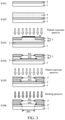
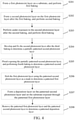
- the method may be implemented by the processing equipment. As shown in FIG. 2 and FIG. 3 , the method includes the following steps.
- S101 Form a first photoresist layer 2 on a substrate 1, and performing first baking.
- the first photoresist layer 2 is formed on the substrate 1 by spin coating, and the substrate 1 formed with the first photoresist layer 2 is baked at a soft bake temperature of the first photoresist layer 2, where the first photoresist layer 2 does not react with a developing solution for a second photoresist layer 3.
- the first photoresist layer 2 can protect the substrate 1 during the development of the second photoresist layer 3, thereby preventing the substrate 1 from being corroded by the developing solution.
- the provided substrate 1 should be clean, so as to provide good bonding between the substrate 1 and the film layer on the substrate.
- S102 Form a second photoresist layer 3 on the first photoresist layer 2 after the first baking, and perform second baking.
- the second photoresist layer 3 is formed on a side of the first photoresist layer 2 opposite to the substrate 1 by spin coating, and the second baking is performed at a soft bake temperature of the second photoresist layer 3.
- S103 Perform under exposure to the second photoresist layer 3 after the second baking, and perform third baking.
- a duration of the under exposure is less than a duration of full exposure of the second photoresist layer 3.
- the second photoresist layer 3 is partially exposed after the second photoresist layer 3 is baked, and the third baking is performed for a pre-baking time or a reversal baking time of the second photoresist layer 3.
- the under exposure may be implemented with an optical mask M.
- the second photoresist layer 3 is a negative photoresist
- the duration of exposure in this step is less than the duration of full exposure of the second photoresist layer 3, that is, the second photoresist layer 3 is underexposed
- the part of the second photoresist layer 3 distant from the substrate 1 reacts, and its properties being changed and becomes a reacted part 3a of the second photoresist layer 3
- the part of the second photoresist layer 3 approximate to the substrate 1 does not react, and it becomes an unreacted part 3b of the second photoresist layer 3. That is, through underexposure, the partially exposed second photoresist layer 3 has two parts: one that can be dissolved by the developing solution and the other that cannot be dissolved by the developing solution.
- the partially patterned second photoresist layer 3 includes a first opening.
- the first opening corresponds to an exposure area or a light-shielding area of the under exposure where was masked by the mask M.
- the first opening includes a first part 301 and a second part 302 located on a side of the first part 301 close to the substrate 1.
- An aperture of the first part 301 is smaller than an aperture of the second part 302.
- An orthographic projection of the first part 301 on the substrate 1 is within an orthographic projection of the second part 302 on the substrate 1.
- the first opening corresponds to the exposure area of the under exposure in S103. If the second photoresist layer 3 is a negative photoresist, the first opening corresponds to the light-shielding area of the under exposure in S103.
- the second photoresist layer 3 after the under exposure and the third baking is developed for a pre-set time, followed by fixing, where the pre-set time is at least 15s longer than a development time, in response to the second photoresist layer 3 being fully exposed.
- the pre-set time is at least 15s longer than a development time, in response to the second photoresist layer 3 being fully exposed.
- the size of the undercut can be controlled by adjusting the development time.
- S105 Flood exposing the partially patterned second photoresist layer 3, and performing fourth baking to determine a patterned second photoresist layer.
- the partially patterned second photoresist layer 3 (at this time, the unreacted part 3b of the second photoresist layer 3 has not been patterned) is flood exposed, and is baked sequentially at a pre-baking temperature and a hard baking temperature of the partially patterned second photoresist layer 3.
- the second photoresist layer 3 is flood exposed so that the unreacted part 3b of the second photoresist layer 3 reacts under light conditions, and the fourth baking is performed to harden the patterned second photoresist layer 3.
- the unreacted part 3b of the second photoresist layer 3 is likely to react with oxygen or other gases in the subsequent etching process to cause a change in size, while the reacted part 3a does not react with the gases in the etching process. Therefore, by the flood exposure of the partially patterned second photoresist layer 3, the unreacted portion 3b can be fully reacted to determine a fully reacted patterned second photoresist layer 3', thereby ensuring that the undercut structure has the preset size.
- S106 Etch the first photoresist layer 2 using the patterned second photoresist layer 3' as a mask to determine a patterned first photoresist layer 2'.
- the patterned first photoresist layer 2' includes a second opening 201, an aperture of the second opening 201 is smaller than the aperture of the second part 302 and greater than or equal to the aperture of the first part 301, and an orthographic projection of the second opening 201 on the substrate 1 is within an orthographic projection of the second part 302 on the substrate 1.
- the first photoresist layer 2 is etched by physical etching or reactive-ion etching using the patterned second photoresist layer 3' as a mask.
- the use of the determined patterned first photoresist layer 2' as a pattern restriction resist layer can effectively prevent lateral diffusion at the bottom of the deposited material during the material deposition process, thereby determining a patterned deposition layer having an actual size the same as the preset size.
- FIG. 8 and FIG. 9 A photoresist structure manufactured by the method for manufacturing a photoresist structure in the above embodiment is shown in FIG. 8 and FIG. 9 .
- the photoresist structure includes a patterned first photoresist layer 2 and a patterned second photoresist layer 3'.
- the patterned first photoresist layer 2' serves as a pattern restriction layer to prevent lateral diffusion at the bottom of the deposited material
- the patterned second photoresist layer 3' includes an undercut to prevent the deposited material from adhering to the sidewall of the photoresist structure.
- D1 is the size of the second opening 201 in the patterned first photoresist layer 2', that is, the size of the pattern restriction layer
- D2 is the size of the second part 302 of the first opening in the patterned second photoresist layer 3', that is, the size of the undercut
- D3 is a defined size of a patterned deposition layer 4'.
- the photoresist structure includes a patterned first photoresist layer 2' and a patterned second photoresist layer 3' located on the substrate 1.
- the patterned first photoresist layer 2' includes a plurality of second openings 201
- the patterned second photoresist layer 3' includes first openings corresponding one-to-one to the second openings 201.
- the first openings each include a first part 301 and a second part 302 located on a side of the first part 301 close to the substrate 1.
- An aperture of the first part 301 is smaller than an aperture of the second part 302.
- An orthographic projection of the first part 301 on the substrate 1 is within an orthographic projection of the second part 302 on the substrate 1.
- An aperture of the second opening 201 is smaller than the aperture of the second part 302 and greater than or equal to the aperture of the first part 301.
- An orthographic projection of the second opening 201 on the substrate 1 is within an orthographic projection of the second part 302 on the substrate 1.
- the photoresist structure not only can effectively prevent lateral diffusion at the bottom of the deposited material during the material deposition process, thereby determining a patterned deposition layer having an actual size the same as the preset size, but also can prevent the deposited material from adhering to the sidewall of the photoresist, thereby determining a patterned deposition layer with a good surface morphology.
- this specific embodiment includes the following steps:
- Step 1 Place a cleaned substrate, such as an aluminum substrate, on a spin-coating homogenizer, use a dropper to suck a polymethyl methacrylate (PMMA) resist, namely, acrylic resist, and drop it to the center of the aluminum substrate, run the homogenizer first at 300 rpm-800 rpm for 1s-5s and then at a 1000 rpm-6000 rpm for 30s-60s to determine a first photoresist layer 2; then place the aluminum substrate with the homogenized resist on a heating plate, and bake at a soft baking temperature of the PMMA resist (180°C) for 120s.
- PMMA polymethyl methacrylate
- Step 2 Place the aluminum substrate determined after step 1 on the spin-coating homogenizer, use a dropper to suck up a negative photoresist, drop it to the center of the aluminum substrate, and run the homogenizer first at 300 rpm-500 rpm for 1s-5s and then at 500 rpm-6000 rpm for 30s-60s to form a second photoresist layer 3; then place the aluminum substrate with the homogenized resist on the heating plate, and bake at a soft baking temperature of the negative photoresist, for example, at a certain temperature in the range of 90°C to 115°C, for a certain period of time, for example, 30s-120s.
- a soft baking temperature of the negative photoresist for example, at a certain temperature in the range of 90°C to 115°C, for a certain period of time, for example, 30s-120s.
- Step 3 Use an ultraviolet lithography machine to underexpose the aluminum substrate spin-coated with the two layers of resists, where the time of underexposure is less than the time for full exposure of the negative photoresist of the corresponding thickness that is determined in step 2. For example, for a 5 ⁇ m thick negative resist, the time for full exposure is 2.5s and the time for underexposure is 1.2s; then place the underexposed substrate on a hot plate and bake at a certain temperature for a certain period of time, for example, bake at 110°C for 90s.
- Step 4 Place the aluminum substrate determined after step 3 in a developing solution for the negative photoresist, for example, a 2.38% concentration of tetramethylammonium hydroxide (TMAH) solution for development, where the development time is at least 15s longer than the time for full development, for example, the development time is 80s-150s; then fix the substrate in deionized water for 30s-180s.
- TMAH tetramethylammonium hydroxide
- PMMA does not react with TMAH, which can protect the aluminum substrate from contact with the alkaline TMAH solution, thereby preventing the aluminum substrate from being corroded by the alkaline TMAH solution.
- each defined pattern includes a first photoresist layer 2 (PMMA resist) as a protective resist layer.
- Step 5 Use the ultraviolet lithography machine to flood expose the aluminum substrate determined after step 4, where the exposure time is, for example, 30s-180; then place the aluminum substrate on the hot plate and bake sequentially at the pre-baking and post-baking temperatures of the negative photoresist used as the second photoresist layer 3, for example, bake first at 110°C for 90s (seconds) and then at 110°C for 60s.
- Step 6 Place the aluminum substrate determined after step 5 in an etching equipment, such as a March resist remover, and etch for 3 min at a power of 300 W in an oxygen environment, to determine a photoresist structure shown in FIG. 8 .
- the photoresist structure includes a patterned first photoresist layer 2' and a patterned second photoresist layer 3'.
- the patterned first photoresist layer 2' is a pattern restriction layer
- the patterned second photoresist layer 3' includes an undercut.
- the first photoresist layer 2 (PMMA resist) in each defined pattern is completely etched within the range of the defined pattern.
- the above specific embodiments show a method for manufacturing a photoresist structure based on a negative photoresist and a PMMA resist.
- the thickness of the negative photoresist may be changed by changing the rotation speed during resist homogenization, and the size of the undercut may be changed by changing the exposure and development time.
- This method can meet different requirements of processing technologies, has high flexibility and is suitable for processes such as deposition, etching, and lift-off.
- the embodiments of this disclosure also provide a method for manufacturing a patterned deposition layer.
- the method for manufacturing a patterned deposition layer includes the method for manufacturing a photoresist structure in the above-mentioned embodiment, and therefore has the beneficial effects of the embodiment of the method for manufacturing a photoresist structure, which will not be repeated here.
- S201 to S206 in the method for manufacturing a patterned deposition layer of this embodiment respectively correspond to S101 to S106 in the embodiment of the method for manufacturing a photoresist structure.
- the method for manufacturing a patterned deposition layer of this embodiment further includes:
- S207 Form a deposition layer 4 on the patterned second photoresist layer 3' and on the substrate 1 exposed through the patterned first photoresist layer.
- a thickness of the deposition layer 4 is less than a sum of a thickness of the patterned first photoresist layer 2' and a thickness of the patterned second photoresist layer 3'.
- the thickness of the deposition layer 4 is made smaller than the sum of the thickness of the patterned first photoresist layer 2' and the thicknesses of the patterned second photoresist layer 3', so that the deposition layer 4 on the patterned second photoresist 3' is disconnected from the deposition layer 4 on the exposed substrate 1. In this way, the deposition layer 4 on the patterned second photoresist 3' can be removed at the same time by removing the photoresist.
- the substrate 1 formed with the deposition layer 4 is placed in a lift-off solution, and the first photoresist layer 2' and the patterned second photoresist layer 3' are removed at a temperature of 20 to 80°C, to determine the patterned deposition layer 4'.
- the patterned deposition layer 4' determined by the manufacturing method provided by this embodiment has a smooth surface, has a good surface morphology, and no lateral diffusion, and can be of the same size as the preset size.
- the first photoresist layer 2 and the second photoresist layer 3 can be photoresist that can react with the same kind of resist removal solution to achieve one-time peeling. Thereby reducing the peeling difficulty and peeling cost.
- the deposition layer may be a metal deposition layer.
- the deposition layer may be a source/drain electrode, an indium pillar, etc. in a chip.
- the deposition layer may also be a non-metal deposition layer.
- the deposition layer may be a non-metallic insulation structure located between two conductive layers to bridge the two conductive layers.
- the first photoresist layer 2 and the second photoresist layer 3 may be photoresists that can react with the same kind of resist removal solution to realize lift-off at a time, thereby reducing the difficulty of lift-off and the cost of lift-off.
- the embodiments of this disclosure also provide a method for manufacturing a semiconductor chip.
- the method for manufacturing a semiconductor chip includes the method for manufacturing a patterned deposition layer in the above-mentioned embodiment, and therefore has the beneficial effects of the embodiment of the method for manufacturing a patterned deposition layer, which will not be repeated here.
- the method for manufacturing a semiconductor chip provided in this embodiment further includes steps such as cutting and packaging, which will not be detailed here because the points of invention of this disclosure do not involve processes such as cutting and packaging of the semiconductor chip.
- the embodiments of this disclosure also provide a semiconductor chip.
- a patterned deposition layer included in the semiconductor chip provided in this embodiment is manufactured by the method for manufacturing a patterned deposition layer in the above-mentioned embodiment, and therefore has the beneficial effects of the embodiment of the method for manufacturing a patterned deposition layer, which will not be repeated here.
- a single photoresist is used, a second photoresist layer having an undercut can be determined by only one development process using a single developing solution, and the size of the undercut can be controlled by the development time, thereby solving the problems such as difficulty in lift-off caused by adhesion of the deposited material to the sidewall of the photoresist structure in traditional lift-off processes.
- the use of the first photoresist layer as a protective resist layer can protect the substrate material from being corroded or damaged by the developing solution during development.
- the first photoresist layer serving as a protective resist layer is etched to be a pattern restriction layer, which can effectively prevent the lateral diffusion of the bottom of the deposited material during the material deposition process, thereby determining a deposition layer with good morphology.
- the first photoresist layer and the second photoresist layer may be photoresists that can react with the same kind of resist removal solution to realize lift-off at a time, thereby reducing the difficulty of lift-off and the cost of lift-off.
- embodiments of this disclosure further provide a storage medium, the storage medium being configured to store a computer program, the computer program being configured to execute the method in the foregoing embodiments.
- the embodiments of this disclosure further provide a computer program product including instructions, the instructions, when run on a computer, causing the computer to execute the method according to the foregoing embodiments.
- first and second are used merely for the purpose of description, and shall not be construed as indicating or implying relative importance or implying a quantity of indicated technical features. Therefore, a feature limited by “first” or “second” may explicitly or implicitly include one or more of the features. In the description of this disclosure, unless otherwise stated, "a plurality of" means two or more than two.
- connection may be a fixed connection, a detachable connection, or an integral connection; or the connection may be a direct connection, an indirect connection through an intermediary, or internal communication between two components.
- steps in the flowchart in the accompanying drawings are sequentially shown according to indication of an arrow, the steps are not necessarily sequentially performed according to a sequence indicated by the arrow. Unless explicitly specified in this specification, execution of the steps is not strictly limited in the sequence, and the steps may be performed in other sequences.
- steps in the flowcharts in the accompanying drawings may include a plurality of substeps or a plurality of stages. The substeps or the stages are not necessarily performed at the same moment, but may be performed at different moments. The substeps or the stages are not necessarily performed in sequence, but may be performed in turn or alternately with another step or at least some of substeps or stages of the another step.
Landscapes
- Physics & Mathematics (AREA)
- General Physics & Mathematics (AREA)
- Engineering & Computer Science (AREA)
- Architecture (AREA)
- Structural Engineering (AREA)
- Photosensitive Polymer And Photoresist Processing (AREA)
- Exposure And Positioning Against Photoresist Photosensitive Materials (AREA)
Abstract
Description
- This disclosure claims priority to
Chinese Patent Application No. 202010717981.7, entitled "Photoresist structure, patterned deposition layer, semiconductor chip and manufacturing method thereof" filed on July 23, 2020 - The invention relates to the technical field of micro-nano processing, and in particular, to a photoresist structure, a patterned deposition layer and a semiconductor chip.
- In the field of micro-nano processing technology, most of the processing techniques such as the lift-off process need to be realized by preparing a special photoresist structure.
- Taking the lift-off process as an example, conventional technologies have the following problems. First, the sidewall of the deposited material is likely to adhere to the sidewall of the photoresist, resulting in poor morphology of the patterned deposition layer. Second, in the photoresist patterning process, the developing solution reacts with the substrate material, causing corrosion to the substrate material.
- The first problem can usually be solved by preparing a photoresist structure having an undercut, but the photoresist structure having an undercut is likely to cause lateral diffusion of the bottom of the deposited material, resulting in that the actual size of the patterned deposition layer does not match the defined size.
- In conventional technical solutions, the second problem can only be solved by selecting a photoresist that uses a developing solution that does not react with the substrate material, but this will reduce the compatibility of the process.
- In view of the shortcomings of the existing methods, this disclosure provides a photoresist structure, a patterned deposition layer, a semiconductor chip, and a manufacturing method thereof. When the method is used in a lift-off process, a good effect is achieved, and the size of the patterned deposition layer after lift-off is consistent with the defined pattern size.
- According to one aspect, the embodiments of this disclosure provide a method for manufacturing a photoresist structure, including the following steps:
- forming a first photoresist layer on a substrate, and performing first baking;
- forming a second photoresist layer on the first photoresist layer after the first baking, and performing second baking;
- performing under exposure to the second photoresist layer after the second baking, and performing third baking, a duration of the under exposure being less than a duration of full exposure of the second photoresist layer;
- developing and fixing the second photoresist layer after the third baking to determine a partially patterned second photoresist layer, the partially patterned second photoresist layer comprising a first opening, the first opening corresponding to an exposure area or a light-shielding area for the under exposure, the first opening comprising a first part and a second part located on a side of the first part close to the substrate, an aperture of the first part being smaller than an aperture of the second part, and an orthographic projection of the first part on the substrate is within an orthographic projection of the second part on the substrate;
- flood exposing the partially patterned second photoresist layer, and performing fourth baking to determine a patterned second photoresist layer; and
- etching the first photoresist layer using the patterned second photoresist layer as a mask to determine a patterned first photoresist layer.
- Optionally, the forming a first photoresist layer on a substrate, and performing first baking includes: forming the first photoresist layer on the substrate by spin coating, and baking the substrate formed with the first photoresist layer at a soft bake temperature of the first photoresist layer, where the first photoresist layer does not react with a developing solution for the second photoresist layer.
- Optionally, the forming a second photoresist layer on the first photoresist layer after the first baking, and performing second baking includes: forming the second photoresist layer on a side of the first photoresist layer opposite to the substrate by spin coating, and performing the second baking at a soft bake temperature of the second photoresist layer.
- Optionally, the performing under exposure to the second photoresist layer after the second baking, and performing third baking includes: partially exposing the second photoresist layer after the second baking, and performing the third baking for a pre-baking time or a reversal baking time of the second photoresist layer.
- Optionally, the developing and fixing the second photoresist layer after the third baking includes: developing the second photoresist layer after the under exposure and the third baking for a pre-set time, followed by fixing, where the pre-set time is at least 15 seconds longer than a development time for fully exposing the second photoresist layer.
- Optionally, the performing fourth baking to determine a patterned second photoresist layer includes: baking sequentially at a pre-baking temperature and a hardbake temperature of the partially patterned second photoresist layer, to determine the patterned second photoresist layer.
- Optionally, the etching the first photoresist layer using the patterned second photoresist layer as a mask includes: etching the first photoresist layer by physical etching and/or reactive-ion etching using the patterned second photoresist layer as the mask.
- According to another aspect, the embodiments of this disclosure provide a method for manufacturing a patterned deposition layer, the method including:
- determining a photoresist structure, the photoresist structure being manufactured by the above-mentioned method for manufacturing a photoresist structure;
- forming a deposition layer on the patterned second photoresist layer and on the substrate exposed through the patterned first photoresist layer, a thickness of the deposition layer being less than a sum of a thickness of chip, the patterned first photoresist layer and a thickness of the patterned second photoresist layer; and
- removing the patterned first photoresist layer and the patterned second photoresist layer to determine a patterned deposition layer.
- According to another aspect, the embodiments of this disclosure provide a method for manufacturing a semiconductor chip, a patterned deposition layer included in the semiconductor chip being manufactured by the above-mentioned method for manufacturing a patterned deposition layer.
- According to another aspect, the embodiments of this disclosure provide a semiconductor chip, a patterned deposition layer included in the semiconductor chip being manufactured by the above-mentioned method for manufacturing a patterned deposition layer.
- According to yet another aspect, the embodiments of this disclosure provide a computer device, including:
- a processor, a communication interface, a memory, and a communication bus,
- the processor, the communication interface, and the memory communicating with each other by using the communication bus; and the communication interface being an interface of a communication module;
- the memory being configured to store program code and transmit the program code to the processor; and the processor being configured to call instructions in the program code in the memory to execute the methods of the above aspects.
- According to yet another aspect, an embodiment of this disclosure provides a storage medium, the storage medium being configured to store a computer program, the computer program being configured to execute the method according to the above aspect.
- According to yet another aspect, an embodiment of this disclosure provides a computer program product including instructions, the computer program product, when run on a computer, causing the computer to execute the method according to the above aspect.
- Compared with the prior art, the present invention has the following advantages and beneficial effects:
According to the photoresist structure, patterned deposition layer, semiconductor chip and manufacturing method thereof provided in this disclosure, by means of underexposure, a single photoresist is used, a second photoresist layer having an undercut can be determined by only one development process using a single developing solution, and the size of the undercut can be controlled by the development time, thereby solving the problems such as difficulty in lift-off caused by adhesion of the deposited material to the sidewall of the photoresist structure in traditional lift-off processes. The use of the first photoresist layer as a protective resist layer can protect the substrate material from being corroded or damaged by the developing solution during development. The first photoresist layer serving as a protective resist layer is etched into a pattern restriction layer, which can effectively prevent the lateral diffusion of the bottom of the deposited material during the material deposition process, thereby determining a deposition layer with good morphology. In addition, the first photoresist layer and the second photoresist layer may be photoresists that can react with the same kind of resist removal solution to realize lift-off at a time, thereby reducing the difficulty of lift-off and the cost of lift-off. - Additional aspects and advantages of this disclosure will be given in part in the following description, and will become apparent from the following description or may be learned from practices of this disclosure.
- The foregoing and/or additional aspects and advantages of this disclosure will become obvious and easy to understand from the following descriptions of the embodiments with reference to the accompanying drawings.
-
FIG. 1 is a schematic cross-sectional view of a photoresist structure having an undercut in the related art. -
FIG. 2 is a schematic flowchart of a method for manufacturing a photoresist structure according to an embodiment of this disclosure. -
FIG. 3 is a schematic process diagram of the method for manufacturing a photoresist structure shown inFIG. 2 . -
FIG. 4 is a schematic flowchart of a method for manufacturing a patterned deposition layer according to an embodiment of this disclosure. -
FIG. 5 is a schematic process diagram of the processes of S207 and S208 in the method for manufacturing a patterned deposition layer shown inFIG. 4 . -
FIG. 6 is a schematic top view of a photoresist structure before etching according to an embodiment of this disclosure. -
FIG. 7 is a schematic top view of a photoresist structure after etching according to an embodiment of this disclosure. -
FIG. 8 is an electron scanning electron microscope image of a photoresist structure after etching according to an embodiment of this disclosure. -
FIG. 9 is a schematic top view of a photoresist structure after etching according to an embodiment of this disclosure. -
FIG. 10 is an electron scanning electron microscope image of a patterned deposition layer according to an embodiment of this disclosure. - 1 - substrate; 2 - first photoresist layer; 2' - patterned first photoresist layer; 201 - second opening; 3 - second photoresist layer; 3a - reacted part; 3b - unreacted part; 3' - patterned second photoresist layer; 301 - first part; 302 - second part; 4 - deposition layer; 4' - patterned deposition layer; M - exposure mask.
- This disclosure is described in detail below, and examples of the embodiments are shown in accompanying drawings, where the same or similar elements or the elements having same or similar functions are denoted by the same or similar reference numerals throughout the description. In addition, a detailed description of known technologies will be omitted if it is not necessary for the illustrated features of this disclosure. The embodiments that are described below with reference to the accompanying drawings are exemplary, and are only used to interpret this disclosure and cannot be construed as a limitation to this disclosure.
- It may be understood by those skilled in the art that unless otherwise defined, all terms (including technical and scientific terms) used herein have the same meaning as commonly understood by one of ordinary skill in the art to which this disclosure belongs. The terms such as those defined in commonly used dictionaries are to be interpreted as having meanings that are consistent with the meanings in the context of the related art, and are not to be interpreted in an idealized or extremely formalized sense, unless expressively so defined herein.
- A person skilled in the art may understand that, the singular forms "a", "an", "said", and "the" used herein may include the plural forms as well, unless the context clearly indicates otherwise. It is to be further understood that, the terms "include" and/or "comprise" used in this specification of this disclosure refer to the presence of stated features, integers, steps, operations, elements, and/or components, but do not preclude the presence or addition of one or more other features, integers, steps, operations, elements, components, and/or combinations thereof.
- First, several terms included in this disclosure are described and explained.
- Undercut: It is a photoresist structure and often refers to a structure having a bottom wider than its top, with its sidewall gradually expanding outward from the top to the bottom. The cross-section of the photoresist is in the shape of a regular trapezoid, and may also be in a shape of two stacked rectangles, where the bottom one is wider that the top one.
- Underexposure: It means that the exposure time for the photoresist is less than the time required for the photoresist with the thickness to completely react.
- Flood exposure: Full exposure of the photoresist on the substrate.
- Considering that the deposited material is likely to adhere to the sidewall of the photoresist in the process of determining the patterned deposition layer, the related technologies adopt a photoresist structure having an undercut to prevent the deposited material from adhering to the sidewall of the photoresist. However, the photoresist structure having an undercut is likely to cause lateral diffusion of the bottom of the deposited material, affecting the size of the patterned deposition layer, and reducing the performance of the chip prepared.
- Specifically, in a related technology, as shown in
FIG. 1 , asecond photoresist layer 3 and afirst photoresist layer 2 are sequentially formed on asubstrate 1. Thefirst photoresist layer 2 and thesecond photoresist layer 3 are formed with an undercut. Although the undercut can prevent thedeposition layer 4 from adhering to the photoresist, lateral diffusion of the bottom of thedeposition layer 4 is caused. As a result, the size of the bottom of the finally determineddeposition layer 4 of a specific shape is larger, and is different from the pre-designed size of thedeposition layer 4 of the specific shape. - The photoresist structure, patterned deposition layer, semiconductor chip and manufacturing method thereof provided by the embodiments of this disclosure aim to solve the technical problems of the related technologies.
- The embodiments provided in this disclosure can be implemented by various processing equipment involved in the field of micro-nano processing technology. The processing equipment can implement various functions required for manufacture of a photoresist structure, manufacture of a patterned deposition layer, and manufacture of a semiconductor chip in the field of micro-nano processing technology.
- The processing equipment may include a homogenizer, a lithography machine (for example, an ultraviolet lithography machine, etc.), and an etching equipment (for example, a March resist remover, etc.).
- The following describes the technical solutions of this disclosure and how to resolve the foregoing technical issues according to the technical solutions of this disclosure in detail by using specific embodiments.
- An embodiment of this disclosure provides a method for manufacturing a photoresist structure. The method may be implemented by the processing equipment. As shown in
FIG. 2 andFIG. 3 , the method includes the following steps. - S101: Form a
first photoresist layer 2 on asubstrate 1, and performing first baking. - Specifically, in this step, the
first photoresist layer 2 is formed on thesubstrate 1 by spin coating, and thesubstrate 1 formed with thefirst photoresist layer 2 is baked at a soft bake temperature of thefirst photoresist layer 2, where thefirst photoresist layer 2 does not react with a developing solution for asecond photoresist layer 3. In this way, thefirst photoresist layer 2 can protect thesubstrate 1 during the development of thesecond photoresist layer 3, thereby preventing thesubstrate 1 from being corroded by the developing solution. Further, the providedsubstrate 1 should be clean, so as to provide good bonding between thesubstrate 1 and the film layer on the substrate. - S102: Form a
second photoresist layer 3 on thefirst photoresist layer 2 after the first baking, and perform second baking. - Specifically, in this step, the
second photoresist layer 3 is formed on a side of thefirst photoresist layer 2 opposite to thesubstrate 1 by spin coating, and the second baking is performed at a soft bake temperature of thesecond photoresist layer 3. - S103: Perform under exposure to the
second photoresist layer 3 after the second baking, and perform third baking. - A duration of the under exposure is less than a duration of full exposure of the
second photoresist layer 3. - Specifically, in this step, the
second photoresist layer 3 is partially exposed after thesecond photoresist layer 3 is baked, and the third baking is performed for a pre-baking time or a reversal baking time of thesecond photoresist layer 3. As shown inFIG. 3 , the under exposure may be implemented with an optical mask M. In an example where thesecond photoresist layer 3 is a negative photoresist, because the duration of exposure in this step is less than the duration of full exposure of thesecond photoresist layer 3, that is, thesecond photoresist layer 3 is underexposed, the part of thesecond photoresist layer 3 distant from thesubstrate 1 reacts, and its properties being changed and becomes a reacted part 3a of thesecond photoresist layer 3; the part of thesecond photoresist layer 3 approximate to thesubstrate 1 does not react, and it becomes anunreacted part 3b of thesecond photoresist layer 3. That is, through underexposure, the partially exposedsecond photoresist layer 3 has two parts: one that can be dissolved by the developing solution and the other that cannot be dissolved by the developing solution. - S104: Develop and fix the
second photoresist layer 3 after the third baking to determine a partially patternedsecond photoresist layer 3. - The partially patterned
second photoresist layer 3 includes a first opening. The first opening corresponds to an exposure area or a light-shielding area of the under exposure where was masked by the mask M. The first opening includes afirst part 301 and asecond part 302 located on a side of thefirst part 301 close to thesubstrate 1. An aperture of thefirst part 301 is smaller than an aperture of thesecond part 302. An orthographic projection of thefirst part 301 on thesubstrate 1 is within an orthographic projection of thesecond part 302 on thesubstrate 1. - Specifically, if the
second photoresist layer 3 is a positive photoresist, the first opening corresponds to the exposure area of the under exposure in S103. If thesecond photoresist layer 3 is a negative photoresist, the first opening corresponds to the light-shielding area of the under exposure in S103. - Specifically, in this step, the
second photoresist layer 3 after the under exposure and the third baking is developed for a pre-set time, followed by fixing, where the pre-set time is at least 15s longer than a development time, in response to thesecond photoresist layer 3 being fully exposed. With the longer development time, an undercut can be formed in thesecond photoresist layer 3, thereby preventing the deposited material from adhering to the sidewall of the photoresist. The size of the undercut can be controlled by adjusting the development time. - S105: Flood exposing the partially patterned
second photoresist layer 3, and performing fourth baking to determine a patterned second photoresist layer. - Specifically, in this step, the partially patterned second photoresist layer 3 (at this time, the
unreacted part 3b of thesecond photoresist layer 3 has not been patterned) is flood exposed, and is baked sequentially at a pre-baking temperature and a hard baking temperature of the partially patternedsecond photoresist layer 3. Thesecond photoresist layer 3 is flood exposed so that theunreacted part 3b of thesecond photoresist layer 3 reacts under light conditions, and the fourth baking is performed to harden the patternedsecond photoresist layer 3. - Since the
unreacted part 3b of thesecond photoresist layer 3 is likely to react with oxygen or other gases in the subsequent etching process to cause a change in size, while the reacted part 3a does not react with the gases in the etching process. Therefore, by the flood exposure of the partially patternedsecond photoresist layer 3, theunreacted portion 3b can be fully reacted to determine a fully reacted patterned second photoresist layer 3', thereby ensuring that the undercut structure has the preset size. - S106: Etch the
first photoresist layer 2 using the patterned second photoresist layer 3' as a mask to determine a patterned first photoresist layer 2'. - Specifically, the patterned first photoresist layer 2' includes a
second opening 201, an aperture of thesecond opening 201 is smaller than the aperture of thesecond part 302 and greater than or equal to the aperture of thefirst part 301, and an orthographic projection of thesecond opening 201 on thesubstrate 1 is within an orthographic projection of thesecond part 302 on thesubstrate 1. - Specifically, in this step, the
first photoresist layer 2 is etched by physical etching or reactive-ion etching using the patterned second photoresist layer 3' as a mask. The use of the determined patterned first photoresist layer 2' as a pattern restriction resist layer can effectively prevent lateral diffusion at the bottom of the deposited material during the material deposition process, thereby determining a patterned deposition layer having an actual size the same as the preset size. - A photoresist structure manufactured by the method for manufacturing a photoresist structure in the above embodiment is shown in
FIG. 8 and FIG. 9 . The photoresist structure includes a patternedfirst photoresist layer 2 and a patterned second photoresist layer 3'. The patterned first photoresist layer 2' serves as a pattern restriction layer to prevent lateral diffusion at the bottom of the deposited material, and the patterned second photoresist layer 3' includes an undercut to prevent the deposited material from adhering to the sidewall of the photoresist structure. - Specifically, as shown in
FIG. 9 and referring toFIG. 3 andFIG. 5 , D1 is the size of thesecond opening 201 in the patterned first photoresist layer 2', that is, the size of the pattern restriction layer; D2 is the size of thesecond part 302 of the first opening in the patterned second photoresist layer 3', that is, the size of the undercut; D3 is a defined size of a patterned deposition layer 4'. - Specifically, as shown in
FIG. 8 and FIG. 9 and referring toFIG. 3 , the photoresist structure includes a patterned first photoresist layer 2' and a patterned second photoresist layer 3' located on thesubstrate 1. The patterned first photoresist layer 2' includes a plurality ofsecond openings 201, and the patterned second photoresist layer 3' includes first openings corresponding one-to-one to thesecond openings 201. The first openings each include afirst part 301 and asecond part 302 located on a side of thefirst part 301 close to thesubstrate 1. An aperture of thefirst part 301 is smaller than an aperture of thesecond part 302. An orthographic projection of thefirst part 301 on thesubstrate 1 is within an orthographic projection of thesecond part 302 on thesubstrate 1. An aperture of thesecond opening 201 is smaller than the aperture of thesecond part 302 and greater than or equal to the aperture of thefirst part 301. An orthographic projection of thesecond opening 201 on thesubstrate 1 is within an orthographic projection of thesecond part 302 on thesubstrate 1. The photoresist structure not only can effectively prevent lateral diffusion at the bottom of the deposited material during the material deposition process, thereby determining a patterned deposition layer having an actual size the same as the preset size, but also can prevent the deposited material from adhering to the sidewall of the photoresist, thereby determining a patterned deposition layer with a good surface morphology. - For ease of understanding, the following embodiment provides a specific method for manufacturing a photoresist structure. A photoresist structure finally determine is shown in
FIG. 7 . Referring toFIG. 3 , this specific embodiment includes the following steps: - Step 1: Place a cleaned substrate, such as an aluminum substrate, on a spin-coating homogenizer, use a dropper to suck a polymethyl methacrylate (PMMA) resist, namely, acrylic resist, and drop it to the center of the aluminum substrate, run the homogenizer first at 300 rpm-800 rpm for 1s-5s and then at a 1000 rpm-6000 rpm for 30s-60s to determine a
first photoresist layer 2; then place the aluminum substrate with the homogenized resist on a heating plate, and bake at a soft baking temperature of the PMMA resist (180°C) for 120s. - Step 2: Place the aluminum substrate determined after
step 1 on the spin-coating homogenizer, use a dropper to suck up a negative photoresist, drop it to the center of the aluminum substrate, and run the homogenizer first at 300 rpm-500 rpm for 1s-5s and then at 500 rpm-6000 rpm for 30s-60s to form asecond photoresist layer 3; then place the aluminum substrate with the homogenized resist on the heating plate, and bake at a soft baking temperature of the negative photoresist, for example, at a certain temperature in the range of 90°C to 115°C, for a certain period of time, for example, 30s-120s. - Step 3: Use an ultraviolet lithography machine to underexpose the aluminum substrate spin-coated with the two layers of resists, where the time of underexposure is less than the time for full exposure of the negative photoresist of the corresponding thickness that is determined in
step 2. For example, for a 5 µm thick negative resist, the time for full exposure is 2.5s and the time for underexposure is 1.2s; then place the underexposed substrate on a hot plate and bake at a certain temperature for a certain period of time, for example, bake at 110°C for 90s. - Step 4: Place the aluminum substrate determined after
step 3 in a developing solution for the negative photoresist, for example, a 2.38% concentration of tetramethylammonium hydroxide (TMAH) solution for development, where the development time is at least 15s longer than the time for full development, for example, the development time is 80s-150s; then fix the substrate in deionized water for 30s-180s. In this process, PMMA does not react with TMAH, which can protect the aluminum substrate from contact with the alkaline TMAH solution, thereby preventing the aluminum substrate from being corroded by the alkaline TMAH solution. As shown inFIG. 6 , before the etching step (step 5), each defined pattern includes a first photoresist layer 2 (PMMA resist) as a protective resist layer. - Step 5: Use the ultraviolet lithography machine to flood expose the aluminum substrate determined after
step 4, where the exposure time is, for example, 30s-180; then place the aluminum substrate on the hot plate and bake sequentially at the pre-baking and post-baking temperatures of the negative photoresist used as thesecond photoresist layer 3, for example, bake first at 110°C for 90s (seconds) and then at 110°C for 60s. - Step 6: Place the aluminum substrate determined after step 5 in an etching equipment, such as a March resist remover, and etch for 3 min at a power of 300 W in an oxygen environment, to determine a photoresist structure shown in
FIG. 8 . The photoresist structure includes a patterned first photoresist layer 2' and a patterned second photoresist layer 3'. In the photoresist structure, the patterned first photoresist layer 2' is a pattern restriction layer, and the patterned second photoresist layer 3' includes an undercut. As shown inFIG. 7 , the first photoresist layer 2 (PMMA resist) in each defined pattern is completely etched within the range of the defined pattern. - The above specific embodiments show a method for manufacturing a photoresist structure based on a negative photoresist and a PMMA resist. In a specific implementation, the thickness of the negative photoresist may be changed by changing the rotation speed during resist homogenization, and the size of the undercut may be changed by changing the exposure and development time. This method can meet different requirements of processing technologies, has high flexibility and is suitable for processes such as deposition, etching, and lift-off.
- Based on the same inventive concept, the embodiments of this disclosure also provide a method for manufacturing a patterned deposition layer. The method for manufacturing a patterned deposition layer includes the method for manufacturing a photoresist structure in the above-mentioned embodiment, and therefore has the beneficial effects of the embodiment of the method for manufacturing a photoresist structure, which will not be repeated here.
- Specifically, as shown in
FIG. 4 , S201 to S206 in the method for manufacturing a patterned deposition layer of this embodiment respectively correspond to S101 to S106 in the embodiment of the method for manufacturing a photoresist structure. - Specifically, as shown in
FIG. 4 andFIG. 5 , the method for manufacturing a patterned deposition layer of this embodiment further includes: - S207: Form a
deposition layer 4 on the patterned second photoresist layer 3' and on thesubstrate 1 exposed through the patterned first photoresist layer. - A thickness of the
deposition layer 4 is less than a sum of a thickness of the patterned first photoresist layer 2' and a thickness of the patterned second photoresist layer 3'. - Specifically, by controlling the thickness of the patterned first photoresist layer 2' and the patterned second photoresist layer 3', the thickness of the
deposition layer 4 is made smaller than the sum of the thickness of the patterned first photoresist layer 2' and the thicknesses of the patterned second photoresist layer 3', so that thedeposition layer 4 on the patterned second photoresist 3' is disconnected from thedeposition layer 4 on the exposedsubstrate 1. In this way, thedeposition layer 4 on the patterned second photoresist 3' can be removed at the same time by removing the photoresist. - S208: Remove the patterned first photoresist layer 2' and the patterned second photoresist layer 3' to determine a patterned deposition layer 4'.
- Specifically, the
substrate 1 formed with thedeposition layer 4 is placed in a lift-off solution, and the first photoresist layer 2' and the patterned second photoresist layer 3' are removed at a temperature of 20 to 80°C, to determine the patterned deposition layer 4'. - As shown in
FIG. 10 , the patterned deposition layer 4' determined by the manufacturing method provided by this embodiment has a smooth surface, has a good surface morphology, and no lateral diffusion, and can be of the same size as the preset size. - In the method for fabricating a patterned deposition layer provided in this embodiment, the
first photoresist layer 2 and thesecond photoresist layer 3 can be photoresist that can react with the same kind of resist removal solution to achieve one-time peeling. Thereby reducing the peeling difficulty and peeling cost. - Specifically, the deposition layer may be a metal deposition layer. For example, the deposition layer may be a source/drain electrode, an indium pillar, etc. in a chip. The deposition layer may also be a non-metal deposition layer. For example, the deposition layer may be a non-metallic insulation structure located between two conductive layers to bridge the two conductive layers.
- In the method for fabricating a patterned deposition layer provided in this embodiment, the
first photoresist layer 2 and thesecond photoresist layer 3 may be photoresists that can react with the same kind of resist removal solution to realize lift-off at a time, thereby reducing the difficulty of lift-off and the cost of lift-off. - Based on the same inventive concept, the embodiments of this disclosure also provide a method for manufacturing a semiconductor chip. The method for manufacturing a semiconductor chip includes the method for manufacturing a patterned deposition layer in the above-mentioned embodiment, and therefore has the beneficial effects of the embodiment of the method for manufacturing a patterned deposition layer, which will not be repeated here.
- Specifically, the method for manufacturing a semiconductor chip provided in this embodiment further includes steps such as cutting and packaging, which will not be detailed here because the points of invention of this disclosure do not involve processes such as cutting and packaging of the semiconductor chip.
- Based on the same inventive concept, the embodiments of this disclosure also provide a semiconductor chip. A patterned deposition layer included in the semiconductor chip provided in this embodiment is manufactured by the method for manufacturing a patterned deposition layer in the above-mentioned embodiment, and therefore has the beneficial effects of the embodiment of the method for manufacturing a patterned deposition layer, which will not be repeated here.
- By applying the embodiments of this disclosure, at least the following beneficial effects can be achieved:
- According to the photoresist structure, patterned deposition layer, semiconductor chip and manufacturing method thereof provided in this disclosure, a single photoresist is used, a second photoresist layer having an undercut can be determined by only one development process using a single developing solution, and the size of the undercut can be controlled by the development time, thereby solving the problems such as difficulty in lift-off caused by adhesion of the deposited material to the sidewall of the photoresist structure in traditional lift-off processes. The use of the first photoresist layer as a protective resist layer can protect the substrate material from being corroded or damaged by the developing solution during development. The first photoresist layer serving as a protective resist layer is etched to be a pattern restriction layer, which can effectively prevent the lateral diffusion of the bottom of the deposited material during the material deposition process, thereby determining a deposition layer with good morphology. In addition, the first photoresist layer and the second photoresist layer may be photoresists that can react with the same kind of resist removal solution to realize lift-off at a time, thereby reducing the difficulty of lift-off and the cost of lift-off.
- In addition, the embodiments of this disclosure further provide a storage medium, the storage medium being configured to store a computer program, the computer program being configured to execute the method in the foregoing embodiments.
- The embodiments of this disclosure further provide a computer program product including instructions, the instructions, when run on a computer, causing the computer to execute the method according to the foregoing embodiments.
- It may be understood by a person skilled in the art that the steps, measures, and solutions in various operations, methods, and processes that have been discussed in this disclosure can be interchanged, modified, combined, or deleted. Further, other steps, measures, and solutions in various operations, methods, and processes that have been discussed in this disclosure can be interchanged, modified, rearranged, decomposed, combined, or deleted. Further, the steps, measures, and solutions in various operations, methods, and processes disclosed in this disclosure in the related art can be interchanged, modified, rearranged, decomposed, combined, or deleted.
- In the description of this disclosure, it is to be understood that a direction or location relationship indicated by a term "center", "on", "under", "front", "rear", "left", "right", "vertical", "horizontal", "top", "bottom", "inner", "outer", or the like is a direction or location relationship shown based on the accompanying drawings, and is intended only conveniently describe this disclosure and simplify the description, but is not intended to indicate or imply that a mentioned apparatus or element needs to have a particular direction and is constructed and operated in the particular direction. Therefore, the direction or location relationship cannot be understood as a limitation on this disclosure.
- The terms "first" and "second" are used merely for the purpose of description, and shall not be construed as indicating or implying relative importance or implying a quantity of indicated technical features. Therefore, a feature limited by "first" or "second" may explicitly or implicitly include one or more of the features. In the description of this disclosure, unless otherwise stated, "a plurality of" means two or more than two.
- In the description of this disclosure, it should be noted that unless otherwise explicitly specified or defined, the terms such as "mount", "connect", and "connection" should be understood in a broad sense. For example, the connection may be a fixed connection, a detachable connection, or an integral connection; or the connection may be a direct connection, an indirect connection through an intermediary, or internal communication between two components. A person of ordinary skill in the art may understand the specific meanings of the foregoing terms in this disclosure according to specific situations.
- In the descriptions of this specification, the described specific features, structures, materials, or characteristics may be combined in a proper manner in any one or more of the embodiments or examples.
- It is to be understood that, although the steps in the flowchart in the accompanying drawings are sequentially shown according to indication of an arrow, the steps are not necessarily sequentially performed according to a sequence indicated by the arrow. Unless explicitly specified in this specification, execution of the steps is not strictly limited in the sequence, and the steps may be performed in other sequences. In addition, at least some steps in the flowcharts in the accompanying drawings may include a plurality of substeps or a plurality of stages. The substeps or the stages are not necessarily performed at the same moment, but may be performed at different moments. The substeps or the stages are not necessarily performed in sequence, but may be performed in turn or alternately with another step or at least some of substeps or stages of the another step.
- The foregoing descriptions are some implementations of this disclosure. A person of ordinary skill in the art may make several improvements and refinements without departing from the principle of this disclosure, and the improvements and refinements shall fall within the protection scope of this disclosure.
Claims (13)
- A method for manufacturing a photoresist structure, performed by a processing device, and comprising:forming a first photoresist layer on a substrate, and performing first baking;forming a second photoresist layer on the first photoresist layer after the first baking, and performing second baking;performing under exposure to the second photoresist layer after the second baking, and performing third baking, a duration of the under exposure being less than a duration of full exposure of the second photoresist layer;developing and fixing the second photoresist layer after the third baking to determine a partially patterned second photoresist layer, the partially patterned second photoresist layer comprising a first opening, the first opening corresponding to an exposure area or a light-shielding area for the under exposure, the first opening comprising a first part and a second part located on a side of the first part close to the substrate, an aperture of the first part being smaller than an aperture of the second part, and an orthographic projection of the first part on the substrate is within an orthographic projection of the second part on the substrate;flood exposing the partially patterned second photoresist layer, and performing fourth baking to determine a patterned second photoresist layer; andetching the first photoresist layer using the patterned second photoresist layer as a mask to determine a patterned first photoresist layer.
- The method for manufacturing a photoresist structure according to claim 1, wherein the forming a first photoresist layer on a substrate, and performing first baking comprises:
forming the first photoresist layer on the substrate by spin coating, and baking the substrate formed with the first photoresist layer at a soft bake temperature of the first photoresist layer, wherein the first photoresist layer does not react with a developing solution for the second photoresist layer. - The method for manufacturing a photoresist structure according to claim 1, wherein the forming a second photoresist layer on the first photoresist layer after the first baking, and performing second baking comprises:
forming the second photoresist layer on a side of the first photoresist layer opposite to the substrate by spin coating, and performing the second baking at a soft bake temperature of the second photoresist layer. - The method for manufacturing a photoresist structure according to claim 1, wherein the performing under exposure to the second photoresist layer after the second baking, and performing third baking comprises:
partially exposing the second photoresist layer after the second baking, and performing the third baking for a pre-baking time or a reversal baking time of the second photoresist layer. - The method for manufacturing a photoresist structure according to claim 1, wherein the developing and fixing the second photoresist layer after the third baking comprises:
developing the second photoresist layer after the under exposure and the third baking for a preset time, followed by fixing, wherein the pre-set time is at least 15 seconds longer than a development time for fully exposing the second photoresist layer. - The method for manufacturing a photoresist structure according to any one of claims 1-5, wherein the performing fourth baking to determine a patterned second photoresist layer comprises:
baking sequentially at a pre-baking temperature and a hardbake temperature of the partially patterned second photoresist layer, to determine the patterned second photoresist layer. - The method for manufacturing a photoresist structure according to any one of claims 1-5, wherein the etching the first photoresist layer using the patterned second photoresist layer as a mask comprises:
etching the first photoresist layer by physical etching and/or reactive-ion etching using the patterned second photoresist layer as the mask. - A method for manufacturing a patterned deposition layer, the method comprising:determining a photoresist structure, the photoresist structure being manufactured by the method for manufacturing a photoresist structure according to any one of claims 1-7;forming a deposition layer on the patterned second photoresist layer and on the substrate exposed through the patterned first photoresist layer, a thickness of the deposition layer being less than a sum of a thickness of the patterned first photoresist layer and a thickness of the patterned second photoresist layer; andremoving the patterned first photoresist layer and the patterned second photoresist layer to determine a patterned deposition layer.
- A method for manufacturing a semiconductor chip, a patterned deposition layer comprised in the semiconductor chip being manufactured by the method for manufacturing a patterned deposition layer according to claim 8.
- A semiconductor chip, a patterned deposition layer comprised in the semiconductor chip being manufactured by the method for manufacturing a patterned deposition layer according to claim 8.
- A computer device, comprising:a processor, a communication interface, a memory, and a communication bus,the processor, the communication interface, and the memory communicating with each other by using the communication bus; and the communication interface being an interface of a communication module;the memory being configured to store program code and transmit the program code to the processor; andthe processor being configured to call instructions in the program code in the memory to execute the method for manufacturing a photoresist structure according to any one of claims 1-7, or to execute the method for manufacturing a patterned deposition layer according to claim 8.
- A storage medium, configured to store a computer program, the computer program being configured to execute the method for manufacturing a photoresist structure according to any one of claims 1-7, or to execute the method for manufacturing a patterned deposition layer according to claim 8.
- A computer program product comprising instructions, the computer program product, when run on a computer, causing the computer to execute the method for manufacturing a photoresist structure according to any one of claims 1-7, or execute the method for manufacturing a patterned deposition layer according to claim 8.
Applications Claiming Priority (2)
| Application Number | Priority Date | Filing Date | Title |
|---|---|---|---|
| CN202010717981.7A CN112652522B (en) | 2020-07-23 | 2020-07-23 | Photoresist structure, patterned deposition layer, semiconductor chip and manufacturing method thereof |
| PCT/CN2021/100057 WO2022017073A1 (en) | 2020-07-23 | 2021-06-15 | Photoresist structure, patterned deposition layer, semiconductor chip and manufacturing method therefor |
Publications (3)
| Publication Number | Publication Date |
|---|---|
| EP3971946A1 true EP3971946A1 (en) | 2022-03-23 |
| EP3971946A4 EP3971946A4 (en) | 2022-08-03 |
| EP3971946B1 EP3971946B1 (en) | 2024-08-28 |
Family
ID=75346268
Family Applications (1)
| Application Number | Title | Priority Date | Filing Date |
|---|---|---|---|
| EP21783120.5A Active EP3971946B1 (en) | 2020-07-23 | 2021-06-15 | Photoresist structure, patterned deposition layer, semiconductor chip and manufacturing method therefor |
Country Status (6)
| Country | Link |
|---|---|
| US (1) | US12040188B2 (en) |
| EP (1) | EP3971946B1 (en) |
| JP (1) | JP7282440B2 (en) |
| KR (1) | KR102699407B1 (en) |
| CN (1) | CN112652522B (en) |
| WO (1) | WO2022017073A1 (en) |
Cited By (1)
| Publication number | Priority date | Publication date | Assignee | Title |
|---|---|---|---|---|
| EP3961680A4 (en) * | 2020-07-01 | 2022-07-20 | Tencent Technology (Shenzhen) Company Limited | METHOD OF MAKING INDIUM COLUMN SOLDER JOINT, CHIP SUBSTRATE AND CHIP |
Families Citing this family (10)
| Publication number | Priority date | Publication date | Assignee | Title |
|---|---|---|---|---|
| CN112652522B (en) | 2020-07-23 | 2022-05-03 | 腾讯科技(深圳)有限公司 | Photoresist structure, patterned deposition layer, semiconductor chip and manufacturing method thereof |
| CN112271133A (en) * | 2020-09-25 | 2021-01-26 | 华东光电集成器件研究所 | Metal stripping method based on three layers of glue |
| JP7304967B2 (en) * | 2020-11-17 | 2023-07-07 | テンセント・テクノロジー・(シェンジェン)・カンパニー・リミテッド | Air bridge manufacturing method, air bridge and electronic device |
| CN113193094B (en) * | 2021-04-27 | 2023-03-21 | 成都辰显光电有限公司 | Batch transfer method and display panel |
| CN114122090B (en) * | 2021-11-15 | 2023-08-01 | 深圳市华星光电半导体显示技术有限公司 | Processing method of photoresist layer, manufacturing method of display panel and display panel |
| CN116230505A (en) * | 2023-03-09 | 2023-06-06 | 浙江珏芯微电子有限公司 | Method for forming semiconductor pattern and method for manufacturing cooled infrared detector |
| CN116736636A (en) * | 2023-06-19 | 2023-09-12 | 无锡奥夫特光学技术有限公司 | A new photoresist structure and production method that improves high-temperature deformation of photoresist |
| CN119170490A (en) * | 2023-06-19 | 2024-12-20 | 本源量子计算科技(合肥)股份有限公司 | Mask and method for manufacturing the same, and method for manufacturing a Josephson junction |
| CN118545677A (en) * | 2024-05-28 | 2024-08-27 | 山东产研微纳与智能制造研究院有限公司 | Preparation method of thick metal patterning |
| CN121237637A (en) * | 2025-12-01 | 2025-12-30 | 合肥晶合集成电路股份有限公司 | Patterning methods and photoresist structures |
Family Cites Families (28)
| Publication number | Priority date | Publication date | Assignee | Title |
|---|---|---|---|---|
| US4533624A (en) * | 1983-05-23 | 1985-08-06 | Sperry Corporation | Method of forming a low temperature multilayer photoresist lift-off pattern |
| JPS61156044A (en) * | 1984-12-27 | 1986-07-15 | Nec Corp | Production of resist stencil mask |
| JPH08293454A (en) * | 1995-04-25 | 1996-11-05 | Nec Corp | Formation method for resist pattern |
| JP2765561B2 (en) * | 1996-03-29 | 1998-06-18 | 日本電気株式会社 | Fabrication method of fine aerial wiring |
| US7229745B2 (en) * | 2004-06-14 | 2007-06-12 | Bae Systems Information And Electronic Systems Integration Inc. | Lithographic semiconductor manufacturing using a multi-layered process |
| CN1688017A (en) | 2005-04-27 | 2005-10-26 | 福州大学 | PECVD deposition SiN film stripping technique |
| GB2442030A (en) | 2006-09-19 | 2008-03-26 | Innos Ltd | Resist exposure and patterning process |
| JP4899986B2 (en) | 2007-03-28 | 2012-03-21 | Jsr株式会社 | Two-layer laminated film and pattern forming method using the same |
| US7960097B2 (en) | 2007-10-30 | 2011-06-14 | Triquint Semiconductor, Inc. | Methods of minimizing etch undercut and providing clean metal liftoff |
| CN100594434C (en) * | 2007-12-27 | 2010-03-17 | 中国科学院物理研究所 | Method for fabricating metallic structures with large areas covered by metallic films on the nanometer scale |
| KR101301080B1 (en) | 2008-03-17 | 2013-09-03 | 삼성전자주식회사 | Method of Fabricating Triode-structure Field-emission device |
| CN101881927A (en) * | 2010-07-16 | 2010-11-10 | 中国科学院长春光学精密机械与物理研究所 | A method for preparing inverted trapezoidal photoresist cross section |
| CN102136484B (en) * | 2010-11-26 | 2013-01-09 | 中国科学院上海技术物理研究所 | Indium columns for face-down bonding interconnection of infrared focal plane and preparation method thereof |
| CN103094096A (en) * | 2011-11-07 | 2013-05-08 | 上海华虹Nec电子有限公司 | Peeling craft method used for forming semiconductor component metal graph |
| CN103107067B (en) * | 2011-11-14 | 2015-10-14 | 上海华虹宏力半导体制造有限公司 | A kind of process for making of semiconducting bi-layer protective layer |
| CN103137441A (en) * | 2011-11-22 | 2013-06-05 | 上海华虹Nec电子有限公司 | Method for manufacturing elongated isolated line pattern in semiconductor process |
| CN103137442B (en) * | 2011-11-30 | 2015-06-03 | 上海华虹宏力半导体制造有限公司 | Method of manufacturing slender type isolated line patterns in semiconductor technology |
| CN103035492B (en) * | 2012-05-28 | 2015-06-03 | 上海华虹宏力半导体制造有限公司 | Manufacturing method for double protection layers in semiconductor device |
| CN103107252B (en) * | 2013-02-27 | 2016-01-27 | 中国科学院物理研究所 | The method of class spherical structure is prepared on the GaP surface of AlGaInP base LED |
| CN105334699B (en) * | 2014-06-24 | 2018-11-20 | 中芯国际集成电路制造(上海)有限公司 | The method for improving photoresist pattern by repeated exposure |
| CN105116685B (en) | 2015-09-24 | 2019-10-01 | 京东方科技集团股份有限公司 | A kind of production method of photoetching agent pattern, colored filter and display device |
| CN105575892B (en) * | 2015-12-17 | 2018-04-03 | 武汉高芯科技有限公司 | A kind of process of infrared detector indium post |
| EP3685451B1 (en) | 2017-09-18 | 2021-01-13 | Google LLC | Reducing junction resistance variation in two-step deposition processes |
| CN108735582A (en) | 2018-04-09 | 2018-11-02 | 中国电子科技集团公司第十研究所 | A kind of preparation method of photoresist film |
| CN111221226A (en) * | 2018-11-27 | 2020-06-02 | 上海微电子装备(集团)股份有限公司 | Post-exposure baking method and device for photoresist layer |
| CN111399338B (en) * | 2020-04-30 | 2023-03-28 | 合肥本源量子计算科技有限责任公司 | Photoetching method |
| CN112652540B (en) * | 2020-07-01 | 2022-04-22 | 腾讯科技(深圳)有限公司 | Indium column welding spot preparation method, chip substrate and chip |
| CN112652522B (en) * | 2020-07-23 | 2022-05-03 | 腾讯科技(深圳)有限公司 | Photoresist structure, patterned deposition layer, semiconductor chip and manufacturing method thereof |
-
2020
- 2020-07-23 CN CN202010717981.7A patent/CN112652522B/en active Active
-
2021
- 2021-06-15 WO PCT/CN2021/100057 patent/WO2022017073A1/en not_active Ceased
- 2021-06-15 JP JP2021564350A patent/JP7282440B2/en active Active
- 2021-06-15 EP EP21783120.5A patent/EP3971946B1/en active Active
- 2021-06-15 KR KR1020217035960A patent/KR102699407B1/en active Active
- 2021-10-15 US US17/502,705 patent/US12040188B2/en active Active
Cited By (1)
| Publication number | Priority date | Publication date | Assignee | Title |
|---|---|---|---|---|
| EP3961680A4 (en) * | 2020-07-01 | 2022-07-20 | Tencent Technology (Shenzhen) Company Limited | METHOD OF MAKING INDIUM COLUMN SOLDER JOINT, CHIP SUBSTRATE AND CHIP |
Also Published As
| Publication number | Publication date |
|---|---|
| EP3971946A4 (en) | 2022-08-03 |
| CN112652522A (en) | 2021-04-13 |
| US20220037148A1 (en) | 2022-02-03 |
| KR102699407B1 (en) | 2024-08-28 |
| EP3971946B1 (en) | 2024-08-28 |
| CN112652522B (en) | 2022-05-03 |
| JP2022545050A (en) | 2022-10-25 |
| JP7282440B2 (en) | 2023-05-29 |
| WO2022017073A1 (en) | 2022-01-27 |
| KR20220013358A (en) | 2022-02-04 |
| US12040188B2 (en) | 2024-07-16 |
Similar Documents
| Publication | Publication Date | Title |
|---|---|---|
| US12040188B2 (en) | Photoresist structure, patterned deposition layer, semiconductor chip and manufacturing method thereof | |
| JP7206422B2 (en) | Method for preparing indium bump solder joints, chip substrates and chips | |
| CN112103241B (en) | Air bridge manufacturing method, air bridge and electronic equipment | |
| WO2017049878A1 (en) | Photoresist pattern forming method, color filter, and display device | |
| CN104656306A (en) | Substrate provided with black matrix, manufacturing method of substrate and display device | |
| CN106653774B (en) | Array substrate, manufacturing method thereof, mask plate, and display device | |
| CN108269736B (en) | Method for patterning electrode layer by photoresist stripping | |
| JP7124959B2 (en) | Semiconductor device manufacturing method | |
| US20180239179A1 (en) | Method for manufacturing spacers and method for manufacturing display substrate | |
| JP2002151381A (en) | Pattern formation method | |
| US20210408070A1 (en) | Array substrate and method for fabricating same | |
| HK40042597A (en) | Photoresist structure, patterned deposition layer, semiconductor chip and its manufacturing method | |
| HK40042597B (en) | Photoresist structure, patterned deposition layer, semiconductor chip and its manufacturing method | |
| CN108010923B (en) | TFT substrate manufacturing method | |
| CN113130383B (en) | Semiconductor structure and manufacturing method thereof | |
| EP4030468B1 (en) | Method for manufacturing air bridge | |
| CN106298643A (en) | The manufacture method of a kind of via and the manufacture method of display base plate | |
| KR0147468B1 (en) | Method for forming pattern during manufacturing semiconductor device | |
| HK40042596B (en) | Preparation method, chip substrate and chip for indium column solder joints | |
| JPH1138224A (en) | Color filter | |
| WO2021134688A1 (en) | Method for producing mems drive | |
| CN108376643A (en) | Manufacturing method, array substrate and the display device of array substrate | |
| TW200409193A (en) | Method for forming photoresist pattern | |
| WO2019153149A1 (en) | Flexible substrate and preparation method therefor, and electronic device | |
| JP2004177455A (en) | Manufacturing method of optical device molding die and optical device molding die |
Legal Events
| Date | Code | Title | Description |
|---|---|---|---|
| STAA | Information on the status of an ep patent application or granted ep patent |
Free format text: STATUS: UNKNOWN |
|
| STAA | Information on the status of an ep patent application or granted ep patent |
Free format text: STATUS: THE INTERNATIONAL PUBLICATION HAS BEEN MADE |
|
| PUAI | Public reference made under article 153(3) epc to a published international application that has entered the european phase |
Free format text: ORIGINAL CODE: 0009012 |
|
| STAA | Information on the status of an ep patent application or granted ep patent |
Free format text: STATUS: REQUEST FOR EXAMINATION WAS MADE |
|
| 17P | Request for examination filed |
Effective date: 20211014 |
|
| AK | Designated contracting states |
Kind code of ref document: A1 Designated state(s): AL AT BE BG CH CY CZ DE DK EE ES FI FR GB GR HR HU IE IS IT LI LT LU LV MC MK MT NL NO PL PT RO RS SE SI SK SM TR |
|
| RAP3 | Party data changed (applicant data changed or rights of an application transferred) |
Owner name: TENCENT TECHNOLOGY (SHENZHEN) COMPANY LIMITED |
|
| A4 | Supplementary search report drawn up and despatched |
Effective date: 20220706 |
|
| RIC1 | Information provided on ipc code assigned before grant |
Ipc: H01L 21/027 20060101AFI20220630BHEP |
|
| DAV | Request for validation of the european patent (deleted) | ||
| DAX | Request for extension of the european patent (deleted) | ||
| GRAP | Despatch of communication of intention to grant a patent |
Free format text: ORIGINAL CODE: EPIDOSNIGR1 |
|
| STAA | Information on the status of an ep patent application or granted ep patent |
Free format text: STATUS: GRANT OF PATENT IS INTENDED |
|
| RIC1 | Information provided on ipc code assigned before grant |
Ipc: H01L 21/311 20060101ALI20240510BHEP Ipc: G03F 7/40 20060101ALI20240510BHEP Ipc: G03F 7/38 20060101ALI20240510BHEP Ipc: G03F 7/20 20060101ALI20240510BHEP Ipc: G03F 7/16 20060101ALI20240510BHEP Ipc: G03F 7/095 20060101ALI20240510BHEP Ipc: H01L 21/027 20060101AFI20240510BHEP |
|
| INTG | Intention to grant announced |
Effective date: 20240619 |
|
| GRAS | Grant fee paid |
Free format text: ORIGINAL CODE: EPIDOSNIGR3 |
|
| GRAA | (expected) grant |
Free format text: ORIGINAL CODE: 0009210 |
|
| STAA | Information on the status of an ep patent application or granted ep patent |
Free format text: STATUS: THE PATENT HAS BEEN GRANTED |
|
| AK | Designated contracting states |
Kind code of ref document: B1 Designated state(s): AL AT BE BG CH CY CZ DE DK EE ES FI FR GB GR HR HU IE IS IT LI LT LU LV MC MK MT NL NO PL PT RO RS SE SI SK SM TR |
|
| REG | Reference to a national code |
Ref country code: CH Ref legal event code: EP |
|
| REG | Reference to a national code |
Ref country code: DE Ref legal event code: R096 Ref document number: 602021018024 Country of ref document: DE |
|
| REG | Reference to a national code |
Ref country code: IE Ref legal event code: FG4D |
|
| REG | Reference to a national code |
Ref country code: LT Ref legal event code: MG9D |
|
| PG25 | Lapsed in a contracting state [announced via postgrant information from national office to epo] |
Ref country code: NO Free format text: LAPSE BECAUSE OF FAILURE TO SUBMIT A TRANSLATION OF THE DESCRIPTION OR TO PAY THE FEE WITHIN THE PRESCRIBED TIME-LIMIT Effective date: 20241128 |
|
| REG | Reference to a national code |
Ref country code: AT Ref legal event code: MK05 Ref document number: 1718954 Country of ref document: AT Kind code of ref document: T Effective date: 20240828 |
|
| PG25 | Lapsed in a contracting state [announced via postgrant information from national office to epo] |
Ref country code: NL Free format text: LAPSE BECAUSE OF FAILURE TO SUBMIT A TRANSLATION OF THE DESCRIPTION OR TO PAY THE FEE WITHIN THE PRESCRIBED TIME-LIMIT Effective date: 20240828 Ref country code: PL Free format text: LAPSE BECAUSE OF FAILURE TO SUBMIT A TRANSLATION OF THE DESCRIPTION OR TO PAY THE FEE WITHIN THE PRESCRIBED TIME-LIMIT Effective date: 20240828 Ref country code: GR Free format text: LAPSE BECAUSE OF FAILURE TO SUBMIT A TRANSLATION OF THE DESCRIPTION OR TO PAY THE FEE WITHIN THE PRESCRIBED TIME-LIMIT Effective date: 20241129 Ref country code: PT Free format text: LAPSE BECAUSE OF FAILURE TO SUBMIT A TRANSLATION OF THE DESCRIPTION OR TO PAY THE FEE WITHIN THE PRESCRIBED TIME-LIMIT Effective date: 20241230 Ref country code: FI Free format text: LAPSE BECAUSE OF FAILURE TO SUBMIT A TRANSLATION OF THE DESCRIPTION OR TO PAY THE FEE WITHIN THE PRESCRIBED TIME-LIMIT Effective date: 20240828 |
|
| PG25 | Lapsed in a contracting state [announced via postgrant information from national office to epo] |
Ref country code: BG Free format text: LAPSE BECAUSE OF FAILURE TO SUBMIT A TRANSLATION OF THE DESCRIPTION OR TO PAY THE FEE WITHIN THE PRESCRIBED TIME-LIMIT Effective date: 20240828 |
|
| PG25 | Lapsed in a contracting state [announced via postgrant information from national office to epo] |
Ref country code: LV Free format text: LAPSE BECAUSE OF FAILURE TO SUBMIT A TRANSLATION OF THE DESCRIPTION OR TO PAY THE FEE WITHIN THE PRESCRIBED TIME-LIMIT Effective date: 20240828 |
|
| REG | Reference to a national code |
Ref country code: NL Ref legal event code: MP Effective date: 20240828 |
|
| PG25 | Lapsed in a contracting state [announced via postgrant information from national office to epo] |
Ref country code: IS Free format text: LAPSE BECAUSE OF FAILURE TO SUBMIT A TRANSLATION OF THE DESCRIPTION OR TO PAY THE FEE WITHIN THE PRESCRIBED TIME-LIMIT Effective date: 20241228 Ref country code: AT Free format text: LAPSE BECAUSE OF FAILURE TO SUBMIT A TRANSLATION OF THE DESCRIPTION OR TO PAY THE FEE WITHIN THE PRESCRIBED TIME-LIMIT Effective date: 20240828 |
|
| PG25 | Lapsed in a contracting state [announced via postgrant information from national office to epo] |
Ref country code: HR Free format text: LAPSE BECAUSE OF FAILURE TO SUBMIT A TRANSLATION OF THE DESCRIPTION OR TO PAY THE FEE WITHIN THE PRESCRIBED TIME-LIMIT Effective date: 20240828 |
|
| PG25 | Lapsed in a contracting state [announced via postgrant information from national office to epo] |
Ref country code: ES Free format text: LAPSE BECAUSE OF FAILURE TO SUBMIT A TRANSLATION OF THE DESCRIPTION OR TO PAY THE FEE WITHIN THE PRESCRIBED TIME-LIMIT Effective date: 20240828 Ref country code: RS Free format text: LAPSE BECAUSE OF FAILURE TO SUBMIT A TRANSLATION OF THE DESCRIPTION OR TO PAY THE FEE WITHIN THE PRESCRIBED TIME-LIMIT Effective date: 20241128 |
|
| PG25 | Lapsed in a contracting state [announced via postgrant information from national office to epo] |
Ref country code: RS Free format text: LAPSE BECAUSE OF FAILURE TO SUBMIT A TRANSLATION OF THE DESCRIPTION OR TO PAY THE FEE WITHIN THE PRESCRIBED TIME-LIMIT Effective date: 20241128 Ref country code: PT Free format text: LAPSE BECAUSE OF FAILURE TO SUBMIT A TRANSLATION OF THE DESCRIPTION OR TO PAY THE FEE WITHIN THE PRESCRIBED TIME-LIMIT Effective date: 20241230 Ref country code: PL Free format text: LAPSE BECAUSE OF FAILURE TO SUBMIT A TRANSLATION OF THE DESCRIPTION OR TO PAY THE FEE WITHIN THE PRESCRIBED TIME-LIMIT Effective date: 20240828 Ref country code: NO Free format text: LAPSE BECAUSE OF FAILURE TO SUBMIT A TRANSLATION OF THE DESCRIPTION OR TO PAY THE FEE WITHIN THE PRESCRIBED TIME-LIMIT Effective date: 20241128 Ref country code: NL Free format text: LAPSE BECAUSE OF FAILURE TO SUBMIT A TRANSLATION OF THE DESCRIPTION OR TO PAY THE FEE WITHIN THE PRESCRIBED TIME-LIMIT Effective date: 20240828 Ref country code: LV Free format text: LAPSE BECAUSE OF FAILURE TO SUBMIT A TRANSLATION OF THE DESCRIPTION OR TO PAY THE FEE WITHIN THE PRESCRIBED TIME-LIMIT Effective date: 20240828 Ref country code: IS Free format text: LAPSE BECAUSE OF FAILURE TO SUBMIT A TRANSLATION OF THE DESCRIPTION OR TO PAY THE FEE WITHIN THE PRESCRIBED TIME-LIMIT Effective date: 20241228 Ref country code: HR Free format text: LAPSE BECAUSE OF FAILURE TO SUBMIT A TRANSLATION OF THE DESCRIPTION OR TO PAY THE FEE WITHIN THE PRESCRIBED TIME-LIMIT Effective date: 20240828 Ref country code: GR Free format text: LAPSE BECAUSE OF FAILURE TO SUBMIT A TRANSLATION OF THE DESCRIPTION OR TO PAY THE FEE WITHIN THE PRESCRIBED TIME-LIMIT Effective date: 20241129 Ref country code: FI Free format text: LAPSE BECAUSE OF FAILURE TO SUBMIT A TRANSLATION OF THE DESCRIPTION OR TO PAY THE FEE WITHIN THE PRESCRIBED TIME-LIMIT Effective date: 20240828 Ref country code: ES Free format text: LAPSE BECAUSE OF FAILURE TO SUBMIT A TRANSLATION OF THE DESCRIPTION OR TO PAY THE FEE WITHIN THE PRESCRIBED TIME-LIMIT Effective date: 20240828 Ref country code: BG Free format text: LAPSE BECAUSE OF FAILURE TO SUBMIT A TRANSLATION OF THE DESCRIPTION OR TO PAY THE FEE WITHIN THE PRESCRIBED TIME-LIMIT Effective date: 20240828 Ref country code: AT Free format text: LAPSE BECAUSE OF FAILURE TO SUBMIT A TRANSLATION OF THE DESCRIPTION OR TO PAY THE FEE WITHIN THE PRESCRIBED TIME-LIMIT Effective date: 20240828 |
|
| PG25 | Lapsed in a contracting state [announced via postgrant information from national office to epo] |
Ref country code: SM Free format text: LAPSE BECAUSE OF FAILURE TO SUBMIT A TRANSLATION OF THE DESCRIPTION OR TO PAY THE FEE WITHIN THE PRESCRIBED TIME-LIMIT Effective date: 20240828 Ref country code: RO Free format text: LAPSE BECAUSE OF FAILURE TO SUBMIT A TRANSLATION OF THE DESCRIPTION OR TO PAY THE FEE WITHIN THE PRESCRIBED TIME-LIMIT Effective date: 20240828 Ref country code: DK Free format text: LAPSE BECAUSE OF FAILURE TO SUBMIT A TRANSLATION OF THE DESCRIPTION OR TO PAY THE FEE WITHIN THE PRESCRIBED TIME-LIMIT Effective date: 20240828 |
|
| PG25 | Lapsed in a contracting state [announced via postgrant information from national office to epo] |
Ref country code: EE Free format text: LAPSE BECAUSE OF FAILURE TO SUBMIT A TRANSLATION OF THE DESCRIPTION OR TO PAY THE FEE WITHIN THE PRESCRIBED TIME-LIMIT Effective date: 20240828 |
|
| PG25 | Lapsed in a contracting state [announced via postgrant information from national office to epo] |
Ref country code: CZ Free format text: LAPSE BECAUSE OF FAILURE TO SUBMIT A TRANSLATION OF THE DESCRIPTION OR TO PAY THE FEE WITHIN THE PRESCRIBED TIME-LIMIT Effective date: 20240828 |
|
| PG25 | Lapsed in a contracting state [announced via postgrant information from national office to epo] |
Ref country code: IT Free format text: LAPSE BECAUSE OF FAILURE TO SUBMIT A TRANSLATION OF THE DESCRIPTION OR TO PAY THE FEE WITHIN THE PRESCRIBED TIME-LIMIT Effective date: 20240828 Ref country code: SK Free format text: LAPSE BECAUSE OF FAILURE TO SUBMIT A TRANSLATION OF THE DESCRIPTION OR TO PAY THE FEE WITHIN THE PRESCRIBED TIME-LIMIT Effective date: 20240828 |
|
| REG | Reference to a national code |
Ref country code: DE Ref legal event code: R097 Ref document number: 602021018024 Country of ref document: DE |
|
| PLBE | No opposition filed within time limit |
Free format text: ORIGINAL CODE: 0009261 |
|
| STAA | Information on the status of an ep patent application or granted ep patent |
Free format text: STATUS: NO OPPOSITION FILED WITHIN TIME LIMIT |
|
| PGFP | Annual fee paid to national office [announced via postgrant information from national office to epo] |
Ref country code: DE Payment date: 20250618 Year of fee payment: 5 |
|
| PGFP | Annual fee paid to national office [announced via postgrant information from national office to epo] |
Ref country code: GB Payment date: 20250620 Year of fee payment: 5 |
|
| PGFP | Annual fee paid to national office [announced via postgrant information from national office to epo] |
Ref country code: FR Payment date: 20250613 Year of fee payment: 5 |
|
| 26N | No opposition filed |
Effective date: 20250530 |
|
| PG25 | Lapsed in a contracting state [announced via postgrant information from national office to epo] |
Ref country code: SE Free format text: LAPSE BECAUSE OF FAILURE TO SUBMIT A TRANSLATION OF THE DESCRIPTION OR TO PAY THE FEE WITHIN THE PRESCRIBED TIME-LIMIT Effective date: 20240828 |
|
| REG | Reference to a national code |
Ref country code: DE Ref legal event code: R079 Ref document number: 602021018024 Country of ref document: DE Free format text: PREVIOUS MAIN CLASS: H01L0021027000 Ipc: H10P0076000000 |
|
| REG | Reference to a national code |
Ref country code: CH Ref legal event code: H13 Free format text: ST27 STATUS EVENT CODE: U-0-0-H10-H13 (AS PROVIDED BY THE NATIONAL OFFICE) Effective date: 20260127 |
|
| PG25 | Lapsed in a contracting state [announced via postgrant information from national office to epo] |
Ref country code: MC Free format text: LAPSE BECAUSE OF FAILURE TO SUBMIT A TRANSLATION OF THE DESCRIPTION OR TO PAY THE FEE WITHIN THE PRESCRIBED TIME-LIMIT Effective date: 20240828 |
|
| PG25 | Lapsed in a contracting state [announced via postgrant information from national office to epo] |
Ref country code: LU Free format text: LAPSE BECAUSE OF NON-PAYMENT OF DUE FEES Effective date: 20250615 |
|
| REG | Reference to a national code |
Ref country code: BE Ref legal event code: MM Effective date: 20250630 |
|
| PG25 | Lapsed in a contracting state [announced via postgrant information from national office to epo] |
Ref country code: IE Free format text: LAPSE BECAUSE OF NON-PAYMENT OF DUE FEES Effective date: 20250615 |
|
| PG25 | Lapsed in a contracting state [announced via postgrant information from national office to epo] |
Ref country code: BE Free format text: LAPSE BECAUSE OF NON-PAYMENT OF DUE FEES Effective date: 20250630 |
|
| PG25 | Lapsed in a contracting state [announced via postgrant information from national office to epo] |
Ref country code: CH Free format text: LAPSE BECAUSE OF NON-PAYMENT OF DUE FEES Effective date: 20250630 |