EP3968346B1 - Wireless power transfer thin profile coil assembly - Google Patents
Wireless power transfer thin profile coil assembly Download PDFInfo
- Publication number
- EP3968346B1 EP3968346B1 EP21203177.7A EP21203177A EP3968346B1 EP 3968346 B1 EP3968346 B1 EP 3968346B1 EP 21203177 A EP21203177 A EP 21203177A EP 3968346 B1 EP3968346 B1 EP 3968346B1
- Authority
- EP
- European Patent Office
- Prior art keywords
- conductor
- conductor pattern
- coil
- wireless power
- power transfer
- Prior art date
- Legal status (The legal status is an assumption and is not a legal conclusion. Google has not performed a legal analysis and makes no representation as to the accuracy of the status listed.)
- Active
Links
Images


Classifications
-
- H—ELECTRICITY
- H01—ELECTRIC ELEMENTS
- H01F—MAGNETS; INDUCTANCES; TRANSFORMERS; SELECTION OF MATERIALS FOR THEIR MAGNETIC PROPERTIES
- H01F27/00—Details of transformers or inductances, in general
- H01F27/28—Coils; Windings; Conductive connections
- H01F27/2804—Printed windings
-
- H—ELECTRICITY
- H01—ELECTRIC ELEMENTS
- H01F—MAGNETS; INDUCTANCES; TRANSFORMERS; SELECTION OF MATERIALS FOR THEIR MAGNETIC PROPERTIES
- H01F27/00—Details of transformers or inductances, in general
- H01F27/28—Coils; Windings; Conductive connections
- H01F27/2847—Sheets; Strips
-
- H—ELECTRICITY
- H01—ELECTRIC ELEMENTS
- H01F—MAGNETS; INDUCTANCES; TRANSFORMERS; SELECTION OF MATERIALS FOR THEIR MAGNETIC PROPERTIES
- H01F27/00—Details of transformers or inductances, in general
- H01F27/28—Coils; Windings; Conductive connections
- H01F27/2871—Pancake coils
-
- H—ELECTRICITY
- H01—ELECTRIC ELEMENTS
- H01F—MAGNETS; INDUCTANCES; TRANSFORMERS; SELECTION OF MATERIALS FOR THEIR MAGNETIC PROPERTIES
- H01F27/00—Details of transformers or inductances, in general
- H01F27/34—Special means for preventing or reducing unwanted electric or magnetic effects, e.g. no-load losses, reactive currents, harmonics, oscillations, leakage fields
- H01F27/36—Electric or magnetic shields or screens
- H01F27/361—Electric or magnetic shields or screens made of combinations of electrically conductive material and ferromagnetic material
-
- H—ELECTRICITY
- H01—ELECTRIC ELEMENTS
- H01F—MAGNETS; INDUCTANCES; TRANSFORMERS; SELECTION OF MATERIALS FOR THEIR MAGNETIC PROPERTIES
- H01F27/00—Details of transformers or inductances, in general
- H01F27/34—Special means for preventing or reducing unwanted electric or magnetic effects, e.g. no-load losses, reactive currents, harmonics, oscillations, leakage fields
- H01F27/36—Electric or magnetic shields or screens
- H01F27/363—Electric or magnetic shields or screens made of electrically conductive material
-
- H—ELECTRICITY
- H01—ELECTRIC ELEMENTS
- H01F—MAGNETS; INDUCTANCES; TRANSFORMERS; SELECTION OF MATERIALS FOR THEIR MAGNETIC PROPERTIES
- H01F27/00—Details of transformers or inductances, in general
- H01F27/34—Special means for preventing or reducing unwanted electric or magnetic effects, e.g. no-load losses, reactive currents, harmonics, oscillations, leakage fields
- H01F27/36—Electric or magnetic shields or screens
- H01F27/366—Electric or magnetic shields or screens made of ferromagnetic material
-
- H—ELECTRICITY
- H01—ELECTRIC ELEMENTS
- H01F—MAGNETS; INDUCTANCES; TRANSFORMERS; SELECTION OF MATERIALS FOR THEIR MAGNETIC PROPERTIES
- H01F27/00—Details of transformers or inductances, in general
- H01F27/40—Structural association with built-in electric component, e.g. fuse
- H01F27/402—Association of measuring or protective means
-
- H—ELECTRICITY
- H01—ELECTRIC ELEMENTS
- H01F—MAGNETS; INDUCTANCES; TRANSFORMERS; SELECTION OF MATERIALS FOR THEIR MAGNETIC PROPERTIES
- H01F38/00—Adaptations of transformers or inductances for specific applications or functions
- H01F38/14—Inductive couplings
-
- H—ELECTRICITY
- H01—ELECTRIC ELEMENTS
- H01F—MAGNETS; INDUCTANCES; TRANSFORMERS; SELECTION OF MATERIALS FOR THEIR MAGNETIC PROPERTIES
- H01F5/00—Coils
- H01F5/003—Printed circuit coils
-
- H—ELECTRICITY
- H02—GENERATION; CONVERSION OR DISTRIBUTION OF ELECTRIC POWER
- H02J—CIRCUIT ARRANGEMENTS OR SYSTEMS FOR SUPPLYING OR DISTRIBUTING ELECTRIC POWER; SYSTEMS FOR STORING ELECTRIC ENERGY
- H02J50/00—Circuit arrangements or systems for wireless supply or distribution of electric power
- H02J50/10—Circuit arrangements or systems for wireless supply or distribution of electric power using inductive coupling
- H02J50/12—Circuit arrangements or systems for wireless supply or distribution of electric power using inductive coupling of the resonant type
-
- H—ELECTRICITY
- H04—ELECTRIC COMMUNICATION TECHNIQUE
- H04B—TRANSMISSION
- H04B5/00—Near-field transmission systems, e.g. inductive or capacitive transmission systems
- H04B5/70—Near-field transmission systems, e.g. inductive or capacitive transmission systems specially adapted for specific purposes
- H04B5/79—Near-field transmission systems, e.g. inductive or capacitive transmission systems specially adapted for specific purposes for data transfer in combination with power transfer
-
- H—ELECTRICITY
- H01—ELECTRIC ELEMENTS
- H01F—MAGNETS; INDUCTANCES; TRANSFORMERS; SELECTION OF MATERIALS FOR THEIR MAGNETIC PROPERTIES
- H01F27/00—Details of transformers or inductances, in general
- H01F27/28—Coils; Windings; Conductive connections
- H01F27/2804—Printed windings
- H01F2027/2809—Printed windings on stacked layers
-
- H—ELECTRICITY
- H01—ELECTRIC ELEMENTS
- H01F—MAGNETS; INDUCTANCES; TRANSFORMERS; SELECTION OF MATERIALS FOR THEIR MAGNETIC PROPERTIES
- H01F27/00—Details of transformers or inductances, in general
- H01F27/34—Special means for preventing or reducing unwanted electric or magnetic effects, e.g. no-load losses, reactive currents, harmonics, oscillations, leakage fields
- H01F2027/348—Preventing eddy currents
Definitions
- Resonant induction wireless charging makes use of an air core transformer consisting of two concentric coils displaced along a common coil axis. Electrical power is sent from the sending apparatus to the receiving apparatus by means of magnetic flux linkage between the two transfer coils. A high frequency alternating current flowing in the primary coil induces an alternating current into the secondary coil.
- Litz wire has a number of disadvantages in this application. Litz wire has poor utilization of cross-sectional area due to void space between the individual wires and also due to the significant portion of the cross-section occupied by individual wire insulation. The insulation and void space volumes make heat removal from the Litz bundle interior difficult. Finally, Litz wire is costly and assembly operations involving Litz wire especially wire forming and connector attachment are labor intensive.
- a method of designing and constructing resonant induction transfer coils that avoids the disadvantageous use of Litz wire is desired.
- US 2013/222101 A1 concerns a coil component that includes: an insulating resin layer provided between a first planar spiral conductor formed on a back surface of a first substrate and a second planar spiral conductor formed on a back surface of a second substrate; an upper core covering a third planar spiral conductor formed on a front surface of the first substrate on which the insulating resin layer is formed; and a lower core covering a fourth planar spiral conductor formed on a front surface of the second substrate on which the insulating resin layer is formed.
- EP 3016231 A1 describes a power transmission device having a surface a part of which defines a power transmission plane. The device is suitable for the wireless charging of mobile devices within vehicles.
- the device includes: a power transmission coil structure including 2N planar coils laminated in a perpendicular direction to the power transmission plane and wirelessly transmitting AC power to a power receiving device via the power transmission plane and being disposed on a side toward the power transmission plane; and a magnetic substance disposed on a side of the power transmission coil opposite from the power transmission plane, wherein the 2N planar coils constitute coil groups including a coil group in which an i'th closest planar coil to the power transmission plane out of the 2N planar coils and the i'th-closest planar coil to the magnetic substance out of the 2N planar coils are connected in series, and the coil groups are connected in parallel to each other.
- US 2015/077208 A1 describes a parallel-trace spiral coil comprising a plurality of electrically-isolated, parallel connected metal traces with high Q factor for use in bio-medical implants.
- the invention is a resonant induction wireless power transfer coil as defined in the appended claims.
- a resonant induction, wireless power transfer coil includes a printed circuit board backed by a layer of flux guiding ferrite magnetic material inside a weatherproof enclosure. Additional components include resonating capacitors, rectifiers and post-rectification ripple filters that are included in the weatherproof enclosure.
- the multiple, independent individual printed circuit board traces correspond to the multiple independent Litz wire conductors present in conventional transfer coils. Trace width is selected to minimize conductor eddy currents and proximity effects. The overall trace pattern insures current sharing among multiple traces.
- the resulting planar spiral inductor described herein has low AC resistance and can be easily and inexpensively manufactured as a conventional printed circuit board.
- Sample embodiments include a resonant induction wireless power transfer coil including a 2n-layer coil stack, where n is a positive integer.
- the 2n-layer coil stack includes a dielectric connected to operate in a differential mode and having a first side and a second side, a first conductor pattern including a first plurality of conductors wound in a spiral on the first side of the dielectric to provide a forward current path conductor, and a second conductor pattern comprising a second plurality of conductors wound in a spiral on the second side of the dielectric to provide a return current path conductor.
- the second conductor pattern is aligned with the first conductor pattern whereby the second conductor pattern reinforces magnetic flux generated by the first conductor pattern.
- the 2n-layer coil stack is characterised in that the first and second conductor patterns are not directly electrically connected.
- the dielectric may comprise a printed circuit board having a first side and a second side, the first conductor pattern comprising a first plurality of conductors wound in a spiral on the first side of the printed circuit board, and the second conductor pattern comprising a second plurality of conductors wound in a spiral on the second side of the printed circuit board.
- At least one electrical connection may be provided to electrically connect respective conductors of the first and second conductor patterns.
- the electrical connections may comprise at least one throughhole through the printed circuit board or at least one or more of a clamp, a lug, and a terminal.
- the throughholes may also be plated offset throughholes.
- the first and second conductor patterns may comprise at least 2 turns of conductor configured as a square, flat planar spiral and the first and second plurality of conductors may each comprise at least two independent conductors.
- the trace thickness is limited by the skin depth at the operating frequency as it contributes to AC resistance.
- the trace width is limited by the allowable conductor eddy currents.
- Trace-to-trace spacing is minimized to manufacturing capability as voltage between traces are close to zero. Turn-to-turn proximity effects minimize trace-to-trace proximity effects. Turn-to-turn spacing is minimized to the limits allowed by turn-to-turn voltage.
- the wireless power transfer coil may further include coil terminals and associated throughholes in the center of the first and second conductor patterns or at an outer edge of the first and second conductor patterns and an outer edge of the printed circuit board.
- the wireless power transfer coil also may comprise a multi-layer coil stack comprising 2n layers having the first and second conductor patterns, where n is a positive integer.
- the multi-layer coil stack comprises a first conductor pattern providing a forward current path conductor, a second conductor pattern providing a return current path conductor, and a dielectric connected to operate in a differential mode that is provided between the first conductor pattern and the second conductor pattern.
- the multi-layer coil stack respectively comprises a first conductor pattern providing a forward current path conductor, a second conductor pattern providing a return current path conductor, a third conductor pattern providing a forward current path conductor, a fourth conductor pattern providing a return current path conductor, a first dielectric provided between the first conductor pattern and the second conductor pattern connected to operate in a differential mode, a second differential mode dielectric provided between the third conductor pattern and the fourth conductor pattern connected to operate in a differential mode, and a third differential mode dielectric provided between the second conductor pattern and the third conductor pattern connected to operate in a differential mode.
- the multi-layer coil stack respectively comprises a first conductor pattern providing a forward current path conductor, a second conductor pattern providing a return current path conductor, a third conductor pattern providing a return current path conductor, a fourth conductor pattern providing a forward current path conductor, a first dielectric provided between the first conductor pattern and the second conductor pattern connected to operate in a differential mode, a second dielectric provided between the third conductor pattern and the fourth conductor pattern connected to operate in a differential mode, and a third dielectric provided between the second conductor pattern and the third conductor pattern connected to operate in a common mode.
- the multi-layer coil stack respectively comprises a first conductor pattern providing a first forward current path conductor, a second conductor pattern providing a second forward current path conductor, a third conductor pattern providing a first return current path conductor, a fourth conductor pattern providing a second return current path conductor, a first dielectric provided between the first conductor pattern and the second conductor pattern connected to operate in a common mode, a second dielectric provided between the third conductor pattern and the fourth conductor pattern connected to operate in a common mode, and a third dielectric provided between the second conductor pattern and the third conductor pattern connected to operate in a differential mode.
- the multi-layer coil stack may further include terminals implemented as independent tabs offset along an edge of each printed circuit board to facilitate connection to independent terminal pairs of respective conductor patterns of each printed circuit board. Vias or terminals may also be provided to connect respective conductor patterns through a middle of the respective boards. Second terminals may also be implemented as independent tabs offset along a center of each printed circuit board to facilitate connection to independent terminal pairs of respective conductor patterns of each printed circuit board.
- the terminals may be implemented as independent tabs offset along a center of each printed circuit board to facilitate connection to independent terminal pairs of respective conductor patterns of each printed circuit board.
- the vias or terminals may connect respective conductor patterns through an outer edge of the respective circuit boards.
- the dielectrics connected to operate in a differential mode should be able to withstand the maximum voltage difference between conductors.
- the dielectrics connected to operate in a common mode may be minimized to manufacturing tolerances because voltages across the dielectrics connected to operate in a common mode are close to zero.
- the wireless power transfer coil may be incorporated into a wireless power transfer coil assembly further including an enclosure, a ferrite layer, and an eddy current shield.
- the wireless power transfer coil, ferrite layer, and eddy current shield may be disposed in parallel within the enclosure.
- the ferrite layer may comprise a ferrite backing layer bonded to ferrite bars, tiles, or plates of constant thickness so as to hold the ferrite bars together as a single assembly wherein a tiling density of the ferrite is continuous or near continuous near a center of the wireless power transfer coil and the tiling density is reduced progressively as a perimeter of the wireless power transfer coil is approached.
- the ferrite layer may comprise a composite magnetic structure including ferrite powder combined with a binding material and injection molded to form a composite ferrite layer that is thicker at a center thereof and thinner at a perimeter thereof.
- the eddy current shield may comprise an electrically conductive sheet or a conductive film deposited on a dielectric substrate that is adapted to intercept and dissipate residual magnetic flux not diverted by the ferrite layer.
- the assembly may also include mechanically conformal, electrically non-conductive layers disposed between the enclosure and the wireless power transfer coil, between the wireless power transfer coil and the ferrite layer, and between the ferrite layer and the eddy current shield. These electrically non-conductive layers are adapted to provide mechanical support, heat removal, and physical spacing for the wireless power transfer coil and the ferrite layer.
- the enclosure may further include an enclosed volume containing power control, communication, and/or sensor electronics.
- the circuitry may include resonating capacitors, power control circuitry, communications circuitry, and circuitry adapted to provide object detection functions.
- the resonating capacitors may be in the form of a thin, multi-layer, metalized dielectric sheet implemented as an additional layer located between the ferrite layer and the enclosure. Alternatively, the resonating capacitors may be in the form of thin, large area metalized dielectric films located on a low field intensity side of the ferrite layer.
- terminals 104 are connected directly to power, where in the non-self-resonating coil, the terminals connect to the resonating capacitors.
- connection between the top and bottom layers 100, 101 may be implemented as electrical structures such as a clamp, lug, or terminal instead of the plated through holes 103.
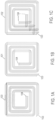
- FIG. 2 is an example of a non-self-resonating coil structure including an outer-edge fed, double-sided, printed circuit board, resonant induction wireless power transfer coil having 3 1 ⁇ 4 turns configured as a square, flat, planar spiral. the wireless power transfer coil may have at least 2 turns.
- FIG. 2A shows the top side conductor pattern 200 comprised of four independent conductors, although two or more independent conductors may be used.
- FIG. 2B shows the bottom side conductor pattern 201 as seen looking through the printed circuit board.
- the bottom side conductor pattern 201 is the same as the top side conductor pattern flipped left to right along the vertical centerline and rotated 90 degrees clockwise. It will be appreciated that the conductor patterns 200, 201 do not need to be identical and flipped.
- FIG. 2A shows the top side conductor pattern 200 comprised of four independent conductors, although two or more independent conductors may be used.
- FIG. 2B shows the bottom side conductor pattern 201 as seen looking through the printed circuit board.
- the number of traces operated in parallel to constitute a single winding conductor is determined by the operating frequency, the trace material conductivity, and the operating current.
- Narrow trace widths limit conductor eddy currents in the trace width dimensions and also maintain uniform current density across the individual trace cross-sections.
- Trace thickness is limited by the skin depth at the operating frequency as it contributes to AC resistance.
- top side conductor pattern 200 The longer outer conductors of the top side conductor pattern 200 are connected to the shorter inside conductors of the bottom side conductor pattern 201. Swapping conductors from inside to outside in this fashion equalizes conductor length and inductance. Equalized length and inductance equalizes resistance and reactance, which equalizes current distribution between conductors. Top side and bottom side conductors are superimposed. Magnetic flux flows through the inter-conductor gaps. In certain arrangements, all conductor traces are of equal length.
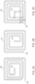
- FIG. 3 is a representation of a multi-layer, multi-conductor pair, edge terminated coil.
- FIG. 3 depicts an eight-layer stack up of individual coils that are roughly 3 1 ⁇ 4 to 3 1 ⁇ 2 turns each.
- Conductor pattern 300 is the top layer (layer 1), 301 is layer 2, 302 is layer 3, 303 is layer 4, 304 is layer 5, 305 is layer 6, 306 is layer 7, and 307 is the bottom layer (layer 8).
- Conductor pairs 300 and 301, 302 and 303, 304 and 305, 306 and 307 follow the same criteria as depicted in FIG. 2 .
- Coil terminals 104 of FIGS. 3A, 3C, 3E, and 3G receive input signals and coil terminals 104 of FIGS.
- FIG. 3I is the composite eight-layer stack up looking through the printed circuit board or laminate assembly from the top side.
- Conductor pattern 308 is the superposition of patterns 300-307.
- plated through holes 103 pass current between layers.
- Coil terminals 104 all lie on the outer edge of the coil assembly.
- an opening in the center of the coil structure may be provided that would allow current to be passed between layer pairs by means of an electrically conductive clamping mechanism.
- the coil stack of FIG. 3 may be provided within a multi-laminated assembly that could be implemented as a printed circuit board (PCB).
- PCB printed circuit board
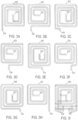
- FIG. 4 shows a cross-sectional view of four sample multi-layer coil stacks comprising 2n layers, where "n" can be any positive integer.
- the conductor patterns depicted in FIGS. 1 , 2 and 3 can apply to the cross-sections depicted in FIG. 4 .
- the arrangement of FIG. 4B is essentially a stack-up of two, two-layer panels depicted in FIG. 4A with an additional differential mode dielectric layer 402 in between.
- This implementation includes alternating forward and return current path conductors.
- the pattern 404 which includes a differential mode dielectric 402, forward current path conductor 400, a differential mode dielectric 402, and return current path conductor 401 is repeated.
- 401 the return current path conductor
- 402 the differential mode dielectric
- 403 a common mode dielectric layer.
- This configuration is similar to FIG. 4B except that the bottom two layers are inverted, such that the forward currents travel on the top and bottom layers 400 and the return currents travel on the inner layers 401.
- This configuration is similar to FIG. 4A , except that the top and bottom layers each have an additional layer added in parallel for carrying the forward and reverse currents. This results in common mode dielectrics 403 between the top two conductors 400 and bottom two conductors 401 and one differential mode dielectric 402 in the center of the four-layer stack-up.
- the pattern 406 on the top side which includes a common mode dielectric 403, and a forward current path conductor 400 is repeated.
- the pattern 407 on the bottom side which includes a common mode dielectric 403, and a reverse current path conductor 401, is repeated.
- FIGS. 4A through 4D may be used in the creation of other arrangements of more coil layers.
- six differential pairs of coil assemblies may be implemented as multiple instances and combinations of 4-layer stack-ups as depicted in FIGS. 4B, 4C, and 4D to provide a 24-layer coil design.
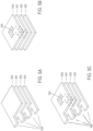
- FIG. 5 depicts perspective views for coil stacks that may be constructed of multiple, independent, multi-layer coil implementations as shown in FIGS. 1-4 .
- FIG. 5A is a physical representation of an edge-terminated coil stack that may be constructed of multiple, independent, multi-layer coil implementations as depicted in FIGS. 1-4 .
- four independent planar coils are provided that implement the conductor patterns of FIG. 3 .
- Item 500 is a planar coil that includes n layers of conductor patterns 300 and 301, where n is a positive integer.
- Item 501 is a planar coil that includes n layers of conductor patterns 302 and 303.
- Item 502 is a planar coil that includes n layers of conductor patterns 304 and 305.
- Item 503 is a planar coil that includes n layers of conductor patterns 306 and 307.
- Coil terminals 504 may be implemented as independent "tabs" of planar coils 500-503 that are offset along the edge to facilitate connection to independent terminal pairs as illustrated.
- the signals may pass between layers using vias or terminals connecting the boards through the middle as in the arrangements illustrated in FIGS. 1-4 .
- an edge pattern, spiraling from the edge inward, is provided and the boards pass signals through vias or terminals (not shown) connecting through the middle of the respective boards.
- FIG. 5B is a physical representation of a center-fed coil stack that may be constructed of multiple, independent, multi-layer coil implementations as depicted in FIGS. 1-4 .
- Item 500 is a planar coil that includes n layers of conductor patterns 300 and 301, wherein n is a positive integer.
- Item 501 is a planar coil that includes n layers of conductor patterns 302 and 303.
- Item 502 is a planar coil that includes n layers of conductor patterns 304 and 305.
- Item 503 is a planar coil that includes n layers of conductor patterns 306 and 307.
- Coil terminals 504 may be implemented as independent "tabs" of planar coils 500-503 that are offset along the center core to facilitate connection to independent terminal pairs as illustrated.
- the signals may pass between layers using vias or terminals connecting the boards through the middle as in the arrangements illustrated in FIGS. 1-4 .
- a center-fed pattern, spiraling from the center outward, is provided and the boards pass signals through vias or terminals (not shown) connecting through an outer corner of the respective boards.
- FIG. 5C is a physical representation of a coil stack that has both edge-terminations and center-terminations. Each coil stack may be constructed of multiple, independent, multi-layer coil implementations as depicted in FIGS. 1-4 .
- Item 500 is a planar coil that includes n layers of conductor patterns 300 and 301, where n is a positive integer.
- Item 501 is a planar coil that includes n layers of conductor patterns 302 and 303.
- Item 502 is a planar coil that includes n layers of conductor patterns 304 and 305.
- Item 503 is a planar coil that includes n layers of conductor patterns 306 and 307.
- Coil terminals 504 may be implemented as independent "tabs" of planar coils 500-503 that are offset along the edge and along the center core to facilitate connection to independent terminal pairs as illustrated.
- the signals may pass between layers using vias or terminals connecting the boards through the middle as in the arrangements illustrated in FIGS. 1-4 .
- the coil stack can be configured to be either an edge-fed or center-fed coil stack.
- Utilizing multiple, independent, multi-layer coil stacks as illustrated in FIG. 5 may provide cost benefits in manufacturing where the total number of coil conductor layers is large. Rather than producing one printed circuit board of 16 to 24 layers, for example, four to six 4-layer coil stacks may be integrated into one assembly. Additional arrangements could include "m" coil stacks, wherein "m” is any positive integer greater than one (e.g., two coil stacks with two tabs or ten coil stacks with ten tabs).
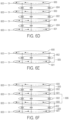
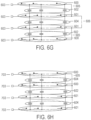
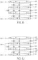
- FIG. 6 is the electrical form for the multi-layer, planar coil stack-ups that are depicted in FIG. 4 .
- FIGS. 6A, 6B, 6C , 6D , and 6I are unterminated and thus do not have direct electrical connections between layers in accordance with embodiments of the invention, while FIGS. 6E, 6F , 6G, 6H , and 6J are terminated and have serial and/or parallel connections between layers, depending on the configuration and, as such, do not fall within the scope of the invention.
Landscapes
- Engineering & Computer Science (AREA)
- Power Engineering (AREA)
- Computer Networks & Wireless Communication (AREA)
- Signal Processing (AREA)
- Coils Or Transformers For Communication (AREA)
- Coils Of Transformers For General Uses (AREA)
- Parts Printed On Printed Circuit Boards (AREA)
- Shielding Devices Or Components To Electric Or Magnetic Fields (AREA)
Priority Applications (1)
| Application Number | Priority Date | Filing Date | Title |
|---|---|---|---|
| EP24200840.7A EP4459887A3 (en) | 2017-05-30 | 2018-05-30 | Wireless power transfer thin profile coil assembly |
Applications Claiming Priority (3)
| Application Number | Priority Date | Filing Date | Title |
|---|---|---|---|
| US201762512544P | 2017-05-30 | 2017-05-30 | |
| EP18810537.3A EP3631819B1 (en) | 2017-05-30 | 2018-05-30 | Wireless power transfer thin profile coil assembly |
| PCT/US2018/035060 WO2018222669A1 (en) | 2017-05-30 | 2018-05-30 | Wireless power transfer thin profile coil assembly |
Related Parent Applications (2)
| Application Number | Title | Priority Date | Filing Date |
|---|---|---|---|
| EP18810537.3A Division-Into EP3631819B1 (en) | 2017-05-30 | 2018-05-30 | Wireless power transfer thin profile coil assembly |
| EP18810537.3A Division EP3631819B1 (en) | 2017-05-30 | 2018-05-30 | Wireless power transfer thin profile coil assembly |
Related Child Applications (2)
| Application Number | Title | Priority Date | Filing Date |
|---|---|---|---|
| EP24200840.7A Division EP4459887A3 (en) | 2017-05-30 | 2018-05-30 | Wireless power transfer thin profile coil assembly |
| EP24200840.7A Division-Into EP4459887A3 (en) | 2017-05-30 | 2018-05-30 | Wireless power transfer thin profile coil assembly |
Publications (3)
| Publication Number | Publication Date |
|---|---|
| EP3968346A1 EP3968346A1 (en) | 2022-03-16 |
| EP3968346C0 EP3968346C0 (en) | 2024-12-18 |
| EP3968346B1 true EP3968346B1 (en) | 2024-12-18 |
Family
ID=64456463
Family Applications (3)
| Application Number | Title | Priority Date | Filing Date |
|---|---|---|---|
| EP21203177.7A Active EP3968346B1 (en) | 2017-05-30 | 2018-05-30 | Wireless power transfer thin profile coil assembly |
| EP18810537.3A Active EP3631819B1 (en) | 2017-05-30 | 2018-05-30 | Wireless power transfer thin profile coil assembly |
| EP24200840.7A Pending EP4459887A3 (en) | 2017-05-30 | 2018-05-30 | Wireless power transfer thin profile coil assembly |
Family Applications After (2)
| Application Number | Title | Priority Date | Filing Date |
|---|---|---|---|
| EP18810537.3A Active EP3631819B1 (en) | 2017-05-30 | 2018-05-30 | Wireless power transfer thin profile coil assembly |
| EP24200840.7A Pending EP4459887A3 (en) | 2017-05-30 | 2018-05-30 | Wireless power transfer thin profile coil assembly |
Country Status (9)
| Country | Link |
|---|---|
| US (2) | US12159745B2 (enExample) |
| EP (3) | EP3968346B1 (enExample) |
| JP (2) | JP7082775B2 (enExample) |
| KR (1) | KR102405652B1 (enExample) |
| CN (1) | CN110999028B (enExample) |
| CA (1) | CA3065782A1 (enExample) |
| ES (2) | ES3010359T3 (enExample) |
| PT (1) | PT3631819T (enExample) |
| WO (1) | WO2018222669A1 (enExample) |
Families Citing this family (34)
| Publication number | Priority date | Publication date | Assignee | Title |
|---|---|---|---|---|
| CA3065782A1 (en) | 2017-05-30 | 2018-12-06 | Momentum Dynamics Corporation | Wireless power transfer thin profile coil assembly |
| JP2020027813A (ja) * | 2018-08-09 | 2020-02-20 | 矢崎総業株式会社 | 電力伝送ユニット |
| US12249847B2 (en) | 2018-12-31 | 2025-03-11 | 3M Innovative Properties Company | Wireless power transfer |
| WO2021059285A1 (en) * | 2019-09-26 | 2021-04-01 | Soreq Nuclear Research Center | Wireless enhanced power transfer |
| US11387678B2 (en) | 2019-09-27 | 2022-07-12 | Apple Inc. | Stacked resonant structures for wireless power systems |
| JP7619757B2 (ja) * | 2019-12-09 | 2025-01-22 | 三菱重工業株式会社 | 信号伝送回路 |
| TWI775022B (zh) * | 2019-12-16 | 2022-08-21 | 圓凱科技實業股份有限公司 | 可無線充電的墊體及其製法 |
| EP4117770A1 (en) | 2020-03-10 | 2023-01-18 | Tc1 Llc | Systems and methods for wireless energy transfer for ventricular assist devices |
| US12174269B2 (en) | 2020-03-20 | 2024-12-24 | InductEV, Inc. | Current sensing in a wireless power transfer system |
| US11784503B2 (en) | 2021-02-22 | 2023-10-10 | Inductev Inc. | Passive arc detection and mitigation in wireless power transfer system |
| US11585836B2 (en) | 2020-03-20 | 2023-02-21 | InductEV, Inc. | Current sensing in a wireless power transfer system |
| CN113539636B (zh) * | 2020-04-13 | 2022-12-06 | 鹏鼎控股(深圳)股份有限公司 | 无线充电线圈结构及其制备方法 |
| US11581755B2 (en) * | 2020-07-28 | 2023-02-14 | InductEV, Inc. | Efficiency gains through magnetic field management |
| KR102544750B1 (ko) * | 2020-12-22 | 2023-06-16 | 주식회사 유라코퍼레이션 | 무선충전시스템 |
| CN113192721A (zh) * | 2021-01-21 | 2021-07-30 | 龙腾 | 基于印制电路板的电感结构、包含该结构的柔性多层印制电路板及包含该结构的变压器结构 |
| DE102021112455A1 (de) * | 2021-05-12 | 2022-11-17 | Technische Universität Dresden, Körperschaft des öffentlichen Rechts | Spulenanordnungen und Verfahren zum Herstellen einer Spulenanordnung |
| EP4356406A4 (en) | 2021-06-16 | 2025-04-16 | Resonant Link, Inc. | High efficiency wireless power transfer coils |
| US20240283293A1 (en) * | 2021-06-18 | 2024-08-22 | Hyundai Motor Company | Wireless power transfer device comprising coil structure and power transfer circuit for wireless power transfer, and wireless power reception device |
| US20240425304A1 (en) * | 2021-11-05 | 2024-12-26 | Siemens Healthcare Diagnostics Inc. | Electromagnetic pcb crossroads topologies for automation track systems |
| CN114496502B (zh) * | 2021-12-28 | 2025-08-19 | 中兴新能源科技有限公司 | 一种线圈绕制结构、线圈绕制方法及变压器 |
| US12145461B2 (en) | 2022-01-06 | 2024-11-19 | Ev Charging Solutions, Llc | Inductive charging station |
| US20240006916A1 (en) * | 2022-07-01 | 2024-01-04 | Toyota Motor Engineering & Manufacturing North America, Inc. | Modular pcb-based coil for ev wireless charging with thermally conductive separator |
| TWI801302B (zh) * | 2022-08-11 | 2023-05-01 | 台灣電力股份有限公司 | 用於無線電力裝置之頻率選擇表面結構 |
| KR102540173B1 (ko) * | 2022-09-14 | 2023-06-07 | 주식회사 스키아 | Mr영상을 이용한 유방영역 분할 장치 및 방법 |
| KR20240038433A (ko) * | 2022-09-16 | 2024-03-25 | 주식회사 모다이노칩 | 전자 부품 |
| CN120548667A (zh) * | 2023-01-13 | 2025-08-26 | 南洋理工大学 | 印刷电路板谐振器及其制造方法 |
| WO2024197687A1 (en) * | 2023-03-30 | 2024-10-03 | Renesas Electronics America Inc. | Hybrid coil for wireless power transfer |
| CN116469654B (zh) * | 2023-04-04 | 2024-05-14 | 深圳市德维斯电子有限公司 | 一种变压器结构及其组立助装件 |
| JPWO2024241842A1 (enExample) * | 2023-05-22 | 2024-11-28 | ||
| DE102023126454A1 (de) * | 2023-09-28 | 2025-04-03 | Universität Stuttgart, Körperschaft Des Öffentlichen Rechts | Elektrische Leitung, Spule und induktive Energieübertragungsvorrichtung |
| US20250118476A1 (en) * | 2023-10-05 | 2025-04-10 | Delta Electronics, Inc. | Flex pcb winding with thermal cooling |
| KR102698083B1 (ko) * | 2024-03-15 | 2024-08-23 | 주식회사 지성전자 | 용량조절이 가능한 적층형 무선충전모듈 |
| WO2025192971A1 (ko) * | 2024-03-15 | 2025-09-18 | 엘지이노텍 주식회사 | 다층 구조를 갖는 코일의 각 층 또는 복수의 코일 소자 간의 연결을 직렬 방식 또는 병렬 방식으로 선택적으로 연결할 수 있는 코일 구조를 갖는 충전기 및 코일 구조 |
| WO2025192970A1 (ko) * | 2024-03-15 | 2025-09-18 | 엘지이노텍 주식회사 | 전기차 무선 충전 시스템의 동적 위상 제어를 위한 송신 코일 구조를 갖는 충전기 및 동적 위상 제어를 위한 코일 구조 |
Family Cites Families (45)
| Publication number | Priority date | Publication date | Assignee | Title |
|---|---|---|---|---|
| US20030161086A1 (en) | 2000-07-18 | 2003-08-28 | X2Y Attenuators, Llc | Paired multi-layered dielectric independent passive component architecture resulting in differential and common mode filtering with surge protection in one integrated package |
| US8169185B2 (en) * | 2006-01-31 | 2012-05-01 | Mojo Mobility, Inc. | System and method for inductive charging of portable devices |
| US7973635B2 (en) * | 2007-09-28 | 2011-07-05 | Access Business Group International Llc | Printed circuit board coil |
| US20100261038A1 (en) * | 2007-11-02 | 2010-10-14 | Nobuyoshi Imaoka | Composite magnetic material for magnet and method for manufacturing such material |
| JP2012527813A (ja) * | 2009-05-20 | 2012-11-08 | コーニンクレッカ フィリップス エレクトロニクス エヌ ヴィ | 超薄遮蔽層をもつ誘導型受信コイルを有する電子装置及び方法 |
| CN103401321B (zh) * | 2009-06-25 | 2016-05-25 | 株式会社村田制作所 | 功率传送系统和非接触充电装置 |
| CN102474009B (zh) * | 2009-07-03 | 2015-01-07 | 株式会社村田制作所 | 天线及天线模块 |
| JP5471283B2 (ja) * | 2009-10-19 | 2014-04-16 | Tdk株式会社 | ワイヤレス給電装置、ワイヤレス受電装置およびワイヤレス電力伝送システム |
| US8551163B2 (en) | 2010-10-07 | 2013-10-08 | Everheart Systems Inc. | Cardiac support systems and methods for chronic use |
| WO2012053439A1 (ja) * | 2010-10-21 | 2012-04-26 | Tdk株式会社 | コイル部品及びその製造方法 |
| KR101896631B1 (ko) | 2010-12-01 | 2018-09-07 | 파나소닉 주식회사 | 비접촉 충전모듈 및 비접촉 충전기기 |
| JP5838562B2 (ja) * | 2011-02-17 | 2016-01-06 | 富士通株式会社 | ワイヤレス送電装置及びワイヤレス送電システム |
| US8970069B2 (en) * | 2011-03-28 | 2015-03-03 | Tdk Corporation | Wireless power receiver and wireless power transmission system |
| US20120274148A1 (en) * | 2011-04-27 | 2012-11-01 | Samsung Electro-Mechanics Co., Ltd. | Contactless power transmission device and electronic device having the same |
| JP2013062386A (ja) * | 2011-09-14 | 2013-04-04 | Tokai Rubber Ind Ltd | 無接点電力伝送装置 |
| US9240270B2 (en) * | 2011-10-07 | 2016-01-19 | Utah State University | Wireless power transfer magnetic couplers |
| US9160205B2 (en) * | 2012-03-20 | 2015-10-13 | Qualcomm Incorporated | Magnetically permeable structures |
| KR101339486B1 (ko) * | 2012-03-29 | 2013-12-10 | 삼성전기주식회사 | 박막 코일 및 이를 구비하는 전자 기기 |
| JP6083652B2 (ja) | 2012-05-28 | 2017-02-22 | パナソニックIpマネジメント株式会社 | 無接点コネクタシステム |
| US9931952B2 (en) | 2012-06-27 | 2018-04-03 | Qualcomm Incorporated | Electric vehicle wireless charging with monitoring of duration of charging operational mode |
| US20140177197A1 (en) * | 2012-12-26 | 2014-06-26 | Nokia Corporation | Multi-Layered Magnetic Shields |
| WO2014130065A1 (en) * | 2013-02-25 | 2014-08-28 | Access Business Group International Llc | Variable pitch spiral coil |
| KR101703842B1 (ko) * | 2013-03-05 | 2017-02-08 | 주식회사 아모센스 | 자기장 및 전자파 차폐용 복합시트 및 이를 구비하는 안테나 모듈 |
| CN105431916B (zh) | 2013-03-27 | 2018-08-17 | 奥克兰联合服务有限公司 | 电磁场限制 |
| JP6306288B2 (ja) | 2013-05-13 | 2018-04-04 | 日東電工株式会社 | コイルプリント配線基板、受電モジュール、電池ユニットおよび受電通信モジュール |
| CN104184217B (zh) * | 2013-08-21 | 2016-08-10 | 深圳市安普盛科技有限公司 | 用于无线电能传输的感应线圈及制造方法、无线充电系统 |
| US20150077208A1 (en) * | 2013-09-16 | 2015-03-19 | Ken Goldman | High-q parallel-trace planar spiral coil for biomedical implants |
| US20160276079A1 (en) | 2013-11-01 | 2016-09-22 | Toda Kogyo Corp. | Soft magnetic ferrite resin composition, soft magnetic ferrite resin composition molded product, and power transmission device for non-contact power feeder system |
| EP3069358B1 (en) * | 2013-11-11 | 2019-06-12 | Tc1 Llc | Hinged resonant power transfer coil |
| EP3134956A4 (en) * | 2014-04-16 | 2018-01-24 | Witricity Corporation | Wireless energy transfer for mobile device applications |
| JP6332002B2 (ja) * | 2014-11-01 | 2018-05-30 | パナソニックIpマネジメント株式会社 | 送電装置、送電装置を搭載した車両及び無線電力伝送システム |
| CN105576847B (zh) * | 2014-11-01 | 2018-05-11 | 松下知识产权经营株式会社 | 送电装置、搭载有送电装置的车辆以及无线电力传输系统 |
| US10332672B2 (en) * | 2015-01-12 | 2019-06-25 | Amogreentech Co., Ltd. | Heat radiation unit and wireless power transmitting and receiving device having same |
| US9912172B2 (en) * | 2015-01-14 | 2018-03-06 | Qualcomm Incorporated | Asymmetrically layered stacked coils and/or chamfered ferrite in wireless power transfer applications |
| JP6596942B2 (ja) | 2015-06-04 | 2019-10-30 | 株式会社Ihi | コイル装置 |
| US10320586B2 (en) | 2015-07-14 | 2019-06-11 | At&T Intellectual Property I, L.P. | Apparatus and methods for generating non-interfering electromagnetic waves on an insulated transmission medium |
| KR101926594B1 (ko) | 2015-08-20 | 2018-12-10 | 주식회사 아모텍 | 무선충전형 안테나유닛 및 이를 포함하는 무선전력 충전모듈 |
| KR102405414B1 (ko) * | 2015-10-13 | 2022-06-07 | 주식회사 위츠 | 자기장 차폐 시트 및 이를 포함하는 무선 충전 장치 |
| US9899879B2 (en) * | 2016-02-15 | 2018-02-20 | Motorola Solutions, Inc. | Systems and methods for controlling wireless power transfer |
| JP6743432B2 (ja) * | 2016-03-14 | 2020-08-19 | 株式会社Ihi | コイル装置 |
| US10374467B2 (en) * | 2016-03-30 | 2019-08-06 | Tdk Corporation | Coil unit, wireless power feeding device, wireless power receiving device and wireless power transmission device |
| KR101772871B1 (ko) * | 2016-07-11 | 2017-08-30 | 주식회사 두산 | 안테나 모듈 형성용 복합기판 및 이의 제조방법 |
| TW201816539A (zh) * | 2016-10-20 | 2018-05-01 | 華碩電腦股份有限公司 | 無線充電結構及其製造方法 |
| CN110383404B (zh) * | 2017-03-10 | 2022-05-17 | 三菱电机工程技术株式会社 | 谐振型电力传输用线圈 |
| CA3065782A1 (en) | 2017-05-30 | 2018-12-06 | Momentum Dynamics Corporation | Wireless power transfer thin profile coil assembly |
-
2018
- 2018-05-30 CA CA3065782A patent/CA3065782A1/en active Pending
- 2018-05-30 EP EP21203177.7A patent/EP3968346B1/en active Active
- 2018-05-30 CN CN201880035909.7A patent/CN110999028B/zh active Active
- 2018-05-30 US US16/615,290 patent/US12159745B2/en active Active
- 2018-05-30 ES ES21203177T patent/ES3010359T3/es active Active
- 2018-05-30 PT PT188105373T patent/PT3631819T/pt unknown
- 2018-05-30 EP EP18810537.3A patent/EP3631819B1/en active Active
- 2018-05-30 ES ES18810537T patent/ES2964226T3/es active Active
- 2018-05-30 JP JP2019565876A patent/JP7082775B2/ja active Active
- 2018-05-30 EP EP24200840.7A patent/EP4459887A3/en active Pending
- 2018-05-30 WO PCT/US2018/035060 patent/WO2018222669A1/en not_active Ceased
- 2018-05-30 KR KR1020197038173A patent/KR102405652B1/ko active Active
-
2022
- 2022-04-21 JP JP2022069788A patent/JP7350382B2/ja active Active
-
2024
- 2024-10-27 US US18/928,155 patent/US20250095912A1/en active Pending
Also Published As
| Publication number | Publication date |
|---|---|
| ES3010359T3 (en) | 2025-04-02 |
| WO2018222669A1 (en) | 2018-12-06 |
| JP2022115872A (ja) | 2022-08-09 |
| EP3631819B1 (en) | 2023-10-18 |
| EP4459887A2 (en) | 2024-11-06 |
| JP7082775B2 (ja) | 2022-06-09 |
| CN110999028A (zh) | 2020-04-10 |
| JP2020522885A (ja) | 2020-07-30 |
| EP3968346A1 (en) | 2022-03-16 |
| EP3968346C0 (en) | 2024-12-18 |
| EP3631819A1 (en) | 2020-04-08 |
| KR102405652B1 (ko) | 2022-06-03 |
| CA3065782A1 (en) | 2018-12-06 |
| PT3631819T (pt) | 2023-10-27 |
| US12159745B2 (en) | 2024-12-03 |
| CN110999028B (zh) | 2023-11-21 |
| US20250095912A1 (en) | 2025-03-20 |
| EP4459887A3 (en) | 2025-01-22 |
| ES2964226T3 (es) | 2024-04-04 |
| EP3631819A4 (en) | 2021-06-02 |
| KR20200012916A (ko) | 2020-02-05 |
| US20200168393A1 (en) | 2020-05-28 |
| JP7350382B2 (ja) | 2023-09-26 |
Similar Documents
| Publication | Publication Date | Title |
|---|---|---|
| US20250095912A1 (en) | Wireless Power Transfer Thin Profile Coil Assembly | |
| JP2020522885A5 (enExample) | ||
| EP0388985B1 (en) | LC noise filter | |
| US11515084B2 (en) | Magnetic component and wireless power-transferring device including the same | |
| US20030095027A1 (en) | Planar printed circuit-board transformers with effective electromagnetic interference (EMI) shielding | |
| EP2546999A2 (en) | Wireless power transmitting device for wireless power communication system | |
| US20210193381A1 (en) | Series self-resonant coil structure for conducting wireless power transfer | |
| EP3771071A1 (en) | Wireless charging pad and wireless charging device | |
| WO2016190708A1 (ko) | 무선전력 전송용 안테나유닛 및 이를 포함하는 무선전력 송신모듈 | |
| JP5820515B2 (ja) | マルチトロイド変圧器 | |
| CN109524209A (zh) | 开关电源及小型变压器 | |
| CN210517814U (zh) | 一种应用于无线充电的中继系统及中继装置 | |
| EP3669389B1 (en) | Topology of a ferrite shield for inductive coils | |
| CN211720336U (zh) | 异物检测设备和无线充电系统 | |
| US10944292B2 (en) | Wireless power supply device | |
| KR102698083B1 (ko) | 용량조절이 가능한 적층형 무선충전모듈 | |
| KR102800020B1 (ko) | 플랫코일 및 이를 이용한 전원공급장치 | |
| WO2024197688A1 (en) | Split planar coil for wireless power transfer | |
| KR20210036303A (ko) | 다층 인덕터 | |
| KR20200052033A (ko) | 무선 충전 패드 및 무선 충전 장치 | |
| KR20150108439A (ko) | 동축형 교류케이블 |
Legal Events
| Date | Code | Title | Description |
|---|---|---|---|
| PUAI | Public reference made under article 153(3) epc to a published international application that has entered the european phase |
Free format text: ORIGINAL CODE: 0009012 |
|
| STAA | Information on the status of an ep patent application or granted ep patent |
Free format text: STATUS: THE APPLICATION HAS BEEN PUBLISHED |
|
| AC | Divisional application: reference to earlier application |
Ref document number: 3631819 Country of ref document: EP Kind code of ref document: P |
|
| AK | Designated contracting states |
Kind code of ref document: A1 Designated state(s): AL AT BE BG CH CY CZ DE DK EE ES FI FR GB GR HR HU IE IS IT LI LT LU LV MC MK MT NL NO PL PT RO RS SE SI SK SM TR |
|
| STAA | Information on the status of an ep patent application or granted ep patent |
Free format text: STATUS: REQUEST FOR EXAMINATION WAS MADE |
|
| 17P | Request for examination filed |
Effective date: 20220620 |
|
| RBV | Designated contracting states (corrected) |
Designated state(s): AL AT BE BG CH CY CZ DE DK EE ES FI FR GB GR HR HU IE IS IT LI LT LU LV MC MK MT NL NO PL PT RO RS SE SI SK SM TR |
|
| RAP3 | Party data changed (applicant data changed or rights of an application transferred) |
Owner name: INDUCTEV INC. |
|
| STAA | Information on the status of an ep patent application or granted ep patent |
Free format text: STATUS: EXAMINATION IS IN PROGRESS |
|
| 17Q | First examination report despatched |
Effective date: 20230421 |
|
| RIC1 | Information provided on ipc code assigned before grant |
Ipc: H04B 5/79 20240101ALI20240613BHEP Ipc: H01F 27/36 20060101ALI20240613BHEP Ipc: H01F 27/28 20060101ALI20240613BHEP Ipc: H01F 5/00 20060101ALI20240613BHEP Ipc: H01F 38/14 20060101AFI20240613BHEP |
|
| GRAP | Despatch of communication of intention to grant a patent |
Free format text: ORIGINAL CODE: EPIDOSNIGR1 |
|
| STAA | Information on the status of an ep patent application or granted ep patent |
Free format text: STATUS: GRANT OF PATENT IS INTENDED |
|
| INTG | Intention to grant announced |
Effective date: 20240719 |
|
| RAP3 | Party data changed (applicant data changed or rights of an application transferred) |
Owner name: INDUCTEV INC. |
|
| GRAS | Grant fee paid |
Free format text: ORIGINAL CODE: EPIDOSNIGR3 |
|
| GRAA | (expected) grant |
Free format text: ORIGINAL CODE: 0009210 |
|
| STAA | Information on the status of an ep patent application or granted ep patent |
Free format text: STATUS: THE PATENT HAS BEEN GRANTED |
|
| AC | Divisional application: reference to earlier application |
Ref document number: 3631819 Country of ref document: EP Kind code of ref document: P |
|
| AK | Designated contracting states |
Kind code of ref document: B1 Designated state(s): AL AT BE BG CH CY CZ DE DK EE ES FI FR GB GR HR HU IE IS IT LI LT LU LV MC MK MT NL NO PL PT RO RS SE SI SK SM TR |
|
| REG | Reference to a national code |
Ref country code: CH Ref legal event code: EP |
|
| REG | Reference to a national code |
Ref country code: DE Ref legal event code: R096 Ref document number: 602018077851 Country of ref document: DE |
|
| REG | Reference to a national code |
Ref country code: IE Ref legal event code: FG4D |
|
| U01 | Request for unitary effect filed |
Effective date: 20250102 |
|
| U07 | Unitary effect registered |
Designated state(s): AT BE BG DE DK EE FI FR IT LT LU LV MT NL PT RO SE SI Effective date: 20250114 |
|
| REG | Reference to a national code |
Ref country code: ES Ref legal event code: FG2A Ref document number: 3010359 Country of ref document: ES Kind code of ref document: T3 Effective date: 20250402 |
|
| PG25 | Lapsed in a contracting state [announced via postgrant information from national office to epo] |
Ref country code: HR Free format text: LAPSE BECAUSE OF FAILURE TO SUBMIT A TRANSLATION OF THE DESCRIPTION OR TO PAY THE FEE WITHIN THE PRESCRIBED TIME-LIMIT Effective date: 20241218 |
|
| PG25 | Lapsed in a contracting state [announced via postgrant information from national office to epo] |
Ref country code: NO Free format text: LAPSE BECAUSE OF FAILURE TO SUBMIT A TRANSLATION OF THE DESCRIPTION OR TO PAY THE FEE WITHIN THE PRESCRIBED TIME-LIMIT Effective date: 20250318 |
|
| PG25 | Lapsed in a contracting state [announced via postgrant information from national office to epo] |
Ref country code: GR Free format text: LAPSE BECAUSE OF FAILURE TO SUBMIT A TRANSLATION OF THE DESCRIPTION OR TO PAY THE FEE WITHIN THE PRESCRIBED TIME-LIMIT Effective date: 20250319 |
|
| PG25 | Lapsed in a contracting state [announced via postgrant information from national office to epo] |
Ref country code: RS Free format text: LAPSE BECAUSE OF FAILURE TO SUBMIT A TRANSLATION OF THE DESCRIPTION OR TO PAY THE FEE WITHIN THE PRESCRIBED TIME-LIMIT Effective date: 20250318 |
|
| U20 | Renewal fee for the european patent with unitary effect paid |
Year of fee payment: 8 Effective date: 20250430 |
|
| PG25 | Lapsed in a contracting state [announced via postgrant information from national office to epo] |
Ref country code: SM Free format text: LAPSE BECAUSE OF FAILURE TO SUBMIT A TRANSLATION OF THE DESCRIPTION OR TO PAY THE FEE WITHIN THE PRESCRIBED TIME-LIMIT Effective date: 20241218 |
|
| PG25 | Lapsed in a contracting state [announced via postgrant information from national office to epo] |
Ref country code: PL Free format text: LAPSE BECAUSE OF FAILURE TO SUBMIT A TRANSLATION OF THE DESCRIPTION OR TO PAY THE FEE WITHIN THE PRESCRIBED TIME-LIMIT Effective date: 20241218 |
|
| PGFP | Annual fee paid to national office [announced via postgrant information from national office to epo] |
Ref country code: GB Payment date: 20250429 Year of fee payment: 8 Ref country code: ES Payment date: 20250606 Year of fee payment: 8 |
|
| PG25 | Lapsed in a contracting state [announced via postgrant information from national office to epo] |
Ref country code: IS Free format text: LAPSE BECAUSE OF FAILURE TO SUBMIT A TRANSLATION OF THE DESCRIPTION OR TO PAY THE FEE WITHIN THE PRESCRIBED TIME-LIMIT Effective date: 20250418 |
|
| PG25 | Lapsed in a contracting state [announced via postgrant information from national office to epo] |
Ref country code: SK Free format text: LAPSE BECAUSE OF FAILURE TO SUBMIT A TRANSLATION OF THE DESCRIPTION OR TO PAY THE FEE WITHIN THE PRESCRIBED TIME-LIMIT Effective date: 20241218 |
|
| PG25 | Lapsed in a contracting state [announced via postgrant information from national office to epo] |
Ref country code: CZ Free format text: LAPSE BECAUSE OF FAILURE TO SUBMIT A TRANSLATION OF THE DESCRIPTION OR TO PAY THE FEE WITHIN THE PRESCRIBED TIME-LIMIT Effective date: 20241218 |
|
| PLBE | No opposition filed within time limit |
Free format text: ORIGINAL CODE: 0009261 |
|
| STAA | Information on the status of an ep patent application or granted ep patent |
Free format text: STATUS: NO OPPOSITION FILED WITHIN TIME LIMIT |
|
| 26N | No opposition filed |
Effective date: 20250919 |