EP3965541A1 - Housing and electronic device - Google Patents
Housing and electronic device Download PDFInfo
- Publication number
- EP3965541A1 EP3965541A1 EP20822550.8A EP20822550A EP3965541A1 EP 3965541 A1 EP3965541 A1 EP 3965541A1 EP 20822550 A EP20822550 A EP 20822550A EP 3965541 A1 EP3965541 A1 EP 3965541A1
- Authority
- EP
- European Patent Office
- Prior art keywords
- receiving area
- electronic component
- electronic device
- heat
- housing
- Prior art date
- Legal status (The legal status is an assumption and is not a legal conclusion. Google has not performed a legal analysis and makes no representation as to the accuracy of the status listed.)
- Withdrawn
Links
- 230000001681 protective effect Effects 0.000 claims abstract description 64
- 230000017525 heat dissipation Effects 0.000 claims abstract description 31
- 239000010410 layer Substances 0.000 claims description 13
- OKTJSMMVPCPJKN-UHFFFAOYSA-N Carbon Chemical compound [C] OKTJSMMVPCPJKN-UHFFFAOYSA-N 0.000 claims description 6
- 229910002804 graphite Inorganic materials 0.000 claims description 6
- 239000010439 graphite Substances 0.000 claims description 6
- 239000012790 adhesive layer Substances 0.000 claims description 5
- 239000002184 metal Substances 0.000 claims description 5
- 229910052751 metal Inorganic materials 0.000 claims description 5
- 238000012545 processing Methods 0.000 claims description 5
- 238000004891 communication Methods 0.000 abstract description 7
- 238000013021 overheating Methods 0.000 abstract description 6
- 238000010438 heat treatment Methods 0.000 abstract description 2
- 239000012071 phase Substances 0.000 description 8
- 239000007791 liquid phase Substances 0.000 description 6
- 239000000463 material Substances 0.000 description 6
- RYGMFSIKBFXOCR-UHFFFAOYSA-N Copper Chemical compound [Cu] RYGMFSIKBFXOCR-UHFFFAOYSA-N 0.000 description 5
- 238000009833 condensation Methods 0.000 description 5
- 230000005494 condensation Effects 0.000 description 5
- 238000001704 evaporation Methods 0.000 description 5
- 230000008020 evaporation Effects 0.000 description 5
- 238000000034 method Methods 0.000 description 5
- 239000011889 copper foil Substances 0.000 description 4
- 238000010586 diagram Methods 0.000 description 4
- 230000008569 process Effects 0.000 description 4
- 238000012546 transfer Methods 0.000 description 4
- 230000001413 cellular effect Effects 0.000 description 3
- 230000000694 effects Effects 0.000 description 3
- 238000011160 research Methods 0.000 description 3
- XEEYBQQBJWHFJM-UHFFFAOYSA-N Iron Chemical compound [Fe] XEEYBQQBJWHFJM-UHFFFAOYSA-N 0.000 description 2
- 238000012986 modification Methods 0.000 description 2
- 230000004048 modification Effects 0.000 description 2
- 239000000853 adhesive Substances 0.000 description 1
- 230000001070 adhesive effect Effects 0.000 description 1
- 150000001298 alcohols Chemical class 0.000 description 1
- 229910052802 copper Inorganic materials 0.000 description 1
- 239000010949 copper Substances 0.000 description 1
- 238000013461 design Methods 0.000 description 1
- 238000001514 detection method Methods 0.000 description 1
- 238000011161 development Methods 0.000 description 1
- 238000004512 die casting Methods 0.000 description 1
- 238000006073 displacement reaction Methods 0.000 description 1
- 238000005530 etching Methods 0.000 description 1
- 239000003292 glue Substances 0.000 description 1
- 230000006872 improvement Effects 0.000 description 1
- 238000009434 installation Methods 0.000 description 1
- 229910052742 iron Inorganic materials 0.000 description 1
- 238000002955 isolation Methods 0.000 description 1
- 230000007257 malfunction Effects 0.000 description 1
- 239000011148 porous material Substances 0.000 description 1
- 238000000926 separation method Methods 0.000 description 1
- 238000005245 sintering Methods 0.000 description 1
- 230000007480 spreading Effects 0.000 description 1
- 238000012360 testing method Methods 0.000 description 1
- XLYOFNOQVPJJNP-UHFFFAOYSA-N water Substances O XLYOFNOQVPJJNP-UHFFFAOYSA-N 0.000 description 1
Images


Classifications
-
- H—ELECTRICITY
- H05—ELECTRIC TECHNIQUES NOT OTHERWISE PROVIDED FOR
- H05K—PRINTED CIRCUITS; CASINGS OR CONSTRUCTIONAL DETAILS OF ELECTRIC APPARATUS; MANUFACTURE OF ASSEMBLAGES OF ELECTRICAL COMPONENTS
- H05K7/00—Constructional details common to different types of electric apparatus
- H05K7/20—Modifications to facilitate cooling, ventilating, or heating
- H05K7/2029—Modifications to facilitate cooling, ventilating, or heating using a liquid coolant with phase change in electronic enclosures
- H05K7/20336—Heat pipes, e.g. wicks or capillary pumps
-
- H—ELECTRICITY
- H05—ELECTRIC TECHNIQUES NOT OTHERWISE PROVIDED FOR
- H05K—PRINTED CIRCUITS; CASINGS OR CONSTRUCTIONAL DETAILS OF ELECTRIC APPARATUS; MANUFACTURE OF ASSEMBLAGES OF ELECTRICAL COMPONENTS
- H05K5/00—Casings, cabinets or drawers for electric apparatus
- H05K5/0086—Casings, cabinets or drawers for electric apparatus portable, e.g. battery operated apparatus
-
- H—ELECTRICITY
- H05—ELECTRIC TECHNIQUES NOT OTHERWISE PROVIDED FOR
- H05K—PRINTED CIRCUITS; CASINGS OR CONSTRUCTIONAL DETAILS OF ELECTRIC APPARATUS; MANUFACTURE OF ASSEMBLAGES OF ELECTRICAL COMPONENTS
- H05K7/00—Constructional details common to different types of electric apparatus
- H05K7/20—Modifications to facilitate cooling, ventilating, or heating
- H05K7/2039—Modifications to facilitate cooling, ventilating, or heating characterised by the heat transfer by conduction from the heat generating element to a dissipating body
- H05K7/20436—Inner thermal coupling elements in heat dissipating housings, e.g. protrusions or depressions integrally formed in the housing
-
- H—ELECTRICITY
- H05—ELECTRIC TECHNIQUES NOT OTHERWISE PROVIDED FOR
- H05K—PRINTED CIRCUITS; CASINGS OR CONSTRUCTIONAL DETAILS OF ELECTRIC APPARATUS; MANUFACTURE OF ASSEMBLAGES OF ELECTRICAL COMPONENTS
- H05K7/00—Constructional details common to different types of electric apparatus
- H05K7/20—Modifications to facilitate cooling, ventilating, or heating
- H05K7/20954—Modifications to facilitate cooling, ventilating, or heating for display panels
- H05K7/2099—Liquid coolant with phase change
Definitions
- the protective member is arranged opposite or in contact with the electronic component provided in the first receiving area.
- the heat generated by the first electronic component is transferred, through the protective member and the heat-conducting element, to other locations of the electronic device, and then is dissipated to the outside. Accordingly, the heat balance of the electronic device is achieved, and the local overheating of the electronic device is avoided, thereby improving the heat dissipation efficiency of the electronic device.
- the protective member it is possible to prevent the battery from being damaged by the heat-conducting element when the heat-conducting element is dislocated, thereby improving the reliability of the electronic device.
- the inventor continues to study how to prevent the dislocation of the heat pipe and thus protect the battery without changing the thickness of the electronic device, so as to realize the heat balance and heat dissipation of the electronic device, thereby improving the heat dissipation performance of the electronic device.
- the inventor has researched how to avoid the dislocation of the heat pipe in the electronic device, how to make the positions of the heat pipe and the battery relatively fixed, how to make the heat dissipation structure dissipate the heat rapidly in the electronic device, and so on.
- the inventor further conducted research on how to design a heat dissipation structure that enables heat balance in the electronic device, and thus proposed the technical solutions of the embodiments of the present disclosure.
- the electronic device 100 includes a housing 200, a display panel 130, a first electronic component 150, and a second electronic component 170.
- the housing 200 and the display panel 130 cooperatively define a receiving cavity, and the first electronic component 150 and the second electronic component 170 are accommodated in the receiving cavity.
- the housing 200 can provide protection for the first electronic component 150 and the second electronic component 170, to prevent the first electronic component 150 and the second electronic component 170 from being dislocated or damaged under the impact of an external force, thereby prolonging the service life of the electronic device 100.
- the protective member 250 is arranged opposite or in contact with the first electronic component 150 provided in the first receiving area 211. As such, the heat generated by the first electronic component 150 is transferred, through the protective member 250 and the heat-conducting element 230, to other locations of the electronic device 100, and then is dissipated to the outside. Accordingly, the heat balance of the electronic device 100 is achieved, and the local overheating of the electronic device 100 is avoided, thereby improving the heat dissipation efficiency of the electronic device 100.
- the middle frame 210 is configured to install or carry the first electronic component 150 and the second electronic component 170 to limit the positions of the first electronic component 150 and the second electronic component 170, thereby avoiding malfunction of the electronic device 100 from being caused by the displacement of the first electronic component150 and the second electronic component 170.
- the first surface 212 may serve as the bottom wall of the first receiving area 211 and the second receiving area 215, so that the first electronic component 150 received in the first receiving area 211 and the second electronic component 170 received in the second receiving area 215 are further confined.
- the first receiving area 211 and the second receiving area 215 may be located on opposite sides of the middle frame 210.
- the first receiving area 211 is provided on the first surface 212
- the second receiving area 215 is provided on the second surface 214.
- the protective member 250 is disposed in the accommodating groove 213, and spans across the first receiving area 211 and the second receiving area 215.
- the two opposite ends of the protective member 250 are respectively located at the first receiving area 211 and the second receiving area 215, to cover an opening formed by the accommodating groove 213 in the first receiving area 211 and an opening formed by the accommodating groove 213 in the second receiving area 215.
- the protective member includes two bent parts 253 respectively connected to opposite sides of the main body 251, and each of the two bent parts is superposed on a respective one of the two mounting parts 219, thereby improving the protection to the heat-conducting element 230. Further, by limiting the position of the protective member 250 through the two end surfaces 2191 of the two mounting parts 219, the protective member 250 can be prevented from shaking when the protective member 250 is accommodated in the accommodating groove 213.
- the heat-conducting element 230 is accommodated in the accommodating groove 213, and is disposed on a side of the protective member 250 that is away from the first electronic component 150.
- the heat-conducting element 230 is opposite to the main body 251, and the bent part 253 limits the position of the heat-conducting element 230.
- opposite ends of the heat-conducting element 230 are located at positions corresponding to the first receiving area 211 and the second receiving area 215, respectively, so that the heat-conducting element 230 can balance the heat of the first receiving area 211 and the heat of the second receiving area 215.
- the capillary layer 231 may be an independent element, for example, the capillary layer 231 is a metal weaved mesh which is connected to the inner surface of the heat-conducting element 230 by means of sintering or the like. Also optionally, the capillary layer 231 may be a tiny structure formed on the inner surface of the heat-conducting element 230 by etching or the like.
- the working process of the heat-conducting element 230 is explained by taking a case where an end of the heat-conducting element 230 close to the second electronic component 170 is an evaporation end, and an end thereof close to the first electronic component 150 is a condensation end, as an example.
- the working medium 233 in the liquid phase absorbs the heat and evaporates at the evaporation end, and becomes the working medium 233 in the gas phase to move and spread toward the condensation end.
Landscapes
- Engineering & Computer Science (AREA)
- Microelectronics & Electronic Packaging (AREA)
- Physics & Mathematics (AREA)
- Thermal Sciences (AREA)
- Cooling Or The Like Of Electrical Apparatus (AREA)
Abstract
Description
- This disclosure relates to the field of consumer electronics, and particularly to a housing and an electronic device.
- With the technological development of electronic devices, more and more electronic devices are involved in people's daily life. As the performance and functions of the electronic devices, such as mobile phones and tablets, are getting higher and higher, the heating problem of these electronic devices is becoming more and more serious.
- In the related electronic devices, the heat dissipation is mainly performed by adding a heat dispersing material with a good thermal conductivity, such as graphite or copper foil, inside the electronic device, so that the heat is transferred, through the heat dispersing material, to the metal part of the casing of the electronic device, and finally dissipated to the outside of the electronic device, to lower the temperature of the electronic device. However, since different electronic components are located at different locations, heat concentration can be easily caused in the electronic device. In this case, arranging the heat dispersing material such as the graphite or copper foil is still insufficient to dissipate the heat concentrated at each location in time. Thus, the electronic device has a poor heat dissipation effect.
- In view of this, embodiments of the present disclosure provide a housing and an electronic device, to alleviate the above-mentioned problems.
- Provided in the present disclosure is a housing for an electronic device. The housing includes a middle frame, a heat-conducting element, and a protective member. The middle frame is provided with a first receiving area configured to receive an electronic component of the electronic device. The middle frame is also provided with an accommodating groove, the accommodating groove penetrates the middle frame and is communicated with the first receiving area. The heat-conducting element is accommodated in the accommodating groove. The protective member is at least partially accommodated in the accommodating groove, and is arranged on a side of the heat-conducting element that faces the first receiving area.
- Further provided in the present disclosure is an electronic device. The electronic device includes the housing mentioned above, a first electronic component and a display panel. The first electronic component is accommodated in the first receiving area, and is arranged opposite the protective member. The display panel is arranged on a side of the middle frame that is away from the first receiving area.
- Further provided in the present disclosure is an electronic device. The electronic device includes the housing mentioned above, a first electronic component, and a second electronic component. The first electronic component is arranged in the first receiving area of the middle frame. The second electronic component is connected to the middle frame, and is spaced apart from the first electronic component. The protective member includes a first section and a second section connected to the first section. The first section is arranged opposite the first electronic component, and the second section is arranged opposite the second electronic component.
- In the housing and the electronic device provided by the present disclosure, the protective member is arranged opposite or in contact with the electronic component provided in the first receiving area. As such, the heat generated by the first electronic component is transferred, through the protective member and the heat-conducting element, to other locations of the electronic device, and then is dissipated to the outside. Accordingly, the heat balance of the electronic device is achieved, and the local overheating of the electronic device is avoided, thereby improving the heat dissipation efficiency of the electronic device. In addition, by providing the protective member, it is possible to prevent the battery from being damaged by the heat-conducting element when the heat-conducting element is dislocated, thereby improving the reliability of the electronic device.
- In order to more clearly describe the technical solutions in the embodiments of the present disclosure, drawings needed in the description of the embodiments will be briefly introduced below. Obviously, the drawings in the following illustrate only some embodiments of the present disclosure. For those skilled in the art, other drawings can also be obtained based on these drawings without any creative effort.
-
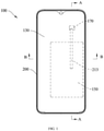
FIG. 1 is a schematic diagram illustrating a front projection of an electronic device provided by the embodiments of the disclosure. -
FIG. 2 is an exploded view of the electronic device shown inFIG. 1 . -
FIG. 3 is a schematic cross-sectional view of the electronic device shown inFIG. 1 taken along line A-A. -
FIG. 4 is an enlarged schematic diagram of region IV of the electronic device shown inFIG. 3 . -
FIG. 5 is a schematic cross-sectional view of the electronic device shown inFIG. 1 taken along line B-B. -
FIG. 6 is an enlarged schematic diagram of an implementation of region V of the electronic device shown inFIG. 5 . -
FIG. 7 is an enlarged schematic diagram of another implementation of region V of the electronic device shown inFIG. 5 . -
FIG. 8 is a schematic cross-sectional view of the heat-conducting element of the electronic device shown inFIG. 1 . - The technical solutions in the embodiments of the present disclosure will be clearly and comprehensively described below in conjunction with the drawings in the embodiments of the present disclosure. Obviously, the described embodiments are only a part of the embodiments of the present disclosure, rather than all the embodiments. Based on the embodiments in this disclosure, all other embodiments obtained by those of ordinary skill in the art without any creative work shall fall within the protection scope of this disclosure.
- The technical solutions in the embodiments of the present disclosure will be clearly and comprehensively described below in conjunction with the drawings in the embodiments of the present disclosure.
- In the related electronic devices, the heat dissipation is mainly performed by adding a heat dispersing material with a good thermal conductivity, such as graphite or copper foil, inside the electronic device, so that the heat is transferred, through the heat dispersing material, to the metal part of the casing of the electronic device, and finally is dissipated to the outside of the electronic device, to lower the temperature of the electronic device. However, since different electronic components are located at different locations, heat concentration can be easily caused in the electronic device. In this case, by arranging the heat dispersing material such as the graphite or copper foil, it is insufficient to dissipate the heat concentrated at each location in time. Thus, the electronic device has a poor heat dissipation effect.
- In view of this, the inventor has conducted a lot of researches on the heat dissipation structure of the electronic device. The inventor found that the local overheating of the electronic device can be avoided by means of a heat pipe that guides the heat generated at the heat source to a battery compartment for heat balance and dissipation. In addition, in order not to increase the thickness of the mobile phone, the battery compartment may be perforated locally. However, due to the perforation in the battery compartment, a lower end of the heat pipe is likely to be partially dislocated during the reliability test and the use of the whole device, which may damage the battery and bring safety hazards to the electronic device.
- Accordingly, the inventor continues to study how to prevent the dislocation of the heat pipe and thus protect the battery without changing the thickness of the electronic device, so as to realize the heat balance and heat dissipation of the electronic device, thereby improving the heat dissipation performance of the electronic device. Among them, the inventor has researched how to avoid the dislocation of the heat pipe in the electronic device, how to make the positions of the heat pipe and the battery relatively fixed, how to make the heat dissipation structure dissipate the heat rapidly in the electronic device, and so on. After a large number of comparisons and researches, the inventor further conducted research on how to design a heat dissipation structure that enables heat balance in the electronic device, and thus proposed the technical solutions of the embodiments of the present disclosure.
- Referring to
FIG. 1 andFIG. 2 , the embodiments of the present disclosure provide anelectronic device 100. Theelectronic device 100 may be, but is not limited to, a mobile phone, a tablet computer, a smart watch and other electronic devices. It is illustrated in the embodiments of the disclosure by taking a case where theelectronic device 100 is a mobile phone as an example. - The
electronic device 100 includes ahousing 200, adisplay panel 130, a firstelectronic component 150, and a secondelectronic component 170. Thehousing 200 and thedisplay panel 130 cooperatively define a receiving cavity, and the firstelectronic component 150 and the secondelectronic component 170 are accommodated in the receiving cavity. Thehousing 200 can provide protection for the firstelectronic component 150 and the secondelectronic component 170, to prevent the firstelectronic component 150 and the secondelectronic component 170 from being dislocated or damaged under the impact of an external force, thereby prolonging the service life of theelectronic device 100. - In the embodiments of the present disclosure, the
display panel 130 is a screen capable of displaying related interfaces or information of theelectronic device 100 for the user to watch or operate. In the embodiments, the firstelectronic component 150 is a battery, that is, the firstelectronic component 150 is an energy supply component of theelectronic device 100 that provides the power required for the normal operation of theelectronic device 100. The secondelectronic component 170 includes any one or more of a central processing unit, a camera, a fingerprint recognition module, and a sensor. The secondelectronic component 170 is electrically connected with thedisplay panel 130 and the firstelectronic component 150 to enable the related functions of theelectronic device 100. The specific structures of the firstelectronic component 150, the secondelectronic component 170 and thedisplay panel 130 are not detailed here. - It should be noted that the first
electronic component 150 and the secondelectronic component 170 generate heat during operation, and the heat generated by the firstelectronic component 150 and the secondelectronic component 170 accounts for a large proportion of the heat generated by theelectronic device 100, that is, the first and second electronic components are the main heat source of the electronic device. In other words, the heat generated by the firstelectronic component 150 and the secondelectronic component 170 would cause theelectronic device 100 to heat, which affects the usage experience and service life of theelectronic device 100. - Referring to
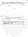
FIG. 3 , thehousing 200 includes amiddle frame 210, a heat-conductingelement 230 and aprotective member 250. Themiddle frame 210 is provided with afirst receiving area 211, and thefirst receiving area 211 is configured to install the firstelectronic component 150. Themiddle frame 210 is further provided with anaccommodating groove 213. Theaccommodating groove 213 penetrates themiddle frame 210 in a thickness direction of the middle frame, and is communicated with thefirst receiving area 211. The heat-conductingelement 230 is accommodated in theaccommodating groove 213. Theprotective member 250 is at least partially accommodated in theaccommodating groove 213, and is located on a side of the heat-conductingelement 230 that faces towards thefirst receiving area 211. - The
protective member 250 is arranged opposite or in contact with the firstelectronic component 150 provided in thefirst receiving area 211. As such, the heat generated by the firstelectronic component 150 is transferred, through theprotective member 250 and the heat-conductingelement 230, to other locations of theelectronic device 100, and then is dissipated to the outside. Accordingly, the heat balance of theelectronic device 100 is achieved, and the local overheating of theelectronic device 100 is avoided, thereby improving the heat dissipation efficiency of theelectronic device 100. In addition, by providing theprotective member 250, it is possible to prevent the firstelectronic component 150 from being damaged by the heat-conductingelement 230 when the heat-conducting element is dislocated (for example, when it is impacted by an external force, or when the structure is loose), thereby improving the reliability of theelectronic device 100. - Specifically, the
middle frame 210 is configured to install or carry the firstelectronic component 150 and the secondelectronic component 170 to limit the positions of the firstelectronic component 150 and the secondelectronic component 170, thereby avoiding malfunction of theelectronic device 100 from being caused by the displacement of the first electronic component150 and the secondelectronic component 170. - In the embodiments, the
middle frame 210 is further provided with asecond receiving area 215. Thesecond receiving area 215 is configured to install the secondelectronic component 170 to limit the position of the secondelectronic component 170. Further, thesecond receiving area 215 and thefirst receiving area 211 are located on a same side of themiddle frame 210, and thesecond receiving area 215 is arranged adjacent to thefirst receiving area 211. Correspondingly, the firstelectronic component 150 and the secondelectronic component 170 are located on the same side of themiddle frame 210. Optionally, the volume of the secondelectronic component 170 is smaller than the volume of the firstelectronic component 150. Therefore, the space occupied by thesecond receiving area 215 in themiddle frame 210 may be smaller than the space occupied by thefirst receiving area 211 in themiddle frame 210. - Referring to
FIG. 4 , in the embodiments of the present disclosure, themiddle frame 210 includes afirst surface 212 and asecond surface 214 that face away from each other. Thefirst receiving area 211 and thesecond receiving area 215 are both provided on thefirst surface 212. Optionally, thefirst receiving area 211 and thesecond receiving area 215 each have a frame-like structure protruding from thefirst surface 212, to limit the positions of the firstelectronic component 150 and the secondelectronic component 170. It is understandable that, when thefirst receiving area 211 and thesecond receiving area 215 are in the frame-like structures, thefirst surface 212 may serve as the bottom wall of thefirst receiving area 211 and thesecond receiving area 215, so that the firstelectronic component 150 received in thefirst receiving area 211 and the secondelectronic component 170 received in thesecond receiving area 215 are further confined. - In some embodiments, the
first receiving area 211 and thesecond receiving area 215 may be located on opposite sides of themiddle frame 210. For example, thefirst receiving area 211 is provided on thefirst surface 212, and thesecond receiving area 215 is provided on thesecond surface 214. - It should be noted that the division of the
first receiving area 211 and thesecond receiving area 215 is just to distinguish the area where the firstelectronic component 150 is received from the area where the secondelectronic component 170 is received in theelectronic device 100, for ease of description, which does not limit the embodiments. - Referring to
FIG. 5 , in the embodiment of the present disclosure, thedisplay panel 130 is disposed on a side of themiddle frame 210 that is away from thefirst receiving area 211, that is, thedisplay panel 130 is substantially opposite to thesecond surface 214. Through this arrangement, thedisplay panel 130 is arranged on one side of themiddle frame 210, and the firstelectronic component 150 and the secondelectronic component 170 are arranged on the opposite side of themiddle frame 210, that is, thedisplay panel 130 and the first and secondelectronic component middle frame 210, so that the internal structure of theelectronic device 100 is reasonable. - Further, referring to
FIG. 6 , themiddle frame 210 further includes aninner wall 217 located between the first and second surfaces, and theaccommodating groove 213 is enclosed by theinner wall 217. Theaccommodating groove 213 penetrates thefirst surface 212 and thesecond surface 214, and is communicated with thefirst receiving area 211 and thesecond receiving area 215. That is, theaccommodating groove 213 penetrates the bottom walls of thefirst receiving area 211 and thesecond receiving area 215. - In the embodiments of the present disclosure, the
accommodating groove 213 is substantially a rectangular groove, and thefirst receiving area 211 and thesecond receiving area 215 are respectively provided at two ends of theaccommodating groove 213. The two ends of theaccommodating groove 213 refer to two relatively short edges of theaccommodating groove 213. Accordingly, two sides of theaccommodating groove 213 refer to two relatively long edges of theaccommodating groove 213. Optionally, when thefirst receiving area 211 and thesecond receiving area 215 are arranged side by side or adjacent to each other, theaccommodating groove 213 may span across thefirst receiving area 211 and thesecond receiving area 215, and be communicated with thefirst receiving area 211 and thesecond receiving area 215. In some embodiments, when thefirst receiving area 211 and thesecond receiving area 215 are located on two opposite sides of themiddle frame 210, the two ends of theaccommodating groove 213 may be communicated with thefirst receiving area 211 and thesecond receiving area 215, respectively. - Referring to
FIG. 6 , theprotective member 250 is disposed in theaccommodating groove 213, and spans across thefirst receiving area 211 and thesecond receiving area 215. In other words, the two opposite ends of theprotective member 250 are respectively located at thefirst receiving area 211 and thesecond receiving area 215, to cover an opening formed by theaccommodating groove 213 in thefirst receiving area 211 and an opening formed by theaccommodating groove 213 in thesecond receiving area 215. - In the embodiments, the
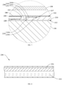
protective member 250 can cover the opening formed by theaccommodating groove 213 in thefirst receiving area 211. For example, theprotective member 250 can cover the side of theaccommodating groove 213 that is communicated with thefirst receiving area 211. By providing theprotective member 250 to cover the opening formed by theaccommodating groove 213, the heat-conductingelement 230 cannot easily fall off from theaccommodating groove 213, thereby improving the heat dissipation stability of thehousing 200. - The
protective member 250 includes amain body 251 and a bent part 253 connected to themain body 251. In the embodiments, themain body 251 is substantially sheet-shaped, and it substantially covers the side of theaccommodating groove 213 that is communicated with thefirst receiving area 211. The bent part 253 is connected with themain body 251 and is bent relative to the main body 241, and the bent part 253 is superposed on theinner wall 217. Themain body 251 is configured to separate the heat-conductingelement 230 from the firstelectronic component 150, to avoid the heat-conductingelement 230 from being in direct contact with the firstelectronic component 150, which would otherwise cause damage to the firstelectronic component 150 when the heat-conductingelement 230 is dislocated. - Optionally, a surface of the
main body 251 away from the heat-conducting element is flush with thefirst surface 212, and is arranged opposite or in direct contact with the firstelectronic component 150. In other words, the side of themain body 251 away from theaccommodating groove 213 is flush with thesecond surface 212. It should be noted that, when themain body 251 is flush with thefirst surface 212, the functions of theprotective member 250 and the heat-conductingelement 230 can be realized without changing the thickness of themiddle frame 210, thereby keeping theelectronic device 100 light and thin. - In the embodiments of the present disclosure, the
protective member 250 bridges thefirst receiving area 211 and thesecond receiving area 215, and is arranged opposite each of the firstelectronic component 150 and the secondelectronic component 170. Therefore, theprotective member 250 also separates the secondelectronic component 170 from the heat-conductingelement 230 to prevent the heat-conductingelement 230 from causing damage to the firstelectronic component 150 and the secondelectronic component 170. - Optionally, the bent part 253 is connected to an edge of the
main body 251, and has a one-time bent structure that is bent once relative to the edge of the main body 251 (as shown inFIG. 6 ). In this case, the bent part 253 extends in a direction facing away from thefirst surface 212. The bent part 253 is substantially perpendicular to themain body 251, and is arranged opposite theinner wall 217, so that a receiving space is defined jointly by the bent part 253 and the main body 521. The accommodating space can be configured to accommodate the heat-conductingelement 230, so as to facilitate the installation and positioning of the heat-conductingelement 230. - Optionally, referring to
FIG. 7 , the bent part 253 is connected to an edge of themain body 251, and has a double-bent structure that is bent twice relative to the edge of themain body 251. In this case, thehousing 200 may further include a mountingpart 219 configured to bear the double-bent structure, so as to limit the position of the double-bent structure. Specifically, the mountingpart 219 is connected to theinner wall 217. The mountingpart 219 is a protrusion protruding from theinner wall 217 toward theaccommodating groove 213. - In the embodiments of the present disclosure, the bent part 253 may be superposed on the mounting
part 219. Specifically, the mountingpart 219 includes anend surface 2191 that is away from theinner wall 217, and aside surface 2193 connected between theend surface 2191 and theinner wall 217. Theside surface 2193 faces away from thefirst surface 212. The mountingpart 219 also includes a connecting surface (not shown in the figure) away from theside surface 2193 and flush with thefirst surface 212. Further, the side surface of the mountingpart 219 that is away from thefirst receiving area 211 is recessed relative to thesecond surface 214 of themiddle frame 210, to form a stepped structure. That is, a distance between the connecting surface and theside surface 2193 is smaller than a distance between thefirst surface 212 and thesecond surface 214. - Further, the bent part 253 includes a first
bent portion 2531 and a secondbent portion 2533. The firstbent portion 2531 is connected between themain body 251 and the secondbent portion 2533. The firstbent portion 2531 is superposed on theend surface 2191, and the secondbent portion 2533 is superposed on theside surface 2193. In the embodiments of the present disclosure, themain body 251 is generally sheet-shaped, and is flush with thefirst surface 212. The firstbent portion 2531 is connected to an edge of themain body 251 and is bent relative to themain body 251, and extends in a direction facing away from the firstelectronic component 150. An included angle between the firstbent portion 2531 and themain body 251 is approximately 90°, so that the firstbent portion 2531 is opposite to theend surface 2191. It can be understood that, the included angle between the firstbent portion 2531 and themain body 251 can be any angle, to limit the heat-conductingelement 230 and improve the protection of the heat-conductingelement 230. - Further, a plane where the second
bent portion 2533 is located is substantially parallel to a plane where themain body 251 is located. For example, the secondbent portion 2533 is connected to an end of the firstbent portion 2531 away from themain body 251 and is bent relative to the firstbent portion 2531, and extends toward theinner wall 217. An included angle between the firstbent portion 2531 and the secondbent portion 2533 is also approximately 90°, so that the secondbent portion 2533 is opposite to and superposed on theside surface 2193. It can be understood that the included angle between the secondbent portion 2533 and the firstbent portion 2531 can be any angle to match the stepped structure formed by the mountingpart 219 and thesecond surface 214, so that the connection between theprotective member 250 and the mountingpart 219 is relatively stable. As such, it is possible to prevent theprotective member 250 from falling off and thus prevent the isolation, provided by theprotective member 250, between the heat-conductingelement 230 and the firstelectronic component 150 from being affected by such falling off. - Optionally, there are two mounting
parts 219 disposed opposite each other in the accommodating groove to further limit the position of theprotective member 250 when the protective member is accommodated in theaccommodating groove 213. Correspondingly, the protective member includes two bent parts 253 respectively connected to opposite sides of themain body 251, and each of the two bent parts is superposed on a respective one of the two mountingparts 219, thereby improving the protection to the heat-conductingelement 230. Further, by limiting the position of theprotective member 250 through the twoend surfaces 2191 of the two mountingparts 219, theprotective member 250 can be prevented from shaking when theprotective member 250 is accommodated in theaccommodating groove 213. - In the embodiments of the present disclosure, the
protective member 250 is made from a metal sheet with a good thermal conductivity, such as a copper sheet or an iron sheet, so as not to affect the heat transferring effect of the heat-conductingelement 230 while playing a role in protection. Themain body 251, the firstbent portion 2531, and the secondbent portion 2533 may be integrally formed, for example by die-casting, stamping, and other processes. - Referring to
FIG. 7 , the heat-conductingelement 230 is accommodated in theaccommodating groove 213, and is disposed on a side of theprotective member 250 that is away from the firstelectronic component 150. The heat-conductingelement 230 is opposite to themain body 251, and the bent part 253 limits the position of the heat-conductingelement 230. In the present embodiment, opposite ends of the heat-conductingelement 230 are located at positions corresponding to thefirst receiving area 211 and thesecond receiving area 215, respectively, so that the heat-conductingelement 230 can balance the heat of thefirst receiving area 211 and the heat of thesecond receiving area 215. Optionally, when the protective member includes two bent parts 253, the two bent parts 253 are respectively connected to opposite sides of themain body 251 to form two opposite ends of theprotective member 250. The two opposite ends of theprotective member 250 correspond to the opposite ends of the heat-conductingelement 230, respectively, to limit the position of the heat-conductingelement 230, thereby preventing the heat-conductingelement 230 from shaking side to side. It should be noted that, since theprotective member 250 is fixed in theaccommodating groove 213, it will not be displaced due to shaking. Accordingly, even if the heat-conductingelement 230 is dislocated, it will not damage the firstelectronic component 150, which improves the reliability of theelectronic device 100. - Referring to
FIG. 8 , in the embodiments of the present disclosure, the heat-conductingelement 230 is tubular, and the heat-conductingelement 230 is provided with an inner cavity. The heat-conductingelement 230 includes acapillary layer 231 and a workingmedium 233. Thecapillary layer 231 and the workingmedium 233 are both arranged in the inner cavity. The workingmedium 233 is a medium capable of generating gas-liquid phase changes in a sealed space, such as water, alcohols, and chlorofluorocarbons (CFC) substitutes. Since the workingmedium 233 needs to absorb a lot of heat when it is transformed from the liquid phase to the gas phase, and the workingmedium 233 in the gas phase transfers heat from one location to another location during the process of spreading toward the surroundings, the heat conduction is realized in theelectronic device 100. Thus, the heat balance and heat dissipation of theelectronic device 100 are realized. The heat balance of theelectronic device 100 means that the local heat in theelectronic device 100 is transferred and dispersed to prevent the heat from being concentrated in a local portion of theelectronic device 100. - Further, the
capillary layer 231 has tiny concave-convex structures, such as pores, grooves and protrusions, to increase the surface area of thecapillary layer 231 and facilitate the adhesion of the workingmedium 233 in the gas phase to thecapillary layer 231, thereby improving the speed at which the workingmedium 233 in the gas phase is condensed into the workingmedium 233 in the liquid phase, and thus improving the heat dissipation performance of theelectronic device 100. The specific structure of thecapillary layer 231 may include one of a porous structure, a fibrous structure, a groove structure, and a net structure, or a combination thereof. Optionally, thecapillary layer 231 may be an independent element, for example, thecapillary layer 231 is a metal weaved mesh which is connected to the inner surface of the heat-conductingelement 230 by means of sintering or the like. Also optionally, thecapillary layer 231 may be a tiny structure formed on the inner surface of the heat-conductingelement 230 by etching or the like. - Specifically, the working process of the heat-conducting
element 230 is explained by taking a case where an end of the heat-conductingelement 230 close to the secondelectronic component 170 is an evaporation end, and an end thereof close to the firstelectronic component 150 is a condensation end, as an example. When the evaporation end of the heat-conductingelement 230 close to the secondelectronic component 170 is heated, the workingmedium 233 in the liquid phase absorbs the heat and evaporates at the evaporation end, and becomes the workingmedium 233 in the gas phase to move and spread toward the condensation end. When the workingmedium 233 in the gas phase moves to the condensation end, it can radiate the heat and be condensed into the workingmedium 233 in the liquid phase, to dissipate the heat carried by the workingmedium 233 in the gas phase from themiddle frame 210 through thefirst receiving area 211, to realize the heat balance of theelectronic device 100. In addition, when the workingmedium 233 in the gas phase moves and spreads toward the condensation end, it can also be partially condensed into the workingmedium 233 in the liquid phase, and then flow back, by means of thecapillary layer 231, to the evaporation end to repeat the above working procedures, so as to realize the cyclical movement of the workingmedium 233, thereby speeding up the process of transferring the heat from the evaporation end to the condensation end. - It should be noted that, since the volume of the second
electronic component 170 is smaller compared with the firstelectronic component 150, the local overheating of theelectronic device 100 is likely to be caused when the secondelectronic component 170 generates heat. However, the heat-conductingelement 230 can transfer the heat of the secondelectronic component 170 to the location where the firstelectronic component 150 is located, so as to realize the heat balance of theelectronic device 100. With regard to transferring the heat to the firstelectronic component 150 through the heat-conductingelement 230, it actually means that the heat is transferred to the region where thefirst receiving area 211 is located, so as to realize the heat balance of theelectronic device 100, and then, the heat is dissipated to themiddle frame 210 through thefirst receiving area 211. - Referring to
FIG. 6 again, thehousing 200 may further include anadhesive layer 220, and theadhesive layer 220 is sandwiched between theprotective member 250 and the heat-conductingelement 230. Theadhesive layer 220 may be a layer of adhesive such as glue, or a cohesive body such as a double-sided tape. The cohesive force of theadhesive layer 220 stabilizes the connection between theprotective member 250 and the heat-conductingelement 230, thereby avoiding the separation of theprotective member 250 from the heat-conductingelement 230 under an external force. Thus, it is ensured that theprotective member 250 can reliably isolate the heat-conductingelement 230 from the firstelectronic component 150, to prevent the firstelectronic component 150 from being damaged by the heat-conductingelement 230 when the heat-conductingelement 230 is dislocated. - Continuing to refer to
FIG. 6 , thehousing 200 further includes aheat dissipation element 240. Theheat dissipation element 240 is laid on a side of the heat-conductingelement 230 that is away from theprotective member 250, and is connected to themiddle frame 210. In the embodiments of the present disclosure, theheat dissipation element 240 is superposed on thesecond surface 214 and covers the side of the receivinggroove 213 that is away from thefirst receiving area 211. Further, theheat dissipation element 240 includes at least one of a graphite sheet and a thermally conductive gel. Theheat dissipation element 240 is superposed on the surface of the heat-conductingelement 230 and the surface of themiddle frame 210 to dissipate the heat transferred by the heat-conductingelement 230, so as to improve the heat dissipation performance of theelectronic device 100. Optionally, theheat dissipation element 240 is sheet-shaped, and the sheet-shapedheat dissipation element 240 may be laid on thesecond surface 214, the secondbent portion 2533, and the heat-conductingelement 230 in sequence, so that the secondbent portion 2533 and the heat-conductingelement 230 are not easy to fall off from theaccommodating groove 213, to further strengthen the structure of themiddle frame 210. In addition, the sheet-shapedheat dissipation element 240 can increase the heat dissipation area, thereby increasing the heat dissipation rate. In thehousing 200 and theelectronic device 100 provided in the embodiments of the present disclosure, theprotective member 250 is arranged opposite or in contact with the firstelectronic component 150 provided in thefirst receiving area 211, so as to transfer the heat of thefirst receiving area 211 to other locations of theelectronic device 100, or transfer the heat from other locations to thefirst receiving area 211, thereby realizing the heat balance of theelectronic device 100, avoiding the local overheating of theelectronic device 100, and improving the heat dissipation efficiency of theelectronic device 100. In addition, by providing theprotective member 250, the firstelectronic component 150 can be prevented from being damaged by the heat-conductingelement 230 when the heat-conducting element is dislocated (for example, when it is impacted by an external force, or when the structure is loose), thereby improving the reliability of theelectronic device 100. - In some other embodiments, an electronic device is also provided. The electronic device includes the housing mentioned in the above embodiments, a first electronic component, and a second electronic component. The first electronic component is accommodated in the first receiving area. The second electronic component is connected to the middle frame, and is spaced apart from the first electronic component. The protective member includes a first section and a second section connected to the first section. The first section is arranged opposite the first electronic component, and the second section is arranged opposite the second electronic component.
- In some embodiments, the first electronic component may be a battery to supply power required for the normal operation of the electronic device. The second electronic component may include any one or more of a chip, a central processing unit, a camera, a fingerprint recognition module, and a sensor, so as to realize related functions of the electronic device. The chip may be a driver chip, a detection chip, etc., which will not be detailed here.
- As an implementation, the first electronic component and the second electronic component may be arranged on a same side of the middle frame, or may be arranged on opposite sides of the middle frame. Through the first section and the second section of the protective member, the first electronic component and the second electronic component both can be opposite to the protective member, so as to prevent the first electronic component and the second electronic component from being damaged by the heat-conducting element when the heat-conducting element is dislocated, so as to prolong the service life of electronic equipment.
- The "electronic device" used in the embodiments of this disclosure includes, but is not limited to, a device that receives and sends communication signals via a wired line (for example, via Public Switched Telephone Network (PSTN), Digital Subscriber Line (DSL), a digital cable or direct cable connection, and/or via another data connection/network), and/or via a wireless interface (for example, a wireless interface for cellular network, Wireless Local Area Network (WLAN), digital TV network such as Digital Video Broadcasting Handheld (DVB-H) network, satellite network, or Amplitude Modulation-Frequency Modulation (AM-FM) broadcast transmitter, and/or a wireless interface of another communication terminal). The communication terminal configured to communicate via a wireless interface may be referred to as a "wireless communication terminal", a "wireless terminal" and/or an "electronic device". Examples of the electronic device include, but are not limited to, satellites or cellular phones; Personal Communication System (PCS) terminals that can combine cellular radio phones with data processing, faxing and data communication capabilities; Personal digital assistants (PDA) that can incorporate a radio phone, a pager, Internet/intranet accessing, a web browser, a memo pad, calendar and/or a Global Positioning System (GPS) receiver; and conventional laptop and/or handheld receiver or other electronic device including a radio phone transceiver.
- The foregoing are only preferred embodiments of the disclosure, and are not intended to limit the disclosure. For those skilled in the art, the disclosure can have various modifications and variants. Any modification, equivalent replacement, improvement, etc. made within the spirit and principle of this disclosure shall fall into the protection scope of this disclosure.
Claims (20)
- A housing, for an electronic device, the housing comprising:a middle frame, provided with a first receiving area and an accommodating groove, wherein the first receiving area is configured to receive an electronic component of the electronic device, and the accommodating groove penetrates the middle frame and is communicated with the first receiving area;a heat-conducting element, accommodated in the accommodating groove; anda protective member, wherein the protective member is at least partially accommodated in the accommodating groove, and is located on a side of the heat-conducting element that faces towards the first receiving area.
- The housing as claimed in claim 1, wherein the first receiving area is configured to install a battery of the electronic device; the middle frame is further provided with a second receiving area configured to receive a further electronic component of the electronic device, the second receiving area and the first receiving area are located on a same side of the middle frame; and the accommodating groove is configured to span across the first receiving area and the second receiving area and be communicated with the first receiving area and the second receiving area.
- The housing as claimed in claim 2, wherein the protective member is configured to span across the first receiving area and the second receiving area; one end of the protective member is arranged opposite the first receiving area, and an opposite end of the protective member is arranged opposite the second receiving area.
- The housing as claimed in any one of claims 1 to 3, wherein the heat-conducting element is provided with an inner cavity, and the heat-conducting element comprises a capillary layer and a working medium both provided in the inner cavity.
- The housing as claimed in claim 4, wherein the capillary layer has at least one structure selected from a group consisting of a porous structure, a fibrous structure, a groove structure, and a net structure.
- The housing as claimed in any one of claims 1 to 5, wherein the housing further comprises an adhesive layer sandwiched between the protective member and the heat-conducting element.
- The housing as claimed in any one of claims 1 to 6, wherein the middle frame comprises an inner wall, and the accommodating groove is enclosed by the inner wall; the protective member comprises a main body and a bent part, the bent part being connected with the main body and bent relative to the main body, the main body covering a side of the accommodating groove that is communicated with the first receiving area, and the bent part being arranged opposite the inner wall.
- The housing as claimed in claim 7, wherein the housing further comprises a mounting part connected to the inner wall, the bent part being superposed on the mounting part.
- The housing as claimed in claim 8, wherein a side surface of the mounting part that is away from the first receiving area is recessed with respect to a surface of the middle frame, to form a stepped structure, and the protective member is partially superposed on the side surface of the mounting part that is away from the first receiving area.
- The housing as claimed in any one of claims 8 to 9, wherein the mounting part further comprises an end surface away from the inner wall, and the side surface is connected between the end surface and the inner wall; and wherein the bent part comprises a first bent portion and a second bent portion, the first bent portion being connected between the main body and the second bent portion, the first bent portion being superposed on the end surface, and the second bent portion being superposed on the side surface.
- The housing as claimed in any one of claims 8 to 10, wherein a side of the main body facing away from the accommodating groove is flush with a surface of the middle frame.
- The housing as claimed in any one of claims 8 to 11, wherein another bent part is further comprised; the bent part is connected to one side of the main body, and the another bent part is connected to an opposite side of the main body; and wherein another mounting part is further comprised; the mounting part and the another mounting part are arranged opposite each other, and each of the bent part and the another bent part is superposed on a respective one of the mounting part and the another mounting part.
- The housing as claimed in any one of claims 1 to 12, wherein the protective member is made from a metal sheet.
- The housing as claimed in any one of claims 1 to 13, wherein the housing further comprises a heat dissipation element; the heat dissipation element is overlaid on a side of the heat-conducting element that is away from the protective member, and is connected with the middle frame.
- The housing as claimed in claim 14, wherein the heat dissipation element comprises at least one selected from a group consisting of a graphite sheet and a thermally conductive gel, and the heat dissipation element is superposed on the heat-conducting element and a surface of the middle frame.
- An electronic device, comprising:the housing as claimed in any one of claims 1 to 15;a first electronic component, accommodated in the first receiving area and arranged opposite the protective member; anda display panel, arranged on a side of the middle frame that is away from the first receiving area.
- The electronic device as claimed in claim 16, wherein the electronic device further comprises a second electronic component connected to the middle frame, the second electronic component and the first electronic component being located on a same side of the middle frame; both the first electronic component and the second electronic component are arranged opposite the protective member.
- The electronic device as claimed in claim 16 or 17, wherein the first electronic component is a battery, and the second electronic component comprises one or more selected from a group consisting of a central processing unit, a camera, a fingerprint recognition module, and a sensor.
- An electronic device, comprising:the housing as claimed in any one of claims 1 to 15;a first electronic component, arranged in the first receiving area of the middle frame; anda second electronic component, connected to the middle frame and spaced apart from the first electronic component; wherein the protective member comprises a first section and a second section connected to the first section, the first section is arranged opposite the first electronic component, and the second section is arranged opposite the second electronic component.
- The electronic device as claimed in claim 19, wherein the first electronic component is a battery, and the second electronic component comprises one or more selected from a group consisting of a central processing unit, a camera, a fingerprint recognition module, and a sensor.
Applications Claiming Priority (2)
| Application Number | Priority Date | Filing Date | Title |
|---|---|---|---|
| CN201910508109.9A CN110167322B (en) | 2019-06-12 | 2019-06-12 | Housing and electronic equipment |
| PCT/CN2020/088868 WO2020248744A1 (en) | 2019-06-12 | 2020-05-07 | Housing and electronic device |
Publications (2)
| Publication Number | Publication Date |
|---|---|
| EP3965541A1 true EP3965541A1 (en) | 2022-03-09 |
| EP3965541A4 EP3965541A4 (en) | 2022-06-15 |
Family
ID=67628881
Family Applications (1)
| Application Number | Title | Priority Date | Filing Date |
|---|---|---|---|
| EP20822550.8A Withdrawn EP3965541A4 (en) | 2019-06-12 | 2020-05-07 | HOUSING AND ELECTRONIC DEVICE |
Country Status (4)
| Country | Link |
|---|---|
| US (1) | US11641728B2 (en) |
| EP (1) | EP3965541A4 (en) |
| CN (1) | CN110167322B (en) |
| WO (1) | WO2020248744A1 (en) |
Families Citing this family (8)
| Publication number | Priority date | Publication date | Assignee | Title |
|---|---|---|---|---|
| CN110167322B (en) * | 2019-06-12 | 2021-02-02 | Oppo广东移动通信有限公司 | Housing and electronic equipment |
| CN110730600B (en) * | 2019-10-29 | 2021-01-29 | 维沃移动通信有限公司 | Electronic equipment's casing and electronic equipment |
| CN111432598B (en) * | 2020-03-04 | 2022-05-24 | Oppo广东移动通信有限公司 | Housing assembly for electronic equipment and electronic equipment |
| EP4117405B1 (en) * | 2020-03-24 | 2025-12-31 | Huawei Technologies Co., Ltd. | MOBILE END DEVICE AND CENTER FRAME ARRANGEMENT |
| CN113038797B (en) * | 2021-03-12 | 2023-04-07 | 维沃移动通信有限公司 | Electronic device |
| CN113260228B (en) * | 2021-05-14 | 2022-12-06 | 维沃移动通信有限公司 | Electronic device |
| TWM630195U (en) * | 2022-03-04 | 2022-08-01 | 藍天電腦股份有限公司 | Heat dissipation structure |
| CN117432704A (en) * | 2023-11-23 | 2024-01-23 | Oppo广东移动通信有限公司 | Folding devices, folding casings and electronic equipment |
Family Cites Families (10)
| Publication number | Priority date | Publication date | Assignee | Title |
|---|---|---|---|---|
| TWM522552U (en) * | 2013-07-19 | 2016-05-21 | 超眾科技股份有限公司 | Handheld communication apparatus and thin heat sink thereof |
| CN204482215U (en) | 2015-04-15 | 2015-07-15 | 青岛海信移动通信技术股份有限公司 | A kind of mobile phone radiator structure |
| CN106304817B (en) * | 2015-06-04 | 2019-01-18 | 宏碁股份有限公司 | Electronic device |
| CN105578840B (en) * | 2015-07-31 | 2018-06-15 | 宇龙计算机通信科技(深圳)有限公司 | A kind of mobile terminal |
| US20170367219A1 (en) * | 2016-06-16 | 2017-12-21 | Asia Vital Components Co., Ltd. | Vapor chamber structure |
| CN106207038B (en) * | 2016-08-30 | 2020-01-24 | Oppo广东移动通信有限公司 | Battery protector, manufacturing method thereof, and mobile communication terminal |
| CN109219307B (en) * | 2017-06-30 | 2021-08-17 | 深圳富泰宏精密工业有限公司 | Heat radiation structure and electronic device with same |
| CN108646891A (en) * | 2018-06-11 | 2018-10-12 | Oppo广东移动通信有限公司 | A heat dissipation component and an electronic device |
| CN108777255B (en) * | 2018-06-11 | 2020-07-31 | Oppo广东移动通信有限公司 | A kind of heat dissipation component and electronic equipment |
| CN110167322B (en) * | 2019-06-12 | 2021-02-02 | Oppo广东移动通信有限公司 | Housing and electronic equipment |
-
2019
- 2019-06-12 CN CN201910508109.9A patent/CN110167322B/en not_active Expired - Fee Related
-
2020
- 2020-05-07 EP EP20822550.8A patent/EP3965541A4/en not_active Withdrawn
- 2020-05-07 WO PCT/CN2020/088868 patent/WO2020248744A1/en not_active Ceased
-
2021
- 2021-11-24 US US17/535,169 patent/US11641728B2/en active Active
Also Published As
| Publication number | Publication date |
|---|---|
| EP3965541A4 (en) | 2022-06-15 |
| US11641728B2 (en) | 2023-05-02 |
| CN110167322B (en) | 2021-02-02 |
| CN110167322A (en) | 2019-08-23 |
| US20220087067A1 (en) | 2022-03-17 |
| WO2020248744A1 (en) | 2020-12-17 |
Similar Documents
| Publication | Publication Date | Title |
|---|---|---|
| US11641728B2 (en) | Housing and electronic device | |
| US8325483B2 (en) | Electronic device including a heat conduction member | |
| AU2016244055B2 (en) | Electronic device including an externally-mounted heat pipe | |
| CN212164015U (en) | Mobile terminal, center subassembly and radiator unit | |
| CN105723821A (en) | Cooling structure for portable electronic device | |
| EP2849545A2 (en) | Portable electronic device and battery pack for the same | |
| WO2021018004A1 (en) | Heat conduction device and terminal device | |
| CN210183778U (en) | Shell and electronic equipment | |
| CN212851549U (en) | Heat sinks and electronic equipment | |
| EP1732230B1 (en) | Portable electronic device | |
| CN219876700U (en) | Middle frame assembly and electronic equipment | |
| CN110267491B (en) | Middle frame assembly and electronic equipment | |
| CN211429879U (en) | Mobile terminal | |
| CN110278688B (en) | Housing components and electronic equipment | |
| JP2003142864A (en) | Electronic equipment | |
| JP7541570B2 (en) | Mobile devices | |
| CN212413240U (en) | Key Assemblies and Electronics | |
| CN111432615B (en) | Heat radiation structure and electronic equipment | |
| JP2010072904A (en) | Electronic equipment and heat transport member | |
| WO2021190552A1 (en) | Mobile terminal and middle frame assembly | |
| CN113453479B (en) | Mobile terminals and mid-frame components | |
| CN210130059U (en) | Heat sinks and electronic equipment | |
| CN110149784A (en) | Heat dissipation assembly and electronic equipment | |
| CN101473710B (en) | Electronic device | |
| CN210381726U (en) | Housing components and electronic equipment |
Legal Events
| Date | Code | Title | Description |
|---|---|---|---|
| STAA | Information on the status of an ep patent application or granted ep patent |
Free format text: STATUS: THE INTERNATIONAL PUBLICATION HAS BEEN MADE |
|
| PUAI | Public reference made under article 153(3) epc to a published international application that has entered the european phase |
Free format text: ORIGINAL CODE: 0009012 |
|
| STAA | Information on the status of an ep patent application or granted ep patent |
Free format text: STATUS: REQUEST FOR EXAMINATION WAS MADE |
|
| 17P | Request for examination filed |
Effective date: 20211202 |
|
| AK | Designated contracting states |
Kind code of ref document: A1 Designated state(s): AL AT BE BG CH CY CZ DE DK EE ES FI FR GB GR HR HU IE IS IT LI LT LU LV MC MK MT NL NO PL PT RO RS SE SI SK SM TR |
|
| A4 | Supplementary search report drawn up and despatched |
Effective date: 20220517 |
|
| RIC1 | Information provided on ipc code assigned before grant |
Ipc: H05K 7/20 20060101AFI20220511BHEP |
|
| DAV | Request for validation of the european patent (deleted) | ||
| DAX | Request for extension of the european patent (deleted) | ||
| GRAP | Despatch of communication of intention to grant a patent |
Free format text: ORIGINAL CODE: EPIDOSNIGR1 |
|
| STAA | Information on the status of an ep patent application or granted ep patent |
Free format text: STATUS: GRANT OF PATENT IS INTENDED |
|
| INTG | Intention to grant announced |
Effective date: 20240307 |
|
| STAA | Information on the status of an ep patent application or granted ep patent |
Free format text: STATUS: THE APPLICATION HAS BEEN WITHDRAWN |
|
| 18W | Application withdrawn |
Effective date: 20240409 |