EP3961918A1 - Kristalloszillator und phasenrauschenreduzierungsverfahren dafür - Google Patents
Kristalloszillator und phasenrauschenreduzierungsverfahren dafür Download PDFInfo
- Publication number
- EP3961918A1 EP3961918A1 EP21173900.8A EP21173900A EP3961918A1 EP 3961918 A1 EP3961918 A1 EP 3961918A1 EP 21173900 A EP21173900 A EP 21173900A EP 3961918 A1 EP3961918 A1 EP 3961918A1
- Authority
- EP
- European Patent Office
- Prior art keywords
- crystal oscillator
- level
- voltage level
- circuit
- sinusoidal wave
- Prior art date
- Legal status (The legal status is an assumption and is not a legal conclusion. Google has not performed a legal analysis and makes no representation as to the accuracy of the status listed.)
- Granted
Links
Images




Classifications
-
- H—ELECTRICITY
- H03—ELECTRONIC CIRCUITRY
- H03B—GENERATION OF OSCILLATIONS, DIRECTLY OR BY FREQUENCY-CHANGING, BY CIRCUITS EMPLOYING ACTIVE ELEMENTS WHICH OPERATE IN A NON-SWITCHING MANNER; GENERATION OF NOISE BY SUCH CIRCUITS
- H03B5/00—Generation of oscillations using amplifier with regenerative feedback from output to input
- H03B5/30—Generation of oscillations using amplifier with regenerative feedback from output to input with frequency-determining element being electromechanical resonator
- H03B5/32—Generation of oscillations using amplifier with regenerative feedback from output to input with frequency-determining element being electromechanical resonator being a piezoelectric resonator
- H03B5/36—Generation of oscillations using amplifier with regenerative feedback from output to input with frequency-determining element being electromechanical resonator being a piezoelectric resonator active element in amplifier being semiconductor device
- H03B5/362—Generation of oscillations using amplifier with regenerative feedback from output to input with frequency-determining element being electromechanical resonator being a piezoelectric resonator active element in amplifier being semiconductor device the amplifier being a single transistor
-
- H—ELECTRICITY
- H03—ELECTRONIC CIRCUITRY
- H03B—GENERATION OF OSCILLATIONS, DIRECTLY OR BY FREQUENCY-CHANGING, BY CIRCUITS EMPLOYING ACTIVE ELEMENTS WHICH OPERATE IN A NON-SWITCHING MANNER; GENERATION OF NOISE BY SUCH CIRCUITS
- H03B5/00—Generation of oscillations using amplifier with regenerative feedback from output to input
- H03B5/30—Generation of oscillations using amplifier with regenerative feedback from output to input with frequency-determining element being electromechanical resonator
- H03B5/32—Generation of oscillations using amplifier with regenerative feedback from output to input with frequency-determining element being electromechanical resonator being a piezoelectric resonator
- H03B5/36—Generation of oscillations using amplifier with regenerative feedback from output to input with frequency-determining element being electromechanical resonator being a piezoelectric resonator active element in amplifier being semiconductor device
-
- H—ELECTRICITY
- H03—ELECTRONIC CIRCUITRY
- H03B—GENERATION OF OSCILLATIONS, DIRECTLY OR BY FREQUENCY-CHANGING, BY CIRCUITS EMPLOYING ACTIVE ELEMENTS WHICH OPERATE IN A NON-SWITCHING MANNER; GENERATION OF NOISE BY SUCH CIRCUITS
- H03B5/00—Generation of oscillations using amplifier with regenerative feedback from output to input
- H03B5/30—Generation of oscillations using amplifier with regenerative feedback from output to input with frequency-determining element being electromechanical resonator
- H03B5/32—Generation of oscillations using amplifier with regenerative feedback from output to input with frequency-determining element being electromechanical resonator being a piezoelectric resonator
- H03B5/36—Generation of oscillations using amplifier with regenerative feedback from output to input with frequency-determining element being electromechanical resonator being a piezoelectric resonator active element in amplifier being semiconductor device
- H03B5/364—Generation of oscillations using amplifier with regenerative feedback from output to input with frequency-determining element being electromechanical resonator being a piezoelectric resonator active element in amplifier being semiconductor device the amplifier comprising field effect transistors
-
- H—ELECTRICITY
- H03—ELECTRONIC CIRCUITRY
- H03B—GENERATION OF OSCILLATIONS, DIRECTLY OR BY FREQUENCY-CHANGING, BY CIRCUITS EMPLOYING ACTIVE ELEMENTS WHICH OPERATE IN A NON-SWITCHING MANNER; GENERATION OF NOISE BY SUCH CIRCUITS
- H03B2200/00—Indexing scheme relating to details of oscillators covered by H03B
- H03B2200/006—Functional aspects of oscillators
- H03B2200/0088—Reduction of noise
- H03B2200/009—Reduction of phase noise
Definitions
- the present invention is related to crystal oscillators, and more particularly, to a crystal oscillator and a phase noise reduction method thereof.
- a reference clock For an electronic system such as a phase-locked loop, a reference clock is required. More particularly, phase noise of the reference clock severely impact overall performance of the electronic system, and phase noise related performance is therefore demanding.
- the reference clock can be generated by a crystal oscillator such as a Pierce oscillator or a Colpitts oscillator.
- Proposed methods and related architecture in a related art greatly increase additional circuits to improve overall performance of the crystal oscillator (e.g. reduce phase noise thereof).
- phase noise of the crystal oscillator more particularly, to reduce the phase noise of the reference clock
- an objective of the present invention is to provide a crystal oscillator and a phase noise reduction method thereof, to improve phase noise related performance of an electronic system, and more particularly, to reduce phase noise of a reference clock output from a crystal oscillator of the electronic system.
- the crystal oscillator may comprise a crystal oscillator core circuit, a first bias circuit and a phase noise reduction circuit, where the first bias circuit is coupled to an output terminal of the crystal oscillator core circuit, and the phase noise reduction circuit is coupled to the output terminal of the crystal oscillator core circuit.
- the crystal oscillator core circuit is configured to generate a sinusoidal wave.
- the first bias circuit configured to provide a first voltage level to be a bias voltage of the sinusoidal wave.
- the phase noise reduction circuit is configured to reset the bias voltage of the sinusoidal wave in response to a voltage level of the sinusoidal wave exceeding a specific voltage range.
- FIG. 1 is a diagram illustrating a crystal oscillator 10 according to an embodiment of the present invention.
- the crystal oscillator 10 may comprise a crystal oscillator core circuit 120, a bias circuit such as a direct current (DC) bias circuit 140, a bias resistor Rbias and a pulse wave buffer such as a square wave buffer 160 (which is labeled "NBUF” for brevity).
- the crystal oscillator core circuit 120 may be a Colpitts oscillator as shown in FIG. 1 , which comprises a crystal tank XTAL (which may be referred to as "crystal oscillator (XO)”), capacitors C1 and C2, a transistor and a current source, but the present invention is not limited thereto.
- the crystal oscillator core circuit 120 may be replaced with a Pierce oscillator in some embodiments.
- the DC bias circuit 140 is coupled to an output terminal of the crystal oscillator 120 through the bias resistor Rbias
- the square wave buffer 160 is coupled to the output terminal of the crystal oscillator 120.
- the output terminal of the crystal oscillator and an input terminal of the square wave buffer 160 are coupled to a node of the crystal oscillator 10
- the DC bias circuit 140 is coupled to this node through the bias resistor Rbias, where an input impedance of this node may be indicated by Zin, and Zin is roughly determined by the bias resistor Rbias.
- the crystal oscillator core circuit 120 is designed to have a high quality factor (e.g. greater than or equal to 100000), and is configured to generate a sinusoidal wave.
- the DC bias circuit 140 may comprise one or more transistors as shown in FIG. 1 , and is configured to provide a bias voltage of the sinusoidal wave, such as a DC bias voltage VB.
- the sinusoidal wave is carried on the level of the DC bias voltage VB (more particularly, the sinusoidal wave may regularly vary up and down based on the level of the DC bias voltage VB).
- the pulse wave buffer such as the square wave buffer 160 may generate a pulse wave such as a square wave on an output terminal OUT of the square wave buffer 160 according to the sinusoidal wave.
- the square wave buffer 160 may comprise an inverter or a chain of inverters, wherein when the level of the sinusoidal wave is greater than a threshold (e.g. an input voltage level threshold) of the square wave buffer 160, the square wave may have a first state (e.g. a first logic value such as "1"), and when the level of the sinusoidal wave is less than the threshold of the square wave buffer 160, the square wave may have a second state (e.g. a second logic value such as "0").
- the pulse wave generated by the pulse wave buffer may be a rectangular wave having a duty cycle equal to 50%, such as the square wave.
- the pulse wave generated by the pulse wave buffer may be a rectangular wave having a duty cycle that is not 50%. The following descriptions takes the square wave as an example for illustrative purposes only, and is not meant to be a limitation of the present invention.
- the bias resistor Rbias may contribute a majority of phase noise of the square wave.
- the bias resistor Rbias may contribute noise which has a positive correlation with the resistance of the bias resistor Rbias.
- the higher the resistance of the bias resistor Rbias the higher the noise is generated.
- signal power of the sinusoidal wave has a negative correlation with the resistance of the bias resistor Rbias.
- the higher the resistance of the bias resistor Rbias the higher the signal power of the sinusoidal wave (i.e. the lower the resistance of the bias resistor Rbias, the more the loss of the sinusoidal wave is caused).
- the present invention aims at breaking this trade-off.
- the thermal noise from the bias resistor Rbias will not greatly impact a signal-to-noise ratio (SNR) of the sinusoidal wave on the output terminal of the crystal oscillator core circuit 120.
- the crystal oscillator core circuit 120 can filter out most of the noise caused by the bias resistor Rbias at a certain frequency offset such as 100 kilo Hertz (kHz) relative to the oscillation frequency of the sinusoidal wave.
- the phase noise of the sinusoidal wave can be small, such as -185 decibels relative to the carrier in one Hertz bandwidth (dBc/Hz).
- the phase noise on the output terminal OUT of the square wave buffer may be high (e.g. -165dBc/Hz), however.
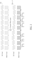
- the sinusoidal wave may be carried on a constant level of VB as illustrated by the waveform labeled "XO Out1" (e.g. a 40 Mega Hertz (MHz) sinusoidal wave may regularly vary up and down based on the constant level of VB), and the pulse width of the square wave may be constant, as illustrated by the waveform labeled "NBUF Out1".
- XO Out1 e.g. a 40 Mega Hertz (MHz) sinusoidal wave may regularly vary up and down based on the constant level of VB
- the pulse width of the square wave may be constant, as illustrated by the waveform labeled "NBUF Out1”.
- the bias resistor Rbias contributes noise (e.g.
- the sinusoidal wave may be carried on a varying level VB+ ⁇ V as illustrated by the waveform labeled "XO Out2" (e.g. a 40 MHz sinusoidal wave may vary up and down based on a time-varying level of a 100 kHz bias noise). Thanks to the characteristics brought from the high quality factor of the crystal oscillator core circuit 120, phase noise of the sinusoidal wave is not significantly increased when the noise of the bias resistor Rbias is considered. For the square wave, the timing of state transition (e.g.
- FIG. 3 is a diagram illustrating a crystal oscillator 30 according to an embodiment of the present invention.
- the crystal oscillator 30 may further comprise a phase noise reduction circuit 180.
- the phase noise reduction circuit 180 is coupled to the output terminal of the crystal oscillator core circuit 120, and may be configured to generate a reset signal comprising at least one reset pulse (e.g. one or more pulses, which may be collectively referred to as the reset pulse) for resetting the bias voltage (e.g. resetting resistor noise on the bias voltage, such as the noise contributed by the bias resistor Rbias) of the sinusoidal wave (e.g.
- the reset signal is generated without calibrating the at least one reset pulse to a zero-crossing point of the sinusoidal wave, where the zero-crossing point of the sinusoidal wave may represents the time point at which the sinusoidal wave varies across the level of the DC bias voltage VB.
- the position of the reset pulse e.g. the timing of the reset pulse relative to the phase of the sinusoidal wave
- the reset pulse can be at the zero-crossing point or peaking of the sinusoidal wave output, and complicated calibration circuits regarding the timing of the reset pulse are not required.
- the phase noise reduction circuit 180 may comprise a reset switch 180SW coupled to the output terminal of the crystal oscillator core circuit 120, and may be controlled by the reset signal.
- the phase noise reduction circuit 180 may further comprise a pulse generator 180G configured to generate the reset signal.
- the reset switch may be turned on in response to the reset pulse, to provide an AC ground path for the resistor noise on the bias voltage to remove the noise on the bias voltage, and thereby reset the bias voltage of the sinusoidal wave to a reset level.
- the reset switch 180SW may be coupled across the bias resistor Rbias, and when the reset switch is turned on, the noise generated by the bias resistor Rbias may be reset, and the varying bias voltage level of the sinusoidal wave can be pulled back to the original voltage level of the DC bias voltage VB, but the present invention is not limited thereto.
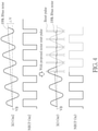
- phase noise reduction circuit 180 solves the problem of the phase noise caused by the bias resistor Rbias, please refer to FIG. 4 .
- the waveforms labeled "XO Out2" and “NBUF Out2” represent the sinusoidal wave on the output terminal of the crystal oscillator core circuit 120 and the square wave on the output terminal of the square wave buffer 160 without using the proposed noise reset pulse (e.g. the phase noise reduction circuit 180 is disabled and the reset switch 180SW is always turned off); and as shown in the lower half-portion of FIG.
- the waveforms labeled "XO Out3" and “NBUF Out3” represent the sinusoidal wave on the output terminal of the crystal oscillator core circuit 120 and the square wave on the output terminal of the square wave buffer 160 with using the proposed noise reset pulse (e.g. the phase noise reduction circuit 180 is enabled and the pulse generator 180G starts to output the reset pulse to periodically turn on the reset switch 180SW).
- the sinusoidal wave may vary up and down based on a time varying level VB+ ⁇ V when the phase noise reduction circuit 180 is disabled, and the pulse width of the square wave is therefore time-varying, which results phase noise.
- the phase noise reduction circuit 180 is enabled and the pulse generator starts to output the reset pulse to the reset switch 180SW (e.g.
- the DC bias voltage level of the sinusoidal wave is therefore reset in response to the reset pulse, and the pulse width of the square wave can be substantially constant, or the varying amount of the bias level of the sinusoidal wave can be reduced (e.g. ⁇ V can be reduced).
- the pulse width of the square wave can be constant or substantially constant, and the phase noise is therefore reduced.
- both of the resistance of the bias resistor Rbias and an input capacitance on the output terminal of the crystal oscillator core circuit 120 can be designed to be quite large, and a large resistance-capacitance (RC) time constant will make the noise of the bias resistor Rbias have insufficient time for greatly change the level of the sinusoidal wave.
- RC resistance-capacitance
- the frequency of the reset signal is preferably to be fast enough to better suppress the noise of the bias resistor Rbias, and thereby maintain the bias voltage level of the sinusoidal wave.
- the frequency of the sinusoidal wave is 40 MHz
- the frequency of the reset signal is 40 MHz
- significant improvements on noise related performance can be observed; and when the frequency of the reset signal is 400 MHz, the noise related performance can be further improved.
- a higher frequency of the reset signal is preferred for obtaining a better noise related performance, but the present invention is not limited thereto.
- the phase noise reduction circuit 180 may further comprise a frequency multiplier configured to generate a signal having a frequency that is N times the frequency of the square wave output from the square wave buffer 160, and accordingly make the frequency of the reset signal is N times the frequency of the square wave (e.g. there may be N reset pulses within one cycle of the sinusoidal wave or the square wave), where N may be a positive integer greater than or equal to two.
- the frequency of the reset signal may be lower than or equal to the frequency of the sinusoidal wave.
- the reset pulse may be periodically generated, and the frequency of the reset pulse may be any suitable positive value.
- the reset pulse is not periodically generated, e.g. the pulse generator 180G may randomly generate the reset pulse or the occurrence of the reset pulse may be controlled by another controller within the crystal oscillator 30.
- the noise generated by the bias resistor Rbias (which is referred to as the Rbias noise for brevity)
- the SNR of the sinusoidal wave there are some factors that may affect the SNR of the sinusoidal wave, such as a turned-on period T ON of the reset pulse (e.g. a pulse width of the reset pulse, which indicates a time length of the reset switch 180SW being turned on), a turned-on resistance R ON of the reset switch 180SW (e.g. a resistance of the reset switch 180SW in a situation where the reset switch 180SW is turned on), and noise corresponding to the turned-on resistance R ON (which is referred to as the R ON noise for brevity).
- a turned-on period T ON of the reset pulse e.g. a pulse width of the reset pulse, which indicates a time length of the reset switch 180SW being turned on
- a turned-on resistance R ON of the reset switch 180SW e.g. a resistance of the reset switch 180SW in a situation where the reset switch 180SW is
- the small ⁇ may be implemented by an exclusive-OR (XOR) logic circuit and a very short delay line, and thereby benefit from small area, low current consumption, and low noise from the delay line.
- XOR exclusive-OR
- the aforementioned very short delay line may comprise one inverter or a chain of inverters, but the present invention is not limited thereto. It should be noted that the delay provided by the aforementioned very short delay line is not limited to a specific value, any delay that is able to reset the bias voltage level of the sinusoidal wave without significantly degrading the SNR, such as 100 picoseconds (ps), 80 ps, etc.
- the first control switch may be conductive in response to the voltage level of the sinusoidal wave being greater than an upper bound level
- the second control switch may be conductive in response to the voltage level of the sinusoidal wave being less than a lower bound level, where the upper bound level and the lower bound level may correspond to the DC voltage levels Vcall and Vcal2, respectively.
- the first control switch may comprise a first diode such as a diode D1
- the second control switch may comprise a second diode such as a diode D2.
- an anode of the diode D1 may be coupled to the output terminal of the crystal oscillator core circuit 120
- a cathode of the diode D1 may be coupled to the DC bias circuit 191.
- an anode of the diode D2 may be coupled to the DC bias circuit 192
- a cathode of the diode D2 may be coupled to the output terminal of the crystal oscillator core circuit 120.
- the diode D1 when a voltage difference between the anode and the cathode of the diode D1 is greater than a threshold voltage Vth1 of the diode D1, the diode D1 can be conductive (e.g. the first control switch may be regarded as being turned on); otherwise, the diode D1 cannot be conductive (e.g. the first control switch may be regarded as being turned off).
- the diode D2 when a voltage difference between the anode and the cathode of the diode D2 is greater than a threshold voltage Vth2 of the diode D2, the diode D2 can be conductive (e.g. the second control switch may be regarded as being turned on); otherwise, the diode D2 cannot be conductive (e.g. the second control switch may be regarded as being turned off).
- any (e.g. each) of the diodes D1 and D2 is not limited to be implemented by a single diode.
- any (e.g. each) of the diodes D1 and D2 may be implemented by a cascode structure of diode units, e.g. N diode units connected in series, to obtain a threshold voltage N ⁇ Vth, depending on the essential voltage swing of the sinusoidal wave, where Vth may represent the threshold voltage by one diode units, and N may represent the number of diode units being connected in series.
- the diode D1 when the voltage level of the sinusoidal wave exceed the upper bound level, the diode D1 may be conductive in response to the voltage difference across the diode D1 exceeding the threshold voltage Vth1, and a maximum level of the sinusoidal wave may therefore be clamped to the upper bound level (e.g. Vcall + N ⁇ Vth) as shown in FIG. 6 ; and when the voltage level of the sinusoidal wave exceed the lower bound level, the diode D2 may be conductive in response to the voltage difference across the diode D1 exceeding the threshold voltage Vth2, and a minimum level of the sinusoidal wave may therefore be clamped to the lower bound level (e.g. Vcal2 - N ⁇ Vth) as shown in FIG. 6 .
- the lower bound level e.g. Vcal2 - N ⁇ Vth
- the diode D1 and/or D2 can be automatically turned on by the voltage swing of the sinusoidal wave, and noise reset regarding the DC bias voltage level of the sinusoidal wave can take effect at the maximum level (e.g. wave peaks) and/or the minimum level (e.g. wave troughs) of the sinusoidal wave as illustrated by a reset current (e.g. a current flowing through the node coupled to the output terminal of the crystal oscillator core circuit 120) shown in FIG. 6 .
- a reset current e.g. a current flowing through the node coupled to the output terminal of the crystal oscillator core circuit 120
- the DC bias circuit 191 may control the DC voltage level Vcall according to a first calibration code such as a three-bit code, where different values (e.g. candidate values such as 111, 110, ..., and 000) of the first calibration code may respectively correspond to different values (e.g. candidate values such as Vcal1(7), Vcal1(6), ..., and Vcal1(0), where Vcal1(7) > Vcal1(6) > ... > Vcal1(0)) of the DC voltage level Vcall.
- the first calibration code is 111
- the DC bias circuit 191 may control the DC voltage level Vcall to be a highest voltage level (e.g.
- the first calibration code may be set to 111 at the beginning, and the DC voltage level Vcall corresponding to this value of the first calibration code is not able to make the condition of turning on the diode D1 occur.
- the first calibration code is therefore stepwise switched to 110, 101, 100, etc., to find at least one value of the first calibration code, which is able to make the condition of turning on the diode D1 occur.
- the DC bias circuit 192 may control the DC voltage level Vcal2 according to a second calibration code such as a three-bit code, where different values (e.g. candidate values such as 111, 110, ..., and 000) of the second calibration code may respectively correspond to different values (e.g.
- the DC bias circuit 192 may control the DC voltage level Vcal2 to be a lowest voltage level (e.g. 0V) within a tuning range of the DC voltage level Vcal2, and when the second calibration code is 000, the DC bias circuit 192 may control the DC voltage level Vcal2 to be a highest voltage level (e.g. 0.9V) within the tuning range of the DC voltage level Vcal2, where the rest values of the second calibration code may be deduced by analogy, e.g.
- ⁇ Vcal2(7), Vcal2(6), Vcal2(5), Vcal2(4), Vcal2(3), Vcal2(2), Vcal2(1), Vcal2(0) ⁇ may be ⁇ 0V, 0.11V, 0.22V, 0.34V, 0.45V, 0.68V, 0.79V, 0.9V ⁇ .
- the second calibration code may be set to 111 at the beginning, and the DC voltage level Vcal2 corresponding to this value of the second calibration code is not able to make the condition of turning on the diode D2 occur.
- the second calibration code is therefore stepwise switched to 110, 101, 100, etc., to find at least one value of the second calibration code, which is able to make the condition of turning on the diode D2 occur.
- the phase noise reduction circuit 190 may further comprise a peak detector 193 coupled to the output terminal of the crystal oscillator core circuit 120, where the peak detector 193 may be configured to detect a swing of the sinusoidal wave to generate a detection result (e.g. detecting a peak value of the sinusoidal wave to obtain information related to the swing), and the DC bias circuits 191 and 192 may respectively control the DC voltage levels Vcall and Vcal2 according to the detection result.
- the peak detector 193 may output a DC voltage according to the swing (or the peak value) of the sinusoidal wave, where this DC voltage may be configured to determine whether the swing of the sinusoidal wave is changed (e.g. reduced), but the present invention is not limited thereto.
- the DC voltage output from the peak detector 193 may be 500mV, and when the swing of the sinusoidal wave is ⁇ 900mV, the DC voltage output from the peak detector 193 may be 450mV It should be noted that those skilled in this art should understand detailed implementation of the peak detector 193 based on the descriptions mentioned above, and related details are omitted here for brevity.
- the ACAL circuit 121 may calibrate the current source by a speed/frequency of the square wave on the output terminal OUT (e.g. modifying the calibration code one time in each cycle of the square wave during the calibration regarding the current source), but the present invention is not limited thereto.
- the DC voltage level Vcall is set to the initial maximum level and the DC voltage level Vcal2 is set to the initial minimum level.
- the ACAL circuit 121 may calibrate the bias current, to make the swing of the sinusoidal wave fall into a range between a tunable maximum level (e.g. an initial level of Vcall + N ⁇ Vth) related to the initial maximum level and a tunable minimum level (e.g. an initial level of Vcal2 - N ⁇ Vth) related to the initial minimum level.
- the calibration regarding the DC voltage levels Vcall and Vcal2 is guaranteed to be started from a condition where the first control switch and the second control switch (e.g. the diode D1 and D2) are unable to be conductive in response to the maximum level and the minimum level of the sinusoidal wave.
- any (e.g. each) of the DC voltage levels Vcall and Vcal2 may be stepwise modified according to the detection result (e.g. the DC voltage output from the peak detector 193), to make the first control switch such as the diode D1 be able to be conductive in response to the maximum level (e.g.
- the DC voltage output from the peak detector 193 is 500mV at the beginning of the calibration regarding the DC voltage levels Vcall and Vcal2.
- the DC voltage level Vcall is decreased by one step (e.g. switching the first calibration code from 111 to 110) and/or the DC voltage level Vcal2 is increased by one step (e.g. switching the second calibration code from 111 to 110)
- the DC voltage level Vcall may be further decreased by another step (e.g.
- switching the first calibration code from 110 to 101 and/or the DC voltage level Vcal2 may be further increased by another step (e.g. switching the second calibration code from 110 to 101); and if the DC voltage output from the peak detector 193 becomes 480mV, which means the swing of the sinusoidal wave is reduced because the noise reset regarding the DC bias voltage level of the sinusoidal wave takes effect, the current values (e.g. the latest values) of the first calibration code and the second calibration code may be the final values of the first calibration code and the second calibration code, respectively, and the calibration regarding the DC voltage levels Vcall and Vcal2 is therefore completed.
- the tuning ranges of the values of voltage levels and calibration codes mentioned above are for illustrative purposes only, and are not meant to be a limitation of the present invention.
- the number of bits of the first calibration code and the second calibration code may vary.
- the turning range of the DC voltage level Vcall may be the same as the tuning range of the DC voltage level Vcal2.
- the tuning range of the DC voltage level Vcall may be different from the tuning range of the DC voltage level Vcal2.
- the calibration of the DC voltage level Vcall and the calibration of the DC voltage level Vcal2 do not have to be performed concurrently.
- the calibration of the DC voltage level Vcal2 may be performed after the calibration of the DC voltage level Vcall is completed.
- the calibration of the DC voltage level Vcall may be performed after the calibration of the DC voltage level Vcal2 is completed.
- some embodiments may perform calibration on one of the DC voltage levels Vcall and Vcal2 only. In practice, it is preferably to calibrate both of the DC voltage levels Vcall and Vcal2 for obtaining a symmetric waveform of the sinusoidal wave.
- the DC voltage levels Vcall and Vcal2 may be calibrated concurrently with aid of the same calibration code (e.g. the first calibration code may be equal to the second calibration code), but the present invention is not limited thereto.
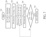
- FIG. 7 illustrates a working flow of the calibration regarding the DC voltage levels Vcall and Vcal2 shown in FIG. 5 according to an embodiment of the present invention.
- a calibration control circuit within the phase noise reduction circuit 190 may utilize multiple control signals for controlling the working flow of the calibration, but the present invention is not limited thereto.
- the working flow shown in FIG. 7 is for illustrative purposes only, and is not meant to be a limitation of the present invention.
- one or more steps may be added, deleted or modified in the working flow shown in FIG. 7 .
- these steps do not have to be executed in the exact order shown in FIG. 7 .
- Step 710 when the crystal oscillator 50 is enabled, the working flow of the calibration starts.
- the calibration control circuit may control the DC bias circuit 191 to set the DC voltage level Vcall to maximum (e.g. the initial maximum level) and control the DC bias circuit 192 to set the DC voltage level Vcal2 to minimum (e.g. the initial minimum level).
- the calibration control circuit may control the DC bias circuit 191 to decrease the DC voltage level Vcall by one step, and control the DC bias circuit 192 to increase the DC voltage level Vcal2 by one step.
- Step 760 the calibration control circuit may determine whether (Vp - Vdet) meets a target (e.g. whether (Vp - Vdet) is greater than a predetermine voltage difference). If the determination result is "Yes”, the working flow proceeds with Step 780; and if the determination result is "No", the working flow proceeds with Step 740.
- Step 770 the calibration control circuit ends the calibration.
- any (e.g. each) of the diodes D1 and D2 does not have to be implemented by typical diodes.
- any device comprising at least one P-N junction may be modified to implement the diodes D1 and D2.
- the diodes D1 may be implemented by a P-type transistor, where a drain and a gate of the P-type transistor may be coupled to each other, to configure this P-type transistor as a diode-connected transistor, which has similar characteristics as typical diodes.
- the diodes D2 may be implemented by an N-type transistor, where a drain and a gate of the N-type transistor may be coupled to each other, to configure this N-type transistor as a diode-connected transistor, which has similar characteristics as typical diodes.
- a drain and a gate of the N-type transistor may be coupled to each other, to configure this N-type transistor as a diode-connected transistor, which has similar characteristics as typical diodes.
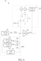
- FIG. 8 is a diagram illustrating a crystal oscillator 80 according to an embodiment of the present invention, where the crystal oscillator 80 may be a modified version or an example of the crystal oscillator 50 shown in FIG. 5 .
- the phase noise reduction circuit 190 may be replaced with a phase noise reduction circuit 190M as shown in FIG. 8 , and more particularly, the diodes D1 and D2 are replaced with a P-type transistor M1 and an N-type transistor M2, respectively.
- FIG. 8 is a diagram illustrating a crystal oscillator 80 according to an embodiment of the present invention, where the crystal oscillator 80 may be a modified version or an example of the crystal oscillator 50 shown in FIG. 5 .
- the phase noise reduction circuit 190 may be replaced with a phase noise reduction circuit 190M as shown in FIG. 8 , and more particularly, the diodes D1 and D2 are replaced with a P-type transistor M1 and an N-type transistor M2, respectively.
- a gate terminal of the P-type transistor M1 is coupled to the DC bias circuit 191 for receiving the DC voltage level Vcall, a drain terminal of the P-type transistor M1 is configured to receive a DC voltage level VB1, and a source terminal of the P-type transistor M1 is coupled to the output terminal of the crystal oscillator core circuit 120.
- a gate terminal of the N-type transistor M2 is coupled to the DC bias circuit 192 for receiving the DC voltage level Vcal2
- a drain terminal of the N-type transistor M2 is configured to receive a DC voltage level VB2
- a source terminal of the N-type transistor M2 is coupled to the output terminal of the crystal oscillator core circuit 120.
- the P-type transistor M1 may be turned on and the DC bias voltage level of the sinusoidal wave may be reset to VB1.
- the minimum level such as the wave troughs of the sinusoidal wave exceeds the lower bound level and thereby makes a difference between the DC voltage level Vcal2 and the voltage level of the sinusoidal wave be greater than a threshold voltage (e.g. making Vcal2 - Vsin >
- a threshold voltage e.g. making Vcal2 - Vsin >
- the DC voltage levels VB 1 and VB2 may be the same. In some embodiments, the DC voltage levels VB 1 and VB2 may be different. In some embodiments, both of the DC voltage levels VB 1 and VB2 may be the same as the DC voltage level of the DC bias voltage VB provided by the DC bias circuit 140. In some embodiments, at least one of DC voltage levels VB1 and VB2 (e.g. one of them or both of them) may be different from the DC voltage level of the DC bias voltage VB provided by the DC bias circuit 140. As long as the DC voltage levels VB1 and VB2 are clean and constant voltage levels (e.g.
- the DC voltage levels VB1 and VB2 are not limited to specific voltage levels.
- the working flow of the calibration regarding the DC voltage levels Vcall and Vcal2 shown in FIG. 5 can also be adopted in the crystal oscillator 80 shown in FIG. 8 .
- similar descriptions related to the calibration regarding the DC voltage levels Vcall and Vcal2 are not repeated here.
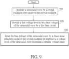
- FIG. 9 illustrates a working flow of a phase noise reduction method of a crystal oscillator (e.g. the crystal oscillator 50 or the crystal oscillator 80) according to an embodiment of the present invention.
- a crystal oscillator e.g. the crystal oscillator 50 or the crystal oscillator 80
- FIG. 9 illustrates a working flow of a phase noise reduction method of a crystal oscillator (e.g. the crystal oscillator 50 or the crystal oscillator 80) according to an embodiment of the present invention.
- the working flow shown in FIG. 9 is for illustrative purposes only, and is not meant to be a limitation of the present invention.
- one or more steps may be added, deleted or modified in the working flow shown in FIG. 9 .
- these steps do not have to be executed in the exact order shown in FIG. 9 .
- the crystal oscillator may provide a first voltage level (e.g. the level of the DC bias voltage VB) to be a bias voltage of the sinusoidal wave by a first bias circuit (e.g. the DC bias circuit 140) of the crystal oscillator.
- a first voltage level e.g. the level of the DC bias voltage VB
- a first bias circuit e.g. the DC bias circuit 140
- the crystal oscillator reset the bias voltage of the sinusoidal wave by a phase noise reduction circuit (e.g. the phase noise reduction circuit 190 shown in FIG. 5 or the phase noise reduction circuit 190M shown in FIG. 8 ) of the crystal oscillator in response to a voltage level of the sinusoidal wave exceeding a specific voltage range.
- a phase noise reduction circuit e.g. the phase noise reduction circuit 190 shown in FIG. 5 or the phase noise reduction circuit 190M shown in FIG. 8
- the noise reset regarding the DC bias voltage level of the sinusoidal wave can take effect at least at the time points of wave peaks or wave troughs of the sinusoidal wave.
- the present invention can improve the phase noise related performance without introducing any side effect or in a way that is less likely to introduce side effects.
- the present invention may also be defined by means of the following numbered clauses.
Landscapes
- Oscillators With Electromechanical Resonators (AREA)
Applications Claiming Priority (2)
| Application Number | Priority Date | Filing Date | Title |
|---|---|---|---|
| US202063070347P | 2020-08-26 | 2020-08-26 | |
| US17/306,960 US11309835B2 (en) | 2020-08-26 | 2021-05-04 | Crystal oscillator and phase noise reduction method thereof |
Publications (2)
| Publication Number | Publication Date |
|---|---|
| EP3961918A1 true EP3961918A1 (de) | 2022-03-02 |
| EP3961918B1 EP3961918B1 (de) | 2024-12-18 |
Family
ID=75936764
Family Applications (1)
| Application Number | Title | Priority Date | Filing Date |
|---|---|---|---|
| EP21173900.8A Active EP3961918B1 (de) | 2020-08-26 | 2021-05-14 | Kristalloszillator und phasenrauschenreduzierungsverfahren dafür |
Country Status (4)
| Country | Link |
|---|---|
| US (2) | US11309835B2 (de) |
| EP (1) | EP3961918B1 (de) |
| CN (1) | CN114123975A (de) |
| TW (1) | TWI746413B (de) |
Families Citing this family (3)
| Publication number | Priority date | Publication date | Assignee | Title |
|---|---|---|---|---|
| US11309835B2 (en) * | 2020-08-26 | 2022-04-19 | Mediatek Inc. | Crystal oscillator and phase noise reduction method thereof |
| CN121461891B (zh) * | 2026-01-05 | 2026-04-03 | 爱科微科技(上海)股份有限公司 | 一种考毕兹晶体振荡器幅度检测装置及其检测、校准方法 |
| CN121441232B (zh) * | 2026-01-05 | 2026-04-03 | 爱科微科技(上海)股份有限公司 | 一种晶体振荡器幅度检测与校准装置及其检测校准方法 |
Citations (4)
| Publication number | Priority date | Publication date | Assignee | Title |
|---|---|---|---|---|
| US20140104009A1 (en) * | 2012-10-12 | 2014-04-17 | Google Inc. | Crystal oscillator with electrostatic discharge (esd) compliant drive level limiter |
| US20160072497A1 (en) * | 2014-09-05 | 2016-03-10 | Marvell World Trade Ltd. | Low Phase Noise Technique for a Crystal Oscillator Circuit |
| US20180109264A1 (en) * | 2016-10-13 | 2018-04-19 | SK Hynix Inc. | Low power crystal oscillation circuits |
| US20190109563A1 (en) * | 2017-10-06 | 2019-04-11 | Realtek Semiconductor Corp. | Crystal oscillator circuit and method thereof |
Family Cites Families (30)
| Publication number | Priority date | Publication date | Assignee | Title |
|---|---|---|---|---|
| US4319204A (en) | 1978-11-14 | 1982-03-09 | Continental Electronics Mfg. Co. | Phase modulated square wave generator |
| US4704587A (en) | 1986-12-04 | 1987-11-03 | Western Digital Corporation | Crystal oscillator circuit for fast reliable start-up |
| US5223801A (en) | 1992-03-30 | 1993-06-29 | Interactive Technologies, Inc. | Crystal oscillator and transmitter operating at the third harmonic of the fifth overtone of a crystal |
| JP3567747B2 (ja) | 1998-07-31 | 2004-09-22 | 富士通株式会社 | 電圧制御発振器及び周波数−電圧変換器 |
| US6683506B2 (en) | 2002-01-18 | 2004-01-27 | The Regents Of The University Of California | CMOS phase locked loop with voltage controlled oscillator having realignment to reference and method for the same |
| US7009460B2 (en) * | 2004-07-21 | 2006-03-07 | Sony Ericsson Mobile Communications Ab | Method and apparatus for reducing the start time of a VCXO |
| FR2882871A1 (fr) | 2005-03-01 | 2006-09-08 | Atmel Corp | Oscillateur commande en tension a multiphase realignee et boucle a phase asservie associee |
| US7339439B2 (en) | 2005-07-18 | 2008-03-04 | Atmel Corporation | Voltage-controlled oscillator with multi-phase realignment of asymmetric stages |
| US7292114B2 (en) * | 2005-08-01 | 2007-11-06 | Marvell World Trade Ltd. | Low-noise high-stability crystal oscillator |
| JP5262901B2 (ja) | 2009-03-26 | 2013-08-14 | セイコーエプソン株式会社 | 発振器 |
| US8143961B2 (en) | 2010-03-30 | 2012-03-27 | Silicon Laboratories Inc. | Technique for detecting crystals |
| US8502565B2 (en) | 2010-07-26 | 2013-08-06 | St-Ericsson Sa | Low phase noise buffer for crystal oscillator |
| JP5570954B2 (ja) | 2010-11-24 | 2014-08-13 | 富士通株式会社 | 発振回路 |
| US9705450B2 (en) | 2011-06-24 | 2017-07-11 | The United States Of America As Represented By The Secretary Of The Navy | Apparatus and methods for time domain measurement of oscillation perturbations |
| CN102332915A (zh) | 2011-07-25 | 2012-01-25 | 复旦大学 | 一种具有宽锁定范围的次谐波注入锁定压控振荡器 |
| US9407201B1 (en) * | 2015-04-17 | 2016-08-02 | Taiwan Semiconductor Manufacturing Company Limited | Crystal oscillator circuit |
| US9837958B2 (en) | 2015-06-08 | 2017-12-05 | Maxlinear, Inc. | Crystal (xtal) oscillator with high interference immunity |
| US10367450B2 (en) | 2015-12-15 | 2019-07-30 | Mediatek Inc. | Oscillator scheme capable of reducing far-out phase noise and closed-in phase noise |
| US9906209B2 (en) | 2016-05-27 | 2018-02-27 | Mediatek Inc. | Biased impedance circuit, impedance adjustment circuit, and associated signal generator |
| CN106656173B (zh) | 2016-12-26 | 2020-01-24 | 上海迦美信芯通讯技术有限公司 | 一种振荡器的频率校准电路及其频率校准方法 |
| US10523155B2 (en) | 2017-08-07 | 2019-12-31 | Microchip Technology Incorporated | Low-voltage crystal oscillator circuit compatible with GPIO |
| CN108123683B (zh) * | 2017-12-08 | 2021-08-10 | 张家港康得新光电材料有限公司 | 一种晶振电路 |
| US10432143B2 (en) | 2017-12-25 | 2019-10-01 | Shenzhen GOODIX Technology Co., Ltd. | Circuit and method for facilitating startup time of crystal oscillator |
| US10680585B2 (en) | 2018-04-09 | 2020-06-09 | Ciena Corporation | Techniques and circuits for time-interleaved injection locked voltage controlled oscillators with jitter accumulation reset |
| US10848101B2 (en) | 2018-11-30 | 2020-11-24 | Arm Limited | Output buffer for single-pin crystal oscillators |
| US10833633B2 (en) | 2018-12-19 | 2020-11-10 | Semiconductor Components Industries, Llc | Circuit and method for controlling a crystal oscillator |
| US11082006B2 (en) | 2019-01-23 | 2021-08-03 | Stmicroelectronics International N.V. | Low power crystal oscillator |
| US10840897B1 (en) | 2019-10-31 | 2020-11-17 | Silicon Laboratories Inc. | Noise canceling technique for a sine to square wave converter |
| US11342884B2 (en) * | 2020-08-26 | 2022-05-24 | Mediatek Inc. | Crystal oscillator and phase noise reduction method thereof |
| US11309835B2 (en) * | 2020-08-26 | 2022-04-19 | Mediatek Inc. | Crystal oscillator and phase noise reduction method thereof |
-
2021
- 2021-05-04 US US17/306,960 patent/US11309835B2/en active Active
- 2021-05-14 EP EP21173900.8A patent/EP3961918B1/de active Active
- 2021-06-03 TW TW110120190A patent/TWI746413B/zh active
- 2021-06-22 CN CN202110689859.8A patent/CN114123975A/zh active Pending
-
2022
- 2022-03-14 US US17/693,454 patent/US11671056B2/en active Active
Patent Citations (4)
| Publication number | Priority date | Publication date | Assignee | Title |
|---|---|---|---|---|
| US20140104009A1 (en) * | 2012-10-12 | 2014-04-17 | Google Inc. | Crystal oscillator with electrostatic discharge (esd) compliant drive level limiter |
| US20160072497A1 (en) * | 2014-09-05 | 2016-03-10 | Marvell World Trade Ltd. | Low Phase Noise Technique for a Crystal Oscillator Circuit |
| US20180109264A1 (en) * | 2016-10-13 | 2018-04-19 | SK Hynix Inc. | Low power crystal oscillation circuits |
| US20190109563A1 (en) * | 2017-10-06 | 2019-04-11 | Realtek Semiconductor Corp. | Crystal oscillator circuit and method thereof |
Also Published As
| Publication number | Publication date |
|---|---|
| US11309835B2 (en) | 2022-04-19 |
| CN114123975A (zh) | 2022-03-01 |
| TWI746413B (zh) | 2021-11-11 |
| US11671056B2 (en) | 2023-06-06 |
| TW202209812A (zh) | 2022-03-01 |
| US20220209714A1 (en) | 2022-06-30 |
| US20220069773A1 (en) | 2022-03-03 |
| EP3961918B1 (de) | 2024-12-18 |
Similar Documents
| Publication | Publication Date | Title |
|---|---|---|
| US11671056B2 (en) | Crystal oscillator and phase noise reduction method thereof | |
| US9099994B2 (en) | Relaxation oscillator | |
| US8525603B2 (en) | Oscillating signal generating device and related method | |
| US8930428B2 (en) | Random number generation circuit | |
| CN112152597B (zh) | 针对单稳态的pvt补偿延迟单元 | |
| EP2654379A1 (de) | Hochstabile dämpfungsvorrichtung | |
| US8384457B2 (en) | Duty cycle correction | |
| US11606063B2 (en) | Crystal oscillator and phase noise reduction method thereof | |
| KR102010434B1 (ko) | 주입 동기 주파수 체배기 및 그의 주파수 체배 방법 | |
| US7830190B2 (en) | Data latch circuit with a phase selector | |
| US20050225351A1 (en) | Method for detecting a power load of a power supply module according to duty cycle detection, and related device | |
| US8433990B2 (en) | Semiconductor test apparatus and test method | |
| CN111106826B (zh) | 时脉产生电路及其时脉调整方法 | |
| US8461883B2 (en) | Frequency generator | |
| CN111308310B (zh) | 一种氮化镓器件的动态Rds(on)参数测试机 | |
| EP3799298B1 (de) | Verfahren zum starten eines kristalloszillators mit hilfe einer externen taktinjektion und zugehöriger kristalloszillator | |
| EP2501041A1 (de) | Frequenzbestimmungsvorrichtung, spannungskomparatorschaltung und frequenzmessvorrichtung | |
| EP4387103A1 (de) | Phasenregelkreis | |
| US12316277B2 (en) | Low power mode control module and method for crystal oscillator, and circuit using the same | |
| TW569540B (en) | Ring oscillator with faster response by current-guiding circuit | |
| KR102875447B1 (ko) | 주파수 발생 회로 | |
| JP2008304255A (ja) | 半導体装置 | |
| WO2007078693A1 (en) | Method and apparatus for 0/180 degree phase detector | |
| CN115684985A (zh) | 用于开关电源的检测电路、方法、芯片和电子设备 | |
| Pristavu et al. | Fully-integrated oscillator in CMOS technology |
Legal Events
| Date | Code | Title | Description |
|---|---|---|---|
| PUAI | Public reference made under article 153(3) epc to a published international application that has entered the european phase |
Free format text: ORIGINAL CODE: 0009012 |
|
| STAA | Information on the status of an ep patent application or granted ep patent |
Free format text: STATUS: THE APPLICATION HAS BEEN PUBLISHED |
|
| AK | Designated contracting states |
Kind code of ref document: A1 Designated state(s): AL AT BE BG CH CY CZ DE DK EE ES FI FR GB GR HR HU IE IS IT LI LT LU LV MC MK MT NL NO PL PT RO RS SE SI SK SM TR |
|
| STAA | Information on the status of an ep patent application or granted ep patent |
Free format text: STATUS: REQUEST FOR EXAMINATION WAS MADE |
|
| 17P | Request for examination filed |
Effective date: 20220818 |
|
| RBV | Designated contracting states (corrected) |
Designated state(s): AL AT BE BG CH CY CZ DE DK EE ES FI FR GB GR HR HU IE IS IT LI LT LU LV MC MK MT NL NO PL PT RO RS SE SI SK SM TR |
|
| P01 | Opt-out of the competence of the unified patent court (upc) registered |
Effective date: 20230607 |
|
| RIC1 | Information provided on ipc code assigned before grant |
Ipc: H03B 5/36 20060101AFI20240514BHEP |
|
| GRAP | Despatch of communication of intention to grant a patent |
Free format text: ORIGINAL CODE: EPIDOSNIGR1 |
|
| STAA | Information on the status of an ep patent application or granted ep patent |
Free format text: STATUS: GRANT OF PATENT IS INTENDED |
|
| INTG | Intention to grant announced |
Effective date: 20240712 |
|
| GRAS | Grant fee paid |
Free format text: ORIGINAL CODE: EPIDOSNIGR3 |
|
| GRAA | (expected) grant |
Free format text: ORIGINAL CODE: 0009210 |
|
| STAA | Information on the status of an ep patent application or granted ep patent |
Free format text: STATUS: THE PATENT HAS BEEN GRANTED |
|
| AK | Designated contracting states |
Kind code of ref document: B1 Designated state(s): AL AT BE BG CH CY CZ DE DK EE ES FI FR GB GR HR HU IE IS IT LI LT LU LV MC MK MT NL NO PL PT RO RS SE SI SK SM TR |
|
| REG | Reference to a national code |
Ref country code: CH Ref legal event code: EP |
|
| REG | Reference to a national code |
Ref country code: DE Ref legal event code: R096 Ref document number: 602021023437 Country of ref document: DE |
|
| REG | Reference to a national code |
Ref country code: IE Ref legal event code: FG4D |
|
| REG | Reference to a national code |
Ref country code: LT Ref legal event code: MG9D |
|
| PG25 | Lapsed in a contracting state [announced via postgrant information from national office to epo] |
Ref country code: HR Free format text: LAPSE BECAUSE OF FAILURE TO SUBMIT A TRANSLATION OF THE DESCRIPTION OR TO PAY THE FEE WITHIN THE PRESCRIBED TIME-LIMIT Effective date: 20241218 |
|
| PG25 | Lapsed in a contracting state [announced via postgrant information from national office to epo] |
Ref country code: FI Free format text: LAPSE BECAUSE OF FAILURE TO SUBMIT A TRANSLATION OF THE DESCRIPTION OR TO PAY THE FEE WITHIN THE PRESCRIBED TIME-LIMIT Effective date: 20241218 |
|
| PG25 | Lapsed in a contracting state [announced via postgrant information from national office to epo] |
Ref country code: BG Free format text: LAPSE BECAUSE OF FAILURE TO SUBMIT A TRANSLATION OF THE DESCRIPTION OR TO PAY THE FEE WITHIN THE PRESCRIBED TIME-LIMIT Effective date: 20241218 |
|
| PG25 | Lapsed in a contracting state [announced via postgrant information from national office to epo] |
Ref country code: NO Free format text: LAPSE BECAUSE OF FAILURE TO SUBMIT A TRANSLATION OF THE DESCRIPTION OR TO PAY THE FEE WITHIN THE PRESCRIBED TIME-LIMIT Effective date: 20250318 |
|
| REG | Reference to a national code |
Ref country code: NL Ref legal event code: MP Effective date: 20241218 |
|
| PG25 | Lapsed in a contracting state [announced via postgrant information from national office to epo] |
Ref country code: LV Free format text: LAPSE BECAUSE OF FAILURE TO SUBMIT A TRANSLATION OF THE DESCRIPTION OR TO PAY THE FEE WITHIN THE PRESCRIBED TIME-LIMIT Effective date: 20241218 Ref country code: GR Free format text: LAPSE BECAUSE OF FAILURE TO SUBMIT A TRANSLATION OF THE DESCRIPTION OR TO PAY THE FEE WITHIN THE PRESCRIBED TIME-LIMIT Effective date: 20250319 |
|
| PG25 | Lapsed in a contracting state [announced via postgrant information from national office to epo] |
Ref country code: RS Free format text: LAPSE BECAUSE OF FAILURE TO SUBMIT A TRANSLATION OF THE DESCRIPTION OR TO PAY THE FEE WITHIN THE PRESCRIBED TIME-LIMIT Effective date: 20250318 |
|
| PG25 | Lapsed in a contracting state [announced via postgrant information from national office to epo] |
Ref country code: NL Free format text: LAPSE BECAUSE OF FAILURE TO SUBMIT A TRANSLATION OF THE DESCRIPTION OR TO PAY THE FEE WITHIN THE PRESCRIBED TIME-LIMIT Effective date: 20241218 |
|
| REG | Reference to a national code |
Ref country code: AT Ref legal event code: MK05 Ref document number: 1753061 Country of ref document: AT Kind code of ref document: T Effective date: 20241218 |
|
| PG25 | Lapsed in a contracting state [announced via postgrant information from national office to epo] |
Ref country code: SM Free format text: LAPSE BECAUSE OF FAILURE TO SUBMIT A TRANSLATION OF THE DESCRIPTION OR TO PAY THE FEE WITHIN THE PRESCRIBED TIME-LIMIT Effective date: 20241218 |
|
| PG25 | Lapsed in a contracting state [announced via postgrant information from national office to epo] |
Ref country code: PL Free format text: LAPSE BECAUSE OF FAILURE TO SUBMIT A TRANSLATION OF THE DESCRIPTION OR TO PAY THE FEE WITHIN THE PRESCRIBED TIME-LIMIT Effective date: 20241218 |
|
| PGFP | Annual fee paid to national office [announced via postgrant information from national office to epo] |
Ref country code: DE Payment date: 20250325 Year of fee payment: 5 |
|
| PG25 | Lapsed in a contracting state [announced via postgrant information from national office to epo] |
Ref country code: ES Free format text: LAPSE BECAUSE OF FAILURE TO SUBMIT A TRANSLATION OF THE DESCRIPTION OR TO PAY THE FEE WITHIN THE PRESCRIBED TIME-LIMIT Effective date: 20241218 |
|
| PG25 | Lapsed in a contracting state [announced via postgrant information from national office to epo] |
Ref country code: IS Free format text: LAPSE BECAUSE OF FAILURE TO SUBMIT A TRANSLATION OF THE DESCRIPTION OR TO PAY THE FEE WITHIN THE PRESCRIBED TIME-LIMIT Effective date: 20250418 |
|
| PG25 | Lapsed in a contracting state [announced via postgrant information from national office to epo] |
Ref country code: PT Free format text: LAPSE BECAUSE OF FAILURE TO SUBMIT A TRANSLATION OF THE DESCRIPTION OR TO PAY THE FEE WITHIN THE PRESCRIBED TIME-LIMIT Effective date: 20250421 |
|
| PG25 | Lapsed in a contracting state [announced via postgrant information from national office to epo] |
Ref country code: EE Free format text: LAPSE BECAUSE OF FAILURE TO SUBMIT A TRANSLATION OF THE DESCRIPTION OR TO PAY THE FEE WITHIN THE PRESCRIBED TIME-LIMIT Effective date: 20241218 |
|
| PG25 | Lapsed in a contracting state [announced via postgrant information from national office to epo] |
Ref country code: AT Free format text: LAPSE BECAUSE OF FAILURE TO SUBMIT A TRANSLATION OF THE DESCRIPTION OR TO PAY THE FEE WITHIN THE PRESCRIBED TIME-LIMIT Effective date: 20241218 Ref country code: RO Free format text: LAPSE BECAUSE OF FAILURE TO SUBMIT A TRANSLATION OF THE DESCRIPTION OR TO PAY THE FEE WITHIN THE PRESCRIBED TIME-LIMIT Effective date: 20241218 |
|
| PG25 | Lapsed in a contracting state [announced via postgrant information from national office to epo] |
Ref country code: SK Free format text: LAPSE BECAUSE OF FAILURE TO SUBMIT A TRANSLATION OF THE DESCRIPTION OR TO PAY THE FEE WITHIN THE PRESCRIBED TIME-LIMIT Effective date: 20241218 |
|
| PG25 | Lapsed in a contracting state [announced via postgrant information from national office to epo] |
Ref country code: CZ Free format text: LAPSE BECAUSE OF FAILURE TO SUBMIT A TRANSLATION OF THE DESCRIPTION OR TO PAY THE FEE WITHIN THE PRESCRIBED TIME-LIMIT Effective date: 20241218 |
|
| PG25 | Lapsed in a contracting state [announced via postgrant information from national office to epo] |
Ref country code: IT Free format text: LAPSE BECAUSE OF FAILURE TO SUBMIT A TRANSLATION OF THE DESCRIPTION OR TO PAY THE FEE WITHIN THE PRESCRIBED TIME-LIMIT Effective date: 20241218 |
|
| PG25 | Lapsed in a contracting state [announced via postgrant information from national office to epo] |
Ref country code: SE Free format text: LAPSE BECAUSE OF FAILURE TO SUBMIT A TRANSLATION OF THE DESCRIPTION OR TO PAY THE FEE WITHIN THE PRESCRIBED TIME-LIMIT Effective date: 20241218 |
|
| REG | Reference to a national code |
Ref country code: DE Ref legal event code: R097 Ref document number: 602021023437 Country of ref document: DE |
|
| PG25 | Lapsed in a contracting state [announced via postgrant information from national office to epo] |
Ref country code: DK Free format text: LAPSE BECAUSE OF FAILURE TO SUBMIT A TRANSLATION OF THE DESCRIPTION OR TO PAY THE FEE WITHIN THE PRESCRIBED TIME-LIMIT Effective date: 20241218 |
|
| PLBE | No opposition filed within time limit |
Free format text: ORIGINAL CODE: 0009261 |
|
| STAA | Information on the status of an ep patent application or granted ep patent |
Free format text: STATUS: NO OPPOSITION FILED WITHIN TIME LIMIT |
|
| REG | Reference to a national code |
Ref country code: CH Ref legal event code: L10 Free format text: ST27 STATUS EVENT CODE: U-0-0-L10-L00 (AS PROVIDED BY THE NATIONAL OFFICE) Effective date: 20251029 |
|
| 26N | No opposition filed |
Effective date: 20250919 |
|
| REG | Reference to a national code |
Ref country code: CH Ref legal event code: H13 Free format text: ST27 STATUS EVENT CODE: U-0-0-H10-H13 (AS PROVIDED BY THE NATIONAL OFFICE) Effective date: 20251223 |
|
| PG25 | Lapsed in a contracting state [announced via postgrant information from national office to epo] |
Ref country code: LU Free format text: LAPSE BECAUSE OF NON-PAYMENT OF DUE FEES Effective date: 20250514 |
|
| PG25 | Lapsed in a contracting state [announced via postgrant information from national office to epo] |
Ref country code: CH Free format text: LAPSE BECAUSE OF NON-PAYMENT OF DUE FEES Effective date: 20250531 |
|
| REG | Reference to a national code |
Ref country code: BE Ref legal event code: MM Effective date: 20250531 |
|
| PG25 | Lapsed in a contracting state [announced via postgrant information from national office to epo] |
Ref country code: MC Free format text: LAPSE BECAUSE OF FAILURE TO SUBMIT A TRANSLATION OF THE DESCRIPTION OR TO PAY THE FEE WITHIN THE PRESCRIBED TIME-LIMIT Effective date: 20241218 |
|
| PGFP | Annual fee paid to national office [announced via postgrant information from national office to epo] |
Ref country code: GB Payment date: 20260313 Year of fee payment: 6 |
|
| PG25 | Lapsed in a contracting state [announced via postgrant information from national office to epo] |
Ref country code: IE Free format text: LAPSE BECAUSE OF NON-PAYMENT OF DUE FEES Effective date: 20250514 |
|
| PG25 | Lapsed in a contracting state [announced via postgrant information from national office to epo] |
Ref country code: BE Free format text: LAPSE BECAUSE OF NON-PAYMENT OF DUE FEES Effective date: 20250531 |
|
| PGFP | Annual fee paid to national office [announced via postgrant information from national office to epo] |
Ref country code: FR Payment date: 20260309 Year of fee payment: 6 |