EP3799298B1 - Verfahren zum starten eines kristalloszillators mit hilfe einer externen taktinjektion und zugehöriger kristalloszillator - Google Patents
Verfahren zum starten eines kristalloszillators mit hilfe einer externen taktinjektion und zugehöriger kristalloszillator Download PDFInfo
- Publication number
- EP3799298B1 EP3799298B1 EP20198139.6A EP20198139A EP3799298B1 EP 3799298 B1 EP3799298 B1 EP 3799298B1 EP 20198139 A EP20198139 A EP 20198139A EP 3799298 B1 EP3799298 B1 EP 3799298B1
- Authority
- EP
- European Patent Office
- Prior art keywords
- frequency
- demodulated
- injection
- voltage
- switch
- Prior art date
- Legal status (The legal status is an assumption and is not a legal conclusion. Google has not performed a legal analysis and makes no representation as to the accuracy of the status listed.)
- Active
Links
Images


Classifications
-
- H—ELECTRICITY
- H03—ELECTRONIC CIRCUITRY
- H03B—GENERATION OF OSCILLATIONS, DIRECTLY OR BY FREQUENCY-CHANGING, BY CIRCUITS EMPLOYING ACTIVE ELEMENTS WHICH OPERATE IN A NON-SWITCHING MANNER; GENERATION OF NOISE BY SUCH CIRCUITS
- H03B5/00—Generation of oscillations using amplifier with regenerative feedback from output to input
- H03B5/02—Details
- H03B5/06—Modifications of generator to ensure starting of oscillations
-
- G—PHYSICS
- G01—MEASURING; TESTING
- G01R—MEASURING ELECTRIC VARIABLES; MEASURING MAGNETIC VARIABLES
- G01R25/00—Arrangements for measuring phase angle between a voltage and a current or between voltages or currents
- G01R25/005—Circuits for comparing several input signals and for indicating the result of this comparison, e.g. equal, different, greater, smaller, or for passing one of the input signals as output signal
-
- H—ELECTRICITY
- H03—ELECTRONIC CIRCUITRY
- H03B—GENERATION OF OSCILLATIONS, DIRECTLY OR BY FREQUENCY-CHANGING, BY CIRCUITS EMPLOYING ACTIVE ELEMENTS WHICH OPERATE IN A NON-SWITCHING MANNER; GENERATION OF NOISE BY SUCH CIRCUITS
- H03B5/00—Generation of oscillations using amplifier with regenerative feedback from output to input
- H03B5/30—Generation of oscillations using amplifier with regenerative feedback from output to input with frequency-determining element being electromechanical resonator
- H03B5/32—Generation of oscillations using amplifier with regenerative feedback from output to input with frequency-determining element being electromechanical resonator being a piezoelectric resonator
- H03B5/36—Generation of oscillations using amplifier with regenerative feedback from output to input with frequency-determining element being electromechanical resonator being a piezoelectric resonator active element in amplifier being semiconductor device
- H03B5/362—Generation of oscillations using amplifier with regenerative feedback from output to input with frequency-determining element being electromechanical resonator being a piezoelectric resonator active element in amplifier being semiconductor device the amplifier being a single transistor
-
- H—ELECTRICITY
- H03—ELECTRONIC CIRCUITRY
- H03K—PULSE TECHNIQUE
- H03K5/00—Manipulating of pulses not covered by one of the other main groups of this subclass
- H03K5/22—Circuits having more than one input and one output for comparing pulses or pulse trains with each other according to input signal characteristics, e.g. slope, integral
- H03K5/24—Circuits having more than one input and one output for comparing pulses or pulse trains with each other according to input signal characteristics, e.g. slope, integral the characteristic being amplitude
- H03K5/2472—Circuits having more than one input and one output for comparing pulses or pulse trains with each other according to input signal characteristics, e.g. slope, integral the characteristic being amplitude using field effect transistors
- H03K5/249—Circuits having more than one input and one output for comparing pulses or pulse trains with each other according to input signal characteristics, e.g. slope, integral the characteristic being amplitude using field effect transistors using clock signals
-
- H—ELECTRICITY
- H03—ELECTRONIC CIRCUITRY
- H03B—GENERATION OF OSCILLATIONS, DIRECTLY OR BY FREQUENCY-CHANGING, BY CIRCUITS EMPLOYING ACTIVE ELEMENTS WHICH OPERATE IN A NON-SWITCHING MANNER; GENERATION OF NOISE BY SUCH CIRCUITS
- H03B2200/00—Indexing scheme relating to details of oscillators covered by H03B
- H03B2200/006—Functional aspects of oscillators
- H03B2200/0074—Locking of an oscillator by injecting an input signal directly into the oscillator
-
- H—ELECTRICITY
- H03—ELECTRONIC CIRCUITRY
- H03B—GENERATION OF OSCILLATIONS, DIRECTLY OR BY FREQUENCY-CHANGING, BY CIRCUITS EMPLOYING ACTIVE ELEMENTS WHICH OPERATE IN A NON-SWITCHING MANNER; GENERATION OF NOISE BY SUCH CIRCUITS
- H03B2200/00—Indexing scheme relating to details of oscillators covered by H03B
- H03B2200/006—Functional aspects of oscillators
- H03B2200/0082—Lowering the supply voltage and saving power
-
- H—ELECTRICITY
- H03—ELECTRONIC CIRCUITRY
- H03B—GENERATION OF OSCILLATIONS, DIRECTLY OR BY FREQUENCY-CHANGING, BY CIRCUITS EMPLOYING ACTIVE ELEMENTS WHICH OPERATE IN A NON-SWITCHING MANNER; GENERATION OF NOISE BY SUCH CIRCUITS
- H03B2200/00—Indexing scheme relating to details of oscillators covered by H03B
- H03B2200/006—Functional aspects of oscillators
- H03B2200/0094—Measures to ensure starting of oscillations
Definitions
- the present invention is related to fast startup of crystal oscillators (XOs), and more particularly, to a method for startup of an XO with aid of external clock injection, and associated XO.
- XOs crystal oscillators
- a crystal oscillator (XO) within a communications device may enter a sleep mode (e.g. disable oscillation of the XO) in order to save power; and when there is data to be sent or received, the XO may enter a wakeup mode for startup of oscillation, and then enter a listen mode which has steady oscillation, allowing the communications device to normally send or receive data.
- a sleep mode e.g. disable oscillation of the XO
- the XO may enter a wakeup mode for startup of oscillation, and then enter a listen mode which has steady oscillation, allowing the communications device to normally send or receive data.
- a time period corresponding to the listen mode may be 1 millisecond (ms)
- a time period corresponding to the wakeup mode (which may be referred to as a startup time T START ) may be 5 ms, where the wakeup mode may be power consuming (e.g. consume 42.7% of total power).
- the startup time of the XO could be a bottleneck in reducing average power.
- a designer may try to reduce the startup time by controlling a negative resistance within the XO, but this may introduce additional power consumption.
- US 2009/015342 A1 discloses a startup circuit for quickly starting up a resonator based oscillator.
- Tunable oscillator provides an impetus signal to oscillator through capacitor.
- the impetus signal has a frequency that is an estimate of the resonant frequency of resonator.
- the circuit measures the frequency of oscillator 204 and the frequency of tunable oscillator.
- the circuit then adjusts the frequency of tunable oscillator such that the frequency of the tunable oscillator is substantially equal to the resonant frequency of the resonator and stores a data state necessary for the tunable oscillator to generate a signal with this target frequency in the future.
- the stored data state causes the impetus signal delivered by tunable oscillator to be substantially equal to the target frequency of oscillator which improves startup performance.
- US 2017/310278 A1 discloses an oscillator including a tunable oscillator, a phase detector circuit communicatively coupled with an output of the tunable oscillator and an input to the oscillator, and an oscillator controller circuit configured to adjust frequency of the tunable oscillator based upon phase detection between output of the tunable oscillator and output of an external resonant element received at the input to the oscillator.
- EP 0739092 A1 discloses a method for comparing a first input voltage to a second input voltage.
- a first input voltage is transformed into a first current flowing through a first transistor and a second transistor.
- a second input voltage is transformed into a second current flowing through the first transistor while the first current continues flowing through the second transistor.
- a difference current is developed which represents the difference between the first current and the second current.
- An indicator signal is generated which indicates the larger of the first and second input voltages based on the value of the difference current.
- An objective of the present invention is to provide a method for startup of a crystal oscillator (XO) with aid of external clock injection, and an associated XO, to accelerate the startup of the XO without greatly increase additional power consumption.
- XO crystal oscillator
- the startup method and the associated XO can utilize an external oscillator to inject energy into an XO core circuit, to accelerate the startup process of the XO.
- an injection switch coupled between the external oscillator and the XO core circuit can be always turned on during the startup process such that the efficiency of clock injection can be optimized.
- the injection switch when the injected frequency is adjusted (being locked to the intrinsic frequency of XO core circuit), the injection switch can be always turned on, at least be turned on for a duration, or be iteratively turned on and off to optimize or improve the clock injection efficiency.
- overall startup time of the XO can be greatly reduced.
- the present invention can optimize an overall performance of the XO without introducing any side effect or in a way that is less likely to introduce side effects.
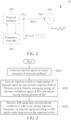
- FIG. 1 is a diagram illustrating a concept regarding startup (e.g. fast startup) of a crystal oscillator (XO) with aid of external clock injection according to an embodiment not covered by the present invention.
- XO crystal oscillator
- performance related to noise e.g. phase noise
- startup time required by the high-Q oscillator may be much greater than startup time required by the low-Q oscillator.
- the high-Q oscillator may include, but are not limited to: a Pierce XO and a Colpitts XO.
- Examples of the low-Q oscillator may include, but are not limited to: a ring oscillator and a resistor-capacitor (RC) oscillator.
- a fast startup technique shown in FIG. 1 may turn on injection switches coupled between the low-Q oscillator and the high-Q oscillator during a period T INJ , and inject energy of an injected signal V INJ of the low-Q oscillator into the high-Q oscillator (e.g. an XO 10 comprising an active device 11 (with a transconductance G m and a load capacitor C L therein), capacitors C m and C o , a resistor R m and an inductance L m ), thereby increasing energy (e.g.
- an XO 10 comprising an active device 11 (with a transconductance G m and a load capacitor C L therein), capacitors C m and C o , a resistor R m and an inductance L m ), thereby increasing energy (e.
- V m,ss and I m,ss of an intrinsic oscillation signal of the high-Q oscillator during a startup process of the XO, in order to accelerate the startup of the XO and allow the XO to output the intrinsic oscillation signal.
- an injection frequency of the low-Q oscillator is usually different from an intrinsic frequency of the high-Q oscillator at the beginning of the startup process, e.g. ⁇ 6000 parts per million (ppm), and therefore phase error between the injected signal and the intrinsic oscillation signal may be gradually accumulated.
- the fast startup technique shown in FIG. 1 may further utilize a feedback control mechanism, which detects the intrinsic frequency and accordingly modify the low-Q oscillator, in order to make the injection frequency approach the intrinsic frequency.
- the injection switch may be turned on during a first injection period, and energy of the intrinsic oscillation signal may increase, where the injected signal may dominate an overall waveform (e.g.
- the injection switch is then turned off during a lock/synchronization period following the first injection period, to allow the intrinsic frequency to be detected for controlling the low-Q oscillator. After the injection frequency approaches the intrinsic frequency, the injection switch is turned on again during a second injection period following the lock/synchronization period, and the clock injection proceeds.
- FIG. 2 is a diagram illustrating an XO 20 according to an embodiment of the present invention.
- the XO 20 may comprise an XO core circuit 100, an external oscillator 200 of the XO core circuit 100 (in particular, the external oscillator 200 is positioned outside the XO core circuit 100), at least one injection switch (e.g.
- a quality factor of the external oscillator 200 is lower than a quality factor of the XO core circuit 100, where the XO core circuit 100 may be an example of the high-Q oscillator, and the external oscillator 200 may be an example of the low-Q oscillator.
- FIG. 3 is a flowchart illustrating a method for startup of the XO 20 shown in FIG. 2 with aid of external clock injection according to an embodiment of the present invention. It should be noted that the working flow shown in FIG. 3 is for illustrative purposes only, and is not a limitation of the present invention. One or more steps may be added, deleted or modified in the working flow shown in FIG. 3 . In addition, if a same result may be obtained, these steps do not have to be executed in the exact order shown in FIG. 3 . For better comprehension, please refer to FIG. 3 in conjunction with FIG. 2 .
- the external oscillator 200 may generate an injected signal (e.g. a low-Q signal) within the external oscillator 200.
- an operating frequency of the frequency controller 300 is controlled by the external oscillator (e.g. the operating frequency of the frequency controller 300 may be equal to an injection frequency of the injected signal), but the present invention is not limited thereto.
- a system comprising the XO 20 may utilize the signal INJ EN to turn on the injection switch to make energy of the injected signal be injected into the XO core circuit 100, thereby increasing energy (e.g. energy I m (t) of a resonator) of an intrinsic oscillation signal of the XO core circuit 100 during a startup process of the XO 20.
- energy e.g. energy I m (t) of a resonator
- both the injected signal and the intrinsic oscillation signal may exist at the injection node N INJ , and an amplitude modulation (AM) signal is generated on the injection node N INJ according to combination of the injected signal and the intrinsic oscillation signal.
- the injected signal e.g. an output square wave
- the intrinsic oscillation signal may be modulated by the intrinsic oscillation signal to generate the AM signal, as illustrated by a waveform of a signal V GATE (t) shown in FIG. 1 .
- the frequency controller 300 may receive the AM signal and control the external oscillator 200 to selectively change the injection frequency of the injected signal according to the AM signal such as the waveform of the signal V GATE (t). More particularly, during the start-up process when the external oscillator selectively changes the injection frequency of the injected signal, the injection switch is always turned on (e.g., not turned off) or at least turned on for a duration.
- phase error e.g. phase error
- the injection frequency e.g. F INJ
- the intrinsic frequency e.g. F XO
- the waveform of the signal V GATE (t) may be regarded as a square wave from the external oscillator 200 being distorted by the intrinsic oscillation signal (which may be represented by I m (t)) from the XO core circuit 100, and different distortions (e.g. beating envelopes) may correspond to different relative phases between the injected signal and the intrinsic oscillation signal.
- the AM signal such as the signal V GATE (t).
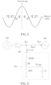
- FIG. 5 illustrates a relationship between a growth rate of the intrinsic oscillation signal and the relative phase according to an embodiment of the present invention.
- the growth rate of the intrinsic oscillation signal may be positive in response to the external clock injection; and when the relative phase falls outside this interval (e.g. the relative phase > +90° or the relative phase ⁇ -90°), the growth rate may be negative in response to the external clock injection, which means the low-Q oscillator may hinder the startup of the XO when the relative phase falls outside the interval between +90° and -90°.
- the injection switch is not turned off until the startup process is completed.
- the clock injection of the XO 20 is not interrupted for the lock/synchronization period required in the previous embodiment
- the information related to the relative phase can be extracted from the signal V GATE according to the distortions, for controlling the injection frequency.
- the frequency controller 300 can utilize a control mechanism to ensure the relative phase always falls in the interval between +90° and -90°, and thereby prevent the startup process from being hindered by the injected signal.
- efficiency of clock injection is improved, and the startup time can be greatly reduced.
- the frequency controller 300 shown in FIG. 2 may comprise a demodulation circuit, where the demodulation circuit may be configured to receive the AM signal and generate a sequence of demodulated voltages according to the AM signal.
- FIG. 6 is a diagram illustrating detailed implementation of generating the sequence of demodulated voltages by a demodulation circuit 310 according to an embodiment of the present invention, where the demodulation circuit 310 may be an example of the aforementioned demodulation circuit.
- the external oscillator 200 shown in FIG. 2 may comprise a low-Q oscillator 210 (e.g. a ring oscillator or an RC oscillator) and at least one output buffer (e.g.
- an output buffer 220 shown in FIG. 6 , where the buffer 220 may be coupled between the low-Q oscillator 210 and the injection node N INJ .
- the buffer 220 may be omitted.
- the demodulation circuit 310 may be implemented by using a diode with sample and hold mechanism as shown in FIG. 6 , to extract the information related to the relative phase (e.g. the beating envelopes) from the AM signal such as the signal V GATE (t).
- the demodulation circuit 310 may comprise a diode D0, a reset switch controlled by a signal RST, a sampling switch controlled by a signal RSTB and a sampling capacitor C S , where a cathode of the diode D0 is coupled to a sampling node of the demodulation circuit 310, the reset switch is coupled between the sampling node and a reference terminal (e.g.
- the sampling switch is coupled between an anode of the diode D0 and the injection node N INJ (or coupled between the anode of the diode D0 and the output terminal N OUT of the XO core circuit 100 in other embodiments), and the sampling capacitor C S is coupled between the sampling node and the reference terminal.
- a voltage level of the sampling node is reset to a reference level of the reference terminal; and when the reset switch is turned off and the sampling switch is turned on during a sampling period, charges are accumulated on the sampling node in response to a voltage level of the AM signal exceeding a threshold corresponding to the diode D0 (e.g. in response to the voltage level of the signal V GATE (t) making a voltage difference between the cathode and the anode of the diode D0 greater than a threshold voltage of the diode D0), to generate a demodulated voltage of the sequence of demodulated voltages on the sampling node.
- the operations of the demodulation circuit 310 is similar to an integrator, so information related to the distortions may correspond to the sequence of demodulated voltages, where the sequence of demodulated voltages may be represented by a signal V De-MOD . Note that each demodulated voltage of the sequence of demodulated voltages is generated through the same diode (i.e. the diode D0), and no mismatch issue is introduced among the sequence of demodulated voltages.
- FIG. 7 illustrates some details of a relationship between the relative phase and the distortions (e.g. the beating envelopes) according to an embodiment of the present invention.
- the energy of the intrinsic oscillation signal such as a signal Vxo (e.g. amplitude of the signal Vxo) is unchanged.
- the beating envelopes which is represented by Env1( ⁇ ) may be 0, ⁇ 2 A 0 , -2 A 0 , ⁇ 2 A 0 , and 0 when ⁇ is -90°, -45°, 0°, +45° and +90°, respectively, where A 0 may represent amplitude of the signal Vxo.
- a relative phase ⁇ min that results in a minimized beating envelope Env1( ⁇ ) may be 0°.
- the energy of the intrinsic oscillation signal such as the signal Vxo may grow over time as shown in FIG. 9 .
- the beating envelopes with growing amplitude of the signal Vxo may be represented by Env1( ⁇ ).
- the beating envelopes Env1( ⁇ ) may be 0, ⁇ 2 A 0 + k ⁇ , k ⁇ ], and 0 when ⁇ is -90°, -45°, 0°, +45° and +90°, respectively, where k may represent a growth rate of the amplitude of the signal Vxo.
- the relative phase ⁇ when the relative phase ⁇ accumulates in a positive direction, the relative phase ⁇ min that results in a minimized beating envelope Env1( ⁇ ) may fall in an interval between 0° and 90° when A 0 and k are positive values.
- the relative phase ⁇ accumulates in a negative direction
- the relative phase ⁇ m ⁇ n that results in a minimized beating envelope Env1( ⁇ ) may fall in an interval between 0° and -90° when A 0 and k are positive values.
- a relative phase between the injected signal and the intrinsic oscillation signal which results that a minimum voltage (more particularly, a local minimum voltage) within the sequence of demodulated voltages shows up, falls in an interval between +90° and -90°.
- FIG. 11 is a diagram illustrating a detailed implementation of the XO 20 according to an embodiment of the present invention. Note that the injection switch is turned on during the startup process, and is omitted in FIG. 11 for brevity.
- the frequency controller 300 shown in FIG. 3 may further comprise a monitoring circuit 320 coupled to the demodulation circuit, and a finite state machine (FSM) 330 (an FSM with counter) coupled to the monitoring circuit 320 and the external oscillator 200 (e.g. the low-Q oscillator 210).
- the FSM 330 may utilize the injected signal to be a counting clock (e.g.
- the monitoring circuit 320 may be configured to generate a monitored result according to the sequence of demodulated voltages, and the FSM 330 may be configured to control the external oscillator 200 (e.g. the low-Q oscillator 210) through a signal V control to selectively change the injection frequency according to the monitored result, to ensure the relative phase falls in an interval between +90 degrees and -90 degrees.
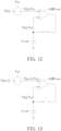
- the monitoring circuit 320 may comprise an amplifier AMP COMP , a capacitor C COMP and a loop switch controlled by a signal LOOP EN , where a first input terminal (which is labeled "+" on the amplifier AMP COMP shown in FIG.
- the amplifier AMP COMP may be coupled to the demodulation circuit 310 (e.g. the sampling node therein), the capacitor C COMP may be coupled between a reference terminal and a second input terminal (which is labeled "-" on the amplifier AMP COMP shown in FIG. 11 ) of the amplifier AMP COMP , and the loop switch may be coupled between the second input terminal and an output terminal of the amplifier AMP COMP .
- a D flip-flop (DFF) 322 controlled by the signal LOOP EN may be included in the monitoring circuit 320, where the DFF is coupled between the output terminal of the amplifier AMP COMP and the FSM 330 to make the FSM 330 receives digital results only, but the present invention is not limited thereto.
- DFF D flip-flop
- the amplifier AMP COMP may be configured to receive the sequence of demodulated voltages through the first input terminal thereof, the capacitor C COMP may be configured to sequentially store the sequence of demodulated voltages, and the loop switch is configured to control configurations of the monitoring circuit 320.
- FIGs. 12 and 13 where FIG. 12 illustrates operations of the monitoring circuit 320 shown in FIG. 11 during a preset phase, and FIG. 13 illustrates operations of the monitoring circuit 320 shown in FIG. 11 during an evaluation phase.
- the loop switch is turned on, the monitoring circuit 320 is configured as a unit gain buffer to transmit a first demodulated voltage within the sequence of demodulated voltages from the first input terminal of the amplifier AMP COMP to the capacitor C COMP (e.g. the second input terminal of the amplifier AMP COMP ).
- the monitoring circuit 320 is configured as a comparator to compare the second demodulated voltage on the first input terminal of the amplifier AMP COMP with the first demodulated voltage stored on the capacitor (on the second input terminal of the amplifier AMP COMP ), and accordingly generates a comparison result, wherein the monitored result comprises the comparison result.
- consecutive comparison results of the sequence of demodulated voltages may be generated, where these consecutive comparison results may represent the monitored result.
- a comparison result "0" of the monitoring circuit 320 indicates that a previous demodulated voltage of two consecutive demodulated voltages within the sequence of demodulated voltages (e.g. the aforementioned first demodulated voltage) is greater than a later demodulated voltage of these two consecutive demodulated voltages within the sequence of demodulated voltages (e.g. the aforementioned first demodulated voltage), and a comparison result "1" of the monitoring circuit 320 indicates that the previous demodulated voltage of these two consecutive demodulated voltages is less than the later demodulated voltage.
- the comparison result changes from "0" to "1” it means that the local minimum of the sequence of demodulated voltages is detected.
- an intrinsic offset Vos caused by mismatch of the first input terminal and the second input terminal of the amplifier AMP COMP may exist. Based on the operations shown in FIG. 12 and FIG 13 , impact from the intrinsic offset V OS may be removed from the comparison result.
- the first demodulated voltage (which may be represented by "V[n]") is transmitted to the second input terminal of the amplifier AMP COMP from the first input terminal of the amplifier AMP COMP during the preset phase
- the intrinsic offset Vos can be stored on the capacitor C COMP in conjunction with the first voltage, so the capacitor C COMP may store a voltage V[n] - Vos; and during the evaluation phase, the second demodulated voltage (which may be represented by V[n+1]) may exist on the first terminal of the amplifier AMP COMP in conjunction with the intrinsic offset Vos.
- the comparison result e.g. AD RESULT shown in FIG. 13
- the comparison result (e.g. AD RESULT shown in FIG. 13 ) will not be affected by the intrinsic offset.
- the monitoring circuit 320 is not limited to being used in the XO 20 shown in 11. Any system that required consecutive comparison operations (e.g. generate a comparison result regarding adjacent data (or voltages) within a sequence of data (or voltages)) may be implemented by the monitoring circuit 320.
- the diode D0 within the demodulation circuit 310 may be replaced with a transistor M0 (e.g. an N-type transistor) as shown in FIG. 14 , where a gate terminal of the transistor M0 is coupled to the drain terminal of the transistor M0, to make the transistor act like a diode, but the present invention is not limited thereto.
- the injection switch is turned on during the startup process, and is omitted in FIG. 11 for brevity.
- the monitoring circuit 320 may be replaced with a monitoring circuit 320A as illustrated by an XO 30 shown in FIG. 15 , where the monitoring circuit 320A may comprise a comparator COMP, a first sampling switch controlled by a signal SH, a second sampling switch controlled by a signal SHB, a first sampling capacitor C 1 and a second sampling capacitor C 2 .
- the injection switch is turned on during the startup process, and is omitted in FIG. 11 for brevity. As shown in FIG.
- the first sampling switch and the first sampling capacitor C 1 forms a first sample and hold circuit coupled to a first input terminal (which labeled "+” on the comparator COMP) of the comparator COMP
- the second sampling switch and the second sampling capacitor C 2 forms a second sample and hold circuit coupled to a second input terminal (which labeled "+” on the comparator COMP) of the comparator COMP, where signals VA and VB represent voltage on the first input terminal and the second input terminal of the comparator COMP.
- FIG. 16 is a timing diagram illustrating some signals (e.g. the counting clock CLK counting , the signals RST, RSTB, SH, SHB, and the signals VA and VB) within the XO 20 shown in FIG. 15 according to an embodiment of the present invention.
- the signals RST, RSTB, SH and SHB may be generated by a timing controller (not shown) according to the counting clock CLK counting , but the present invention is not limited thereto.
- each of the sequence of demodulated voltages may be sampled on either the sampling capacitor C 1 or C 2 by turns, and corresponding monitored result of the sequence of demodulated voltages may be output from the comparator COMP.
- the monitoring circuit 320 may be replaced with an analog-to-digital converter (ADC) 320B as illustrated by an XO 40 shown in FIG. 17 .
- ADC analog-to-digital converter
- the injection switch is turned on during the startup process, and is omitted in FIG. 11 for brevity.
- the ADC 320B may sequentially convert the sequence of demodulated voltages into digital codes, where these digital codes may represent the aforementioned monitored result, and the FSM 330 may control the low-Q oscillator 210 to selectively change the injection frequency according to these digital codes.
- FIG. 18 illustrates some details related to control of the injection frequency according to an embodiment of the present invention.
- the FSM 330 may control the external oscillator (e.g. the low-Q oscillator 210) to iteratively switch the injection frequency to one or more target frequency among multiple candidate frequencies according to the monitored result, to make the injection frequency stepwise approach the intrinsic frequency of the intrinsic oscillation signal, wherein the multiple candidate frequencies corresponds to multiple states of the FSM 330, respectively.
- the intrinsic frequency (which may be regarded as a target frequency) is equal to a center frequency among the multiple candidate frequencies (e.g. having 0ppm frequency error relative to the center frequency).
- the relative phase e.g. phase error
- the relative phase may start accumulating in the positive direction, where the energy of the intrinsic oscillation signal is increasing, and levels of the sequence of demodulated voltage such as the signal V De-MOD is decreasing, so the comparison result from the monitoring circuit 320 is kept at "0" at the beginning.
- the monitored result indicates that a later demodulated voltage is greater than a previous demodulated voltage at a time point t1 (e.g.
- the comparison result from the monitoring circuit 320 changes from "0" to "1"
- the FSM 330 may determine that candidate frequencies greater than the second frequency is not available, and control the external oscillator 200 (e.g.
- the low-Q oscillator to switch the injection frequency from the second frequency to a third frequency which has -4000ppm frequency error relative to the center frequency.
- the injection frequency may be switched to a fourth frequency, a fifth frequency, a sixth frequency and a seventh frequency at time points t3, t4, t5 and t6, respectively. Similar descriptions are not repeated here for brevity. According to this, whenever a demodulated voltage within the sequence of the demodulated voltages reaches a minimum, the injection frequency can be adjusted properly, such that the relative phase may accumulate in alternating directions, and thereby ensure that the relative phase is confined within ⁇ 90° (typically, within ⁇ 40° or less), so the energy of the intrinsic oscillation signal always increases.
- FIG. 19 illustrates some details related to control of the injection frequency according to another embodiment of the present invention.
- the intrinsic frequency which may be regarded as a target frequency
- the monitored result indicates that the comparison result changes from "0" to "1" at a time point t7 (i.e. a demodulated voltage V1 is greater than a demodulated voltage V2)
- the FSM 330 may determine that candidate frequencies less than the third frequency (which has -4000ppm frequency error) is not available, and control the external oscillator 200 (e.g.
- the FSM 330 may control the external oscillator 200 (e.g. the low-Q oscillator) to further switch the injection frequency from the fourth frequency to an eighth frequency (which has +4500ppm frequency error) greater than the fourth frequency (which has +4000ppm frequency error) in order to change the accumulating direction of the relative phase.
- the FSM 330 may control the external oscillator 200 (e.g. the low-Q oscillator) to further switch the injection frequency from the tenth frequency to an eleventh frequency less than the tenth frequency.
- the external oscillator 200 e.g. the low-Q oscillator
- the FSM 330 may control the external oscillator 200 (e.g. the low-Q oscillator 210) to iteratively switch the injection frequency to either a first candidate frequency (e.g. the first frequency having -5000ppm frequency error) or a second candidate frequency (e.g. the second frequency having +5000ppm frequency error) according to the monitored result.
- a first candidate frequency e.g. the first frequency having -5000ppm frequency error
- a second candidate frequency e.g. the second frequency having +5000ppm frequency error
- the injection switch may be turned on for a predetermined time period. That is, the time point to turn off the injection switch (or the timing to finish the startup process) may be determined in advance.
- the system comprising the XO 20 may monitor at least one signal within the XO 20, to trigger the system to finish the startup process (e.g. turn off the injection switch) in response to the aforementioned at least one signal satisfying a specific condition.
- an initial demodulated voltage represents a first demodulated voltage of the sequence of demodulated voltages at the beginning of the startup process
- the system may determine that the startup process is completed, and the injection switch may be turned off, wherein a voltage difference between the target demodulated voltage and the initial demodulated voltage is greater than or equal to a predetermined value.
- the startup process may be regarded as completed, and the injection switch is therefore turned off.
- the startup method and associated XO architecture can control the switching of the injection frequency according to the distorted square wave caused by amplitude modulation of the injected signal and the intrinsic oscillation signal, to make the relative phase between the injected signal and the intrinsic oscillation signal confined within a desired interval (e.g. ⁇ 90°). Based on this, the injection switch does not need to be turned off for the aforementioned lock/synchronization period, and it is further ensured that the energy of the intrinsic oscillation signal always increases. Assume that a reference time period is required for the startup process when the injected frequency of the injected signal is identical to the intrinsic frequency of the XO core circuit.
- a 17.4 to 90.6 times the reference time period might be required for the startup process.
- a 1.05 to 1.5 times the reference time period may be required, which means the present invention indeed greatly enhance clock injection efficiency, and the startup time can be greatly reduced.
Landscapes
- Physics & Mathematics (AREA)
- General Physics & Mathematics (AREA)
- Nonlinear Science (AREA)
- Oscillators With Electromechanical Resonators (AREA)
- Stabilization Of Oscillater, Synchronisation, Frequency Synthesizers (AREA)
Claims (14)
- Verfahren zum Starten eines Kristalloszillators, XO, (10, 20, 30) mit Hilfe einer externen Taktinjektion, wobei das Verfahren Folgendes umfasst:Verwenden eines externen Oszillators (200), der sich außerhalb einer XO-Kernschaltung (100) des XO (10, 20, 30) befindet, um ein injiziertes Signal zu generieren, wobei der XO (10, 20, 30) die XO-Kernschaltung (100) umfasst und der externe Oszillator (200) außerhalb der XO-Kernschaltung (100) positioniert ist, und mindestens eines Injektionsschalters, wobei der mindestens eine Injektionsschalter zwischen einen Injektionsknoten des XO (10, 20, 30) und einen Ausgangsanschluss der XO-Kernschaltung (100) gekoppelt ist, der externe Oszillator (200) an den Injektionsknoten gekoppelt ist und ein Qualitätsfaktor des externen Oszillators (200) geringer als ein Qualitätsfaktor der XO-Kernschaltung (100) ist;Einschalten des mindestens einen Injektionsschalters, damit Energie des injizierten Signals in die XO-Kernschaltung (100) injiziert wird, wodurch die Energie eines intrinsischen Oszillationssignals der XO-Kernschaltung (100) erhöht wird, wobei ein Modulationssignal an dem Injektionsknoten gemäß einer Kombination des injizierten Signals und des intrinsischen Oszillationssignals generiert wird; undSteuern des externen Oszillators (200), um eine Injektionsfrequenz des injizierten Signals gemäß dem Modulationssignal selektiv zu ändern;wobei der mindestens eine Injektionsschalter eingeschaltet ist, während der externe Oszillator (200) die Injektionsfrequenz des injizierten Signals selektiv ändert.
- Verfahren nach Anspruch 1, wobei der Schritt des Steuerns des externen Oszillators (200), um die Injektionsfrequenz des injizierten Signals gemäß dem Modulationssignal selektiv zu ändern, Folgendes umfasst:Verwenden einer Demodulationsschaltung (310) des XO (10, 20, 30), um eine Sequenz von demodulierten Spannungen gemäß dem Modulationssignal zu generieren, wobei die Sequenz von demodulierten Spannungen Informationen über eine relative Phase zwischen dem injizierten Signal und dem intrinsischen Oszillationssignal enthält;Verwenden einer Überwachungsschaltung (320) des XO (10, 20, 30), um ein überwachtes Ergebnis gemäß der Sequenz von demodulierten Spannungen zu generieren; undSteuern des externen Oszillators (200), um die Injektionsfrequenz gemäß dem überwachten Ergebnis selektiv zu ändern.
- Verfahren nach Anspruch 2, wobei der Schritt des Steuerns des externen Oszillators (200), um die Injektionsfrequenz gemäß dem überwachten Ergebnis selektiv zu ändern, Folgendes umfasst:iteratives Umschalten der Injektionsfrequenz entweder auf eine erste Frequenz oder eine zweite Frequenz gemäß dem überwachten Ergebnis, um zu bewirken, dass die relative Phase in ein Intervall zwischen +90 Grad und -90 Grad fällt, wobei die erste Frequenz größer als eine intrinsische Frequenz des intrinsischen Oszillationssignals ist und die zweite Frequenz geringer als die intrinsische Frequenz ist; oderwobei der Schritt des Steuerns des externen Oszillators (200), um die Injektionsfrequenz gemäß dem überwachten Ergebnis selektiv zu ändern, Folgendes umfasst:
Umschalten der Injektionsfrequenz zwischen mehreren Kandidatenfrequenzen gemäß dem überwachten Ergebnis, damit sich die Injektionsfrequenz an eine intrinsische Frequenz des intrinsischen Oszillationssignals annähert, wobei die mehreren Kandidatenfrequenzen jeweils mehreren Zuständen einer endlichen Zustandsmaschine (finite state machine - FSM) (330) entsprechen. - Verfahren nach Anspruch 2, wobei die Sequenz von demodulierten Spannungen eine erste demodulierte Spannung und eine zweite demodulierte Spannung, die auf die erste demodulierte Spannung folgt, umfasst und der Schritt des Steuerns des externen Oszillators (200), um die Injektionsfrequenz gemäß dem überwachten Ergebnis selektiv zu ändern, Folgendes umfasst:
als Reaktion darauf, dass das überwachte Ergebnis angibt, dass die zweite demodulierte Spannung höher als die erste demodulierte Spannung ist, Umschalten der Injektionsfrequenz von einer ersten Frequenz auf eine zweite Frequenz. - Verfahren nach Anspruch 4, wobei die Sequenz von demodulierten Spannungen ferner eine dritte demodulierte Spannung, die auf die zweite demodulierte Spannung folgt, umfasst und der Schritt des Steuerns des externen Oszillators (200), um die Injektionsfrequenz gemäß dem überwachten Ergebnis selektiv zu ändern, Folgendes umfasst:als Reaktion darauf, dass das überwachte Ergebnis angibt, dass die dritte demodulierte Spannung höher als die zweite demodulierte Spannung ist, Umschalten der Injektionsfrequenz von der zweiten Frequenz auf eine dritte Frequenz;wobei die erste Frequenz größer als die zweite Frequenz ist und die zweite Frequenz größer als die dritte Frequenz ist; oder die erste Frequenz geringer als die zweite Frequenz ist und die zweite Frequenz geringer als die dritte Frequenz ist.
- Verfahren nach Anspruch 2, wobei die Sequenz von demodulierten Spannungen eine erste demodulierte Spannung und eine zweite demodulierte Spannung, die auf die erste demodulierte Spannung folgt, umfasst, die Überwachungsschaltung (320) einen Verstärker und einen Kondensator umfasst und der Schritt des Verwendens der Überwachungsschaltung (320), um das überwachte Ergebnis gemäß der Sequenz von demodulierten Spannungen zu generieren, Folgendes umfasst:Konfigurieren der Überwachungsschaltung (320) als Einheitsverstärkungspuffer, um die erste demodulierte Spannung von einem ersten Eingangsanschluss des Verstärkers an einen Kondensator, der an einen zweiten Eingangsanschluss des Verstärkers gekoppelt ist, zu übertragen, indem ein zwischen den zweiten Eingangsanschluss und einen Ausgangsanschluss des Verstärkers gekoppelter Loop-Schalter eingeschaltet wird; undKonfigurieren der Überwachungsschaltung (320) als Komparator, um die zweite demodulierte Spannung am ersten Eingangsanschluss des Verstärkers mit der ersten demodulierten Spannung, die durch Ausschalten des Loop-Schalters an dem Kondensator gespeichert ist, zu vergleichen und dementsprechend ein Vergleichsergebnis zu generieren, wobei das überwachte Ergebnis das Vergleichsergebnis umfasst;
oderwobei der Schritt des Verwendens der Demodulationsschaltung (310) zum Generieren der Sequenz von demodulierten Spannungen gemäß dem Modulationssignal Folgendes umfasst:Einschalten eines Rücksetzschalters der Demodulationsschaltung (310) und Ausschalten eines Abtastschalters der Demodulationsschaltung (310), um einen Spannungspegel eines Abtastknotens der Demodulationsschaltung (310) während einer Rücksetzperiode auf einen Referenzpegel zurückzusetzen; undAusschalten des Rücksetzschalters und Einschalten des Abtastschalters, um als Reaktion darauf, dass ein Spannungspegel des Modulationssignals während einer Abtastperiode einen einer Diode der Demodulationsschaltung (310) entsprechenden Schwellenwert überschreitet, Ladungen an dem Abtastknoten zu akkumulieren, um eine demodulierte Spannung der Sequenz von demodulierten Spannungen an dem Abtastknoten zu generieren; oderwobei eine anfängliche demodulierte Spannung eine erste demodulierte Spannung der Sequenz von demodulierten Spannungen darstellt und das Verfahren ferner Folgendes umfasst:
als Reaktion darauf, dass erkannt wird, dass eine demodulierte Zielspannung der Sequenz von demodulierten Spannungen angibt, dass der Startvorgang abgeschlossen ist, Ausschalten des mindestens einen Injektionsschalters, wobei eine Spannungsdifferenz zwischen der demodulierten Zielspannung und der anfänglichen demodulierten Spannung größer als ein vorbestimmter Wert oder gleich diesem ist. - Kristalloszillator, XO, (10, 20, 30), umfassend:eine XO-Kernschaltung (100), die dazu konfiguriert ist, ein intrinsisches Oszillationssignal zu generieren;einen externen Oszillator (200), der an einen Injektionsknoten des XO (10, 20, 30) gekoppelt und dazu konfiguriert ist, ein injiziertes Signal zu generieren, wobei ein Qualitätsfaktor des externen Oszillators (200) geringer als ein Qualitätsfaktor des XO-Kernschaltung (100) ist;mindestens einen Injektionsschalter, der zwischen den Injektionsknoten und einen Ausgangsanschluss der XO-Kernschaltung (100) gekoppelt ist, wobei, wenn der mindestens eine Injektionsschalter eingeschaltet ist, Energie des injizierten Signals in die XO-Kernschaltung (100) injiziert wird, um die Energie des intrinsischen Oszillationssignals zu erhöhen, und ein Modulationssignal am Injektionsknoten gemäß einer Kombination des injizierten Signals und des intrinsischen Oszillationssignals generiert wird; undeine Frequenzsteuerung, die an den externen Oszillator (200) gekoppelt und dazu konfiguriert ist, den externen Oszillator (200) zu steuern, um eine Injektionsfrequenz des injizierten Signals gemäß dem Modulationssignal selektiv zu ändern;wobei der mindestens eine Injektionsschalter eingeschaltet ist, während der externe Oszillator (200) die Injektionsfrequenz des injizierten Signals selektiv ändert.
- XO (10, 20, 30) nach Anspruch 7, wobei die Frequenzsteuerung Folgendes umfasst:eine Demodulationsschaltung (310), die dazu konfiguriert ist, das Modulationssignal zu empfangen und eine Sequenz von demodulierten Spannungen gemäß dem Modulationssignal zu generieren, wobei die Sequenz von demodulierten Spannungen Informationen über eine relative Phase zwischen dem injizierten Signal und dem intrinsischen Oszillationssignal enthält;eine Überwachungsschaltung (320), die an die Demodulationsschaltung (310) gekoppelt und dazu konfiguriert ist, ein überwachtes Ergebnis gemäß der Sequenz von demodulierten Spannungen zu generieren; undeine endliche Zustandsmaschine, FSM, (330), die an die überwachte Schaltung und den externen Oszillator (200) gekoppelt und dazu konfiguriert ist, den externen Oszillator (200) zu steuern, um die Injektionsfrequenz gemäß dem überwachten Ergebnis selektiv zu ändern.
- XO (10, 20, 30) nach Anspruch 8, wobei die FSM (330) den externen Oszillator (200) steuert, um die Injektionsfrequenz gemäß dem überwachten Ergebnis entweder auf eine erste Frequenz oder eine zweite Frequenz iterativ umzuschalten, um zu bewirken, dass die relative Phase in ein Intervall zwischen +90 Grad und -90 Grad fällt, wobei die erste Frequenz größer als eine intrinsische Frequenz des intrinsischen Oszillationssignals ist und die zweite Frequenz geringer als die intrinsische Frequenz ist;
oder
wobei die FSM (330) den externen Oszillator (200) steuert, um die Injektionsfrequenz gemäß dem überwachten Ergebnis zwischen mehreren Kandidatenfrequenzen umzuschalten, damit sich die Injektionsfrequenz an eine intrinsische Frequenz des intrinsischen Oszillationssignals annähert, wobei die mehreren Kandidatenfrequenzen jeweils mehreren Zuständen der FSM (330) entsprechen. - XO (10, 20, 30) nach Anspruch 8, wobei die Sequenz von demodulierten Spannungen eine erste demodulierte Spannung und eine zweite demodulierte Spannung, die auf die erste demodulierte Spannung folgt, umfasst; und wenn das überwachte Ergebnis angibt, dass die zweite demodulierte Spannung höher als die erste demodulierte Spannung ist, die FSM (330) den externen Oszillator (200) steuert, um die Injektionsfrequenz von einer ersten Frequenz auf eine zweite Frequenz umzuschalten.
- XO (10, 20, 30) nach Anspruch 10, wobei die Sequenz von demodulierten Spannungen ferner eine dritte demodulierte Spannung, die auf die zweite demodulierte Spannung folgt, umfasst; und wenn das überwachte Ergebnis angibt, dass die dritte demodulierte Spannung höher als die zweite demodulierte Spannung ist, die FSM (330) den externen Oszillator (200) steuert, um die Injektionsfrequenz von der zweiten Frequenz auf eine dritte Frequenz umzuschalten; wobei die erste Frequenz größer als die zweite Frequenz ist und die zweite Frequenz größer als die dritte Frequenz ist; oder die erste Frequenz geringer als die zweite Frequenz ist und die zweite Frequenz geringer als die dritte Frequenz ist.
- XO (10, 20, 30) nach Anspruch 8, wobei die Sequenz von demodulierten Spannungen eine erste demodulierte Spannung und eine zweite demodulierte Spannung, die auf die erste demodulierte Spannung folgt, umfasst und die Überwachungsschaltung (320) Folgendes umfasst:einen Verstärker, der an die Demodulationsschaltung (310) gekoppelt und dazu konfiguriert ist, die Sequenz von demodulierten Spannungen über einen ersten Eingangsanschluss des Verstärkers zu empfangen;einen Kondensator, der an einen zweiten Eingangsanschluss des Verstärkers gekoppelt und dazu konfiguriert ist, die Sequenz von demodulierten Spannungen sequentiell zu speichern; undeinen Loop-Schalter, der zwischen den zweiten Eingangsanschluss und einen Ausgangsanschluss des Verstärkers gekoppelt und dazu konfiguriert ist, Konfigurationen der Überwachungsschaltung (320) zu steuern;wobei, wenn der Loop-Schalter eingeschaltet ist, die Überwachungsschaltung (320) als Einheitsverstärkungspuffer konfiguriert ist, um die erste demodulierte Spannung von dem ersten Eingangsanschluss des Verstärkers an den Kondensator zu übertragen; und wenn der Loop-Schalter ausgeschaltet ist, die Überwachungsschaltung (320) als Komparator konfiguriert ist, um die zweite demodulierte Spannung am ersten Eingangsanschluss des Verstärkers mit der ersten demodulierten Spannung, die an dem Kondensator gespeichert ist, zu vergleichen und dementsprechend ein Vergleichsergebnis generiert, wobei das überwachte Ergebnis das Vergleichsergebnis umfasst.
- XO (10, 20, 30) nach Anspruch 8, wobei die Demodulationsschaltung (310) Folgendes umfasst:eine Diode, deren Kathode an einen Abtastknoten der Demodulationsschaltung (310) gekoppelt ist;einen Rücksetzschalter, der zwischen den Abtastknoten und einen Referenzanschluss der Demodulationsschaltung (310) gekoppelt ist;einen Abtastschalter, der an eine Anode der Diode gekoppelt ist; undeinen Abtastkondensator, der an den Abtastknoten gekoppelt ist; wobei, wenn während einer Rücksetzperiode der Rücksetzschalter eingeschaltet und der Abtastschalter ausgeschaltet ist, ein Spannungspegel des Abtastknotens auf einen Referenzpegel des Referenzanschlusses zurückgesetzt wird; und wenn während einer Abtastperiode der Rücksetzschalter ausgeschaltet und der Abtastschalter eingeschaltet ist, Ladungen an dem Abtastknoten als Reaktion darauf, dass ein Spannungspegel des Modulationssignals einen der Diode entsprechenden Schwellenwert überschreitet, akkumuliert werden, um eine demodulierte Spannung der Sequenz von demodulierten Spannungen an dem Abtastknoten zu generieren.
- XO (10, 20, 30) nach Anspruch 8, wobei eine anfängliche demodulierte Spannung eine erste demodulierte Spannung der Sequenz von demodulierten Spannungen darstellt; und wenn erkannt wird, dass eine demodulierte Zielspannung der Sequenz von demodulierten Spannungen angibt, dass der Startvorgang abgeschlossen ist, der mindestens eine Injektionsschalter ausgeschaltet wird, wobei eine Spannungsdifferenz zwischen der demodulierten Zielspannung und der anfänglichen demodulierten Spannung größer als ein vorbestimmter Wert oder gleich diesem ist.
Applications Claiming Priority (2)
| Application Number | Priority Date | Filing Date | Title |
|---|---|---|---|
| US201962905579P | 2019-09-25 | 2019-09-25 | |
| US17/026,275 US11183971B2 (en) | 2019-09-25 | 2020-09-20 | Method for startup of crystal oscillator with aid of external clock injection, associated crystal oscillator and monitoring circuit therein |
Publications (3)
| Publication Number | Publication Date |
|---|---|
| EP3799298A2 EP3799298A2 (de) | 2021-03-31 |
| EP3799298A3 EP3799298A3 (de) | 2021-06-02 |
| EP3799298B1 true EP3799298B1 (de) | 2023-11-08 |
Family
ID=72659016
Family Applications (1)
| Application Number | Title | Priority Date | Filing Date |
|---|---|---|---|
| EP20198139.6A Active EP3799298B1 (de) | 2019-09-25 | 2020-09-24 | Verfahren zum starten eines kristalloszillators mit hilfe einer externen taktinjektion und zugehöriger kristalloszillator |
Country Status (2)
| Country | Link |
|---|---|
| US (1) | US11183971B2 (de) |
| EP (1) | EP3799298B1 (de) |
Families Citing this family (1)
| Publication number | Priority date | Publication date | Assignee | Title |
|---|---|---|---|---|
| CN115800927B (zh) * | 2023-01-31 | 2023-04-25 | 南京邮电大学 | 一种基于占空比检测的晶体振荡器 |
Family Cites Families (14)
| Publication number | Priority date | Publication date | Assignee | Title |
|---|---|---|---|---|
| US5625304A (en) | 1995-04-21 | 1997-04-29 | Lucent Technologies Inc. | Voltage comparator requiring no compensating offset voltage |
| US6819195B1 (en) | 2003-03-07 | 2004-11-16 | Ami Semiconductor, Inc. | Stimulated quick start oscillator |
| JP2006322711A (ja) | 2005-05-17 | 2006-11-30 | Fuji Electric Device Technology Co Ltd | 電圧検出回路および電流検出回路 |
| US7482888B1 (en) | 2007-07-12 | 2009-01-27 | Zerog Wireless, Inc. | Fast startup resonant element oscillator |
| US7579919B1 (en) | 2007-10-13 | 2009-08-25 | Weixun Cao | Method and apparatus for compensating temperature changes in an oscillator-based frequency synthesizer |
| JP5737834B2 (ja) | 2008-08-23 | 2015-06-17 | シーウェア・システムズSi−Ware Systems | 正確で安定したlc型基準発振器のための方法、システム、および装置 |
| CN104272538B (zh) | 2012-03-27 | 2017-03-01 | 光电波股份有限公司 | 具有运行于选定调制边带上的光学谐振滤波器的可调谐光电振荡器 |
| US9515603B2 (en) * | 2014-10-14 | 2016-12-06 | Cypress Semiconductor Corporation | Crystal oscillator start-up circuit |
| US9246435B1 (en) * | 2015-02-09 | 2016-01-26 | Qualcomm Incorporated | Method to pre-charge crystal oscillators for fast start-up |
| WO2016146154A1 (en) | 2015-03-13 | 2016-09-22 | Telefonaktiebolaget Lm Ericsson (Publ) | Reducing duration of start-up period for a crystal oscillator circuit |
| GB2560413A (en) | 2015-06-16 | 2018-09-12 | Nordic Semiconductor Asa | Voltage monitor |
| US10050585B2 (en) | 2015-06-18 | 2018-08-14 | Microchip Technology Incorporated | Ultra-low power crystal oscillator with adaptive self-start |
| US10439556B2 (en) | 2016-04-20 | 2019-10-08 | Microchip Technology Incorporated | Hybrid RC/crystal oscillator |
| EP3687063B1 (de) | 2019-01-24 | 2022-08-24 | Nxp B.V. | Kristalloszillatorschaltung und verfahren zum betrieb |
-
2020
- 2020-09-20 US US17/026,275 patent/US11183971B2/en active Active
- 2020-09-24 EP EP20198139.6A patent/EP3799298B1/de active Active
Also Published As
| Publication number | Publication date |
|---|---|
| US20210091720A1 (en) | 2021-03-25 |
| EP3799298A2 (de) | 2021-03-31 |
| EP3799298A3 (de) | 2021-06-02 |
| US11183971B2 (en) | 2021-11-23 |
Similar Documents
| Publication | Publication Date | Title |
|---|---|---|
| EP2951919B1 (de) | Digital gesteuerter injektionssynchronisierter oszillator | |
| US20190236426A1 (en) | An oscillation maintenance circuit with comparator-based pulse generation in half-duplex rfid transponders | |
| US20190058575A1 (en) | Automatic detection of change in pll locking trend | |
| US12289112B2 (en) | Phase-locked loop device | |
| US20080238505A1 (en) | System and method for an automatic coarse tuning of a voltage controlled oscillator in a phase-locked loop (PLL) | |
| US20100085123A1 (en) | Injection-locked clock multiplier | |
| US8354866B2 (en) | PLL start-up circuit | |
| EP3799298B1 (de) | Verfahren zum starten eines kristalloszillators mit hilfe einer externen taktinjektion und zugehöriger kristalloszillator | |
| US7616066B2 (en) | Oscillation device and controlling method therefor | |
| EP1676366A1 (de) | Mehrband-pll-anordnung und verfahren zur steuerung einer solchen anordnung | |
| US20110133795A1 (en) | Digital phase-locked loop with reduced loop delay | |
| CN102195643B (zh) | Pll装置 | |
| CN111371523B (zh) | 一种时钟信号处理装置和方法 | |
| KR20190081415A (ko) | 주입 동기 주파수 체배기 및 그의 주파수 체배 방법 | |
| US11387781B1 (en) | Fast start-up crystal oscillator and fast start-up method thereof | |
| WO2008144152A1 (en) | Injection-locked clock multiplier | |
| CN114257207B (zh) | 借助外部时钟注入启动晶体振荡器的方法,晶体振荡器及监视电路 | |
| US7911283B1 (en) | Low noise oscillator and method | |
| US11671056B2 (en) | Crystal oscillator and phase noise reduction method thereof | |
| US20030020514A1 (en) | Phase comparator circuit | |
| JP2010200064A (ja) | Pll回路、pll回路無線通信機、及びpll回路のロック検出方法 | |
| JP4882693B2 (ja) | ルビジウム原子発振器 | |
| KR100632673B1 (ko) | 위상고정루프의 락타임 조절 기능을 가지는 무선통신단말기 및 그 방법 | |
| US12267082B2 (en) | Frequency-regulated oscillator circuit | |
| JP2008271291A (ja) | Pll回路 |
Legal Events
| Date | Code | Title | Description |
|---|---|---|---|
| PUAI | Public reference made under article 153(3) epc to a published international application that has entered the european phase |
Free format text: ORIGINAL CODE: 0009012 |
|
| STAA | Information on the status of an ep patent application or granted ep patent |
Free format text: STATUS: THE APPLICATION HAS BEEN PUBLISHED |
|
| AK | Designated contracting states |
Kind code of ref document: A2 Designated state(s): AL AT BE BG CH CY CZ DE DK EE ES FI FR GB GR HR HU IE IS IT LI LT LU LV MC MK MT NL NO PL PT RO RS SE SI SK SM TR |
|
| AX | Request for extension of the european patent |
Extension state: BA ME |
|
| PUAL | Search report despatched |
Free format text: ORIGINAL CODE: 0009013 |
|
| AK | Designated contracting states |
Kind code of ref document: A3 Designated state(s): AL AT BE BG CH CY CZ DE DK EE ES FI FR GB GR HR HU IE IS IT LI LT LU LV MC MK MT NL NO PL PT RO RS SE SI SK SM TR |
|
| RIC1 | Information provided on ipc code assigned before grant |
Ipc: H03B 5/06 20060101AFI20210427BHEP Ipc: H03B 5/32 20060101ALI20210427BHEP Ipc: H03K 5/24 20060101ALI20210427BHEP |
|
| STAA | Information on the status of an ep patent application or granted ep patent |
Free format text: STATUS: REQUEST FOR EXAMINATION WAS MADE |
|
| 17P | Request for examination filed |
Effective date: 20211130 |
|
| RBV | Designated contracting states (corrected) |
Designated state(s): AL AT BE BG CH CY CZ DE DK EE ES FI FR GB GR HR HU IE IS IT LI LT LU LV MC MK MT NL NO PL PT RO RS SE SI SK SM TR |
|
| GRAP | Despatch of communication of intention to grant a patent |
Free format text: ORIGINAL CODE: EPIDOSNIGR1 |
|
| STAA | Information on the status of an ep patent application or granted ep patent |
Free format text: STATUS: GRANT OF PATENT IS INTENDED |
|
| INTG | Intention to grant announced |
Effective date: 20230503 |
|
| P01 | Opt-out of the competence of the unified patent court (upc) registered |
Effective date: 20230607 |
|
| GRAS | Grant fee paid |
Free format text: ORIGINAL CODE: EPIDOSNIGR3 |
|
| GRAA | (expected) grant |
Free format text: ORIGINAL CODE: 0009210 |
|
| STAA | Information on the status of an ep patent application or granted ep patent |
Free format text: STATUS: THE PATENT HAS BEEN GRANTED |
|
| AK | Designated contracting states |
Kind code of ref document: B1 Designated state(s): AL AT BE BG CH CY CZ DE DK EE ES FI FR GB GR HR HU IE IS IT LI LT LU LV MC MK MT NL NO PL PT RO RS SE SI SK SM TR |
|
| REG | Reference to a national code |
Ref country code: GB Ref legal event code: FG4D |
|
| REG | Reference to a national code |
Ref country code: CH Ref legal event code: EP |
|
| REG | Reference to a national code |
Ref country code: DE Ref legal event code: R096 Ref document number: 602020020620 Country of ref document: DE |
|
| REG | Reference to a national code |
Ref country code: IE Ref legal event code: FG4D |
|
| REG | Reference to a national code |
Ref country code: LT Ref legal event code: MG9D |
|
| REG | Reference to a national code |
Ref country code: NL Ref legal event code: MP Effective date: 20231108 |
|
| PG25 | Lapsed in a contracting state [announced via postgrant information from national office to epo] |
Ref country code: GR Free format text: LAPSE BECAUSE OF FAILURE TO SUBMIT A TRANSLATION OF THE DESCRIPTION OR TO PAY THE FEE WITHIN THE PRESCRIBED TIME-LIMIT Effective date: 20240209 |
|
| PG25 | Lapsed in a contracting state [announced via postgrant information from national office to epo] |
Ref country code: IS Free format text: LAPSE BECAUSE OF FAILURE TO SUBMIT A TRANSLATION OF THE DESCRIPTION OR TO PAY THE FEE WITHIN THE PRESCRIBED TIME-LIMIT Effective date: 20240308 |
|
| PG25 | Lapsed in a contracting state [announced via postgrant information from national office to epo] |
Ref country code: LT Free format text: LAPSE BECAUSE OF FAILURE TO SUBMIT A TRANSLATION OF THE DESCRIPTION OR TO PAY THE FEE WITHIN THE PRESCRIBED TIME-LIMIT Effective date: 20231108 |
|
| REG | Reference to a national code |
Ref country code: AT Ref legal event code: MK05 Ref document number: 1630537 Country of ref document: AT Kind code of ref document: T Effective date: 20231108 |
|
| PG25 | Lapsed in a contracting state [announced via postgrant information from national office to epo] |
Ref country code: NL Free format text: LAPSE BECAUSE OF FAILURE TO SUBMIT A TRANSLATION OF THE DESCRIPTION OR TO PAY THE FEE WITHIN THE PRESCRIBED TIME-LIMIT Effective date: 20231108 |
|
| PG25 | Lapsed in a contracting state [announced via postgrant information from national office to epo] |
Ref country code: AT Free format text: LAPSE BECAUSE OF FAILURE TO SUBMIT A TRANSLATION OF THE DESCRIPTION OR TO PAY THE FEE WITHIN THE PRESCRIBED TIME-LIMIT Effective date: 20231108 |
|
| PG25 | Lapsed in a contracting state [announced via postgrant information from national office to epo] |
Ref country code: ES Free format text: LAPSE BECAUSE OF FAILURE TO SUBMIT A TRANSLATION OF THE DESCRIPTION OR TO PAY THE FEE WITHIN THE PRESCRIBED TIME-LIMIT Effective date: 20231108 |
|
| PG25 | Lapsed in a contracting state [announced via postgrant information from national office to epo] |
Ref country code: NL Free format text: LAPSE BECAUSE OF FAILURE TO SUBMIT A TRANSLATION OF THE DESCRIPTION OR TO PAY THE FEE WITHIN THE PRESCRIBED TIME-LIMIT Effective date: 20231108 Ref country code: LT Free format text: LAPSE BECAUSE OF FAILURE TO SUBMIT A TRANSLATION OF THE DESCRIPTION OR TO PAY THE FEE WITHIN THE PRESCRIBED TIME-LIMIT Effective date: 20231108 Ref country code: IS Free format text: LAPSE BECAUSE OF FAILURE TO SUBMIT A TRANSLATION OF THE DESCRIPTION OR TO PAY THE FEE WITHIN THE PRESCRIBED TIME-LIMIT Effective date: 20240308 Ref country code: GR Free format text: LAPSE BECAUSE OF FAILURE TO SUBMIT A TRANSLATION OF THE DESCRIPTION OR TO PAY THE FEE WITHIN THE PRESCRIBED TIME-LIMIT Effective date: 20240209 Ref country code: ES Free format text: LAPSE BECAUSE OF FAILURE TO SUBMIT A TRANSLATION OF THE DESCRIPTION OR TO PAY THE FEE WITHIN THE PRESCRIBED TIME-LIMIT Effective date: 20231108 Ref country code: BG Free format text: LAPSE BECAUSE OF FAILURE TO SUBMIT A TRANSLATION OF THE DESCRIPTION OR TO PAY THE FEE WITHIN THE PRESCRIBED TIME-LIMIT Effective date: 20240208 Ref country code: AT Free format text: LAPSE BECAUSE OF FAILURE TO SUBMIT A TRANSLATION OF THE DESCRIPTION OR TO PAY THE FEE WITHIN THE PRESCRIBED TIME-LIMIT Effective date: 20231108 Ref country code: PT Free format text: LAPSE BECAUSE OF FAILURE TO SUBMIT A TRANSLATION OF THE DESCRIPTION OR TO PAY THE FEE WITHIN THE PRESCRIBED TIME-LIMIT Effective date: 20240308 |
|
| PG25 | Lapsed in a contracting state [announced via postgrant information from national office to epo] |
Ref country code: SE Free format text: LAPSE BECAUSE OF FAILURE TO SUBMIT A TRANSLATION OF THE DESCRIPTION OR TO PAY THE FEE WITHIN THE PRESCRIBED TIME-LIMIT Effective date: 20231108 Ref country code: RS Free format text: LAPSE BECAUSE OF FAILURE TO SUBMIT A TRANSLATION OF THE DESCRIPTION OR TO PAY THE FEE WITHIN THE PRESCRIBED TIME-LIMIT Effective date: 20231108 Ref country code: PL Free format text: LAPSE BECAUSE OF FAILURE TO SUBMIT A TRANSLATION OF THE DESCRIPTION OR TO PAY THE FEE WITHIN THE PRESCRIBED TIME-LIMIT Effective date: 20231108 Ref country code: NO Free format text: LAPSE BECAUSE OF FAILURE TO SUBMIT A TRANSLATION OF THE DESCRIPTION OR TO PAY THE FEE WITHIN THE PRESCRIBED TIME-LIMIT Effective date: 20240208 Ref country code: LV Free format text: LAPSE BECAUSE OF FAILURE TO SUBMIT A TRANSLATION OF THE DESCRIPTION OR TO PAY THE FEE WITHIN THE PRESCRIBED TIME-LIMIT Effective date: 20231108 Ref country code: HR Free format text: LAPSE BECAUSE OF FAILURE TO SUBMIT A TRANSLATION OF THE DESCRIPTION OR TO PAY THE FEE WITHIN THE PRESCRIBED TIME-LIMIT Effective date: 20231108 |
|
| PG25 | Lapsed in a contracting state [announced via postgrant information from national office to epo] |
Ref country code: DK Free format text: LAPSE BECAUSE OF FAILURE TO SUBMIT A TRANSLATION OF THE DESCRIPTION OR TO PAY THE FEE WITHIN THE PRESCRIBED TIME-LIMIT Effective date: 20231108 |
|
| PG25 | Lapsed in a contracting state [announced via postgrant information from national office to epo] |
Ref country code: CZ Free format text: LAPSE BECAUSE OF FAILURE TO SUBMIT A TRANSLATION OF THE DESCRIPTION OR TO PAY THE FEE WITHIN THE PRESCRIBED TIME-LIMIT Effective date: 20231108 |
|
| PG25 | Lapsed in a contracting state [announced via postgrant information from national office to epo] |
Ref country code: SK Free format text: LAPSE BECAUSE OF FAILURE TO SUBMIT A TRANSLATION OF THE DESCRIPTION OR TO PAY THE FEE WITHIN THE PRESCRIBED TIME-LIMIT Effective date: 20231108 |
|
| PG25 | Lapsed in a contracting state [announced via postgrant information from national office to epo] |
Ref country code: SM Free format text: LAPSE BECAUSE OF FAILURE TO SUBMIT A TRANSLATION OF THE DESCRIPTION OR TO PAY THE FEE WITHIN THE PRESCRIBED TIME-LIMIT Effective date: 20231108 Ref country code: SK Free format text: LAPSE BECAUSE OF FAILURE TO SUBMIT A TRANSLATION OF THE DESCRIPTION OR TO PAY THE FEE WITHIN THE PRESCRIBED TIME-LIMIT Effective date: 20231108 Ref country code: RO Free format text: LAPSE BECAUSE OF FAILURE TO SUBMIT A TRANSLATION OF THE DESCRIPTION OR TO PAY THE FEE WITHIN THE PRESCRIBED TIME-LIMIT Effective date: 20231108 Ref country code: IT Free format text: LAPSE BECAUSE OF FAILURE TO SUBMIT A TRANSLATION OF THE DESCRIPTION OR TO PAY THE FEE WITHIN THE PRESCRIBED TIME-LIMIT Effective date: 20231108 Ref country code: EE Free format text: LAPSE BECAUSE OF FAILURE TO SUBMIT A TRANSLATION OF THE DESCRIPTION OR TO PAY THE FEE WITHIN THE PRESCRIBED TIME-LIMIT Effective date: 20231108 Ref country code: DK Free format text: LAPSE BECAUSE OF FAILURE TO SUBMIT A TRANSLATION OF THE DESCRIPTION OR TO PAY THE FEE WITHIN THE PRESCRIBED TIME-LIMIT Effective date: 20231108 Ref country code: CZ Free format text: LAPSE BECAUSE OF FAILURE TO SUBMIT A TRANSLATION OF THE DESCRIPTION OR TO PAY THE FEE WITHIN THE PRESCRIBED TIME-LIMIT Effective date: 20231108 |
|
| REG | Reference to a national code |
Ref country code: DE Ref legal event code: R097 Ref document number: 602020020620 Country of ref document: DE |
|
| PLBE | No opposition filed within time limit |
Free format text: ORIGINAL CODE: 0009261 |
|
| STAA | Information on the status of an ep patent application or granted ep patent |
Free format text: STATUS: NO OPPOSITION FILED WITHIN TIME LIMIT |
|
| 26N | No opposition filed |
Effective date: 20240809 |
|
| PG25 | Lapsed in a contracting state [announced via postgrant information from national office to epo] |
Ref country code: SI Free format text: LAPSE BECAUSE OF FAILURE TO SUBMIT A TRANSLATION OF THE DESCRIPTION OR TO PAY THE FEE WITHIN THE PRESCRIBED TIME-LIMIT Effective date: 20231108 |
|
| PG25 | Lapsed in a contracting state [announced via postgrant information from national office to epo] |
Ref country code: SI Free format text: LAPSE BECAUSE OF FAILURE TO SUBMIT A TRANSLATION OF THE DESCRIPTION OR TO PAY THE FEE WITHIN THE PRESCRIBED TIME-LIMIT Effective date: 20231108 |
|
| PG25 | Lapsed in a contracting state [announced via postgrant information from national office to epo] |
Ref country code: MC Free format text: LAPSE BECAUSE OF FAILURE TO SUBMIT A TRANSLATION OF THE DESCRIPTION OR TO PAY THE FEE WITHIN THE PRESCRIBED TIME-LIMIT Effective date: 20231108 |
|
| REG | Reference to a national code |
Ref country code: CH Ref legal event code: PL |
|
| PG25 | Lapsed in a contracting state [announced via postgrant information from national office to epo] |
Ref country code: LU Free format text: LAPSE BECAUSE OF NON-PAYMENT OF DUE FEES Effective date: 20240924 |
|
| REG | Reference to a national code |
Ref country code: BE Ref legal event code: MM Effective date: 20240930 |
|
| PG25 | Lapsed in a contracting state [announced via postgrant information from national office to epo] |
Ref country code: BE Free format text: LAPSE BECAUSE OF NON-PAYMENT OF DUE FEES Effective date: 20240930 |
|
| PG25 | Lapsed in a contracting state [announced via postgrant information from national office to epo] |
Ref country code: CH Free format text: LAPSE BECAUSE OF NON-PAYMENT OF DUE FEES Effective date: 20240930 |
|
| PG25 | Lapsed in a contracting state [announced via postgrant information from national office to epo] |
Ref country code: IE Free format text: LAPSE BECAUSE OF NON-PAYMENT OF DUE FEES Effective date: 20240924 |
|
| PG25 | Lapsed in a contracting state [announced via postgrant information from national office to epo] |
Ref country code: FI Free format text: LAPSE BECAUSE OF FAILURE TO SUBMIT A TRANSLATION OF THE DESCRIPTION OR TO PAY THE FEE WITHIN THE PRESCRIBED TIME-LIMIT Effective date: 20231108 |
|
| PGFP | Annual fee paid to national office [announced via postgrant information from national office to epo] |
Ref country code: DE Payment date: 20250702 Year of fee payment: 6 |
|
| PGFP | Annual fee paid to national office [announced via postgrant information from national office to epo] |
Ref country code: GB Payment date: 20250703 Year of fee payment: 6 |
|
| PGFP | Annual fee paid to national office [announced via postgrant information from national office to epo] |
Ref country code: FR Payment date: 20250808 Year of fee payment: 6 |
|
| PG25 | Lapsed in a contracting state [announced via postgrant information from national office to epo] |
Ref country code: CY Free format text: LAPSE BECAUSE OF FAILURE TO SUBMIT A TRANSLATION OF THE DESCRIPTION OR TO PAY THE FEE WITHIN THE PRESCRIBED TIME-LIMIT; INVALID AB INITIO Effective date: 20200924 |