EP3961894B1 - Mehrphasenschaltnetzteile - Google Patents
Mehrphasenschaltnetzteile Download PDFInfo
- Publication number
- EP3961894B1 EP3961894B1 EP21190243.2A EP21190243A EP3961894B1 EP 3961894 B1 EP3961894 B1 EP 3961894B1 EP 21190243 A EP21190243 A EP 21190243A EP 3961894 B1 EP3961894 B1 EP 3961894B1
- Authority
- EP
- European Patent Office
- Prior art keywords
- pwm signal
- circuit
- phase
- trigger
- inductor
- Prior art date
- Legal status (The legal status is an assumption and is not a legal conclusion. Google has not performed a legal analysis and makes no representation as to the accuracy of the status listed.)
- Active
Links
Images


Classifications
-
- H—ELECTRICITY
- H02—GENERATION; CONVERSION OR DISTRIBUTION OF ELECTRIC POWER
- H02M—APPARATUS FOR CONVERSION BETWEEN AC AND AC, BETWEEN AC AND DC, OR BETWEEN DC AND DC, AND FOR USE WITH MAINS OR SIMILAR POWER SUPPLY SYSTEMS; CONVERSION OF DC OR AC INPUT POWER INTO SURGE OUTPUT POWER; CONTROL OR REGULATION THEREOF
- H02M7/00—Conversion of AC power input into DC power output; Conversion of DC power input into AC power output
- H02M7/02—Conversion of AC power input into DC power output without possibility of reversal
- H02M7/04—Conversion of AC power input into DC power output without possibility of reversal by static converters
- H02M7/12—Conversion of AC power input into DC power output without possibility of reversal by static converters using discharge tubes with control electrode or semiconductor devices with control electrode
- H02M7/145—Conversion of AC power input into DC power output without possibility of reversal by static converters using discharge tubes with control electrode or semiconductor devices with control electrode using devices of a thyratron or thyristor type requiring extinguishing means
- H02M7/155—Conversion of AC power input into DC power output without possibility of reversal by static converters using discharge tubes with control electrode or semiconductor devices with control electrode using devices of a thyratron or thyristor type requiring extinguishing means using semiconductor devices only
-
- A—HUMAN NECESSITIES
- A63—SPORTS; GAMES; AMUSEMENTS
- A63B—APPARATUS FOR PHYSICAL TRAINING, GYMNASTICS, SWIMMING, CLIMBING, OR FENCING; BALL GAMES; TRAINING EQUIPMENT
- A63B24/00—Electric or electronic controls for exercising apparatus of preceding groups; Controlling or monitoring of exercises, sportive games, training or athletic performances
- A63B24/0062—Monitoring athletic performances, e.g. for determining the work of a user on an exercise apparatus, the completed jogging or cycling distance
-
- A—HUMAN NECESSITIES
- A63—SPORTS; GAMES; AMUSEMENTS
- A63B—APPARATUS FOR PHYSICAL TRAINING, GYMNASTICS, SWIMMING, CLIMBING, OR FENCING; BALL GAMES; TRAINING EQUIPMENT
- A63B71/00—Games or sports accessories not covered in groups A63B1/00 - A63B69/00
- A63B71/06—Indicating or scoring devices for games or players, or for other sports activities
- A63B71/0619—Displays, user interfaces and indicating devices, specially adapted for sport equipment, e.g. display mounted on treadmills
- A63B71/0622—Visual, audio or audio-visual systems for entertaining, instructing or motivating the user
-
- G—PHYSICS
- G06—COMPUTING OR CALCULATING; COUNTING
- G06F—ELECTRIC DIGITAL DATA PROCESSING
- G06F3/00—Input arrangements for transferring data to be processed into a form capable of being handled by the computer; Output arrangements for transferring data from processing unit to output unit, e.g. interface arrangements
- G06F3/01—Input arrangements or combined input and output arrangements for interaction between user and computer
- G06F3/011—Arrangements for interaction with the human body, e.g. for user immersion in virtual reality
- G06F3/015—Input arrangements based on nervous system activity detection, e.g. brain waves [EEG] detection, electromyograms [EMG] detection, electrodermal response detection
-
- G—PHYSICS
- G16—INFORMATION AND COMMUNICATION TECHNOLOGY [ICT] SPECIALLY ADAPTED FOR SPECIFIC APPLICATION FIELDS
- G16H—HEALTHCARE INFORMATICS, i.e. INFORMATION AND COMMUNICATION TECHNOLOGY [ICT] SPECIALLY ADAPTED FOR THE HANDLING OR PROCESSING OF MEDICAL OR HEALTHCARE DATA
- G16H20/00—ICT specially adapted for therapies or health-improving plans, e.g. for handling prescriptions, for steering therapy or for monitoring patient compliance
- G16H20/30—ICT specially adapted for therapies or health-improving plans, e.g. for handling prescriptions, for steering therapy or for monitoring patient compliance relating to physical therapies or activities, e.g. physiotherapy, acupressure or exercising
-
- G—PHYSICS
- G16—INFORMATION AND COMMUNICATION TECHNOLOGY [ICT] SPECIALLY ADAPTED FOR SPECIFIC APPLICATION FIELDS
- G16H—HEALTHCARE INFORMATICS, i.e. INFORMATION AND COMMUNICATION TECHNOLOGY [ICT] SPECIALLY ADAPTED FOR THE HANDLING OR PROCESSING OF MEDICAL OR HEALTHCARE DATA
- G16H40/00—ICT specially adapted for the management or administration of healthcare resources or facilities; ICT specially adapted for the management or operation of medical equipment or devices
- G16H40/60—ICT specially adapted for the management or administration of healthcare resources or facilities; ICT specially adapted for the management or operation of medical equipment or devices for the operation of medical equipment or devices
- G16H40/67—ICT specially adapted for the management or administration of healthcare resources or facilities; ICT specially adapted for the management or operation of medical equipment or devices for the operation of medical equipment or devices for remote operation
-
- H—ELECTRICITY
- H02—GENERATION; CONVERSION OR DISTRIBUTION OF ELECTRIC POWER
- H02M—APPARATUS FOR CONVERSION BETWEEN AC AND AC, BETWEEN AC AND DC, OR BETWEEN DC AND DC, AND FOR USE WITH MAINS OR SIMILAR POWER SUPPLY SYSTEMS; CONVERSION OF DC OR AC INPUT POWER INTO SURGE OUTPUT POWER; CONTROL OR REGULATION THEREOF
- H02M1/00—Details of apparatus for conversion
- H02M1/0003—Details of control, feedback or regulation circuits
- H02M1/0009—Devices or circuits for detecting current in a converter
-
- H—ELECTRICITY
- H02—GENERATION; CONVERSION OR DISTRIBUTION OF ELECTRIC POWER
- H02M—APPARATUS FOR CONVERSION BETWEEN AC AND AC, BETWEEN AC AND DC, OR BETWEEN DC AND DC, AND FOR USE WITH MAINS OR SIMILAR POWER SUPPLY SYSTEMS; CONVERSION OF DC OR AC INPUT POWER INTO SURGE OUTPUT POWER; CONTROL OR REGULATION THEREOF
- H02M1/00—Details of apparatus for conversion
- H02M1/0043—Converters switched with a phase shift, i.e. interleaved
-
- H—ELECTRICITY
- H02—GENERATION; CONVERSION OR DISTRIBUTION OF ELECTRIC POWER
- H02M—APPARATUS FOR CONVERSION BETWEEN AC AND AC, BETWEEN AC AND DC, OR BETWEEN DC AND DC, AND FOR USE WITH MAINS OR SIMILAR POWER SUPPLY SYSTEMS; CONVERSION OF DC OR AC INPUT POWER INTO SURGE OUTPUT POWER; CONTROL OR REGULATION THEREOF
- H02M1/00—Details of apparatus for conversion
- H02M1/0048—Circuits or arrangements for reducing losses
- H02M1/0054—Transistor switching losses
- H02M1/0058—Transistor switching losses by employing soft switching techniques, i.e. commutation of transistors when applied voltage is zero or when current flow is zero
-
- H—ELECTRICITY
- H02—GENERATION; CONVERSION OR DISTRIBUTION OF ELECTRIC POWER
- H02M—APPARATUS FOR CONVERSION BETWEEN AC AND AC, BETWEEN AC AND DC, OR BETWEEN DC AND DC, AND FOR USE WITH MAINS OR SIMILAR POWER SUPPLY SYSTEMS; CONVERSION OF DC OR AC INPUT POWER INTO SURGE OUTPUT POWER; CONTROL OR REGULATION THEREOF
- H02M1/00—Details of apparatus for conversion
- H02M1/08—Circuits specially adapted for the generation of control voltages for semiconductor devices incorporated in static converters
- H02M1/083—Circuits specially adapted for the generation of control voltages for semiconductor devices incorporated in static converters for the ignition at the zero crossing of the voltage or the current
-
- H—ELECTRICITY
- H02—GENERATION; CONVERSION OR DISTRIBUTION OF ELECTRIC POWER
- H02M—APPARATUS FOR CONVERSION BETWEEN AC AND AC, BETWEEN AC AND DC, OR BETWEEN DC AND DC, AND FOR USE WITH MAINS OR SIMILAR POWER SUPPLY SYSTEMS; CONVERSION OF DC OR AC INPUT POWER INTO SURGE OUTPUT POWER; CONTROL OR REGULATION THEREOF
- H02M1/00—Details of apparatus for conversion
- H02M1/14—Arrangements for reducing ripples from DC input or output
-
- H—ELECTRICITY
- H02—GENERATION; CONVERSION OR DISTRIBUTION OF ELECTRIC POWER
- H02M—APPARATUS FOR CONVERSION BETWEEN AC AND AC, BETWEEN AC AND DC, OR BETWEEN DC AND DC, AND FOR USE WITH MAINS OR SIMILAR POWER SUPPLY SYSTEMS; CONVERSION OF DC OR AC INPUT POWER INTO SURGE OUTPUT POWER; CONTROL OR REGULATION THEREOF
- H02M1/00—Details of apparatus for conversion
- H02M1/36—Means for starting or stopping converters
-
- H—ELECTRICITY
- H02—GENERATION; CONVERSION OR DISTRIBUTION OF ELECTRIC POWER
- H02M—APPARATUS FOR CONVERSION BETWEEN AC AND AC, BETWEEN AC AND DC, OR BETWEEN DC AND DC, AND FOR USE WITH MAINS OR SIMILAR POWER SUPPLY SYSTEMS; CONVERSION OF DC OR AC INPUT POWER INTO SURGE OUTPUT POWER; CONTROL OR REGULATION THEREOF
- H02M1/00—Details of apparatus for conversion
- H02M1/42—Circuits or arrangements for compensating for or adjusting power factor in converters or inverters
- H02M1/4208—Arrangements for improving power factor of AC input
- H02M1/4216—Arrangements for improving power factor of AC input operating from a three-phase input voltage
-
- H—ELECTRICITY
- H02—GENERATION; CONVERSION OR DISTRIBUTION OF ELECTRIC POWER
- H02M—APPARATUS FOR CONVERSION BETWEEN AC AND AC, BETWEEN AC AND DC, OR BETWEEN DC AND DC, AND FOR USE WITH MAINS OR SIMILAR POWER SUPPLY SYSTEMS; CONVERSION OF DC OR AC INPUT POWER INTO SURGE OUTPUT POWER; CONTROL OR REGULATION THEREOF
- H02M1/00—Details of apparatus for conversion
- H02M1/42—Circuits or arrangements for compensating for or adjusting power factor in converters or inverters
- H02M1/4208—Arrangements for improving power factor of AC input
- H02M1/4225—Arrangements for improving power factor of AC input using a non-isolated boost converter
-
- H—ELECTRICITY
- H02—GENERATION; CONVERSION OR DISTRIBUTION OF ELECTRIC POWER
- H02M—APPARATUS FOR CONVERSION BETWEEN AC AND AC, BETWEEN AC AND DC, OR BETWEEN DC AND DC, AND FOR USE WITH MAINS OR SIMILAR POWER SUPPLY SYSTEMS; CONVERSION OF DC OR AC INPUT POWER INTO SURGE OUTPUT POWER; CONTROL OR REGULATION THEREOF
- H02M3/00—Conversion of DC power input into DC power output
- H02M3/02—Conversion of DC power input into DC power output without intermediate conversion into AC
- H02M3/04—Conversion of DC power input into DC power output without intermediate conversion into AC by static converters
- H02M3/10—Conversion of DC power input into DC power output without intermediate conversion into AC by static converters using discharge tubes with control electrode or semiconductor devices with control electrode
- H02M3/145—Conversion of DC power input into DC power output without intermediate conversion into AC by static converters using discharge tubes with control electrode or semiconductor devices with control electrode using devices of a triode or transistor type requiring continuous application of a control signal
- H02M3/155—Conversion of DC power input into DC power output without intermediate conversion into AC by static converters using discharge tubes with control electrode or semiconductor devices with control electrode using devices of a triode or transistor type requiring continuous application of a control signal using semiconductor devices only
- H02M3/156—Conversion of DC power input into DC power output without intermediate conversion into AC by static converters using discharge tubes with control electrode or semiconductor devices with control electrode using devices of a triode or transistor type requiring continuous application of a control signal using semiconductor devices only with automatic control of output voltage or current, e.g. switching regulators
- H02M3/157—Conversion of DC power input into DC power output without intermediate conversion into AC by static converters using discharge tubes with control electrode or semiconductor devices with control electrode using devices of a triode or transistor type requiring continuous application of a control signal using semiconductor devices only with automatic control of output voltage or current, e.g. switching regulators with digital control
-
- H—ELECTRICITY
- H02—GENERATION; CONVERSION OR DISTRIBUTION OF ELECTRIC POWER
- H02M—APPARATUS FOR CONVERSION BETWEEN AC AND AC, BETWEEN AC AND DC, OR BETWEEN DC AND DC, AND FOR USE WITH MAINS OR SIMILAR POWER SUPPLY SYSTEMS; CONVERSION OF DC OR AC INPUT POWER INTO SURGE OUTPUT POWER; CONTROL OR REGULATION THEREOF
- H02M3/00—Conversion of DC power input into DC power output
- H02M3/02—Conversion of DC power input into DC power output without intermediate conversion into AC
- H02M3/04—Conversion of DC power input into DC power output without intermediate conversion into AC by static converters
- H02M3/10—Conversion of DC power input into DC power output without intermediate conversion into AC by static converters using discharge tubes with control electrode or semiconductor devices with control electrode
- H02M3/145—Conversion of DC power input into DC power output without intermediate conversion into AC by static converters using discharge tubes with control electrode or semiconductor devices with control electrode using devices of a triode or transistor type requiring continuous application of a control signal
- H02M3/155—Conversion of DC power input into DC power output without intermediate conversion into AC by static converters using discharge tubes with control electrode or semiconductor devices with control electrode using devices of a triode or transistor type requiring continuous application of a control signal using semiconductor devices only
- H02M3/156—Conversion of DC power input into DC power output without intermediate conversion into AC by static converters using discharge tubes with control electrode or semiconductor devices with control electrode using devices of a triode or transistor type requiring continuous application of a control signal using semiconductor devices only with automatic control of output voltage or current, e.g. switching regulators
- H02M3/158—Conversion of DC power input into DC power output without intermediate conversion into AC by static converters using discharge tubes with control electrode or semiconductor devices with control electrode using devices of a triode or transistor type requiring continuous application of a control signal using semiconductor devices only with automatic control of output voltage or current, e.g. switching regulators including plural semiconductor devices as final control devices for a single load
- H02M3/1584—Conversion of DC power input into DC power output without intermediate conversion into AC by static converters using discharge tubes with control electrode or semiconductor devices with control electrode using devices of a triode or transistor type requiring continuous application of a control signal using semiconductor devices only with automatic control of output voltage or current, e.g. switching regulators including plural semiconductor devices as final control devices for a single load with a plurality of power processing stages connected in parallel
-
- G—PHYSICS
- G06—COMPUTING OR CALCULATING; COUNTING
- G06F—ELECTRIC DIGITAL DATA PROCESSING
- G06F2218/00—Aspects of pattern recognition specially adapted for signal processing
- G06F2218/12—Classification; Matching
-
- G—PHYSICS
- G06—COMPUTING OR CALCULATING; COUNTING
- G06V—IMAGE OR VIDEO RECOGNITION OR UNDERSTANDING
- G06V40/00—Recognition of biometric, human-related or animal-related patterns in image or video data
- G06V40/10—Human or animal bodies, e.g. vehicle occupants or pedestrians; Body parts, e.g. hands
- G06V40/15—Biometric patterns based on physiological signals, e.g. heartbeat, blood flow
-
- H—ELECTRICITY
- H02—GENERATION; CONVERSION OR DISTRIBUTION OF ELECTRIC POWER
- H02M—APPARATUS FOR CONVERSION BETWEEN AC AND AC, BETWEEN AC AND DC, OR BETWEEN DC AND DC, AND FOR USE WITH MAINS OR SIMILAR POWER SUPPLY SYSTEMS; CONVERSION OF DC OR AC INPUT POWER INTO SURGE OUTPUT POWER; CONTROL OR REGULATION THEREOF
- H02M1/00—Details of apparatus for conversion
- H02M1/42—Circuits or arrangements for compensating for or adjusting power factor in converters or inverters
- H02M1/4208—Arrangements for improving power factor of AC input
- H02M1/4291—Arrangements for improving power factor of AC input by using a Buck converter to switch the input current
-
- H—ELECTRICITY
- H02—GENERATION; CONVERSION OR DISTRIBUTION OF ELECTRIC POWER
- H02M—APPARATUS FOR CONVERSION BETWEEN AC AND AC, BETWEEN AC AND DC, OR BETWEEN DC AND DC, AND FOR USE WITH MAINS OR SIMILAR POWER SUPPLY SYSTEMS; CONVERSION OF DC OR AC INPUT POWER INTO SURGE OUTPUT POWER; CONTROL OR REGULATION THEREOF
- H02M3/00—Conversion of DC power input into DC power output
- H02M3/02—Conversion of DC power input into DC power output without intermediate conversion into AC
- H02M3/04—Conversion of DC power input into DC power output without intermediate conversion into AC by static converters
- H02M3/10—Conversion of DC power input into DC power output without intermediate conversion into AC by static converters using discharge tubes with control electrode or semiconductor devices with control electrode
- H02M3/145—Conversion of DC power input into DC power output without intermediate conversion into AC by static converters using discharge tubes with control electrode or semiconductor devices with control electrode using devices of a triode or transistor type requiring continuous application of a control signal
- H02M3/155—Conversion of DC power input into DC power output without intermediate conversion into AC by static converters using discharge tubes with control electrode or semiconductor devices with control electrode using devices of a triode or transistor type requiring continuous application of a control signal using semiconductor devices only
- H02M3/156—Conversion of DC power input into DC power output without intermediate conversion into AC by static converters using discharge tubes with control electrode or semiconductor devices with control electrode using devices of a triode or transistor type requiring continuous application of a control signal using semiconductor devices only with automatic control of output voltage or current, e.g. switching regulators
- H02M3/158—Conversion of DC power input into DC power output without intermediate conversion into AC by static converters using discharge tubes with control electrode or semiconductor devices with control electrode using devices of a triode or transistor type requiring continuous application of a control signal using semiconductor devices only with automatic control of output voltage or current, e.g. switching regulators including plural semiconductor devices as final control devices for a single load
- H02M3/1584—Conversion of DC power input into DC power output without intermediate conversion into AC by static converters using discharge tubes with control electrode or semiconductor devices with control electrode using devices of a triode or transistor type requiring continuous application of a control signal using semiconductor devices only with automatic control of output voltage or current, e.g. switching regulators including plural semiconductor devices as final control devices for a single load with a plurality of power processing stages connected in parallel
- H02M3/1586—Conversion of DC power input into DC power output without intermediate conversion into AC by static converters using discharge tubes with control electrode or semiconductor devices with control electrode using devices of a triode or transistor type requiring continuous application of a control signal using semiconductor devices only with automatic control of output voltage or current, e.g. switching regulators including plural semiconductor devices as final control devices for a single load with a plurality of power processing stages connected in parallel switched with a phase shift, i.e. interleaved
-
- Y—GENERAL TAGGING OF NEW TECHNOLOGICAL DEVELOPMENTS; GENERAL TAGGING OF CROSS-SECTIONAL TECHNOLOGIES SPANNING OVER SEVERAL SECTIONS OF THE IPC; TECHNICAL SUBJECTS COVERED BY FORMER USPC CROSS-REFERENCE ART COLLECTIONS [XRACs] AND DIGESTS
- Y02—TECHNOLOGIES OR APPLICATIONS FOR MITIGATION OR ADAPTATION AGAINST CLIMATE CHANGE
- Y02B—CLIMATE CHANGE MITIGATION TECHNOLOGIES RELATED TO BUILDINGS, e.g. HOUSING, HOUSE APPLIANCES OR RELATED END-USER APPLICATIONS
- Y02B70/00—Technologies for an efficient end-user side electric power management and consumption
- Y02B70/10—Technologies improving the efficiency by using switched-mode power supplies [SMPS], i.e. efficient power electronics conversion e.g. power factor correction or reduction of losses in power supplies or efficient standby modes
-
- Y—GENERAL TAGGING OF NEW TECHNOLOGICAL DEVELOPMENTS; GENERAL TAGGING OF CROSS-SECTIONAL TECHNOLOGIES SPANNING OVER SEVERAL SECTIONS OF THE IPC; TECHNICAL SUBJECTS COVERED BY FORMER USPC CROSS-REFERENCE ART COLLECTIONS [XRACs] AND DIGESTS
- Y02—TECHNOLOGIES OR APPLICATIONS FOR MITIGATION OR ADAPTATION AGAINST CLIMATE CHANGE
- Y02P—CLIMATE CHANGE MITIGATION TECHNOLOGIES IN THE PRODUCTION OR PROCESSING OF GOODS
- Y02P80/00—Climate change mitigation technologies for sector-wide applications
- Y02P80/10—Efficient use of energy, e.g. using compressed air or pressurized fluid as energy carrier
Definitions
- the present disclosure relates to multi-phase switched-mode power supplies, and particularly critically discontinuous multi-phase switched-mode power supplies.
- PFC power factor correction
- A1 discloses a control method for interleaved multiphase Boost PFC converter.
- a multi-phase switched-mode power supply is disclosed in independent claim 1. Additional aspects are disclosed in the dependent power supply claims.
- a method of controlling a multi-phase power supply is disclosed in independent claim 12. Additional aspects are disclosed in the dependent methods claims.
- Example embodiments are provided so that this disclosure will be thorough, and will fully convey the scope to those who are skilled in the art. Numerous specific details are set forth such as examples of specific components, devices, and methods, to provide a thorough understanding of embodiments of the present disclosure. It will be apparent to those skilled in the art that specific details which are not features of the claimed invention need not be employed, and that example embodiments may be embodied in many different forms without limiting the scope of the invention which is defined by the appended claims.
- first, second, third, etc. may be used herein to describe various elements, components, regions, layers and/or sections, these elements, components, regions, layers and/or sections should not be limited by these terms. These terms may be only used to distinguish one element, component, region, layer or section from another region, layer or section. Terms such as “first,” “second,” and other numerical terms when used herein do not imply a sequence or order unless clearly indicated by the context. Thus, a first element, component, region, layer or section discussed below could be termed a second element, component, region, layer or section without departing from the teachings of the example embodiments.
- spatially relative terms such as “inner,” “outer,” “beneath,” “below,” “lower,” “above,” “upper,” and the like, may be used herein for ease of description to describe one element or feature's relationship to another element(s) or feature(s) as illustrated in the figures.
- Spatially relative terms may be intended to encompass different orientations of the device in use or operation in addition to the orientation depicted in the figures. For example, if the device in the figures is turned over, elements described as “below” or “beneath” other elements or features would then be oriented “above” the other elements or features.
- the example term “below” can encompass both an orientation of above and below.
- the device may be otherwise oriented (rotated 90 degrees or at other orientations) and the spatially relative descriptors used herein interpreted accordingly.
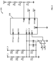
- FIG. 1 A multi-phase switched-mode power supply is illustrated in Fig. 1 , and indicated generally by reference number 100.
- the system 100 includes a pair of input terminals 102 and 104 for receiving an alternating current (AC) or direct current (DC) voltage input from an input power source V1, and a pair of output terminals Bulk+ and Bulk- for supplying a direct current (DC) voltage output to a load (not shown in Fig. 1 ).
- Fig. 1 illustrates an AC voltage input of 180V, other embodiments may receive DC voltage inputs, AC voltage inputs having lesser or greater voltages, etc.
- the power supply 100 includes a first phase circuit coupled between the pair of input terminals 102, 104 and the pair of output terminals Bulk+, Bulk-.
- the first phase circuit includes an inductor L1 coupled with a switch Q1.
- the power supply 100 also includes a second phase circuit interleaved with the first phase circuit between the pair of input terminals 102, 104 and the pair of output terminals Bulk+, Bulk-.
- the second phase circuit includes an inductor L2 coupled with a switch Q2.
- a control circuit 106 is configured to output a PWM signal DRV1 to the first switch Q1, and output a PWM signal DRV2 to the switch Q2.
- An on time of the PWM signal DRV2 is equal to an on time of the PWM signal DRV 1 plus a fixed offset time period.
- control circuit 106 is configured to determine a period between at least two rising edges of the PWM signal DRV1, determine an off trigger PWM signal according to the determined period, and change the PWM signal DRV2 to a logical low value when a falling edge of the off trigger PWM signal occurs while the PWM signal DRV2 has a logical high value.
- Fig. 2 illustrates an example wiring diagram of portions of the control circuit 106.
- a digital controller 208 includes a zero current detection input ZCD1 coupled with the inductor L1 to detect a zero current crossing at the inductor L1, and a zero current detection input ZCD2 coupled with the inductor L2 to detect a zero current crossing at the inductor L2.
- Fig. 1 illustrates a resistor R4 coupled between the inductor L1 and the digital controller 208 to generate the signal ZCD1, and a resistor R3 coupled between the inductor L2 and the digital controller 208 to generate the signal ZCD1.
- the digital controller 208 includes an AC line input AC_L and an AC neutral input AC_N. As shown in Figs. 1 and 2 , a voltage divider including the resistors R12, R10, R9 and R11 is coupled between the AC line input AC_L of the digital controller 208 and the line terminal 102 of the AC voltage input V1. A voltage divider including the resistors R16, R15, R13 and R14 is coupled between the AC neutral input AC_N of the digital controller 208 and the neutral terminal 104 of the AC voltage input V1. A diode D6 is coupled between the AC neutral input ACN of the digital controller 208 and a circuit ground, and a diode D7 is coupled between the AC line input AC_L of the digital controller 208 and the circuit ground.
- a current sense input CS of the digital controller is coupled to receive a signal from the amplifier X1, which amplifies the sensed differential current Csense+ and Csense- to determine a current through the current sense resistor Rsense shown in Fig. 1 .
- the controller 208 includes a feedback input FB for receiving the voltage output of the power supply 100.
- a voltage divider including the resistors R5, R6, R7 and R8 is coupled between the output terminal Bulk+ and the feedback input FB.
- the example resistor values illustrated in Figs. 1 and 2 are for purposes of illustration only, and other embodiments may use other suitable resistor values, may have more or less resistors, may have resistors coupled in other circuit arrangements, etc.
- the digital controller 208 also includes a control signal output DRVA for supplying the PWM signal DRV1 to the switch Q1, a control signal output DRVB for supplying the PWM signal DRV2 to the switch Q2, and a ground input coupled to the circuit ground.
- a control signal output DRVA for supplying the PWM signal DRV1 to the switch Q1
- a control signal output DRVB for supplying the PWM signal DRV2 to the switch Q2
- Fig. 3 illustrates a block diagram showing example components of the control circuit 106.
- the control circuit 106 includes a PWM generator circuit 310 to generate a pulse-width modulation (PWM) signal PWMA, and a PWM generator circuit 312 to generate the PWM signal PWMB.
- PWM pulse-width modulation
- the signal PWMA may define the signal DRV1 supplied to the switch Q1
- the signal PWMB may define the signal supplied to the switch Q2.
- the control circuit 106 includes a fixed offset circuit 314 coupled to and input of the PWM generator circuit 310 to add the fixed offset time period to the on time of the signal PWMB.
- the control circuit 106 includes a voltage error amplifier 316 coupled to compare the DC voltage output (BulkVolt) to a voltage reference (BulkVoltRef).
- the fixed offset circuit 314 is coupled to receive a combined signal (via the multiplier circuit 318) from an output of the voltage error amplifier 316 and an equivalent root mean square (RMS) voltage of the AC voltage input.
- the fixed offset time period may be a constant value which only requires one time trimming depending on the speed of phase adjustment.
- the fixed offset circuit 314 may include a hardware delay that replicates the function of adding additional on time via software.
- a frequency capture circuit 320 is coupled to determine the period between at least two rising edges of the signal PWMA.
- the frequency capture circuit 320 may include a digital timer or an analog voltage ramp for measuring an instantaneous voltage of the signal PWMA.
- the frequency capture circuit 320 may determine the period between at least two rising edges of the signal PWMA by measuring an average value of multiple cycles of the signal PWMA, by predicting a next cycle of the signal PWMA according to the voltage input, the voltage output and a latest duty cycle of the signal PWMA, etc.
- the control circuit 106 also includes an off trigger generator circuit 322 coupled between the frequency capture circuit 320 and the PWM generator circuit 312.
- the off trigger generator circuit 322 may be configured to generate an off trigger PWM signal with a 180 degree phase shift from the signal PWMA, by using one half of the determined period between the at least two rising edges of the signal PWMA, one half of the measured average value of the multiple cycles of the signal PWMA, one half of the predicted next cycle of the signal PWMA, etc.
- an on time of the off trigger PWM signal may be equal to the on time of the signal PWMA.
- the control circuit 106 includes a zero current detector (ZCD) circuit 324 coupled with the PWM generator circuit 310, for detecting a zero current crossing at the inductor L1.
- ZCD zero current detector
- a ZCD circuit 326 is coupled with the PWM generator circuit 312 to detect a zero current crossing at the inductor L2.
- Fig. 3 illustrates one particular arrangement of the components outside of the highlighted portion (e.g., the fixed offset circuit 314, the frequency capture circuit 320 and the off trigger generator circuit 322) of the control circuit 106 for performing example control methods described herein, in other embodiments the components may be arranged differently while the highlighted portion of the control circuit 106 performs example control methods described herein.
- Example control methods described herein may use zero current detection for each inductor L1 and L2 (e.g., each PFC choke), to allow the inductor to reset on its own.
- Each inductor L1 and L2 will reset at different times depending on the inductance, gate drive delay, instantaneous input voltage, and instantaneous output voltage. Due to the different reset timing, the switching frequency may be different for each phase.
- Some prior art control methods that only detect one phase and force the second phase to be out-of-phase at a certain phase angle depending of the number of phases may not allow the second phase to achieve valley switching or full reset, especially if the inductance is large (e.g., the power supply mostly operates at low frequency).
- Some prior art control methods that use ZCD detection for each inductor measure the frequency of both phases to keep them equal by adjusting the on time of one phase or both phases, and the control method sets the phase shift of the other phase(s).
- example control methods described herein may only measure the switching period of the main phase, and provide a fixed turn off point for the second phase (e.g., according to the on time and the period of the main phase).
- example control methods described herein may add a fixed additional on time for the other phases to allow the current reset point to shift to the right by operating at a lower frequency.
- the second phase is allowed to slowly shift on its own to a correct phase angle, until it reaches the turn off trigger point to fix the second phase in place.
- the on time is cut off due to the turn off trigger (e.g., from the off trigger generator circuit 322, etc.), which in reduces the switching period until both frequencies are the same (e.g., the switching frequency of each switch Q1 and Q2 is equal).
- the phase control may not require any complex calculation, such as implementing error calculation, etc.
- Each phase of the power supply 100 may adjust its phase on its own.
- Some prior art control methods use the rising or falling edge of a PWM signal, average across multiple cycles, and compare the average to a fixed reference to control the phase angle shift. This creates a higher processing requirement for the controller, especially for multi-phase operation where complex calculations are performed to provide the phase control for each individual phase.
- example control methods described herein may not require any complex calculations for multi-phase operation.
- a fixed turn off trigger is generated (e.g., based on the period of the main phase), and applied to each individual phase. Accordingly, each phase of the power supply may adjust its timing on its own, which reduces the hardware requirement for the controller.
- the power supply 100 optionally includes a power factor correction (PFC) circuit coupled between the pair of input terminals 102, 104 and the first and second phase circuits.
- the PFC circuit includes an electromagnetic interference (EMI) filter circuit 105.
- the EMI filter circuit 105 may include two inductors L3 and L4, two capacitors C3 and C4, more or less inductors, more or less capacitors, etc.
- the PFC circuit also includes a bridge circuit D 1 including four diodes.
- Fig. 1 illustrates the power supply 100 as including an AC voltage input and a PFC circuit with an EMI filter circuit 105 and a bridge circuit D1 for AC-DC power conversion
- other embodiments may include other suitable PFC circuits, other embodiments may be DC-DC converters that receive a DC voltage input, etc.
- the power supply 100 may use any suitable AC- DC or DC-DC converter topology, such as a buck converter topology, a boost converter topology, or a forward converter topology, etc.
- the power supply 100 may use variable frequency operations, interleaved operation, etc.
- the power supply 100 may include more than two interleaved phase circuits (e.g., three phases, four phases, etc.).
- Each phase circuit may include its own inductor and switch, and the control circuit 106 may generate PWM signals for each switch, with a separate off trigger PWM signal for each switch other than the switch of the first phase circuit.
- the power supply 100 may include an output capacitor C2 coupled between the pair of output terminals Bulk+ and Bulk-, a diode D3 coupled between the inductor L1 and the output terminal Bulk+, a diode D2 coupled between the inductor L2 and the output terminal Bulk+, and a capacitor C1 coupled with the inductors L1 and L2.
- the power supply 100 may include more or less capacitors and diodes, capacitors and diodes coupled in other arrangements, etc.
- the terminals 102, 104, Bulk+ and Bulk- may include any suitable electrical terminal, wire, circuit trace, etc., for receiving a voltage input from a voltage source or supplying a voltage output to a load.
- the control circuit 106 may be configured to control switching operation of the switches Q1 and Q2 to operate the power supply 100 in any suitable mode of operation, such as in a quasi-resonant mode of operation, a critically discontinuous mode of operation, etc.
- the control circuit 106 and the digital controller 208 may include any suitable microprocessor, microcontroller, integrated circuit, digital signal processor, etc., which may include memory.
- the control circuit 106 and the digital controller 208 may be configured to perform (e.g., operable to perform, etc.) any of the example processes described herein using any suitable hardware and/or software implementation.
- the control circuit 106 and the digital controller 208 may execute computer-executable instructions stored in a memory, may include one or more logic gates, control circuitry, etc., as described above.
- Fig. 4 illustrates example waveforms 400 showing the control signals PWMA and PWMB, and the inductor current A and inductor current B, during multiple switching cycles of the power supply 100.
- the control signal PWMA may be supplied to the switch Q1 of Fig. 1 and the control signal PWMB may be supplied to the switch Q2 of Fig. 1 .
- the inductor current A may represent a current through the inductor L1
- the inductor current B may represent a current through the inductor L2.
- the control signal PWMA has an on time Ton
- the control signal PWMB has an on time that is equal to Ton plus a fixed offset of additional on time.
- both of the control signals PWMA and PWMB go to a logical high value, and the inductor currents A and B ramp up.
- the control signal PWMB has a longer on time than the control signal PWMA due to the fixed offset
- the inductor current B ramps up to a higher value than the inductor current A before the control signal PWMB transitions to a logical low value.
- Fig. 4 illustrates adding additional on time to the control signal PWMB, in other embodiments the control method may be implemented by reducing the on time of the control signal PWMA.
- the inductor current A reaches a zero value, and the control signal PWMA goes to a logical high value again (e.g., due to the ZCD1 signal triggering the PWM generator 310 in Fig. 3 , etc.).
- the inductor current B is not yet zero at time T1, so the control signal PWMB does not go to a logical high value until time T2 (e.g., based on the ZCD2 signal triggering the PWM generator 312 when the inductor current B reaches zero at time T2, etc.).
- the delay between the rising edges of the control signals PWMA and PWMB is further increased at times T5 and T6.
- the offset value added to the control signal PWMB continually causes the inductor current B to ramp up higher than the inductor current A, and therefore extends the time for the inductor current B to reach relative to the inductor current A more and more each cycle.
- Fig. 5 illustrates example waveforms 500 showing how to determine the off trigger PWM signal based on the control signal PWMA, along with the inductor current A.
- periods between rising edges of the control signal PWMA are first determined.
- PERIOD3 identifies a time period between rising edges of the pulse Ton3 at time TO and the pulse Ton2 at time T2
- PERIOD2 identifies a period between rising edges of the pulse Ton2 at time T2 and the pulse Ton1 at time T4
- PERIOD 1 identifies a period between rising edges of the pulse Ton1 at time T4 and the pulse TonO at time T6.
- each pulse of the off trigger PWM signal starts at a 180 degree opposite phase of the pulses of the control signal PWMA.
- each pulse of the off trigger PWM signal may start halfway through the determined period between pulses of the control signal PWMA.
- Fig. 5 illustrates a rising edge of the pulse Ton3 of the off trigger PWM signal starting at time T1, which is the midpoint of the determined time period PERIOD3 between pulses of the control signal PWMA.
- the rising edge of the pulse Ton2 of the off trigger PWM signal occurs at T3, which is to the time T2 plus a delay of the prior time period PERIOD3 divided by two.
- the rising edge of the pulse Ton1 of the off trigger PWM signal occurs at T5, which is to the time T4 plus a delay of the prior time period PERIOD2 divided by two.
- the rising edge of the pulse TonO of the off trigger PWM signal occurs at T7, which is to the time T6 plus a delay of the prior time period PERIOD1 divided by two.
- the on time of each pulse of the off trigger PWM signal may be equal to the on time of each pulse of the control signal PWMA.
- Fig. 5 also illustrates falling edges of the pulses of the off trigger PWM signal, which may be used to turn off the control signal PWMB early as described further below.
- FIG. 6 illustrates example waveforms 600 showing the interaction of the off trigger PWM signal with the control signals PWMA and PWMB, and the inductor currents A and B. As shown in Fig. 6 , at time TO, pulses of both control signals PWMA and PWMB start at the same time.
- the control signal PWMB is at a logical low value at time T1, the control signal PWMB is not affected.
- the control signal PWMA goes to a logical high value in response to a zero current condition of the inductor current A, while the control signal PWMB does not go to a logical high value until time T3 (e.g., because the inductor current B does not reach a zero current condition until time T3 due to the offset added to the on time of the control signal PWMB, etc.).
- a falling edge of the off trigger PWM signal again occurs. Because the control signal PWMB is at a logical low value at time T4, the control signal PWMB is not affected.
- the control signal PWMA goes to a logical high value in response to a zero current condition of the inductor current A, while the control signal PWMB does not go to a logical high value until time T6 (e.g., because the inductor current B does not reach a zero current condition until time T6 due to the offset added to the on time of the control signal PWMB, etc.).
- a falling edge of the off trigger PWM signal occurs at time T7, while the control signal PWMB is at a logical high level. This causes the control signal PWMB to transition to a logical low level early, at the same time T7 as the falling edge of the off trigger PWM signal, instead of the control signal PWMB staying at the logical high value until its normal period of TonB (e.g., TonA plus an offset) has ended.
- TonB e.g., TonA plus an offset
- the shortened on time of the control signal PWMB at time T7 reduces the ramp up of the inductor current B, which leads to a steady state condition where the inductor currents A and B are equal and opposite phase to one another.
- the control signal PWMA goes to a logical high value
- both the off trigger PWM signal and the control signal PWMB go to logical high values.
- the falling edge of the off trigger PWM signal at time T10 cuts short the control signal PWMB again, to maintain the steady state operation of the inductor currents A and B.
- the offset value and the off trigger PWM signal allow the power supply 100 to start off with the control signals PWMA and PWMB starting at the same time, while continually adjusting the control signal PWMB over subsequent cycles according to the off trigger PWM signal, in order to reach and maintain a steady state operation of the inductor currents A and B as balanced and opposite phases to one another.
- the control signal PWMB may be again adjusted over subsequent cycles according to the off trigger PWM signal, in order to again reach and maintain a steady state operation of the inductor currents A and B as balanced and opposite phases to one another.
- an inductance of the inductor L 1 may be lower (or higher) than the inductance of the inductor L2.
- the switching frequency of the switches Q1 and Q2 may be the same.
- the switching frequency may be different where the second phase operates at a lower frequency. This may result in a similar function as illustrated in Fig. 6 , and adding the off trigger signal provides phase control for the different phases.
- the switching frequency may again be different where the second phase operates at a lower frequency.
- Peak current control may compare the sensed inductor current with the output of a compensator for PFC operation. This may result in a similar function as illustrated in Fig. 6 , and adding the off trigger signal provides phase control for the different phases.
- Fig. 7 illustrates example waveforms 700 showing currents and voltages of different components of the power supply 100 during four different load conditions. Specifically, Fig. 7 illustrates an AC voltage input VinAC, an input current lac, a current Ichoke1 through the inductor L1, a current Ichoke2 through the inductor L2, a voltage output Vbulk, and an output current lout.
- a first load condition is illustrated from zero to 200 milliseconds, at an output current of about two Amps.
- a second load condition is illustrated from 200 to 400 milliseconds at an output current of about four Amps, a third load condition is illustrated from 400 to 600 milliseconds at an output current of about 5.5 Amps, and a fourth load condition is illustrated from 600 to 800 milliseconds, at an output current of about 7.5 Amps.
- Fig. 8 illustrates example waveforms 800 showing currents and voltages of different components of the power supply 100 based on a 100% load condition for a one-half cycle of the AC voltage input. As shown in Fig. 8 , ripple cancellation is most effective when the current of the inductor L1 is 180 degrees out of phase with respect to the current though the inductor L2. Figs. 7 and 8 also illustrate the effectiveness of using the phase control techniques described herein for different stepped load conditions.
- Fig. 9 illustrates example waveforms 900 showing PWM control signals and inductor currents for a three phase power supply. For example, a control signal PWMA is supplied to a switch of a first phase circuit of the power supply, where the current A corresponds to a current through an inductor of the first phase circuit.
- a control signal PWMB is supplied to a switch of a second phase circuit of the power supply, where the current B corresponds to a current through an inductor of the second phase circuit.
- a control signal PWMC is supplied to a switch of a third phase circuit of the power supply, where the current C corresponds to a current through an inductor of the third phase circuit.
- a control signal DummyPWM has a frequency that is equal to double the frequency of a previous period of the control signal PWMA.
- the control signal DummyPWM has a duty cycle of ten percent.
- Each of the control signals PWMB and PWMC have an on time that is equal to an on time of the control signal PWMA plus a fixed offset.
- the off trigger for each phase PWMB and PWMC will have a different shift.
- the pseudo-code illustrated in Fig. 9 describes the off trigger for the signal PWMB as adding 33% of the previous period of the control signal PWMA to the start of a pulse of the control signal PWMA, and the off trigger for the signal PWMC as adding 66% of the previous period of the control signal PWMA to the start of a pulse of the control signal PWMA.
- the inductor currents A, B and C of the three phases reach a steady state balance after multiple cycles.
- the control signals PWMB and PWMC start out with a phase difference of ninety degrees relative to the control signal PWMA at time TO, although in other embodiments the control signals may all start at the same time, may start with different phase offsets, etc.
- a method controlling a multi- phase power supply includes a pair of input terminals for receiving an alternating current (AC) or direct current (DC) voltage input from an input power source, a pair of output terminals for supplying a direct current (DC) voltage output to a load, a first phase circuit coupled between the pair of input terminals and the pair of output terminals and including a first inductor coupled with a first switch, and a second phase circuit interleaved with the first phase circuit between the pair of input terminals and the pair of output terminals and including a second inductor coupled with a second switch.
- AC alternating current
- DC direct current
- the method includes outputting a first PWM signal to the first switch, and outputting a second PWM signal to the second switch.
- An on time of the second PWM signal is equal to an on time of the first PWM signal plus a fixed offset time period.
- the method also includes determining a period between at least two rising edges of the first PWM signal, determining an off trigger PWM signal according to the determined period, an changing the second PWM signal to a logical low value when a falling edge of the off trigger PWM signal occurs while the second PWM signal has a logical high value.
- Determining the period between the at least two rising edges of the first PWM signal may include measuring the period using a digital timer or an analog voltage ramp for measuring an instantaneous voltage of the first PWM signal.
- Generating the off trigger PWM signal may include generating the off trigger PWM signal with a 180 degree phase shift from the first PWM signal by using one half of the determined period between the two rising edges of the first PWM signal.
- determining the period between the at least two rising edges of the first PWM signal may include measuring an average value of multiple cycles of the first PWM signal or by predicting a next cycle of the first PWM signal according to the voltage input, the voltage output and a latest duty cycle of the first PWM signal.
- Generating the off trigger PWM signal may include generating the off trigger PWM signal with a 180 degree phase shift from the first PWM signal by using one half of the measured average value of the multiple cycles of the first PWM signal or one half of the predicted next cycle of the first PWM signal.
- An on time of the off trigger PWM signal is equal to the on time of the first PWM signal.
- the method may include initiating the first PWM signal and the second PWM signal at a same time during startup of the power supply, and continuing to change the second PWM signal until a switching period of first PWM signal is equal to a switching period of the second PWM signal.
- the method may include, in response to the switching periods of the first PWM signal and the second PWM signal being disturbed to become unequal, continuing to change the second PWM signal until the switching period of first PWM signal is again equal to the switching period of the second PWM signal.
- Example embodiments described herein may provide one or more (or none) of the following advantages: simplicity of control circuit design and phase control method, lower processing requirements for the phase control when implemented with more than two phases (e.g., a four phase converter, etc.), use of a cheaper controller, ease of implementation due to a lack of need for compensation for phase control (especially for more than two phase applications). For example, in a four-phase converter, each phase may require independent compensation that can affect the stability of the overall converter.
Landscapes
- Engineering & Computer Science (AREA)
- Power Engineering (AREA)
- Health & Medical Sciences (AREA)
- General Health & Medical Sciences (AREA)
- Physical Education & Sports Medicine (AREA)
- Primary Health Care (AREA)
- Epidemiology (AREA)
- Medical Informatics (AREA)
- Public Health (AREA)
- Biomedical Technology (AREA)
- Human Computer Interaction (AREA)
- Theoretical Computer Science (AREA)
- General Engineering & Computer Science (AREA)
- Biophysics (AREA)
- Life Sciences & Earth Sciences (AREA)
- Neurosurgery (AREA)
- Dermatology (AREA)
- Neurology (AREA)
- Multimedia (AREA)
- Physics & Mathematics (AREA)
- General Physics & Mathematics (AREA)
- General Business, Economics & Management (AREA)
- Business, Economics & Management (AREA)
- Dc-Dc Converters (AREA)
- Rectifiers (AREA)
- Stereo-Broadcasting Methods (AREA)
Claims (15)
- Mehrphasenschaltnetzteil (100), wobei das Netzteil (100) Folgendes umfasst:ein Paar Eingangsanschlüsse (102, 104) zum Empfangen eines Wechselstrom(AC)- oder Gleichstrom(DC)-Spannungseingangs von einer Eingangsleistungsquelle;ein Paar Ausgangsanschlüsse zum Zuführen eines Gleichstrom(DC)-Spannungsausgangs an einen Verbraucher;eine erste Phasenschaltung, die zwischen dem Paar Eingangsanschlüsse (102, 104) und dem Paar Ausgangsanschlüsse gekoppelt ist, wobei die erste Phasenschaltung einen ersten Induktor (L1) beinhaltet, der mit einem ersten Schalter (Q1) gekoppelt ist;eine zweite Phasenschaltung, die mit der ersten Phasenschaltung zwischen dem Paar Eingangsanschlüsse (102, 104) und dem Paar Ausgangsanschlüsse verschachtelt ist, wobei die zweite Phasenschaltung einen zweiten Induktor (L2) beinhaltet, der mit einem zweiten Schalter (Q2) gekoppelt ist; undeine Steuerschaltung (106), die zu Folgendem konfiguriert ist:Ausgeben eines ersten PWM-Signals an den ersten Schalter (Q1), wobei das erste PWM-Signal eine Vielzahl von Impulsen umfasst, wobei jeder Impuls bei einer Detektion eines Nulldurchgangs eines durch den ersten Induktor (L1) fließenden Stroms beginnt;Ausgeben eines zweiten PWM-Signals an den zweiten Schalter (Q2), wobei das zweite PWM-Signal eine Vielzahl von Impulsen umfasst, wobei jeder Impuls bei einer Detektion eines Nulldurchgangs eines durch den zweiten Induktor (L2) fließenden Stroms beginnt, wobei eine Einschaltdauer des zweiten PWM-Signals gleich einer Einschaltdauer des ersten PWM-Signals plus einer festen Versatzzeitperiode ist, um zu ermöglichen, dass sich der aktuelle Rücksetzpunkt der zweiten Phase über aufeinander folgende Zyklen langsam verschiebt;Bestimmen einer Periode zwischen zwei aufeinander folgenden ansteigenden Flanken des ersten PWM-Signals;Generieren eines Aus-Trigger-PWM-Signals zwischen aufeinander folgenden Impulsen des ersten PWM-Signals, sodass sich der Beginn eines Impulses des Aus-Trigger-PWM-Signals bei einer Phasenverschiebung, die basierend auf der zuvor bestimmten Periode bestimmt wird, vom Beginn eines Impulses des ersten PWM-Signals befindet; undÄndern des zweiten PWM-Signals auf einen logischen Low-Wert, wenn eine fallende Flanke des Aus-Trigger-PWM-Signals auftritt, während das zweite PWM-Signal einen logischen High-Wert aufweist.
- Netzteil (100) nach Anspruch 1, wobei:die Steuerschaltung (106) eine erste PWM-Generatorschaltung (310) beinhaltet, um das erste PWM-Signal zu generieren;die Steuerschaltung (106) eine zweite PWM-Generatorschaltung (312) beinhaltet, um das zweite PWM-Signal zu generieren; unddie Steuerschaltung (106) eine feste Versatzschaltung (314) beinhaltet, die an die zweite PWM-Generatorschaltung (312) gekoppelt ist und ein Eingang von dieser ist, um die feste Versatzzeitperiode zu der Einschaltzeit des zweiten PWM-Signals zu addieren.
- Netzteil (100) nach Anspruch 2, wobei die Steuerschaltung (106) einen Spannungsfehlerverstärker (316) beinhaltet, der gekoppelt ist, um den DC-Spannungsausgang mit einer Spannungsreferenz zu vergleichen, und die feste Versatzschaltung (314) gekoppelt ist, um ein kombiniertes Signal von einem Ausgang des Spannungsfehlerverstärkers (316) und eine äquivalente Effektivspannung (RMS-Spannung) des AC-Spannungseingangs zu empfangen.
- Netzteil (100) nach Anspruch 2 oder 3, wobei die Steuerschaltung (106) eine Frequenzerfassungsschaltung (320) beinhaltet, um die Periode zwischen den zwei aufeinander folgenden ansteigenden Flanken des ersten PWM-Signals zu bestimmen, und die Frequenzerfassungsschaltung (320) einen digitalen Zeitgeber oder eine analoge Spannungsrampe zum Messen einer momentanen Spannung des ersten PWM-Signals beinhaltet.
- Netzteil (100) nach Anspruch 4, wobei die Steuerschaltung (106) eine Aus-Trigger-Generatorschaltung (322) beinhaltet, die zwischen der Frequenzerfassungsschaltung (320) und der zweiten PWM-Generatorschaltung (312) gekoppelt ist, und die Aus-Trigger-Generatorschaltung (322) dazu konfiguriert ist, das Aus-Trigger-PWM-Signal mit einer Phasenverschiebung um 180 Grad von dem ersten PWM-Signal zu generieren, indem eine Hälfte der bestimmten Periode zwischen den zwei aufeinander folgenden ansteigenden Flanken des ersten PWM-Signals verwendet wird.
- Netzteil (100) nach Anspruch 4, wobei:die Frequenzerfassungsschaltung (320) dazu konfiguriert ist, die Periode zwischen den zwei aufeinander folgenden ansteigenden Flanken des ersten PWM-Signals durch Messen eines Mittelwerts mehrerer Zyklen des ersten PWM-Signals oder durch Vorhersagen eines nächsten Zyklus des ersten PWM-Signals gemäß dem Spannungseingang, dem Spannungsausgang und einem letzten Tastverhältnis des ersten PWM-Signals zu bestimmen;die Steuerschaltung (106) eine Aus-Trigger-Generatorschaltung (322) beinhaltet, die zwischen der Frequenzerfassungsschaltung (320) und der zweiten PWM-Generatorschaltung (312) gekoppelt ist; unddie Aus-Trigger-Generatorschaltung (322) dazu konfiguriert ist, das Aus-Trigger-PWM-Signal mit einer Phasenverschiebung um 180 Grad von dem ersten PWM-Signal zu generieren, indem eine Hälfte des gemessenen Mittelwerts der mehreren Zyklen des ersten PWM-Signals oder eine Hälfte des vorhergesagten nächsten Zyklus des ersten PWM-Signals verwendet wird.
- Netzteil (100) nach einem der Ansprüche 1-6, wobei eine Einschaltdauer des Aus-Trigger-PWM-Signals gleich der Einschaltdauer des ersten PWM-Signals ist.
- Netzteil (100) nach einem der Ansprüche 1-7, wobei die Steuerschaltung (106) eine erste Nullstromdetektorschaltung (ZCD-Schaltung) (324), die zwischen dem ersten Induktor (L1) und der ersten PWM-Generatorschaltung (310) gekoppelt ist, um einen Nullstromdurchgang an dem ersten Induktor (L1) zu detektieren, und eine zweite ZCD-Schaltung (326), die zwischen dem zweiten Induktor (L2) und der zweiten PWM-Generatorschaltung (312) gekoppelt ist, um einen Nullstromdurchgang an dem zweiten Induktor (L2) zu detektieren, beinhaltet.
- Netzteil (100) nach einem der Ansprüche 1-4, 7 und 8, ferner umfassend eine dritte Phasenschaltung, die mit der ersten Phasenschaltung und der zweiten Phasenschaltung zwischen dem Paar Eingangsanschlüsse (102, 104) und dem Paar Ausgangsanschlüsse verschachtelt ist, wobei die dritte Phasenschaltung einen dritten Induktor beinhaltet, der mit einem dritten Schalter gekoppelt ist.
- Netzteil (100) nach einem der Ansprüche 1-9, ferner umfassend eine Leistungsfaktorkorrekturschaltung (PFC-Schaltung), die zwischen dem Paar Eingangsanschlüsse (102, 104) und der ersten und der zweiten Phasenschaltung gekoppelt ist, wobei die PFC-Schaltung eine elektromagnetische Interferenz-Filterschaltung (EMI-Filterschaltung) (105), die mindestens zwei Kondensatoren (C3, C4) und mindestens zwei Induktoren (L3, L4) umfasst, und eine Brückenschaltung (D1), die mindestens vier Dioden umfasst, beinhaltet.
- Netzteil (100) nach einem der Ansprüche 1-10, ferner umfassend einen Ausgangskondensator (C2), der zwischen dem Paar Ausgangsanschlüsse gekoppelt ist, eine erste Diode (D3), die zwischen der ersten Phasenschaltung und einem ersten des Paares Ausgangsanschlüsse gekoppelt ist, und eine zweite Diode (D2), die zwischen der zweiten Phasenschaltung und dem ersten des Paares Ausgangsanschlüsse gekoppelt ist.
- Verfahren zum Steuern eines Mehrphasennetzteils (100), wobei das Netzteil (100) ein Paar Eingangsanschlüsse (102, 104) zum Empfangen eines Wechselstrom(AC)- oder Gleichstrom(DC)-Spannungseingangs von einer Eingangsleistungsquelle, ein Paar Ausgangsanschlüsse zum Zuführen eines Gleichstrom(DC)-Spannungsausgangs an einen Verbraucher, eine erste Phasenschaltung, die zwischen dem Paar Eingangsanschlüsse (102, 104) und dem Paar Ausgangsanschlüsse gekoppelt ist und einen ersten Induktor (L1), der mit einem ersten Schalter (Q1) gekoppelt ist, beinhaltet, und eine zweite Phasenschaltung beinhaltet, die mit der ersten Phasenschaltung zwischen dem Paar Eingangsanschlüsse (102, 104) und dem Paar Ausgangsanschlüsse verschachtelt ist und einen zweiten Induktor (L2), der mit einem zweiten Schalter (Q2) gekoppelt ist, beinhaltet, wobei das Verfahren Folgendes umfasst:Ausgeben eines ersten PWM-Signals an den ersten Schalter (Q1), wobei das erste PWM-Signal eine Vielzahl von Impulsen umfasst, wobei jeder Impuls bei einer Detektion eines Nulldurchgangs eines durch den ersten Induktor (L1) fließenden Stroms beginnt;Ausgeben eines zweiten PWM-Signals an den zweiten Schalter (Q2), wobei das zweite PWM-Signal eine Vielzahl von Impulsen umfasst, wobei jeder Impuls bei einer Detektion eines Nulldurchgangs eines durch den zweiten Induktor (L2) fließenden Stroms beginnt, wobei eine Einschaltdauer des zweiten PWM-Signals gleich einer Einschaltdauer des ersten PWM-Signals plus einer festen Versatzzeitperiode ist, um zu ermöglichen, dass sich der aktuelle Rücksetzpunkt der zweiten Phase über aufeinander folgende Zyklen langsam verschiebt;Bestimmen einer Periode zwischen zwei aufeinander folgenden ansteigenden Flanken des ersten PWM-Signals;Generieren eines Aus-Trigger-PWM-Signals zwischen aufeinander folgenden Impulsen des ersten PWM-Signals, sodass sich der Beginn eines Impulses des Aus-Trigger-PWM-Signals bei einer Phasenverschiebung, die basierend auf der zuvor bestimmten Periode bestimmt wird, vom Beginn eines Impulses des ersten PWM-Signals befindet; undÄndern des zweiten PWM-Signals auf einen logischen Low-Wert, wenn eine fallende Flanke des Aus-Trigger-PWM-Signals auftritt, während das zweite PWM-Signal einen logischen High-Wert aufweist.
- Verfahren nach Anspruch 12, wobei das Bestimmen der Periode zwischen den zwei aufeinander folgenden ansteigenden Flanken des ersten PWM-Signals Messen der Periode unter Verwendung eines digitalen Zeitgebers oder einer analogen Spannungsrampe zum Messen einer momentanen Spannung des ersten PWM-Signals beinhaltet.
- Verfahren nach Anspruch 13, wobei das Generieren des Aus-Trigger-PWM-Signals Generieren des Aus-Trigger-PWM-Signals mit einer Phasenverschiebung um 180 Grad von dem ersten PWM-Signal, indem eine Hälfte der bestimmten Periode zwischen den zwei ansteigenden Flanken des ersten PWM-Signals verwendet wird, beinhaltet.
- Verfahren nach Anspruch 13, wobei:das Bestimmen der Periode zwischen den zwei aufeinander folgenden ansteigenden Flanken des ersten PWM-Signals Messen eines Mittelwerts mehrerer Zyklen des ersten PWM-Signals oder durch Vorhersagen eines nächsten Zyklus des ersten PWM-Signals gemäß dem Spannungseingang, dem Spannungsausgang und einem letzten Tastverhältnis des ersten PWM-Signals beinhaltet; unddas Generieren des Aus-Trigger-PWM-Signals Generieren des Aus-Trigger-PWM-Signals mit einer Phasenverschiebung um 180 Grad von dem ersten PWM-Signal, indem eine Hälfte des gemessenen Mittelwerts der mehreren Zyklen des ersten PWM-Signals oder eine Hälfte des vorhergesagten nächsten Zyklus des ersten PWM-Signals verwendet wird, beinhaltet.
Applications Claiming Priority (1)
| Application Number | Priority Date | Filing Date | Title |
|---|---|---|---|
| US17/007,862 US11264908B1 (en) | 2020-08-31 | 2020-08-31 | Multi-phase switched-mode power supplies |
Publications (3)
| Publication Number | Publication Date |
|---|---|
| EP3961894A1 EP3961894A1 (de) | 2022-03-02 |
| EP3961894B1 true EP3961894B1 (de) | 2024-11-13 |
| EP3961894B8 EP3961894B8 (de) | 2024-12-18 |
Family
ID=77264938
Family Applications (1)
| Application Number | Title | Priority Date | Filing Date |
|---|---|---|---|
| EP21190243.2A Active EP3961894B8 (de) | 2020-08-31 | 2021-08-09 | Mehrphasenschaltnetzteile |
Country Status (6)
| Country | Link |
|---|---|
| US (2) | US11264908B1 (de) |
| EP (1) | EP3961894B8 (de) |
| JP (1) | JP7249388B2 (de) |
| CN (1) | CN114123818B (de) |
| PH (1) | PH12021050388A1 (de) |
| TW (1) | TWI784673B (de) |
Families Citing this family (7)
| Publication number | Priority date | Publication date | Assignee | Title |
|---|---|---|---|---|
| US11264908B1 (en) * | 2020-08-31 | 2022-03-01 | Astec International Limited | Multi-phase switched-mode power supplies |
| US11990267B2 (en) | 2020-09-23 | 2024-05-21 | Astec International Limited | Three-phase magnetics assembly |
| US11489438B2 (en) * | 2020-10-21 | 2022-11-01 | Astec International Limited | Inrush current limiting and surge protection circuit and system |
| CN115037143A (zh) * | 2022-07-06 | 2022-09-09 | 深圳市必易微电子股份有限公司 | 一种功率因素校正电路及其补偿方法 |
| JP2024064507A (ja) | 2022-10-28 | 2024-05-14 | 富士電機株式会社 | スイッチング制御回路、制御回路、電源回路 |
| US12401283B2 (en) * | 2023-02-03 | 2025-08-26 | L3Harris Technologies, Inc. | Method of mitigating saturation in interphase transformer of interleaved switched mode power supply during startup |
| US12438449B2 (en) * | 2023-05-16 | 2025-10-07 | Infineon Technologies Austria Ag | Power factor correction system, controller and method of controlling a power factor correction system |
Family Cites Families (23)
| Publication number | Priority date | Publication date | Assignee | Title |
|---|---|---|---|---|
| US5905369A (en) | 1996-10-17 | 1999-05-18 | Matsushita Electric Industrial Co., Ltd. | Variable frequency switching of synchronized interleaved switching converters |
| US6091233A (en) * | 1999-01-14 | 2000-07-18 | Micro Linear Corporation | Interleaved zero current switching in a power factor correction boost converter |
| US6987675B2 (en) * | 2003-05-23 | 2006-01-17 | Delta Electronics, Inc. | Soft-switched power converters |
| TW200507431A (en) | 2003-08-11 | 2005-02-16 | Delta Electronics Inc | Current-balancing method and device for controlling the power-factor-correction circuit interlacedly |
| US7701730B2 (en) | 2006-05-01 | 2010-04-20 | Texas Instruments Incorporated | Method and apparatus for power converters having phases spaced at desired phase angles |
| US7706151B2 (en) | 2006-05-01 | 2010-04-27 | Texas Instruments Incorporated | Method and apparatus for multi-phase power conversion |
| JP4850915B2 (ja) * | 2006-09-14 | 2012-01-11 | ルネサスエレクトロニクス株式会社 | Pfcコントローラ、スイッチングレギュレータ及び電源回路 |
| KR101410999B1 (ko) * | 2008-02-14 | 2014-06-24 | 페어차일드코리아반도체 주식회사 | 인터리브 스위칭 컨버터와 그의 제어 장치 및 방법 |
| JP4972142B2 (ja) * | 2009-10-26 | 2012-07-11 | 日立コンピュータ機器株式会社 | 力率改善装置及びその制御方法 |
| JP5391168B2 (ja) | 2010-09-03 | 2014-01-15 | 本田技研工業株式会社 | 複合型変圧器 |
| US8681519B2 (en) * | 2011-03-04 | 2014-03-25 | Astec International Limited | Variable input voltage PFC circuits, systems and power supplies with phase shifted power rails |
| US8842450B2 (en) * | 2011-04-12 | 2014-09-23 | Flextronics, Ap, Llc | Power converter using multiple phase-shifting quasi-resonant converters |
| TWI497886B (zh) * | 2013-05-10 | 2015-08-21 | Univ Nat Taiwan | 用於多相交錯直流電源轉換器的控制裝置及其控制方法 |
| CN104539155B (zh) * | 2014-12-09 | 2017-09-29 | 矽力杰半导体技术(杭州)有限公司 | 一种具有自均流的多相并联变换器及其控制方法 |
| US9722494B2 (en) * | 2015-04-30 | 2017-08-01 | Stmicroelectronics S.R.L. | Controller for multiphase boost converters |
| JP6559352B2 (ja) * | 2016-08-03 | 2019-08-14 | 三菱電機株式会社 | 電力変換装置、モータ駆動制御装置、送風機、圧縮機および空気調和機 |
| US10395819B2 (en) | 2016-08-30 | 2019-08-27 | Astec International Limited | Multiple phase power converters having integrated magnetic cores for transformer and inductor windings |
| US10044255B2 (en) * | 2016-10-27 | 2018-08-07 | Infineon Technologies Austria Ag | Multiphase power supply and phase control |
| EP3401935B1 (de) | 2017-05-08 | 2020-12-02 | Delta Electronics (Thailand) Public Co., Ltd. | Integriertes magnetisches bauteil und leistungswandler |
| US10491106B2 (en) * | 2017-08-09 | 2019-11-26 | Microchip Technology Incorporated | Digital control of switched boundary mode interleaved power converter |
| US10992230B1 (en) * | 2019-10-24 | 2021-04-27 | Wavious, Llc | Multi-phase switching mode power supply with adaptive synchronous drivers |
| US11108329B1 (en) * | 2020-02-28 | 2021-08-31 | Astec International Limited | Switch-mode power supplies including three-level LLC circuits for low line and high line operation |
| US11264908B1 (en) * | 2020-08-31 | 2022-03-01 | Astec International Limited | Multi-phase switched-mode power supplies |
-
2020
- 2020-08-31 US US17/007,862 patent/US11264908B1/en active Active
-
2021
- 2021-08-06 JP JP2021129657A patent/JP7249388B2/ja active Active
- 2021-08-09 EP EP21190243.2A patent/EP3961894B8/de active Active
- 2021-08-18 TW TW110130455A patent/TWI784673B/zh active
- 2021-08-20 PH PH1/2021/050388A patent/PH12021050388A1/en unknown
- 2021-08-31 CN CN202111015639.3A patent/CN114123818B/zh active Active
-
2022
- 2022-06-08 US US17/652,378 patent/US11779826B2/en active Active
Also Published As
| Publication number | Publication date |
|---|---|
| EP3961894A1 (de) | 2022-03-02 |
| JP7249388B2 (ja) | 2023-03-30 |
| CN114123818B (zh) | 2025-03-28 |
| US11264908B1 (en) | 2022-03-01 |
| US11779826B2 (en) | 2023-10-10 |
| TWI784673B (zh) | 2022-11-21 |
| US20220387872A1 (en) | 2022-12-08 |
| CN114123818A (zh) | 2022-03-01 |
| PH12021050388A1 (en) | 2023-01-09 |
| JP2022041912A (ja) | 2022-03-11 |
| TW202218303A (zh) | 2022-05-01 |
| EP3961894B8 (de) | 2024-12-18 |
| US20220069714A1 (en) | 2022-03-03 |
Similar Documents
| Publication | Publication Date | Title |
|---|---|---|
| EP3961894B1 (de) | Mehrphasenschaltnetzteile | |
| US7884588B2 (en) | Control method and device for a system of interleaved converters using a designated master converter | |
| US9537409B2 (en) | Method of feedback commanding a monophase resonant converter, a related monophase resonant converter and a polyphase resonant converter | |
| Jang et al. | Multiphase buck converters with extended duty cycle | |
| US6144194A (en) | Polyphase synchronous switching voltage regulators | |
| EP2355316B1 (de) | Verfahren und Vorrichtung zur Nulldurchgang-Bestimmung einer Wechselstrom-Eingangsspannung an einer Stromversorgung | |
| US7005835B2 (en) | Method and apparatus for load sharing in a multiphase switching power converter | |
| Huang | A new control for multi-phase buck converter with fast transient response | |
| US7109691B2 (en) | Systems for auto-interleaving synchronization in a multiphase switching power converter | |
| US6836103B2 (en) | Method and apparatus for dithering auto-synchronization of a multiphase switching power converter | |
| CN110731044A (zh) | 切换边界模式交错功率转换器的数字控制 | |
| US10008918B2 (en) | Phase-shifting optimization for asymmetric inductors in multi-phase DC-DC converters | |
| JP2005168106A (ja) | 電源装置 | |
| US11063520B2 (en) | Simplified hybrid PWM/PFM control method for SLLC converter | |
| JP2007135390A (ja) | 負荷ステップアップ過渡現象応答が改善された多相コンバータ | |
| JP4084194B2 (ja) | 非対称マルチコンバータ電源 | |
| US9250640B1 (en) | DC-to-DC converter controllers including oscillation prevention subsystems, and associated systems and methods | |
| JP5598247B2 (ja) | 電源装置 | |
| CN212323997U (zh) | 基于ucc28070实现超宽输入电压范围的外围电路 | |
| JP2003111396A (ja) | スイッチング電源 | |
| KR100831746B1 (ko) | 향상된 부하 계단 상승 과도응답을 갖는 다중위상 컨버터 | |
| Liu et al. | A Two-Phase Buck Converter With Ramped-Interleaved Digital Current Mode Constant On-Time Control | |
| JP2002369526A (ja) | スイッチング電源システム |
Legal Events
| Date | Code | Title | Description |
|---|---|---|---|
| PUAI | Public reference made under article 153(3) epc to a published international application that has entered the european phase |
Free format text: ORIGINAL CODE: 0009012 |
|
| STAA | Information on the status of an ep patent application or granted ep patent |
Free format text: STATUS: REQUEST FOR EXAMINATION WAS MADE |
|
| 17P | Request for examination filed |
Effective date: 20210809 |
|
| AK | Designated contracting states |
Kind code of ref document: A1 Designated state(s): AL AT BE BG CH CY CZ DE DK EE ES FI FR GB GR HR HU IE IS IT LI LT LU LV MC MK MT NL NO PL PT RO RS SE SI SK SM TR |
|
| RBV | Designated contracting states (corrected) |
Designated state(s): AL AT BE BG CH CY CZ DE DK EE ES FI FR GB GR HR HU IE IS IT LI LT LU LV MC MK MT NL NO PL PT RO RS SE SI SK SM TR |
|
| STAA | Information on the status of an ep patent application or granted ep patent |
Free format text: STATUS: EXAMINATION IS IN PROGRESS |
|
| 17Q | First examination report despatched |
Effective date: 20221212 |
|
| GRAP | Despatch of communication of intention to grant a patent |
Free format text: ORIGINAL CODE: EPIDOSNIGR1 |
|
| STAA | Information on the status of an ep patent application or granted ep patent |
Free format text: STATUS: GRANT OF PATENT IS INTENDED |
|
| RIC1 | Information provided on ipc code assigned before grant |
Ipc: G16H 40/67 20180101ALI20240513BHEP Ipc: G16H 20/30 20180101ALI20240513BHEP Ipc: H02M 1/36 20070101ALI20240513BHEP Ipc: H02M 3/158 20060101ALI20240513BHEP Ipc: H02M 1/42 20070101AFI20240513BHEP |
|
| INTG | Intention to grant announced |
Effective date: 20240606 |
|
| GRAS | Grant fee paid |
Free format text: ORIGINAL CODE: EPIDOSNIGR3 |
|
| GRAA | (expected) grant |
Free format text: ORIGINAL CODE: 0009210 |
|
| STAA | Information on the status of an ep patent application or granted ep patent |
Free format text: STATUS: THE PATENT HAS BEEN GRANTED |
|
| REG | Reference to a national code |
Ref country code: DE Ref legal event code: R108 Ref document number: 602021021710 Country of ref document: DE |
|
| AK | Designated contracting states |
Kind code of ref document: B1 Designated state(s): AL AT BE BG CH CY CZ DE DK EE ES FI FR GB GR HR HU IE IS IT LI LT LU LV MC MK MT NL NO PL PT RO RS SE SI SK SM TR |
|
| REG | Reference to a national code |
Ref country code: GB Ref legal event code: FG4D |
|
| REG | Reference to a national code |
Ref country code: CH Ref legal event code: EP |
|
| REG | Reference to a national code |
Ref country code: CH Ref legal event code: PK Free format text: BERICHTIGUNG B8 |
|
| RBV | Designated contracting states (corrected) |
Designated state(s): AL AT BE BG CH CY CZ DK EE ES FI FR GB GR HR HU IE IS IT LI LT LU LV MC MK MT NL NO PL PT RO RS SE SI SK SM TR |
|
| REG | Reference to a national code |
Ref country code: IE Ref legal event code: FG4D |
|
| REG | Reference to a national code |
Ref country code: DE Ref legal event code: R107 Ref document number: 602021021710 Country of ref document: DE |
|
| REG | Reference to a national code |
Ref country code: LT Ref legal event code: MG9D |
|
| REG | Reference to a national code |
Ref country code: NL Ref legal event code: MP Effective date: 20241113 |
|
| PG25 | Lapsed in a contracting state [announced via postgrant information from national office to epo] |
Ref country code: PT Free format text: LAPSE BECAUSE OF FAILURE TO SUBMIT A TRANSLATION OF THE DESCRIPTION OR TO PAY THE FEE WITHIN THE PRESCRIBED TIME-LIMIT Effective date: 20250313 Ref country code: HR Free format text: LAPSE BECAUSE OF FAILURE TO SUBMIT A TRANSLATION OF THE DESCRIPTION OR TO PAY THE FEE WITHIN THE PRESCRIBED TIME-LIMIT Effective date: 20241113 Ref country code: IS Free format text: LAPSE BECAUSE OF FAILURE TO SUBMIT A TRANSLATION OF THE DESCRIPTION OR TO PAY THE FEE WITHIN THE PRESCRIBED TIME-LIMIT Effective date: 20250313 |
|
| PG25 | Lapsed in a contracting state [announced via postgrant information from national office to epo] |
Ref country code: NL Free format text: LAPSE BECAUSE OF FAILURE TO SUBMIT A TRANSLATION OF THE DESCRIPTION OR TO PAY THE FEE WITHIN THE PRESCRIBED TIME-LIMIT Effective date: 20241113 Ref country code: FI Free format text: LAPSE BECAUSE OF FAILURE TO SUBMIT A TRANSLATION OF THE DESCRIPTION OR TO PAY THE FEE WITHIN THE PRESCRIBED TIME-LIMIT Effective date: 20241113 |
|
| REG | Reference to a national code |
Ref country code: AT Ref legal event code: MK05 Ref document number: 1742431 Country of ref document: AT Kind code of ref document: T Effective date: 20241113 |
|
| PG25 | Lapsed in a contracting state [announced via postgrant information from national office to epo] |
Ref country code: BG Free format text: LAPSE BECAUSE OF FAILURE TO SUBMIT A TRANSLATION OF THE DESCRIPTION OR TO PAY THE FEE WITHIN THE PRESCRIBED TIME-LIMIT Effective date: 20241113 |
|
| PG25 | Lapsed in a contracting state [announced via postgrant information from national office to epo] |
Ref country code: ES Free format text: LAPSE BECAUSE OF FAILURE TO SUBMIT A TRANSLATION OF THE DESCRIPTION OR TO PAY THE FEE WITHIN THE PRESCRIBED TIME-LIMIT Effective date: 20241113 |
|
| PG25 | Lapsed in a contracting state [announced via postgrant information from national office to epo] |
Ref country code: NO Free format text: LAPSE BECAUSE OF FAILURE TO SUBMIT A TRANSLATION OF THE DESCRIPTION OR TO PAY THE FEE WITHIN THE PRESCRIBED TIME-LIMIT Effective date: 20250213 |
|
| PG25 | Lapsed in a contracting state [announced via postgrant information from national office to epo] |
Ref country code: LV Free format text: LAPSE BECAUSE OF FAILURE TO SUBMIT A TRANSLATION OF THE DESCRIPTION OR TO PAY THE FEE WITHIN THE PRESCRIBED TIME-LIMIT Effective date: 20241113 Ref country code: AT Free format text: LAPSE BECAUSE OF FAILURE TO SUBMIT A TRANSLATION OF THE DESCRIPTION OR TO PAY THE FEE WITHIN THE PRESCRIBED TIME-LIMIT Effective date: 20241113 Ref country code: GR Free format text: LAPSE BECAUSE OF FAILURE TO SUBMIT A TRANSLATION OF THE DESCRIPTION OR TO PAY THE FEE WITHIN THE PRESCRIBED TIME-LIMIT Effective date: 20250214 |
|
| PG25 | Lapsed in a contracting state [announced via postgrant information from national office to epo] |
Ref country code: PL Free format text: LAPSE BECAUSE OF FAILURE TO SUBMIT A TRANSLATION OF THE DESCRIPTION OR TO PAY THE FEE WITHIN THE PRESCRIBED TIME-LIMIT Effective date: 20241113 |
|
| PG25 | Lapsed in a contracting state [announced via postgrant information from national office to epo] |
Ref country code: RS Free format text: LAPSE BECAUSE OF FAILURE TO SUBMIT A TRANSLATION OF THE DESCRIPTION OR TO PAY THE FEE WITHIN THE PRESCRIBED TIME-LIMIT Effective date: 20250213 |
|
| PG25 | Lapsed in a contracting state [announced via postgrant information from national office to epo] |
Ref country code: SM Free format text: LAPSE BECAUSE OF FAILURE TO SUBMIT A TRANSLATION OF THE DESCRIPTION OR TO PAY THE FEE WITHIN THE PRESCRIBED TIME-LIMIT Effective date: 20241113 |
|
| PG25 | Lapsed in a contracting state [announced via postgrant information from national office to epo] |
Ref country code: DK Free format text: LAPSE BECAUSE OF FAILURE TO SUBMIT A TRANSLATION OF THE DESCRIPTION OR TO PAY THE FEE WITHIN THE PRESCRIBED TIME-LIMIT Effective date: 20241113 |
|
| PG25 | Lapsed in a contracting state [announced via postgrant information from national office to epo] |
Ref country code: RO Free format text: LAPSE BECAUSE OF FAILURE TO SUBMIT A TRANSLATION OF THE DESCRIPTION OR TO PAY THE FEE WITHIN THE PRESCRIBED TIME-LIMIT Effective date: 20241113 |
|
| PG25 | Lapsed in a contracting state [announced via postgrant information from national office to epo] |
Ref country code: SK Free format text: LAPSE BECAUSE OF FAILURE TO SUBMIT A TRANSLATION OF THE DESCRIPTION OR TO PAY THE FEE WITHIN THE PRESCRIBED TIME-LIMIT Effective date: 20241113 |
|
| PG25 | Lapsed in a contracting state [announced via postgrant information from national office to epo] |
Ref country code: CZ Free format text: LAPSE BECAUSE OF FAILURE TO SUBMIT A TRANSLATION OF THE DESCRIPTION OR TO PAY THE FEE WITHIN THE PRESCRIBED TIME-LIMIT Effective date: 20241113 |
|
| PG25 | Lapsed in a contracting state [announced via postgrant information from national office to epo] |
Ref country code: IT Free format text: LAPSE BECAUSE OF FAILURE TO SUBMIT A TRANSLATION OF THE DESCRIPTION OR TO PAY THE FEE WITHIN THE PRESCRIBED TIME-LIMIT Effective date: 20241113 |
|
| PG25 | Lapsed in a contracting state [announced via postgrant information from national office to epo] |
Ref country code: SE Free format text: LAPSE BECAUSE OF FAILURE TO SUBMIT A TRANSLATION OF THE DESCRIPTION OR TO PAY THE FEE WITHIN THE PRESCRIBED TIME-LIMIT Effective date: 20241113 |
|
| PLBE | No opposition filed within time limit |
Free format text: ORIGINAL CODE: 0009261 |
|
| STAA | Information on the status of an ep patent application or granted ep patent |
Free format text: STATUS: NO OPPOSITION FILED WITHIN TIME LIMIT |
|
| 26N | No opposition filed |
Effective date: 20250814 |