EP3955304B1 - Integrated colour led micro-display - Google Patents
Integrated colour led micro-display Download PDFInfo
- Publication number
- EP3955304B1 EP3955304B1 EP21200332.1A EP21200332A EP3955304B1 EP 3955304 B1 EP3955304 B1 EP 3955304B1 EP 21200332 A EP21200332 A EP 21200332A EP 3955304 B1 EP3955304 B1 EP 3955304B1
- Authority
- EP
- European Patent Office
- Prior art keywords
- layer
- colour
- light
- gan
- micro
- Prior art date
- Legal status (The legal status is an assumption and is not a legal conclusion. Google has not performed a legal analysis and makes no representation as to the accuracy of the status listed.)
- Active
Links
- 239000010410 layer Substances 0.000 claims description 278
- 238000000034 method Methods 0.000 claims description 72
- 238000006243 chemical reaction Methods 0.000 claims description 64
- 239000000758 substrate Substances 0.000 claims description 54
- VYPSYNLAJGMNEJ-UHFFFAOYSA-N Silicium dioxide Chemical compound O=[Si]=O VYPSYNLAJGMNEJ-UHFFFAOYSA-N 0.000 claims description 50
- 229910052751 metal Inorganic materials 0.000 claims description 48
- 239000002184 metal Substances 0.000 claims description 48
- 230000008569 process Effects 0.000 claims description 40
- 238000005530 etching Methods 0.000 claims description 35
- 230000003287 optical effect Effects 0.000 claims description 29
- 238000000576 coating method Methods 0.000 claims description 28
- 239000011159 matrix material Substances 0.000 claims description 25
- 239000000377 silicon dioxide Substances 0.000 claims description 25
- 230000007480 spreading Effects 0.000 claims description 23
- 238000003892 spreading Methods 0.000 claims description 23
- XUIMIQQOPSSXEZ-UHFFFAOYSA-N Silicon Chemical compound [Si] XUIMIQQOPSSXEZ-UHFFFAOYSA-N 0.000 claims description 22
- 239000010703 silicon Substances 0.000 claims description 22
- 229910052710 silicon Inorganic materials 0.000 claims description 22
- 238000004519 manufacturing process Methods 0.000 claims description 21
- 235000012239 silicon dioxide Nutrition 0.000 claims description 21
- 239000011248 coating agent Substances 0.000 claims description 17
- 239000000463 material Substances 0.000 claims description 17
- 229910002601 GaN Inorganic materials 0.000 claims description 13
- 238000000605 extraction Methods 0.000 claims description 12
- 229910052594 sapphire Inorganic materials 0.000 claims description 11
- 239000010980 sapphire Substances 0.000 claims description 11
- 238000000151 deposition Methods 0.000 claims description 9
- 230000008021 deposition Effects 0.000 claims description 9
- 229910052697 platinum Inorganic materials 0.000 claims description 9
- 239000000126 substance Substances 0.000 claims description 9
- OAICVXFJPJFONN-UHFFFAOYSA-N Phosphorus Chemical compound [P] OAICVXFJPJFONN-UHFFFAOYSA-N 0.000 claims description 7
- 239000011521 glass Substances 0.000 claims description 7
- 229910052737 gold Inorganic materials 0.000 claims description 7
- 239000002096 quantum dot Substances 0.000 claims description 7
- 229910052681 coesite Inorganic materials 0.000 claims description 5
- 229910052906 cristobalite Inorganic materials 0.000 claims description 5
- HBMJWWWQQXIZIP-UHFFFAOYSA-N silicon carbide Chemical compound [Si+]#[C-] HBMJWWWQQXIZIP-UHFFFAOYSA-N 0.000 claims description 5
- 229910010271 silicon carbide Inorganic materials 0.000 claims description 5
- 230000003595 spectral effect Effects 0.000 claims description 5
- 229910052682 stishovite Inorganic materials 0.000 claims description 5
- 229910052905 tridymite Inorganic materials 0.000 claims description 5
- 230000000694 effects Effects 0.000 claims description 4
- 229910052709 silver Inorganic materials 0.000 claims description 4
- 229910052759 nickel Inorganic materials 0.000 claims description 3
- 229910052763 palladium Inorganic materials 0.000 claims description 3
- 238000009832 plasma treatment Methods 0.000 claims description 3
- 238000005086 pumping Methods 0.000 claims description 3
- 239000004020 conductor Substances 0.000 claims description 2
- 230000002708 enhancing effect Effects 0.000 claims description 2
- 229910000679 solder Inorganic materials 0.000 claims description 2
- 238000004064 recycling Methods 0.000 claims 1
- 239000002356 single layer Substances 0.000 claims 1
- 229920002120 photoresistant polymer Polymers 0.000 description 5
- 238000005498 polishing Methods 0.000 description 4
- 229920001296 polysiloxane Polymers 0.000 description 4
- 238000010561 standard procedure Methods 0.000 description 4
- 229920001621 AMOLED Polymers 0.000 description 3
- XPDWGBQVDMORPB-UHFFFAOYSA-N Fluoroform Chemical compound FC(F)F XPDWGBQVDMORPB-UHFFFAOYSA-N 0.000 description 3
- 238000000137 annealing Methods 0.000 description 3
- 230000015572 biosynthetic process Effects 0.000 description 3
- 230000000903 blocking effect Effects 0.000 description 3
- 238000001514 detection method Methods 0.000 description 3
- 238000005516 engineering process Methods 0.000 description 3
- 238000002955 isolation Methods 0.000 description 3
- 238000001020 plasma etching Methods 0.000 description 3
- 230000008901 benefit Effects 0.000 description 2
- 230000005540 biological transmission Effects 0.000 description 2
- 230000009849 deactivation Effects 0.000 description 2
- 230000000873 masking effect Effects 0.000 description 2
- 239000000203 mixture Substances 0.000 description 2
- 230000004048 modification Effects 0.000 description 2
- 238000012986 modification Methods 0.000 description 2
- 238000002161 passivation Methods 0.000 description 2
- 238000000059 patterning Methods 0.000 description 2
- 238000012805 post-processing Methods 0.000 description 2
- 229910052814 silicon oxide Inorganic materials 0.000 description 2
- 238000001039 wet etching Methods 0.000 description 2
- 239000004593 Epoxy Substances 0.000 description 1
- JMASRVWKEDWRBT-UHFFFAOYSA-N Gallium nitride Chemical group [Ga]#N JMASRVWKEDWRBT-UHFFFAOYSA-N 0.000 description 1
- ATJFFYVFTNAWJD-UHFFFAOYSA-N Tin Chemical compound [Sn] ATJFFYVFTNAWJD-UHFFFAOYSA-N 0.000 description 1
- 238000005411 Van der Waals force Methods 0.000 description 1
- 229910045601 alloy Inorganic materials 0.000 description 1
- 239000000956 alloy Substances 0.000 description 1
- 229910052782 aluminium Inorganic materials 0.000 description 1
- 238000003491 array Methods 0.000 description 1
- 239000002800 charge carrier Substances 0.000 description 1
- 238000007906 compression Methods 0.000 description 1
- 230000001010 compromised effect Effects 0.000 description 1
- 238000013461 design Methods 0.000 description 1
- 238000011161 development Methods 0.000 description 1
- 238000010586 diagram Methods 0.000 description 1
- 238000009826 distribution Methods 0.000 description 1
- 238000001312 dry etching Methods 0.000 description 1
- 238000011049 filling Methods 0.000 description 1
- 238000010438 heat treatment Methods 0.000 description 1
- 230000005525 hole transport Effects 0.000 description 1
- 229910052739 hydrogen Inorganic materials 0.000 description 1
- 239000001257 hydrogen Substances 0.000 description 1
- 229910052738 indium Inorganic materials 0.000 description 1
- APFVFJFRJDLVQX-UHFFFAOYSA-N indium atom Chemical compound [In] APFVFJFRJDLVQX-UHFFFAOYSA-N 0.000 description 1
- 238000002347 injection Methods 0.000 description 1
- 239000007924 injection Substances 0.000 description 1
- 239000004973 liquid crystal related substance Substances 0.000 description 1
- 230000003278 mimic effect Effects 0.000 description 1
- 229910003465 moissanite Inorganic materials 0.000 description 1
- 238000012544 monitoring process Methods 0.000 description 1
- 238000000623 plasma-assisted chemical vapour deposition Methods 0.000 description 1
- 238000007517 polishing process Methods 0.000 description 1
- 229920000642 polymer Polymers 0.000 description 1
- 238000002360 preparation method Methods 0.000 description 1
- 238000012545 processing Methods 0.000 description 1
- 238000003672 processing method Methods 0.000 description 1
- 238000002310 reflectometry Methods 0.000 description 1
- 239000011347 resin Substances 0.000 description 1
- 229920005989 resin Polymers 0.000 description 1
- 230000004044 response Effects 0.000 description 1
- 239000004065 semiconductor Substances 0.000 description 1
- 230000035945 sensitivity Effects 0.000 description 1
- 239000002904 solvent Substances 0.000 description 1
- 239000010409 thin film Substances 0.000 description 1
- 229910052718 tin Inorganic materials 0.000 description 1
- 230000000007 visual effect Effects 0.000 description 1
Images


Classifications
-
- H—ELECTRICITY
- H01—ELECTRIC ELEMENTS
- H01L—SEMICONDUCTOR DEVICES NOT COVERED BY CLASS H10
- H01L33/00—Semiconductor devices having potential barriers specially adapted for light emission; Processes or apparatus specially adapted for the manufacture or treatment thereof or of parts thereof; Details thereof
- H01L33/48—Semiconductor devices having potential barriers specially adapted for light emission; Processes or apparatus specially adapted for the manufacture or treatment thereof or of parts thereof; Details thereof characterised by the semiconductor body packages
- H01L33/50—Wavelength conversion elements
- H01L33/505—Wavelength conversion elements characterised by the shape, e.g. plate or foil
-
- H—ELECTRICITY
- H01—ELECTRIC ELEMENTS
- H01L—SEMICONDUCTOR DEVICES NOT COVERED BY CLASS H10
- H01L27/00—Devices consisting of a plurality of semiconductor or other solid-state components formed in or on a common substrate
- H01L27/15—Devices consisting of a plurality of semiconductor or other solid-state components formed in or on a common substrate including semiconductor components having potential barriers, specially adapted for light emission
- H01L27/153—Devices consisting of a plurality of semiconductor or other solid-state components formed in or on a common substrate including semiconductor components having potential barriers, specially adapted for light emission in a repetitive configuration, e.g. LED bars
- H01L27/156—Devices consisting of a plurality of semiconductor or other solid-state components formed in or on a common substrate including semiconductor components having potential barriers, specially adapted for light emission in a repetitive configuration, e.g. LED bars two-dimensional arrays
-
- H—ELECTRICITY
- H01—ELECTRIC ELEMENTS
- H01L—SEMICONDUCTOR DEVICES NOT COVERED BY CLASS H10
- H01L33/00—Semiconductor devices having potential barriers specially adapted for light emission; Processes or apparatus specially adapted for the manufacture or treatment thereof or of parts thereof; Details thereof
- H01L33/48—Semiconductor devices having potential barriers specially adapted for light emission; Processes or apparatus specially adapted for the manufacture or treatment thereof or of parts thereof; Details thereof characterised by the semiconductor body packages
- H01L33/50—Wavelength conversion elements
- H01L33/507—Wavelength conversion elements the elements being in intimate contact with parts other than the semiconductor body or integrated with parts other than the semiconductor body
-
- H—ELECTRICITY
- H01—ELECTRIC ELEMENTS
- H01L—SEMICONDUCTOR DEVICES NOT COVERED BY CLASS H10
- H01L25/00—Assemblies consisting of a plurality of individual semiconductor or other solid state devices ; Multistep manufacturing processes thereof
- H01L25/16—Assemblies consisting of a plurality of individual semiconductor or other solid state devices ; Multistep manufacturing processes thereof the devices being of types provided for in two or more different main groups of groups H01L27/00 - H01L33/00, or in a single subclass of H10K, H10N, e.g. forming hybrid circuits
- H01L25/167—Assemblies consisting of a plurality of individual semiconductor or other solid state devices ; Multistep manufacturing processes thereof the devices being of types provided for in two or more different main groups of groups H01L27/00 - H01L33/00, or in a single subclass of H10K, H10N, e.g. forming hybrid circuits comprising optoelectronic devices, e.g. LED, photodiodes
-
- H—ELECTRICITY
- H01—ELECTRIC ELEMENTS
- H01L—SEMICONDUCTOR DEVICES NOT COVERED BY CLASS H10
- H01L33/00—Semiconductor devices having potential barriers specially adapted for light emission; Processes or apparatus specially adapted for the manufacture or treatment thereof or of parts thereof; Details thereof
- H01L33/005—Processes
- H01L33/0093—Wafer bonding; Removal of the growth substrate
-
- H—ELECTRICITY
- H01—ELECTRIC ELEMENTS
- H01L—SEMICONDUCTOR DEVICES NOT COVERED BY CLASS H10
- H01L33/00—Semiconductor devices having potential barriers specially adapted for light emission; Processes or apparatus specially adapted for the manufacture or treatment thereof or of parts thereof; Details thereof
- H01L33/02—Semiconductor devices having potential barriers specially adapted for light emission; Processes or apparatus specially adapted for the manufacture or treatment thereof or of parts thereof; Details thereof characterised by the semiconductor bodies
- H01L33/20—Semiconductor devices having potential barriers specially adapted for light emission; Processes or apparatus specially adapted for the manufacture or treatment thereof or of parts thereof; Details thereof characterised by the semiconductor bodies with a particular shape, e.g. curved or truncated substrate
- H01L33/22—Roughened surfaces, e.g. at the interface between epitaxial layers
-
- H—ELECTRICITY
- H01—ELECTRIC ELEMENTS
- H01L—SEMICONDUCTOR DEVICES NOT COVERED BY CLASS H10
- H01L33/00—Semiconductor devices having potential barriers specially adapted for light emission; Processes or apparatus specially adapted for the manufacture or treatment thereof or of parts thereof; Details thereof
- H01L33/02—Semiconductor devices having potential barriers specially adapted for light emission; Processes or apparatus specially adapted for the manufacture or treatment thereof or of parts thereof; Details thereof characterised by the semiconductor bodies
- H01L33/26—Materials of the light emitting region
- H01L33/30—Materials of the light emitting region containing only elements of Group III and Group V of the Periodic Table
- H01L33/32—Materials of the light emitting region containing only elements of Group III and Group V of the Periodic Table containing nitrogen
-
- H—ELECTRICITY
- H01—ELECTRIC ELEMENTS
- H01L—SEMICONDUCTOR DEVICES NOT COVERED BY CLASS H10
- H01L33/00—Semiconductor devices having potential barriers specially adapted for light emission; Processes or apparatus specially adapted for the manufacture or treatment thereof or of parts thereof; Details thereof
- H01L33/48—Semiconductor devices having potential barriers specially adapted for light emission; Processes or apparatus specially adapted for the manufacture or treatment thereof or of parts thereof; Details thereof characterised by the semiconductor body packages
- H01L33/58—Optical field-shaping elements
- H01L33/60—Reflective elements
-
- H—ELECTRICITY
- H01—ELECTRIC ELEMENTS
- H01L—SEMICONDUCTOR DEVICES NOT COVERED BY CLASS H10
- H01L33/00—Semiconductor devices having potential barriers specially adapted for light emission; Processes or apparatus specially adapted for the manufacture or treatment thereof or of parts thereof; Details thereof
- H01L33/48—Semiconductor devices having potential barriers specially adapted for light emission; Processes or apparatus specially adapted for the manufacture or treatment thereof or of parts thereof; Details thereof characterised by the semiconductor body packages
- H01L33/62—Arrangements for conducting electric current to or from the semiconductor body, e.g. lead-frames, wire-bonds or solder balls
-
- H—ELECTRICITY
- H01—ELECTRIC ELEMENTS
- H01L—SEMICONDUCTOR DEVICES NOT COVERED BY CLASS H10
- H01L2924/00—Indexing scheme for arrangements or methods for connecting or disconnecting semiconductor or solid-state bodies as covered by H01L24/00
-
- H—ELECTRICITY
- H01—ELECTRIC ELEMENTS
- H01L—SEMICONDUCTOR DEVICES NOT COVERED BY CLASS H10
- H01L2924/00—Indexing scheme for arrangements or methods for connecting or disconnecting semiconductor or solid-state bodies as covered by H01L24/00
- H01L2924/0001—Technical content checked by a classifier
- H01L2924/0002—Not covered by any one of groups H01L24/00, H01L24/00 and H01L2224/00
-
- H—ELECTRICITY
- H01—ELECTRIC ELEMENTS
- H01L—SEMICONDUCTOR DEVICES NOT COVERED BY CLASS H10
- H01L2933/00—Details relating to devices covered by the group H01L33/00 but not provided for in its subgroups
- H01L2933/0008—Processes
- H01L2933/0033—Processes relating to semiconductor body packages
- H01L2933/0041—Processes relating to semiconductor body packages relating to wavelength conversion elements
-
- H—ELECTRICITY
- H01—ELECTRIC ELEMENTS
- H01L—SEMICONDUCTOR DEVICES NOT COVERED BY CLASS H10
- H01L2933/00—Details relating to devices covered by the group H01L33/00 but not provided for in its subgroups
- H01L2933/0008—Processes
- H01L2933/0033—Processes relating to semiconductor body packages
- H01L2933/0058—Processes relating to semiconductor body packages relating to optical field-shaping elements
-
- H—ELECTRICITY
- H01—ELECTRIC ELEMENTS
- H01L—SEMICONDUCTOR DEVICES NOT COVERED BY CLASS H10
- H01L2933/00—Details relating to devices covered by the group H01L33/00 but not provided for in its subgroups
- H01L2933/0008—Processes
- H01L2933/0033—Processes relating to semiconductor body packages
- H01L2933/0066—Processes relating to semiconductor body packages relating to arrangements for conducting electric current to or from the semiconductor body
-
- H—ELECTRICITY
- H01—ELECTRIC ELEMENTS
- H01L—SEMICONDUCTOR DEVICES NOT COVERED BY CLASS H10
- H01L2933/00—Details relating to devices covered by the group H01L33/00 but not provided for in its subgroups
- H01L2933/0091—Scattering means in or on the semiconductor body or semiconductor body package
-
- H—ELECTRICITY
- H01—ELECTRIC ELEMENTS
- H01L—SEMICONDUCTOR DEVICES NOT COVERED BY CLASS H10
- H01L33/00—Semiconductor devices having potential barriers specially adapted for light emission; Processes or apparatus specially adapted for the manufacture or treatment thereof or of parts thereof; Details thereof
- H01L33/44—Semiconductor devices having potential barriers specially adapted for light emission; Processes or apparatus specially adapted for the manufacture or treatment thereof or of parts thereof; Details thereof characterised by the coatings, e.g. passivation layer or anti-reflective coating
Definitions
- the present invention relates to a low power consumption high brightness display. More particularly, the present invention relates to an integrated colour light emitting diode (LED) micro-display and a method of manufacturing the integrated colour LED micro-display.
- LED light emitting diode
- OLED organic light emitting diode
- MEMS Liquid Crystal
- OLED organic light emitting diode
- the latter two are based on pattern generators located externally to a light source that is permanently on full brightness, and consequently require extra components to form the micro-display.
- a further basic drawback then relates to the power loss as all pixels must be addressed with light even if they are not used to display the image. The contrast ratio of such displays is also compromised.
- OLED technology is an emissive technology and in simple terms is based on an anode and cathode surrounding a fluorescent emitting layer. These techniques often use white light with colour filters for small pixel formation. Consequently, approximately 60 to 70% of the spectral range of the white pixels are lost/not needed to achieve the colour gamut in a RGB display.
- white OLEDs are in themselves less efficient than monochrome OLEDs, such that in the end only 10 to 20 % of the emitted light can actually be used. This does not take into account for the efficiencies of the overall OLED structure or how the light is extracted.
- the OLED structure is also more complex and involves electron transport layer, hole blocking layer and electron blocking layer all carefully controlled in thickness and refractive index. This is important for improved display performance as the electrically doped electron and hole transport layers enable enhanced charge injection and low operating voltages.
- the charge blocking layers help to confine charge carriers within the emission layer.
- other issues relate to the poor efficiencies and limited lifetimes in the blue OLED wavelength region and coupled with the low brightness levels mean that the display has fundamental limitations in performance.
- a GaN layer comprising p and n doped GaN regions and layers optimized for efficient light generation on top of which there is an ohmic current spreading layer and a layer of silicon dioxide.
- the ohmic current spreading layer may have a thickness of 20 nm.
- the layer of silicon dioxide may have a thickness of about 200 nm.
- the substrate layer may have a thickness of about 200 ⁇ m.
- the substrate layer may be any suitable material such as sapphire, silicon, GaN or silicon carbide.
- Example materials for the ohmic current spreading layer may be Ni/ Au or Ni/ Pt or Au/ Pt or Pt/ Ni/ Au Ni/ Ag or Pd or ITO or Ni/ ITO.
- the process may start with selective deactivation of p-GaN to form a pixel or an array of pixels. This can be described as follows:
- the process may start with a pixel or an array of pixel formation using physical etching of the p-GaN. This can be described as follows:
- the layer of silicon dioxide on the top of the pixels may then be removed and then re-deposited in the form of a complete layer of silicon dioxide.
- the complete layer of silicon dioxide may have a thickness of about 200 nm and may be deposited using any suitable technique such as PECVD.
- the area of the complete layer of silicon dioxide above the pixels may then be etched away to form windows to the ohmic current spreading layer and a window where the common contact is to be formed. In this embodiment this is the common n contact region.
- the silicon dioxide must be formed on the sidewall to provide passivation.
- the passivation of the sidewall is required when the n-contact region is etched locally.
- an n contact metal layer may be deposited in the area of the etch.
- the n contact metal may be Ti/ Au and may have a thickness of about 50/ 250 nm.
- the n contact metal layer may form a global contact and has an electrical function and/or functions as a guide for controlling a further etch step (an etch stop) in the manufacturing process.
- Bond pads may then be deposited to form n and p contacts.
- the bond pads may have a height of about 2 ⁇ m and a cross-section of about 8 ⁇ m x 8 ⁇ m. It is the intention to have the p and n bond pads of the same height.
- the bond pads can be formed on a masking layer such that the metal is deposited everywhere. This then this provide a means for chemical polishing of the device to provide a flat top layer with the metal and dielectric planar. Such a top structure then provides the means for uniform bonding (p and n bond pad stacks) at the same height.
- CMOS GaN to backplane control
- CMOS complementary metal-oxide-semiconductor
- NMOS complementary metal-oxide-semiconductor
- CMOS complementary metal-oxide-semiconductor
- TFT active Matrix OLED
- a temporary wafer made from Silicon may be bonded to the GaN wafer.
- the temporary wafer may have a thickness of about 500 ⁇ m and is significantly thicker than the GaN layer.
- the substrate layer may then be removed off with any suitable technique such as laser lift-off.
- any suitable technique such as laser lift-off.
- the substrate layer is silicon
- chemical mechanical polishing and etching or a combination of the techniques is possible. This has the added capability of forming micron features in the silicon substrate which can be used in the overall design.
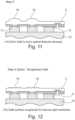
- the buffer or n-GaN layer may then be etched to form optical features which in the preferred embodiment may be in the form of micro-lenses.
- the optical features may be convex in shape to maximize emission and minimise optical crosstalk between pixels.
- the optical features may have a width of about 8 ⁇ m.
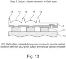
- the etching process may form roughened areas in proximity to the pixel.
- the roughened areas of 1 um in depth may be used to improve light extraction.
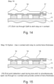
- GaN pillars may be formed.
- the GaN pillars may have a height of about 2 ⁇ m.
- the GaN pillars are also preferably truncated in shape to maximise optical isolation between LED pixel output to reduce optical crosstalk.
- the n-side etch process may be accurately controlled by etching to the n contact metal layer on the other side of the wafer to provide a suitable etch stop.
- etching By using real time plasma monitoring technique such as end point detection the etching depth can be accurately controlled in respect to the position of the GaN quantum well.
- the n contact layer may be used as an etch stop to control the lens thickness.
- the end point detection may be used during the lens etch to simultaneously open through to the n contact metal layer and provide control of the lens thickness.
- the conductive metal grid and/or opaque layer may reduce n-contact resistance hence and has a shielding effect.
- the metal grid and/or opaque layer may have a thickness of about 200nm and may be deposited using any suitable technique.
- an ITO conductive layer may be deposited instead of metal to create a transparent conductive layer.
- the selection of the appropriate ITO thickness may result in an anti-reflection coating to increase light transmission.
- GaN pillars may be coated with a layer of n metal to cover the sidewalls to minimize crosstalk.
- the layer of n metal may have a thickness of about 200 nm.
- the curved area of the optical features, or roughened areas may be covered with a dielectric coating.
- the dielectric coating may be made from silicon dioxide and may have a thickness of about 80 nm.
- the process also requires use of a colour converter which in some embodiments can have high reflectivity layers adjacent to sub-pixels to improve colour conversion efficiency and display contrast.
- the colour converter comprises a colour conversion layer, a substrate, a transparent layer and a mask.
- the colour conversion layer may be made from phosphor, quantum dot, organic substance or a combination thereof.
- the colour conversion layer may have a thickness of about 1 - 20 ⁇ m or preferably about 1 - 10 ⁇ m.
- the substrate may be made from glass, sapphire, silicon or any other suitable material. If blue light is used to optically pump the colour converter, not in accordance with the present invention, then it is not necessary to convert the incident light for the blue sub-pixel of the display.
- the mask is reflective and may be made from Au, Al or Ag.
- colour converter there may be a short pass filter which allows blue light to enter, but reflects longer converted light such as green and red.
- a colour converter which can be described as operating like a waveguide.
- a colour conversion layer transparent layer and a mask.
- a modified refractive index transparent layer which provides an optical waveguiding function and an un-modified refractive index layer.
- a colour converter which can be described as a long pass filter.
- the colour converter may have a long pass filter located below the colour conversion layer.
- the long pass filter may allow converted light to exit, but recycles blur unconverted light.
- the colour converter is brought up to and aligned with the LED layer.
- the colour converter may then be attached to the rest of the device.
- the colour converter may be pumped with blue light and there is a red/green colour conversion layer which is the phosphor layer.
- the layer may be a quantum dot or transparent/diffusing layer (blue) or a mixture thereof.
- the reflective mask has the ability to recirculate the light, minimises crosstalk and enhances display contrast.
- the reflective mask therefore has the ability to transmit blue light and reflect red and green light when a filter is placed before the transmittive layer. In an alternative, if the filter is placed after the transmittive layer then the blue light will be recirculate and the red and green transmitted.
- the temporary layer may be removed.
- the electronic drive layer may then be brought up to and aligned and attached to the metal bond pads on the LED.
- the bonding layer stack may include a low temperature solder material such as tin or indium, or alloys thereof.
- the planarity of the GaN p-layer also provides the capability to use low temperature direct bonding, including van der Waals forces, hydrogen bonds and strong covalent bonds.
- the electronic drive layer may be a CMOS, TFT or NMOS NMOS layer.
- the ability to use direct bonding techniques permits the ability to adapt thin film transistor techniques employed in matrix organic light emitting diode (AMOLED) micro-displays.
- AMOLED matrix organic light emitting diode
- the integrated colour LED micro-display may have a pixel layout implementation.
- three sub-pixels may be arranged in a 20 x 20 micron cell with the bond pads being positioned away from the pixels.
- the pixel layout implementation may comprise four sub-pixels included in each pixel with the bond pads positioned over the pixels.
- the present invention therefore resides in the provision of an integrated colour LED micro-display which provides a low power consumption high brightness display.
- the integrated colour LED micro-display may be formed as defined in the first aspect.
- the colour converter may comprise a colour conversion layer, a substrate, a transparent layer and a mask.
- the colour conversion layer may be made from phosphor, quantum dot, organic substance or a combination thereof.
- the colour conversion layer may have a thickness of about 5 - 20 ⁇ m or preferably about 10 - 12 ⁇ m.
- the substrate may be made from glass, sapphire, silicon or any other suitable material.
- the transparent layer may allow blue light to exit or alternatively may provide a diffusing or scattering function.
- the mask is reflective.
- the LED may comprise optical features which are in the form of lenses.
- the optical features may be convex in shape and maximize emission and minimise spectral crosstalk.
- the LED may also comprise a mask which may be opaque/black or reflective and may be made from metal such as Al or resin/polymer.
- the LED may also comprise bond pads which are deposited to form n and p contacts.
- the bond pads may have a height of about 2 ⁇ m and a cross-section of about 8 ⁇ m x 8 ⁇ m.
- the backplane control may comprise an electronic drive layer which has bond pads.
- the electronic drive layer may be a CMOS, TFT or NMOS NMOS layer.
- the bond pads on the backplane control are attached to bond pads on the LED.
- the present invention resides in the provision of a low power consumption high brightness display.
- Figures 1 to 41 show the process of making a micro-display according to the present invention. This is discussed below.
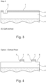
- Figure 1 shows a light emitting GaN layer 3 on top of which there is an ohmic current spreading layer 2 and a layer of silicon dioxide 1.
- the ohmic current spreading layer 2 has a thickness of about 20nm.
- the layer of silicon dioxide 1 has a thickness of about 200nm.
- the substrate layer 4 has a thickness of about 200um
- the substrate layer 4 can be any suitable material such as sapphire, silicon, GaN and silicon carbide.
- Example materials for the ohmic current spreading layer 2 are Ni/ Au or Ni/ Pt or Au/ Pt or Pt/ Ni/ Au Ni/ Ag or Pd or ITO or Ni/ ITO.
- Figure 2 represents an alternative process method where the GaN layer 3 has etched pixels comprising a layer of silicon dioxide 1 and ohmic current spreading layer 2. This is a standard technique to form the LED pixel.
- the spreading layer 2 is defined, typically to be the same size as the final pixel dimension.
- an etching process is performed on the device shown in Figure 1 which is a GaN modification process.
- the etching produces an etched area 5 where the GaN layer 3 is etched.
- the etching process is performed using any suitable etching process but is preferably performed by plasma etching using CF 3 but other techniques such as wet etching may be used. Etching down to the n material may be performed using plasma etching using Cl.
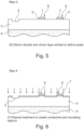
- a mask is then applied so as to enable pixel formation.
- There is a further etching process where the ohmic current spreading layer 2 and the layer of silicon dioxide 1 are etched away to form pixels 6.
- the etching process is performed using any suitable plasma etching process such as CHF 3 .
- the pixels 6 can be formed in a matrix pattern. This leaves pixels with dimensions of between 0.5 ⁇ m and 100 ⁇ m. A typical dimension is about 3 ⁇ m.
- a plasma treatment 7 which is used to create conductive and insulating regions.
- the unprotected GaN is exposed to a GaN modification process e.g. a plasma such as CHF 3 .
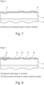
- the removal of the patterned feature may then be performed followed by annealing of the structure to form highly resistive layers in the areas exposed to plasma, whilst retaining conductive e.g. ohmic contact at the layers protected by the mask to form a pixel or an array of pixels.
- a mask layer is formed.
- the layer of silicon dioxide 1 on the top of the pixels 6 is removed and then re-deposited in the form of a complete layer 8 of a photoresist only or a dielectric e.g. SiO 2 with photoresist on top to pattern the SiO 2 layer.
- the mask is then opened above the n-contact area and the spreading material.
- a conductive contact is then deposited e.g. Ti:Au or other combinations. It should be apparent that the etch sidewall at the n-contact area has an electrical insulating layer on the sidewalls to prevent shorting across the p-n junction.
- the area of the complete layer 8 of silicon dioxide above the pixels 6 is etched away to form contact windows 10 to the ohmic current spreading layer 2 below to create contact.
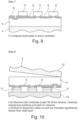
- an n contact metal layer 9 is deposited in the area of the etch 5.
- the n contact metal layer 9 forms a global contact and has an electrical function and/or functions as a guide for controlling a further etch step in the manufacturing process.
- bond pads 11 are deposited to form n and p contacts. This may use the same masking layer or alternatively a new mask.
- the p and n bond pad have the advantage of having the same height and thus improve the bonding probability of success for an array of LEDs.
- the n-pad etch depth can be used as both an accurate etch stop for the process later on i.e. when etching from the GaN side, exposed after laser lift off, and as a means to provide a connection for a distributed electrical contact on the backside of the wafer.
- the mask layer for forming the bond pad metal can provide a layer without topology and as such a process such as CMP - chemical mechanical polishing (damscene) can be used to planarise the metal to the top of the mask layer.
- This polishing process then enables the ability to have a flat bonding surface. Consequently, it will be possible to use a range of bonding processes including but not limited to flip-chip bump bonding (thermo-sonic or thermo-compression), or direct bonding or any other technique to form a mechanical and electrical bond to a backplane, e.g. CMOS, TFT or NMOS layer.
- the substrate layer 4 is removed off with any suitable technique such as laser lift-off.
- the substrate layer 4 can then undergo silicone, chemical mechanical polishing and etching for the silicone.
- the GaN on substrate (sapphire, etc.) is then bonded to a temporary wafer with the GaN surface in contact to this layer.
- Industry standard techniques may be used to detach the GaN layer from the substrate. In this particular example laser lift off is used.
- CMP can be used to remove silicon or GaN. This can then be combined with etching of the substrate so that features can be etched into the substrate.
- pillars can be left from the Si to provide isolation between sub-pixels.
- the temporary wafer 13 has a thickness which is significantly thicker than the GaN layer 3.
- the GaN layer is exposed on the backside a range of features can be formed in this structure. This can be to provide the means of extracting more light and/or providing features to reduce optical cross-talk between sub-pixels.
- the GaN layer 3 is etched to form optical features 14 which are in the form of lenses.
- the optical features 14 are convex in shape and maximize emission and minimise spectral crosstalk. It is also possible to deposit a layer on these features such as SiO 2 to act as an anti-reflection coating. In this particular feature, lenses are formed (the height can be accurately determined by using the etch stop) to increase light extraction and to reduce optical crosstalk between sub-pixels.
- the etching may be used to form roughened areas 15.
- the roughened areas 15 may be used to improve light extraction.
- a scattering surface is formed from etching.
- a layer or layers can be deposited to reduce the Fresnel reflections.
- Figure 13 is a further alternative where in the matrix etching process, GaN pillars 16 are formed.
- pillars 16 can therefore be formed between the light extraction features (in this example lenses). This can be formed in the GaN at the same time as the light extraction features using standard techniques.
- the pillars 16 can be formed in the original substrate (description in Figure 10 ) or they can be formed in the colour conversion substrate (described in Figure 23 ).
- the pillars 16 will ideally have smooth surfaces and a highly reflective structure, irrespective of the technique.
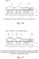
- the process as shown in Figure 14 then involves a further etching process where the GaN layer 3 is etched through to form an etched area 17 to the n contact metal layer 9 over the etched area 5.
- the light extraction feature (lens) and n opening can be simultaneously formed.
- the etching is performed by any suitable etching technique.
- Figure 15 shows an alternative where the n contact layer 9 is used as an etch stop to control the lens thickness.
- the end point detection is used during the lens etch 18 to simultaneously open through to the n contact metal layer 9 and provide control of the lens thickness.
- the preferred embodiment for the Figure 14 process is that the n-contact can be used as an etch stop so as to accurately control the etch depth of the lens and thus its proximity to the QW layers.
- Figure 16 shows that there is a deposition step where there is a deposition of conductive metal grid and/or opaque layer 19. This is similar to as described in Figure 9 and the described ability to form a distributed electrical contact on the exposed GaN face. In this instance this forms an electrical bridge between the bond pad and the conductive GaN face. In this instance an opaque conductor is used. Consequently, this is not deposited over the light extraction features.
- the conductive metal grid and/or opaque layer 40 reduces bias and has a shielding effect.
- Figure 17 represents an alternative where an ITO conductive layer 20 is deposited instead of metal to create a transparent conductive layer 20.
- the selection of the appropriate ITO thickness may result in an anti-reflection coating.
- a distributed n-contact can be formed.
- a transparent ITO layer can be deposited uniformly across the surface (can also be patterned so as not covering the light extraction feature). This can also be designed to have a thickness to reduce Fresnel reflections.
- Figure 18 is a further alternative where the GaN pillars 16 are coated with a layer 21 of n metal and may also cover the sidewalls to minimize crosstalk.
- This is a combination of Figures 10 and 17 where the metal can be patterned to provide distributed electrical contact and also provide reflective pillars.
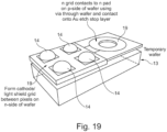
- Figure 19 is a schematic to illustrate the principle of forming light extraction features, an etch stop, distributed n contact and all bonded to a temporary carrier wafer such as silicon. This summarises the completed GaN chip which can then be integrated to a backplane control substrate and a colour converting substrate.
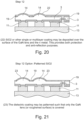
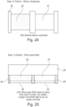
- a layer of SiOz or any other suitable type of single or multi-layer coating 22 may be deposited over the surface of the GaN lens 14 and the n metal layer 19. This provides both protection and an anti-reflection function.
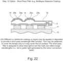
- coatings 24a, 24b may be deposited.
- the coatings 24a, 24b may be patterned to cover the optical features 14 only or it may cover the full surface.
- the short pass filter may be designed to allow blue light to exit the GaN but reflect longer wavelengths (i.e. the red or green light generated by the colour conversion layer).
- a short pass filter is employed. This efficiently transmits light in the pump wavelength region.
- each colour convertor provides a sub-pixel and is optically pumped (UV light).
- UV light In the case a blue pump wavelength is used, not in accordance with the present invention, the blue sub-pixel has no colour convertor substance but may have a material to mimic the colour convertor so that it has similar emission properties e.g.
- each LED pump is UV and there is a colour convertor for red, green and blue.
- a matrix is also formed between the sub-pixels for improved contrast and to prevent light leakage into the adjacent pixel. This may be a black matrix or a reflective structure.
- the matrix is formed on the colour conversion substrate.
- the colour converter comprises a colour conversion layer 25, a substrate 26, a transparent layer 27 and a mask 28.
- the substrate 26 may be made from glass, sapphire, silicon or any other suitable material.
- Figure 24 represents the option for forming the matrix for the colour converter region.
- the GaN on silicon substrate route it is possible to easily polish and etch the silicon substrate (for other substrates such as sapphire or SiC this is a much more difficult process). Consequently, it is possible to etch a matrix into the silicon using wet or dry etching capabilities. Using either etching technique can form matrices with high aspect ratio i.e. height to width of structure. The silicon will absorb light in the visible wavelength region, thus enhancing contrast. It is also possible to metallise the silicon matrix to provide reflection and enhance light conversion/ output.
- the colour converter comprises a colour conversion layer 25, a transparent layer 27 and an etched silicon area 29.
- Figure 25 is a further alternative colour converter.
- the short pass filter transmits light in blue and reflects at longer wavelengths i.e. green and red.
- a multi-layer coating can be formed on all cells. Consequently, the light converted, which is isotropic in nature, is reflected and will exit in the intended direction.
- the filter In the case of the blue emission pixel it may or may not be appropriate to have the filter. If pumping with UV light then the filter will be placed over all cells and have the properties of transmitting the UV pump but reflecting the longer wavelengths.
- Figure 26 is a further alternative colour converter which can be described as operating like a waveguide.
- a colour conversion layer 25 transparent layer 27 and a mask 28.
- a modified refractive index transparent layer 34 which provides an optical waveguiding function and an un-modified refractive index layer 35.
- the transparent layer 27 For the colour convertor transparent substrate (on which the colour convertors and matrix is formed), it is possible to modify the transparent layer 27. This can enable waveguides normal to the substrate plane to be formed. Consequently, the higher index layers will enhance optical waveguiding and enable the light to exit with a lower divergence.
- the index of the substrate can be modified as an example by laser induced effects to form the waveguide or can be formed by the etching and filling using higher index material. It is possible to use a transparent layer 34 of standard thickness of 0.5 to 2 mm. Furthermore, it is possible to use substrate layers 34 with thicknesses down to 20 ⁇ m.
- Figure 27 is a further alternative colour converter which can be described as a long pass filter.
- a further option/embodiment for the colour convertor transparent substrate is to also deposit a long pass filter, prior to the colour convertor being deposited on the substrate. This works in a similar fashion as Figure 24 except in this arrangement the unconverted blue light is reflected back to the colour conversion region.
- the colour convertor is patterned so as not to cover the blue sub-pixel.
- the colour converter has a long pass filter 31 located below the colour conversion layer 25.
- the long pass filter 31 allows converted light to exit, but recycles blue unconverted light.
- Figure 27 also shows that a long pass filter 32 would not be deposited over blue pixels to allow transmission of blue light.
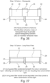
- a colour converter is brought up to and aligned with the LED layer.
- the colour conversion layer is therefore aligned to the LED substrate. This is in preparation for bonding of the two structures and is completed in such a manner that the GaN sub-pixel LEDs are aligned to the respective colour conversion region.
- the colour converter is attached to the rest of the device. Therefore, once suitable alignment has been completed the two layers are brought into contact and bonded together. As an example, this may be an epoxy type bonding process. It is also possible to perform this bond of the layer to provide a localised hermetic seal between the two substrates, thus providing enhanced protection to the colour conversion layer.
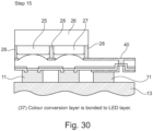
- the colour converter is pumped with blue light and there is a red/green colour conversion layer which is the phosphor layer.
- the layer is a quantum dot or transparent/diffusing layer (blue) or a mixture thereof.
- Figure 30 shows that extending vertically down from the glass substrate there is a reflective mask 28.
- the reflective mask 28 has the ability to recirculate the light, minimises crosstalk and enhances display contrast.
- the reflective mask 28 therefore has the ability to transmit blue light and reflect red and green light when a filter is placed before the layer. In an alternative, if the filter is placed after the layer then the blue light will be recirculate and the red and green transmitted.
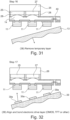
- the temporary layer 13 is removed from the combined layers. This may be achieved by heating, solvent and or any other standard technique.
- an electronic drive layer 39 is brought up to and aligned with the metal bond pads 11.
- the electronic drive layer 39 is a CMOS, TFT or NMOS layer.
- this is showing the bond stack with topology for clarity.
- the GaN modified LEDs can be used with a planarised surface. ( Figure 9 description is the way to provide a flat smooth surface). With no or little topology a range of different control backplanes can be bonded to the GaN surface including but not limited to CMOS, NMOS, TFT, etc.
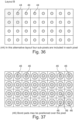
- Figure 34 is a plan view of pixel layout implementation in layout A.
- the three sub-pixels 43 are arranged in a 20 x 20 micron cell. This highlights the possible layout of the GaN led sub-pixels.
- three LEDs 43 are placed within the, as an example, 20 ⁇ m x 20 ⁇ m pixel region.
- the bond pads 39a are shown as being positioned away from the pixels 43.
- the bond pads associated with each LED sub-pixel are in general larger. This can distribute the bond force and reduce the likelihood of physical damage. Furthermore, the resistance can be reduced by increasing the bond pad dimensions.
- Using techniques such as GaN mod definition of the sub-pixel leads to improved performance as it reduces topology on the GaN surface and can provide LED sub-pixels with well-defined isolation layers.
- Figure 36 is a plan view of pixel layout implementation in layout B. In the embodiment shown there are four sub-pixels 44 included in each pixel. This is similar to Figure 34 but in this instance four GaN led sub-pixels 44 are defined within the 20 ⁇ m x 20 ⁇ m pixel region.
- the bond pads 46 may be positioned over the pixel 44. This is similar to Figure 35 with larger bond pads over each sub-pixel shown in Figure 36 .
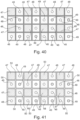
- FIG 39 there is shown an opaque/reflecting matrix 50. This is similar to Figure 38 also showing the matrix isolating each sub-pixel.
- Figure 41 there is a matrix of red colour conversion cells 47, green colour conversion cells 48, blue pixels without colour conversion cells 49 and an opaque/reflecting matrix 50. This is similar to Figure 40 and shows the matrix isolating each sub-pixel.
Landscapes
- Engineering & Computer Science (AREA)
- Microelectronics & Electronic Packaging (AREA)
- Power Engineering (AREA)
- Computer Hardware Design (AREA)
- Manufacturing & Machinery (AREA)
- Physics & Mathematics (AREA)
- Condensed Matter Physics & Semiconductors (AREA)
- General Physics & Mathematics (AREA)
- Led Devices (AREA)
- Devices For Indicating Variable Information By Combining Individual Elements (AREA)
Description
- The present invention relates to a low power consumption high brightness display. More particularly, the present invention relates to an integrated colour light emitting diode (LED) micro-display and a method of manufacturing the integrated colour LED micro-display.
- Although there are many colour micro-displays many of the prior art colour micro-displays have a number of disadvantages.
- There is extensive literature reporting the development of micro-displays using technologies such as organic light emitting diode (OLED), Liquid Crystal and MEMS. The latter two are based on pattern generators located externally to a light source that is permanently on full brightness, and consequently require extra components to form the micro-display. A further basic drawback then relates to the power loss as all pixels must be addressed with light even if they are not used to display the image. The contrast ratio of such displays is also compromised.
- OLED technology is an emissive technology and in simple terms is based on an anode and cathode surrounding a fluorescent emitting layer. These techniques often use white light with colour filters for small pixel formation. Consequently, approximately 60 to 70% of the spectral range of the white pixels are lost/not needed to achieve the colour gamut in a RGB display. In addition, white OLEDs are in themselves less efficient than monochrome OLEDs, such that in the end only 10 to 20 % of the emitted light can actually be used. This does not take into account for the efficiencies of the overall OLED structure or how the light is extracted.
- Moreover, the OLED structure is also more complex and involves electron transport layer, hole blocking layer and electron blocking layer all carefully controlled in thickness and refractive index. This is important for improved display performance as the electrically doped electron and hole transport layers enable enhanced charge injection and low operating voltages. The charge blocking layers help to confine charge carriers within the emission layer. Furthermore, other issues relate to the poor efficiencies and limited lifetimes in the blue OLED wavelength region and coupled with the low brightness levels mean that the display has fundamental limitations in performance.
- Techniques do exist to provide surface mount bonding of individual LEDs. Typically, pick and place techniques can only be used for large LEDs. Thus limiting the pixels per inch for a display. It also means that there is the need for two electrical contacts per pixel. For the former point, techniques have been developed to pick and place micro-LEDs. However, to provide electrical contacts presents challenges for small pixel pitch with post-processing required.
- Disadvantages of such systems can be summarised by the following:
- Manufacturing - time per flip-chip bond, simultaneous n and p connection for each pixel and ability to place pixels with < 10 µm dimensions;
- Post processing of pick and place micro-LEDs using semiconductor processing techniques. The provision of conformal contact layers across the LED arrays to form a secondary global contact. Or a combination of planarization techniques to provide a planarised structure on which a patterned contact layer is formed. The need to provide transparent contact layers for light escape or subsequent patterning of contact layers to enable this. The need to provide electrical connection to the control backplane.
- Performance - in particular selection of green LED devices with small chromatic variation over drive current and temperature. Requirement to have each green LED emission wavelength in a tight distribution due to the eye's sensitivity to small variations in wavelengths near the peak of its visual response (i.e. green) .
- It is an object of at least one aspect of the present invention to obviate or mitigate at least one or more of the aforementioned problems.
- It is a further object of at least one aspect of the present invention to provide a low power consumption high brightness integrated LED micro-display and a method of manufacturing said integrated LED micro-display.
-
US 2014/111408 A1 ,US 2012/223875 A1 ,US 2011/299044 A1 andWO 2014/030830 A1 disclose an integrated LED display. - According to a first aspect of the present invention there is provided a method of fabricating an integrated LED micro-display according to
claim 1. - The process of manufacturing involves a number of different stages which are set out below. It should also be apparent that in various embodiments, description is made with reference to figures. However, certain embodiments may be practiced without one or more of these specific details, or in combination with other known methods and configurations.
- First of all, there may be provided a GaN layer comprising p and n doped GaN regions and layers optimized for efficient light generation on top of which there is an ohmic current spreading layer and a layer of silicon dioxide. Located below the GaN layer there may be a substrate layer which is significantly thicker than the other layers. The ohmic current spreading layer may have a thickness of 20 nm. The layer of silicon dioxide may have a thickness of about 200 nm. The substrate layer may have a thickness of about 200 µm. The substrate layer may be any suitable material such as sapphire, silicon, GaN or silicon carbide. Example materials for the ohmic current spreading layer may be Ni/ Au or Ni/ Pt or Au/ Pt or Pt/ Ni/ Au Ni/ Ag or Pd or ITO or Ni/ ITO.
- The process may start with selective deactivation of p-GaN to form a pixel or an array of pixels. This can be described as follows:
- a first spreading layer is deposited on top of a GaN p layer e.g. Ni/ Au
- a patterned mask feature (e.g. photoresist) is then deposited on the spreading layer
- said structure is then exposed to a plasma such as Ar to remove the spreading followed by Cl2 to etch down ∼1um to the n-GaN (this process may be at a later stage in the process)
- a patterned mask feature (e.g. photoresist) is then deposited for pixel definition
- then exposing the layered structure to an etch (plasma or dry) to remove the first spreading layer from the areas not protected by the mask e.g. Ar
- said structure is then exposed to a plasma such as CHF3
- the removal of a patterned feature may then be performed
- then annealing of the structure to form highly resistive layers in the areas exposed to plasma, whilst retaining conductive e.g. ohmic contact at the layers protected by the mask to form a pixel or an array of pixels
- Alternatively, the process may start with a pixel or an array of pixel formation using physical etching of the p-GaN. This can can be described as follows:
- a first spreading layer is deposited on top of a GaN p layer e.g. Ni/ Au
- a patterned mask feature (e.g. photoresist) is then deposited on the spreading layer
- said structure is then exposed to a plasma such as Cl2 to etch down ∼1um to the n-GaN to leave pixels
- the removal of the patterned feature may then be performed
- then annealing of the structure to form conductive e.g. ohmic contact at the a pixel or an array of pixels
- The layer of silicon dioxide on the top of the pixels may then be removed and then re-deposited in the form of a complete layer of silicon dioxide. The complete layer of silicon dioxide may have a thickness of about 200 nm and may be deposited using any suitable technique such as PECVD.
- The area of the complete layer of silicon dioxide above the pixels may then be etched away to form windows to the ohmic current spreading layer and a window where the common contact is to be formed. In this embodiment this is the common n contact region. For the deactivation process the silicon dioxide must be formed on the sidewall to provide passivation. For the physical etched pixel or pixel array the passivation of the sidewall is required when the n-contact region is etched locally. In addition, an n contact metal layer may be deposited in the area of the etch. The n contact metal may be Ti/ Au and may have a thickness of about 50/ 250 nm. The n contact metal layer may form a global contact and has an electrical function and/or functions as a guide for controlling a further etch step (an etch stop) in the manufacturing process.
- Bond pads may then be deposited to form n and p contacts. The bond pads may have a height of about 2 µm and a cross-section of about 8 µm x 8 µm. It is the intention to have the p and n bond pads of the same height. Furthermore, the bond pads can be formed on a masking layer such that the metal is deposited everywhere. This then this provide a means for chemical polishing of the device to provide a flat top layer with the metal and dielectric planar. Such a top structure then provides the means for uniform bonding (p and n bond pad stacks) at the same height. Consequently, a range of bonding techniques can be utilized for GaN to backplane control (CMOS, TFT or NMOS layer) including but not limited to flip-chip bump bonding and direct bonding based on Van der Waal's forces. The latter is of particular interest as it permits bonding at low temperatures and with very little bond force. As the LED array size increases, the total bond force required becomes an important characteristic and can result in a physical limitation on array size. Also because of the low temperature bond, TFT backplane structures can be used which are similar in nature to Active Matrix OLED (AMOLED) control backplanes. This reduces the cost, complexity and provides a route to displays with larger physical dimensions.
- A temporary wafer made from Silicon may be bonded to the GaN wafer. The temporary wafer may have a thickness of about 500 µm and is significantly thicker than the GaN layer.
- The substrate layer may then be removed off with any suitable technique such as laser lift-off. In the event that the substrate layer is silicon, chemical mechanical polishing and etching or a combination of the techniques is possible. This has the added capability of forming micron features in the silicon substrate which can be used in the overall design.
- The buffer or n-GaN layer may then be etched to form optical features which in the preferred embodiment may be in the form of micro-lenses. The optical features may be convex in shape to maximize emission and minimise optical crosstalk between pixels. The optical features may have a width of about 8 µm.
- In an alternative, the etching process may form roughened areas in proximity to the pixel. The roughened areas of 1 um in depth may be used to improve light extraction.
- In a further alternative there may be a matrix etching process where GaN pillars may be formed. The GaN pillars may have a height of about 2 µm. The GaN pillars are also preferably truncated in shape to maximise optical isolation between LED pixel output to reduce optical crosstalk.
- The n-side etch process may be accurately controlled by etching to the n contact metal layer on the other side of the wafer to provide a suitable etch stop. By using real time plasma monitoring technique such as end point detection the etching depth can be accurately controlled in respect to the position of the GaN quantum well.
- In a further alternative the n contact layer may be used as an etch stop to control the lens thickness. The end point detection may be used during the lens etch to simultaneously open through to the n contact metal layer and provide control of the lens thickness.
- There may then be a deposition step where there may be a deposition of conductive metal grid and/or opaque layer. The conductive metal grid and/or opaque layer may reduce n-contact resistance hence and has a shielding effect. The metal grid and/or opaque layer may have a thickness of about 200nm and may be deposited using any suitable technique.
- In an alternative an ITO conductive layer may be deposited instead of metal to create a transparent conductive layer. The selection of the appropriate ITO thickness may result in an anti-reflection coating to increase light transmission.
- In a further alternative if GaN pillars are formed then they may be coated with a layer of n metal to cover the sidewalls to minimize crosstalk. The layer of n metal may have a thickness of about 200 nm.
- A layer of SiOz or any other suitable type of single or multi-layer coating may also be deposited over the surface of the GaN lens and the n metal layer. This provides both protection and an anti-reflection function of the GaN surface as it reduces Fresnel reflection. The coating may have a thickness of about 80 nm.
- In a further alternative only the curved area of the optical features, or roughened areas may be covered with a dielectric coating. The dielectric coating may be made from silicon dioxide and may have a thickness of about 80 nm.
- In a further alternative coatings may be deposited. There may therefore be multi-layer dielectric coatings. There may simply be one coating or additional coatings or layers which have the function of providing a short pass wavelength filter function. The coatings may be patterned to cover the optical features only or it may cover the full surface, The short pass filter may be designed to allow blue light to exit the GaN but reflect longer wavelengths (i.e. the red or green light generated by the colour conversion layer).
- The process also requires use of a colour converter which in some embodiments can have high reflectivity layers adjacent to sub-pixels to improve colour conversion efficiency and display contrast. The colour converter comprises a colour conversion layer, a substrate, a transparent layer and a mask. The colour conversion layer may be made from phosphor, quantum dot, organic substance or a combination thereof. The colour conversion layer may have a thickness of about 1 - 20 µm or preferably about 1 - 10 µm. The substrate may be made from glass, sapphire, silicon or any other suitable material. If blue light is used to optically pump the colour converter, not in accordance with the present invention, then it is not necessary to convert the incident light for the blue sub-pixel of the display. Consequently there may be no material in the blue cell or a transparent layer which may be made from silicone and allows blue light to exit or alternatively may provide a diffusing or scattering function to provide a similar beam profile as the red and green phosphors. The mask is reflective and may be made from Au, Al or Ag.
- In an alternative colour converter there may be an etched silicon substrate. The colour converter may comprises a colour conversion layer, a transparent layer and an etched silicon area.
- In an alternative colour converter there may be a short pass filter which allows blue light to enter, but reflects longer converted light such as green and red.
- In a further alternative there may be a colour converter which can be described as operating like a waveguide. As before there is a colour conversion layer, transparent layer and a mask. In addition there are opaque/reflective features, a modified refractive index transparent layer which provides an optical waveguiding function and an un-modified refractive index layer.
- In a further alternative there is a colour converter which can be described as a long pass filter. The colour converter may have a long pass filter located below the colour conversion layer. The long pass filter may allow converted light to exit, but recycles blur unconverted light.
- In the next step in the process the colour converter is brought up to and aligned with the LED layer.
- The colour converter may then be attached to the rest of the device. In an embodiment, not in accordance with the present invention, the colour converter may be pumped with blue light and there is a red/green colour conversion layer which is the phosphor layer. Alternatively, the layer may be a quantum dot or transparent/diffusing layer (blue) or a mixture thereof. Extending vertically down from the glass substrate there is a reflective mask. The reflective mask has the ability to recirculate the light, minimises crosstalk and enhances display contrast. The reflective mask therefore has the ability to transmit blue light and reflect red and green light when a filter is placed before the transmittive layer. In an alternative, if the filter is placed after the transmittive layer then the blue light will be recirculate and the red and green transmitted.
- In the next stage in the process the temporary layer may be removed.
- The electronic drive layer may then be brought up to and aligned and attached to the metal bond pads on the LED. The bonding layer stack may include a low temperature solder material such as tin or indium, or alloys thereof. The planarity of the GaN p-layer also provides the capability to use low temperature direct bonding, including van der Waals forces, hydrogen bonds and strong covalent bonds. The electronic drive layer may be a CMOS, TFT or NMOS NMOS layer. In particular, the ability to use direct bonding techniques permits the ability to adapt thin film transistor techniques employed in matrix organic light emitting diode (AMOLED) micro-displays.
- The integrated colour LED micro-display may have a pixel layout implementation. In one embodiment, three sub-pixels may be arranged in a 20 x 20 micron cell with the bond pads being positioned away from the pixels.
- In an alternative embodiment, the pixel layout implementation may comprise four sub-pixels included in each pixel with the bond pads positioned over the pixels.
- In an alternative integrated colour LED micro-display there may be an opaque/reflecting matrix.
- According to a second aspect of the present invention there is an integrated colour LED micro-display according to
claim 14. - Generally speaking, the present invention therefore resides in the provision of an integrated colour LED micro-display which provides a low power consumption high brightness display.
- The integrated colour LED micro-display may be formed as defined in the first aspect.
- The colour converter may comprise a colour conversion layer, a substrate, a transparent layer and a mask. The colour conversion layer may be made from phosphor, quantum dot, organic substance or a combination thereof. The colour conversion layer may have a thickness of about 5 - 20 µm or preferably about 10 - 12 µm. The substrate may be made from glass, sapphire, silicon or any other suitable material. The transparent layer may allow blue light to exit or alternatively may provide a diffusing or scattering function. The mask is reflective.
- The LED may comprise optical features which are in the form of lenses. The optical features may be convex in shape and maximize emission and minimise spectral crosstalk.
- The LED may also comprise a mask which may be opaque/black or reflective and may be made from metal such as Al or resin/polymer.
- The LED may also comprise bond pads which are deposited to form n and p contacts. The bond pads may have a height of about 2 µm and a cross-section of about 8 µm x 8 µm.
- The backplane control may comprise an electronic drive layer which has bond pads. The electronic drive layer may be a CMOS, TFT or NMOS NMOS layer.
- The bond pads on the backplane control are attached to bond pads on the LED.
- Embodiments of the present invention will now be described, by way of example only, with reference to the accompanying drawings in which:
-
Figure 1 represents a GaN layer on top of which there is an ohmic current spreading layer and a layer of silicon dioxide and below there is a sapphire substrate layer according to an embodiment of the present invention; -
Figure 2 represents an alternative processing method where a GaN layer has etched pixels comprising a layer of silicon dioxide and ohmic current spreading layer according to an embodiment of the present invention; -
Figure 3 represents an etching process performed on the device shown inFigure 1 according to an embodiment of the present invention; -
Figure 4 represents an alternative device to that shown inFigure 2 which is etched in the GaN layer around pixels to form an etched area according to an embodiment of the present invention; -
Figure 5 represents a further etching process where the ohmic current spreading layer and the layer of silicon dioxide are etched away to form pixels according to an embodiment of the present invention; -
Figure 6 represents a plasma treatment which is used to create conductive and insulating regions according to an embodiment of the present invention; -
Figure 7 represents the layer of silicon dioxide on the top of the pixels being removed and then re-deposited in the form of a complete layer of silicon dioxide according to an embodiment of the present invention; -
Figure 8 represents the area of the complete layer of silicon dioxide above the pixels being etched away to form contact windows according to an embodiment of the present invention; -
Figure 9 represents bond pads deposited to form n and p contacts according to an embodiment of the present invention; -
Figure 10 represents the substrate layer being removed according to an embodiment of the present invention; -
Figure 11 represents the GaN layer being etched to form optical features according to an embodiment of the present invention; -
Figure 12 represents an alternative etching method to form roughened areas according to an embodiment of the present invention; -
Figure 13 represents a further alternative to the etching method where the matrix etching process forms GaN pillars according to an embodiment of the present invention; -
Figure 14 represents a further alternative to the etching method where the GaN layer is etched through to form an etch to an n contact metal layer according to an embodiment of the present invention; -
Figure 15 represents a further alternative where the n contact layer is used as an etch stop to control the lens thickness according to an embodiment of the present invention; -
Figure 16 represents a deposition step where there is a deposition of conductive metal grid and/or opaque layer according to an embodiment of the present invention; -
Figure 17 represents an alternative deposition step where an ITO conductive layer is deposited instead of metal to create a transparent conductive layer according to an embodiment of the present invention; -
Figure 18 represents a further alternative where GaN pillars are coated with a layer of n metal according to an embodiment of the present invention; -
Figure 19 is an upper perspective view of the device shown inFigure 16 according to an embodiment of the present invention; -
Figure 20 represents the process where a layer of SiO2 or any other suitable type of single or multi-layer coating is deposited over the surface of the GaN lens and the n metal layer according to an embodiment of the present invention; -
Figure 21 represents a further alternative where only the curved area of the optical features are covered with a dielectric coating according to an embodiment of the present invention; -
Figure 22 represents is a further alternative where coatings are deposited to have the function of providing a short pass wavelength filter function according to an embodiment of the present invention; -
Figure 23 represents a colour converter according to an embodiment of the present invention; -
Figure 24 represents an alternative colour converter where there is an etched silicon substrate according to an embodiment of the present invention; -
Figure 25 represents a further alternative colour converter which is a short pass filter according to an embodiment of the present invention; -
Figure 26 represents a further alternative colour converter which can be described as operating like a waveguide according to an embodiment of the present invention; -
Figure 27 represents a further alternative colour converter which can be described as a long pass filter according to an embodiment of the present invention -
Figure 28 represents the colour converter being brought up to and aligned with an LED layer according to an embodiment of the present invention; -
Figure 29 , represents a further view of the colour conversion layer being aligned above the rest of the LED layer; -
Figure 30 represents a colour converter attached to the rest of the device according to an embodiment of the present invention; -
Figure 31 represents a temporary layer being removed according to an embodiment of the present invention; -
Figure 32 represents an electronic drive layer being brought up to and aligned with metal bond pads according to an embodiment of the present invention; -
Figure 33 represents metal bond pads being attached to the bond pads according to an embodiment of the present invention; -
Figures 34 and 35 represent a plan view of pixel layout implementation according to an embodiment of the present invention; -
Figure 36 and 37 represents a plan view of a further pixel layout implementation according to an embodiment of the present invention; -
Figure 38 represents a red colour conversion cell, a green colour conversion layer and a blue pixel without colour conversion cell according to an embodiment not forming part of the present invention; -
Figure 39 represents a colour conversion cell where there is an opaque/reflecting matrix according to an embodiment of the present invention; -
Figure 40 represents a matrix of red colour conversion cells, green colour conversion cells and blue pixels without colour conversion cells according to an embodiment not forming part of the present invention; and -
Figure 41 represents a matrix of red colour conversion cells, green colour conversion cells, blue pixels without colour conversion cells and an opaque/reflecting matrix according to an embodiment not forming part of the present invention; - Generally speaking, the present invention resides in the provision of a low power consumption high brightness display.
-
Figures 1 to 41 show the process of making a micro-display according to the present invention. This is discussed below. -
Figure 1 shows a light emittingGaN layer 3 on top of which there is an ohmic current spreadinglayer 2 and a layer ofsilicon dioxide 1. Located below theGaN layer 3 there is asubstrate layer 4 which is significantly thicker than the other layers. The ohmic current spreadinglayer 2 has a thickness of about 20nm. The layer ofsilicon dioxide 1 has a thickness of about 200nm. Thesubstrate layer 4 has a thickness of about 200um Thesubstrate layer 4 can be any suitable material such as sapphire, silicon, GaN and silicon carbide. Example materials for the ohmic current spreadinglayer 2 are Ni/ Au or Ni/ Pt or Au/ Pt or Pt/ Ni/ Au Ni/ Ag or Pd or ITO or Ni/ ITO. -
Figure 2 represents an alternative process method where theGaN layer 3 has etched pixels comprising a layer ofsilicon dioxide 1 and ohmic current spreadinglayer 2. This is a standard technique to form the LED pixel. InFigure 2 the spreadinglayer 2 is defined, typically to be the same size as the final pixel dimension. - In
Figure 3 an etching process is performed on the device shown inFigure 1 which is a GaN modification process. The etching produces an etchedarea 5 where theGaN layer 3 is etched. The etching process is performed using any suitable etching process but is preferably performed by plasma etching using CF3 but other techniques such as wet etching may be used. Etching down to the n material may be performed using plasma etching using Cl. - In
Figure 4 the alternative device shown inFigure 2 is etched in theGaN layer 3 around the pixels to form an etchedarea 5. - As show in
Figure 5 a mask is then applied so as to enable pixel formation. There is a further etching process where the ohmic current spreadinglayer 2 and the layer ofsilicon dioxide 1 are etched away to formpixels 6. The etching process is performed using any suitable plasma etching process such as CHF3. Thepixels 6 can be formed in a matrix pattern. This leaves pixels with dimensions of between 0.5 µm and 100 µm. A typical dimension is about 3µm. - In the process step shown in
Figure 6 , there is aplasma treatment 7 which is used to create conductive and insulating regions. The unprotected GaN is exposed to a GaN modification process e.g. a plasma such as CHF3. The removal of the patterned feature may then be performed followed by annealing of the structure to form highly resistive layers in the areas exposed to plasma, whilst retaining conductive e.g. ohmic contact at the layers protected by the mask to form a pixel or an array of pixels. - In
Figure 7 a mask layer is formed. The layer ofsilicon dioxide 1 on the top of thepixels 6 is removed and then re-deposited in the form of acomplete layer 8 of a photoresist only or a dielectric e.g. SiO2 with photoresist on top to pattern the SiO2 layer. - In
Figure 8 , the mask is then opened above the n-contact area and the spreading material. A conductive contact is then deposited e.g. Ti:Au or other combinations. It should be apparent that the etch sidewall at the n-contact area has an electrical insulating layer on the sidewalls to prevent shorting across the p-n junction. The area of thecomplete layer 8 of silicon dioxide above thepixels 6 is etched away to formcontact windows 10 to the ohmic current spreadinglayer 2 below to create contact. In addition, an ncontact metal layer 9 is deposited in the area of theetch 5. The ncontact metal layer 9 forms a global contact and has an electrical function and/or functions as a guide for controlling a further etch step in the manufacturing process. - In
Figure 9 ,bond pads 11 are deposited to form n and p contacts. This may use the same masking layer or alternatively a new mask. The p and n bond pad have the advantage of having the same height and thus improve the bonding probability of success for an array of LEDs. The n-pad etch depth can be used as both an accurate etch stop for the process later on i.e. when etching from the GaN side, exposed after laser lift off, and as a means to provide a connection for a distributed electrical contact on the backside of the wafer. Furthermore, the mask layer for forming the bond pad metal can provide a layer without topology and as such a process such as CMP - chemical mechanical polishing (damscene) can be used to planarise the metal to the top of the mask layer. This polishing process then enables the ability to have a flat bonding surface. Consequently, it will be possible to use a range of bonding processes including but not limited to flip-chip bump bonding (thermo-sonic or thermo-compression), or direct bonding or any other technique to form a mechanical and electrical bond to a backplane, e.g. CMOS, TFT or NMOS layer. - As shown in
Figure 10 , thesubstrate layer 4 is removed off with any suitable technique such as laser lift-off. Thesubstrate layer 4 can then undergo silicone, chemical mechanical polishing and etching for the silicone. The GaN on substrate (sapphire, etc.) is then bonded to a temporary wafer with the GaN surface in contact to this layer. Industry standard techniques may be used to detach the GaN layer from the substrate. In this particular example laser lift off is used. Alternatively, CMP can be used to remove silicon or GaN. This can then be combined with etching of the substrate so that features can be etched into the substrate. As is shown later (Figure 13 ) pillars can be left from the Si to provide isolation between sub-pixels. Thetemporary wafer 13 has a thickness which is significantly thicker than theGaN layer 3. - In
Figure 11 , now that the GaN layer is exposed on the backside a range of features can be formed in this structure. This can be to provide the means of extracting more light and/or providing features to reduce optical cross-talk between sub-pixels. TheGaN layer 3 is etched to formoptical features 14 which are in the form of lenses. The optical features 14 are convex in shape and maximize emission and minimise spectral crosstalk. It is also possible to deposit a layer on these features such as SiO2 to act as an anti-reflection coating. In this particular feature, lenses are formed (the height can be accurately determined by using the etch stop) to increase light extraction and to reduce optical crosstalk between sub-pixels. - As shown in
Figure 12 , in an alternative the etching may be used to form roughenedareas 15. The roughenedareas 15 may be used to improve light extraction. In this case a scattering surface is formed from etching. LikeFigure 11 a layer or layers can be deposited to reduce the Fresnel reflections. -
Figure 13 is a further alternative where in the matrix etching process,GaN pillars 16 are formed. As described inFigure 10 ,pillars 16 can therefore be formed between the light extraction features (in this example lenses). This can be formed in the GaN at the same time as the light extraction features using standard techniques. Alternatively, thepillars 16 can be formed in the original substrate (description inFigure 10 ) or they can be formed in the colour conversion substrate (described inFigure 23 ). Thepillars 16 will ideally have smooth surfaces and a highly reflective structure, irrespective of the technique. - The process as shown in
Figure 14 then involves a further etching process where theGaN layer 3 is etched through to form an etchedarea 17 to the ncontact metal layer 9 over the etchedarea 5. In this particular instance the light extraction feature (lens) and n opening can be simultaneously formed. The etching is performed by any suitable etching technique. -
Figure 15 shows an alternative where then contact layer 9 is used as an etch stop to control the lens thickness. The end point detection is used during thelens etch 18 to simultaneously open through to the ncontact metal layer 9 and provide control of the lens thickness. As described inFigure 9 , the preferred embodiment for theFigure 14 process is that the n-contact can be used as an etch stop so as to accurately control the etch depth of the lens and thus its proximity to the QW layers. -
Figure 16 then shows that there is a deposition step where there is a deposition of conductive metal grid and/oropaque layer 19. This is similar to as described inFigure 9 and the described ability to form a distributed electrical contact on the exposed GaN face.
In this instance this forms an electrical bridge between the bond pad and the conductive GaN face. In this instance an opaque conductor is used. Consequently, this is not deposited over the light extraction features. The conductive metal grid and/oropaque layer 40 reduces bias and has a shielding effect. -
Figure 17 represents an alternative where an ITOconductive layer 20 is deposited instead of metal to create a transparentconductive layer 20. The selection of the appropriate ITO thickness may result in an anti-reflection coating. LikeFigure 16 a distributed n-contact can be formed. However, in this instance a transparent ITO layer can be deposited uniformly across the surface (can also be patterned so as not covering the light extraction feature). This can also be designed to have a thickness to reduce Fresnel reflections. -
Figure 18 is a further alternative where theGaN pillars 16 are coated with alayer 21 of n metal and may also cover the sidewalls to minimize crosstalk. This is a combination ofFigures 10 and17 where the metal can be patterned to provide distributed electrical contact and also provide reflective pillars. -
Figure 19 is a schematic to illustrate the principle of forming light extraction features, an etch stop, distributed n contact and all bonded to a temporary carrier wafer such as silicon. This summarises the completed GaN chip which can then be integrated to a backplane control substrate and a colour converting substrate. - In
Figure 20 a layer of SiOz or any other suitable type of single ormulti-layer coating 22 may be deposited over the surface of theGaN lens 14 and then metal layer 19. This provides both protection and an anti-reflection function. - In
Figure 21 there is a further alternative where only the curved area of the optical features 14 (or roughened areas 15) are covered with adielectric coating 23. Patterning is therefore only used to deposit over the light extraction area. - In
Figure 22 there is a further alternative wherecoatings coatings optical features 14 only or it may cover the full surface. The short pass filter may be designed to allow blue light to exit the GaN but reflect longer wavelengths (i.e. the red or green light generated by the colour conversion layer). LikeFigure 20 and 21 one of the great advantages of present technique is that many different layers can be deposited over the light extraction area. In this particular arrangement a short pass filter is employed. This efficiently transmits light in the pump wavelength region. - It then reflects longer wavelengths i.e. green and red so that the converted light which gets back to the GaN surface has a higher probability of exiting in the direction of the end-user.
- In
Figure 23 shows that now that the GaN layer has been prepared the next stage is to form a colour convertor region. The preferred route is to use a separate substrate as this provides enhanced flexibility, although colour convertors could be placed on the GaN surface. In this case the colour convertor may be a phosphor, quantum dot, organic substance or a combination. The colour convertor substrate can be a range of materials such as glass, sapphire, silicone, etc. In this instance each colour convertor provides a sub-pixel and is optically pumped (UV light). In the case a blue pump wavelength is used, not in accordance with the present invention, the blue sub-pixel has no colour convertor substance but may have a material to mimic the colour convertor so that it has similar emission properties e.g. beam divergence In accordance with the present invention, each LED pump is UV and there is a colour convertor for red, green and blue. A matrix is also formed between the sub-pixels for improved contrast and to prevent light leakage into the adjacent pixel. This may be a black matrix or a reflective structure. Typically the matrix is formed on the colour conversion substrate. The colour converter comprises acolour conversion layer 25, asubstrate 26, atransparent layer 27 and amask 28. Thesubstrate 26 may be made from glass, sapphire, silicon or any other suitable material. -
Figure 24 represents the option for forming the matrix for the colour converter region. In the event that the GaN on silicon substrate route is used, it is possible to easily polish and etch the silicon substrate (for other substrates such as sapphire or SiC this is a much more difficult process). Consequently, it is possible to etch a matrix into the silicon using wet or dry etching capabilities. Using either etching technique can form matrices with high aspect ratio i.e. height to width of structure. The silicon will absorb light in the visible wavelength region, thus enhancing contrast. It is also possible to metallise the silicon matrix to provide reflection and enhance light conversion/ output. The colour converter comprises acolour conversion layer 25, atransparent layer 27 and an etchedsilicon area 29. -
Figure 25 is a further alternative colour converter. To enhance performance it is possible to include a filter on the colour convertor layer. The short pass filter transmits light in blue and reflects at longer wavelengths i.e. green and red. For simplicity a multi-layer coating can be formed on all cells. Consequently, the light converted, which is isotropic in nature, is reflected and will exit in the intended direction. In the case of the blue emission pixel it may or may not be appropriate to have the filter. If pumping with UV light then the filter will be placed over all cells and have the properties of transmitting the UV pump but reflecting the longer wavelengths. -
Figure 26 is a further alternative colour converter which can be described as operating like a waveguide. As before there is acolour conversion layer 25,transparent layer 27 and amask 28. In addition there are opaque/reflective features 33, a modified refractive indextransparent layer 34 which provides an optical waveguiding function and an un-modifiedrefractive index layer 35. For the colour convertor transparent substrate (on which the colour convertors and matrix is formed), it is possible to modify thetransparent layer 27. This can enable waveguides normal to the substrate plane to be formed. Consequently, the higher index layers will enhance optical waveguiding and enable the light to exit with a lower divergence. The index of the substrate can be modified as an example by laser induced effects to form the waveguide or can be formed by the etching and filling using higher index material. It is possible to use atransparent layer 34 of standard thickness of 0.5 to 2 mm. Furthermore, it is possible to usesubstrate layers 34 with thicknesses down to 20 µm. -
Figure 27 is a further alternative colour converter which can be described as a long pass filter. A further option/embodiment for the colour convertor transparent substrate is to also deposit a long pass filter, prior to the colour convertor being deposited on the substrate. This works in a similar fashion asFigure 24 except in this arrangement the unconverted blue light is reflected back to the colour conversion region. The colour convertor is patterned so as not to cover the blue sub-pixel. The colour converter has along pass filter 31 located below thecolour conversion layer 25. Thelong pass filter 31 allows converted light to exit, but recycles blue unconverted light.Figure 27 also shows that along pass filter 32 would not be deposited over blue pixels to allow transmission of blue light. - In the next step shown in
Figure 28 , a colour converter is brought up to and aligned with the LED layer. In this diagram the colour conversion layer is therefore aligned to the LED substrate. This is in preparation for bonding of the two structures and is completed in such a manner that the GaN sub-pixel LEDs are aligned to the respective colour conversion region. - In
Figure 29 , there is a further view of the colour conversion layer being aligned above the rest of the LED layer. This is a schematic ofFigure 28 . This highlights the transparent substrate for the colour conversion layer and the temporary wafer used to support the thin GaN LED layer. - In
Figure 30 , the colour converter is attached to the rest of the device. Therefore, once suitable alignment has been completed the two layers are brought into contact and bonded together. As an example, this may be an epoxy type bonding process. It is also possible to perform this bond of the layer to provide a localised hermetic seal between the two substrates, thus providing enhanced protection to the colour conversion layer. In an embodiment not forming part of the present invention, the colour converter is pumped with blue light and there is a red/green colour conversion layer which is the phosphor layer. Alternatively, the layer is a quantum dot or transparent/diffusing layer (blue) or a mixture thereof.Figure 30 shows that extending vertically down from the glass substrate there is areflective mask 28.
Thereflective mask 28 has the ability to recirculate the light, minimises crosstalk and enhances display contrast. Thereflective mask 28 therefore has the ability to transmit blue light and reflect red and green light when a filter is placed before the layer. In an alternative, if the filter is placed after the layer then the blue light will be recirculate and the red and green transmitted. - In
Figure 31 , thetemporary layer 13 is removed from the combined layers. This may be achieved by heating, solvent and or any other standard technique. - In
Figure 32 , anelectronic drive layer 39 is brought up to and aligned with themetal bond pads 11. Theelectronic drive layer 39 is a CMOS, TFT or NMOS layer. In the Figure this is showing the bond stack with topology for clarity. In the preferred embodiment the GaN modified LEDs can be used with a planarised surface. (Figure 9 description is the way to provide a flat smooth surface). With no or little topology a range of different control backplanes can be bonded to the GaN surface including but not limited to CMOS, NMOS, TFT, etc. - In
Figure 33 themetal bond pads 39a are attached to thebond pads 11. This is the completed micro-display structure highlighting many of the features necessary to provide display capability. -
Figure 34 is a plan view of pixel layout implementation in layout A. In the embodiment shown the three sub-pixels 43 are arranged in a 20 x 20 micron cell. This highlights the possible layout of the GaN led sub-pixels. In this particular configuration, threeLEDs 43 are placed within the, as an example, 20 µm x 20 µm pixel region. - In
Figure 35 thebond pads 39a are shown as being positioned away from thepixels 43. The bond pads associated with each LED sub-pixel are in general larger. This can distribute the bond force and reduce the likelihood of physical damage. Furthermore, the resistance can be reduced by increasing the bond pad dimensions. Using techniques such as GaN mod definition of the sub-pixel leads to improved performance as it reduces topology on the GaN surface and can provide LED sub-pixels with well-defined isolation layers. -
Figure 36 is a plan view of pixel layout implementation in layout B. In the embodiment shown there are four sub-pixels 44 included in each pixel. This is similar toFigure 34 but in this instance four GaN led sub-pixels 44 are defined within the 20 µm x 20 µm pixel region. - In
Figure 37 thebond pads 46 may be positioned over thepixel 44. This is similar toFigure 35 with larger bond pads over each sub-pixel shown inFigure 36 . - In
Figure 38 , not in accordance with the present invention, there is a redcolour conversion cell 47, a greencolour conversion layer 48 and a blue pixel without colour conversion cell 49 (which may include a transparent/diffusing layer). This represents the layout of colour conversion layer in relation to sub-pixel layout inFigure 34 - In
Figure 39 there is shown an opaque/reflectingmatrix 50. This is similar toFigure 38 also showing the matrix isolating each sub-pixel. - In
Figure 40 , not in accordance with the present invention, there is a matrix of redcolour conversion cells 47, greencolour conversion cells 48 and blue pixels withoutcolour conversion cells 49. This shows the layout of the colour conversion layer in relation to sub-pixel layout inFigure 36 . - In
Figure 41 , not in accordance with the present invention, there is a matrix of redcolour conversion cells 47, greencolour conversion cells 48, blue pixels withoutcolour conversion cells 49 and an opaque/reflectingmatrix 50. This is similar toFigure 40 and shows the matrix isolating each sub-pixel. - Whilst specific embodiments of the present invention have been described above, it will be appreciated that departures from the described embodiments may still fall within the scope of the present invention which is defined by the claims. For example, any suitable type of colour converter may be used and any suitable type of LED.
Claims (15)
- A method of fabricating an integrated light emitting diode (LED) micro-display, in particular an integrated full-colour LED micro-display, comprising:
providing a colour converter capable of changing the wavelength of light, the colour converter including:a red/green/blue colour conversion layer (25);a transparent substrate (26);a transparent layer (27); anda reflective mask (28);providing an array of micro-LEDs connected to the colour converter and which is capable of forming electrical connections and pumping ultraviolet (UV) light into the colour converter; andproviding a backplane control in the form of an electronic drive layer (39);wherein the micro-LED array generates pumped UV light at a shorter wavelength than emitted light from the colour converter thereby producing light at a longer wavelength;wherein the integrated LED micro-display has a matrix of red colour conversion cells, green colour conversion cells, and blue colour conversion cells with the cells containing colour conversion material. - A method of fabricating an integrated LED micro-display according to claim 1, wherein there is provided a GaN layer (3) on top of which there is an ohmic current spreading layer (2), wherein the GaN layer (3) is provided on a substrate layer (4);wherein an optional etching process is performed to produce an etched area (5) where the GaN layer (3) is etched to provide a contact region and/or etch stop;wherein the substrate layer (4) is optionally made from sapphire, silicon, GaN or silicon carbide; andwherein the ohmic current spreading layer (2) is optionally made from Ni/ Au or Ni/ Pt or Au/ Pt or Pt/ Ni/ Au Ni/ Ag or Pd or ITO or Ni/ ITO to form an ohmic contact.
- A method of fabricating an integrated LED micro-display according to claim 1 or claim 2, wherein a plasma treatment is used to create conductive and insulating regions.
- A method of fabricating an integrated LED micro-display according to claim 2 or claim 3, wherein lithographic and etching techniques are used to form openings to enable electrical contact, and/or
wherein an etching process is performed in the GaN layer (3) to form etched pixels (6). - A method of fabricating an integrated LED micro-display according to any of claims 1-4, wherein the pixels (6) are formed in a two dimensional array pattern.
- A method of fabricating an integrated LED micro-display according to claim 2, wherein an n contact metal layer (9) is deposited in the area of the etch;
wherein the n contact metal layer (9) optionally forms a global contact and has an electrical function and/or functions as a guide for controlling a further etch step in the manufacturing process. - A method of fabricating an integrated LED micro-display according to claim 6, wherein:bond pads (11) are then deposited to form n and p contacts, ora smooth, flat surface is formed with planarized n and p contacts, and there is optionally an etched silicon substrate to form non-absorbing regions adjacent to the pixel;wherein the method further comprises one of the following optional steps: the substrate layer (4) is then removed with any suitable technique such as laser lift-off;a temporary wafer (13) is attached to the processed top layer, the GaN layer (3) then optionally being etched to form optical features (14), in particular lenses, the optical features (14) optionally being convex in shape to maximize emission and minimise spectral crosstalk, or to form roughened areas to form a scattering surface which are used to improve light extraction; oran etching process is performed to form GaN pillars (16) between subpixels, the GaN pillars are coated with a layer of n metal (21) to cover the sidewalls to minimize crosstalk, the etching process involving the GaN layer (3) being etched through to form an etch via (17) to the n contact metal layer (9), or the n contact layer (9) being used as an etch stop.
- A method of fabricating an integrated LED micro-display according to claim 7, wherein:there is then a deposition step where there is a deposition of a conductive metal grid and/or opaque layer (40) where the conductive metal grid and/or opaque layer (40) reduces bias and has a shielding effect, orin an alternative, a transparent conductive material such as ITO is deposited instead of metal to create a transparent conductive layer (20), the thickness of the transparent conductive layer (20) being carefully selected to act as a single layer anti-reflection coating to the LED.
- A method of fabricating an integrated LED micro-display according to claim 7 or claim 8, the GaN layer (3) being etched through to form an etch (17) via the n contact metal layer (9), or wherein the n contact layer (9) is used as an etch stop, wherein a layer of SiO2 or any other suitable type of single or multi-layer coating (22) is then deposited over the surface of the optical features (14) (e.g. lenses) and the n metal layer (19);
and preferablywherein in an alternative only the curved area of the optical features (14), or roughened areas (15) are covered with a dielectric coating (23), andwherein optionally multi-layer dielectric coatings (24a, 24b) are deposited, wherein the coatings (24a, 24b) are optionally patterned to cover the optical features (14) only or cover the full surface which has the function of operating as a short pass filter. - A method of fabricating an integrated LED micro-display according to any of claims 7-9, wherein:in a colour conversion sub-assembly there is a short pass filter which allows blue light to enter, but reflects longer converted light such as green and red;in an alternative, a colour converter optionally operates as a waveguide and there are opaque/reflective features (33), a modified refractive index transparent layer (34) which provides an optical waveguiding function and an un-modified refractive index layer (35); orin an alternative, a colour converter optionally is a long pass filter (31, 32) and the long pass filter (31, 32) is located below the colour conversion layer (25), the long pass filter (31, 32) optionally allowing converted light to exit, but recycling blue unconverted light.
- A method of fabricating an integrated LED micro-display according to claim 10, wherein in the next step in the process the colour converter is brought up to, aligned and bonded with the LED layer, the method further comprising the following optional step:
attaching the colour conversion sub-assembly to the rest of the device;, wherein there is further optionally a phosphor or quantum dot or organic dye or combination thereof. - A method of fabricating an integrated LED micro-display according to claim 11, wherein the mask (28) extends vertically down from the transparent substrate (26), and/or wherein the colour converter has a layer with the ability to transmit blue light and reflect red and green light;
wherein the reflective mask (28) in particular has the ability to recirculate the light, minimising crosstalk and enhancing display contrast, or there is optionally a filter located after the colour conversion layer such that the blue light will be recirculated and the red and green light transmitted. - A method of fabricating an integrated LED micro-display according to claim 12, wherein:the temporary wafer (13) is then removed;the electronic drive layer (39), in particular a CMOS, TFT, or NMOS layer, is then brought up to and aligned and attached to the metal bond pads (11) on the LED;wherein the metal bond layer is formed from a low temperature solder, optionally using direct molecular bonding to create the low temperature bond.
- An integrated light emitting diode (LED) micro-display, in particular an integrated full-colour LED micro-display, comprising:
a colour converter capable of changing the wavelength of light, the colour converter including:a red/green/blue colour conversion layer (25);a transparent substrate (26);a transparent layer (27); anda reflective mask (28);an array of micro-LEDs connected to the colour converter and which is capable of forming electrical connections and pumping ultraviolet (UV) light into the colour converter; anda backplane control in the form of an electronic drive layer (39);wherein the LED pumps UV light at a shorter wavelength than emitted light from the colour converter thereby producing light at a longer wavelength;wherein the integrated LED micro-display has a matrix of red colour conversion cells (47), green colour conversion cells (48), and blue colour conversion cells (49) with the cells containing colour conversion material. - An integrated LED micro-display according to claim 14, wherein the colour conversion layer (25) is made from phosphor, quantum dot, organic substance or a combination thereof, and wherein the substrate is made from glass, sapphire, silicon, GaN, silicon carbide or any other suitable material;
and preferably
whereinthe LED comprises optical features (14) such as in the form of lenses wherein the optical features (14) are optionally convex in shape and maximize emission and minimise spectral crosstalk; and/orwherein the LED comprises bond pads (11) which are deposited to form n and p contacts; and/orthe backplane control comprises an electronic drive layer (39) which has bond pads (39a), wherein the bond pads (39a) on the backplane control are optionally attached to bond pads (11) on the LED; and/orwherein the electronic drive layer (39) is a CMOS, TFT, NMOS or BJT based layer.
Applications Claiming Priority (3)
| Application Number | Priority Date | Filing Date | Title |
|---|---|---|---|
| GBGB1420452.3A GB201420452D0 (en) | 2014-11-18 | 2014-11-18 | Integrated colour led micro-display |
| PCT/GB2015/053496 WO2016079505A1 (en) | 2014-11-18 | 2015-11-18 | Integrated colour led micro-display |
| EP15801484.5A EP3221890B1 (en) | 2014-11-18 | 2015-11-18 | Integrated led micro-display and method of fabricating the same |
Related Parent Applications (2)
| Application Number | Title | Priority Date | Filing Date |
|---|---|---|---|
| EP15801484.5A Division-Into EP3221890B1 (en) | 2014-11-18 | 2015-11-18 | Integrated led micro-display and method of fabricating the same |
| EP15801484.5A Division EP3221890B1 (en) | 2014-11-18 | 2015-11-18 | Integrated led micro-display and method of fabricating the same |
Publications (2)
| Publication Number | Publication Date |
|---|---|
| EP3955304A1 EP3955304A1 (en) | 2022-02-16 |
| EP3955304B1 true EP3955304B1 (en) | 2024-01-03 |
Family
ID=52248509
Family Applications (2)
| Application Number | Title | Priority Date | Filing Date |
|---|---|---|---|
| EP21200332.1A Active EP3955304B1 (en) | 2014-11-18 | 2015-11-18 | Integrated colour led micro-display |
| EP15801484.5A Active EP3221890B1 (en) | 2014-11-18 | 2015-11-18 | Integrated led micro-display and method of fabricating the same |
Family Applications After (1)
| Application Number | Title | Priority Date | Filing Date |
|---|---|---|---|
| EP15801484.5A Active EP3221890B1 (en) | 2014-11-18 | 2015-11-18 | Integrated led micro-display and method of fabricating the same |
Country Status (7)
| Country | Link |
|---|---|
| US (3) | US10008645B2 (en) |
| EP (2) | EP3955304B1 (en) |
| JP (1) | JP6505226B2 (en) |
| KR (1) | KR101968592B1 (en) |
| CN (2) | CN112234076A (en) |
| GB (1) | GB201420452D0 (en) |
| WO (1) | WO2016079505A1 (en) |
Families Citing this family (110)
| Publication number | Priority date | Publication date | Assignee | Title |
|---|---|---|---|---|
| GB201420452D0 (en) * | 2014-11-18 | 2014-12-31 | Mled Ltd | Integrated colour led micro-display |
| US10304811B2 (en) * | 2015-09-04 | 2019-05-28 | Hong Kong Beida Jade Bird Display Limited | Light-emitting diode display panel with micro lens array |
| KR102416470B1 (en) * | 2015-12-21 | 2022-07-04 | 엘지디스플레이 주식회사 | Display panel with luminance efficiency improvement, display device comprising thereof, and method of fabricating the display panel |
| CN107302011B (en) * | 2016-04-14 | 2020-11-20 | 群创光电股份有限公司 | Display device |
| US10134802B2 (en) * | 2016-05-12 | 2018-11-20 | Ostendo Technologies, Inc. | Nanophosphors-converted quantum photonic imagers and methods for making the same |
| KR102617466B1 (en) * | 2016-07-18 | 2023-12-26 | 주식회사 루멘스 | Micro led array display apparatus |
| DE102016113763A1 (en) * | 2016-07-26 | 2018-02-01 | Endress+Hauser Conducta Gmbh+Co. Kg | Sensor arrangement for use in process automation |
| US10606121B2 (en) | 2016-09-12 | 2020-03-31 | Seoul Semiconductor Co., Ltd. | Display apparatus |
| CN106444250A (en) * | 2016-10-28 | 2017-02-22 | 江苏新广联半导体有限公司 | Projector module for micro-display with three-typed LEDs |
| CN110114710B (en) | 2016-10-31 | 2020-11-27 | 德遁公司 | Optical system for femto projector |
| US10620504B2 (en) | 2016-11-04 | 2020-04-14 | VerLASE TECHNOLOGIES LLC | Color-converting structures and light-emitting structures and visual displays made therewith |
| JP7171568B2 (en) | 2016-11-24 | 2022-11-15 | エルジー イノテック カンパニー リミテッド | Semiconductor device and display device including the same |
| FR3061358B1 (en) * | 2016-12-27 | 2021-06-11 | Aledia | MANUFACTURING PROCESS OF AN OPTOELECTRONIC DEVICE INCLUDING PHOTOLUMINESCENT PHOTORESIN PLOTS |
| EP3568873B1 (en) * | 2017-01-13 | 2023-11-08 | Massachusetts Institute of Technology | A method of forming a multilayer structure for a pixelated display and a multilayer structure for a pixelated display |
| DE102017100798A1 (en) * | 2017-01-17 | 2018-07-19 | Osram Opto Semiconductors Gmbh | display device |
| TWI678411B (en) * | 2017-01-26 | 2019-12-01 | 南韓商Lg化學股份有限公司 | Micro led and display device including the same |
| US10903194B2 (en) | 2017-04-24 | 2021-01-26 | Hewlett-Packard Development Company, L.P. | Micro light-emitting diode display with 3D orifice plating and light filtering |
| CN107195654B (en) * | 2017-06-02 | 2020-11-13 | 南京昀光科技有限公司 | Full-color semiconductor light-emitting micro-display and manufacturing process thereof |
| CN107230685A (en) * | 2017-06-02 | 2017-10-03 | 南京迈智芯微光电科技有限公司 | The semiconductor light emitting micro-display and its manufacturing process of a kind of true color |
| KR102395993B1 (en) * | 2017-06-05 | 2022-05-11 | 삼성전자주식회사 | Display apparatus |
| CN108987423B (en) | 2017-06-05 | 2023-09-12 | 三星电子株式会社 | display device |
| KR102399464B1 (en) * | 2017-06-27 | 2022-05-19 | 주식회사 루멘스 | LED panel |
| KR102455483B1 (en) * | 2017-06-30 | 2022-10-19 | 삼성전자주식회사 | Light emitting diode apparatus and manufacturing method thereof |
| JP7370319B2 (en) * | 2017-08-24 | 2023-10-27 | コーニング インコーポレイテッド | High dynamic range micro-LED backlighting system and method |
| CN111108613B (en) * | 2017-09-13 | 2024-01-16 | 夏普株式会社 | LED unit, image display element and manufacturing method thereof |
| WO2019061171A1 (en) * | 2017-09-28 | 2019-04-04 | Goertek. Inc | Micro-led transfer method, munufacturing method and display device |
| US10388641B2 (en) | 2017-10-19 | 2019-08-20 | Tectus Corporation | Ultra-dense LED projector |
| US10768515B2 (en) | 2017-12-12 | 2020-09-08 | Tectus Corporation | Method for manufacturing ultra-dense LED projector using thinned gallium nitride |
| KR102486391B1 (en) | 2017-11-09 | 2023-01-09 | 삼성전자주식회사 | High resolution display device |
| KR102509639B1 (en) | 2017-12-12 | 2023-03-15 | 삼성전자주식회사 | Method of fabricating light emitting device package |
| US10854794B2 (en) | 2017-12-20 | 2020-12-01 | Lumileds Llc | Monolithic LED array structure |
| US11961875B2 (en) | 2017-12-20 | 2024-04-16 | Lumileds Llc | Monolithic segmented LED array architecture with islanded epitaxial growth |
| US10957820B2 (en) | 2017-12-21 | 2021-03-23 | Lumileds Llc | Monolithic, segmented light emitting diode array |
| US20190198720A1 (en) * | 2017-12-22 | 2019-06-27 | Lumileds Llc | Particle systems and patterning for monolithic led arrays |
| KR102521100B1 (en) | 2018-01-08 | 2023-04-14 | 삼성디스플레이 주식회사 | Display device |
| US11404400B2 (en) * | 2018-01-24 | 2022-08-02 | Apple Inc. | Micro LED based display panel |
| TWI658446B (en) * | 2018-02-01 | 2019-05-01 | 鴻海精密工業股份有限公司 | Micro-led touch display panel |
| US10673414B2 (en) | 2018-02-05 | 2020-06-02 | Tectus Corporation | Adaptive tuning of a contact lens |
| KR102493479B1 (en) | 2018-02-06 | 2023-02-01 | 삼성디스플레이 주식회사 | Method for fabricating a display device |
| KR102136921B1 (en) * | 2018-03-02 | 2020-07-28 | 주식회사 루멘스 | Flexible display apparatus attached on outer panel of vehicle |
| US10529290B1 (en) * | 2018-02-27 | 2020-01-07 | Facebook Technologies, Llc | Non-uniformly patterned photonic crystal structures with quantum dots for pixelated color conversion |
| US10503007B1 (en) | 2018-02-27 | 2019-12-10 | Facebook Technologies, Llc | Directional color conversion using photonic crystals with quantum dots |
| CN110212064B (en) | 2018-02-28 | 2020-10-09 | 华为技术有限公司 | Light emitting diode chip and preparation method thereof |
| KR102521582B1 (en) | 2018-04-03 | 2023-04-12 | 삼성전자주식회사 | Light emitting diode display device |
| KR102022310B1 (en) * | 2018-04-04 | 2019-09-18 | 한국광기술원 | Micro LED Chips Integrated Active Element and Method for Manufacturing Thereof |
| KR102551354B1 (en) * | 2018-04-20 | 2023-07-04 | 삼성전자 주식회사 | Semiconductor light emitting devices and methods of manufacturing the same |
| DE102018111417A1 (en) | 2018-05-14 | 2019-11-14 | Osram Opto Semiconductors Gmbh | CONVERSION ELEMENT, OPTOELECTRONIC COMPONENT, METHOD FOR MANUFACTURING A VARIETY OF CONVERSION ELEMENTS, METHOD FOR PRODUCING A VARIETY OF OPTOELECTRONIC COMPONENTS AND METHOD FOR PRODUCING AN OPTOELECTRONIC COMPONENT |
| US10649239B2 (en) | 2018-05-30 | 2020-05-12 | Tectus Corporation | Eyeglasses with embedded femtoprojectors |
| KR20190137458A (en) | 2018-06-01 | 2019-12-11 | 삼성전자주식회사 | Method of display module using light emitting diode |
| CN108987446A (en) * | 2018-07-17 | 2018-12-11 | 南方科技大学 | Micro-L ED display panel and manufacturing method thereof |
| KR102591768B1 (en) | 2018-07-17 | 2023-10-20 | 삼성디스플레이 주식회사 | Display device |
| EP3608959B1 (en) | 2018-08-06 | 2023-11-15 | Nichia Corporation | Light emitting device and method for manufacturing same |
| TWI720339B (en) * | 2018-08-31 | 2021-03-01 | 東貝光電科技股份有限公司 | Led lighting module for micro led display and a display having the led lighting module |
| CN116759429A (en) * | 2018-09-05 | 2023-09-15 | 株式会社半导体能源研究所 | Display device, display module, electronic apparatus, and method for manufacturing display device |
| KR102650659B1 (en) | 2018-09-13 | 2024-03-25 | 삼성전자주식회사 | Display device |
| CN109216590B (en) * | 2018-09-21 | 2020-11-03 | 福州大学 | Preparation method of flexible color micro-LED display device |
| CN109449259B (en) * | 2018-10-31 | 2020-07-10 | 海信视像科技股份有限公司 | Miniature light-emitting diode lamp panel, manufacturing method thereof, backlight module and display device |
| KR102698293B1 (en) * | 2018-11-27 | 2024-08-23 | 삼성전자주식회사 | Display apparatus and method of manufacturing the same |
| KR20200066950A (en) | 2018-12-03 | 2020-06-11 | 삼성전자주식회사 | Display device |
| US10991865B2 (en) | 2018-12-20 | 2021-04-27 | Samsung Display Co., Ltd. | Display device |
| CN109860241B (en) * | 2018-12-29 | 2021-07-27 | 苏州清越光电科技股份有限公司 | High-resolution Micro-OLED display module and preparation method thereof |
| JPWO2020157811A1 (en) * | 2019-01-28 | 2021-11-25 | 堺ディスプレイプロダクト株式会社 | Micro LED device and its manufacturing method |
| US11424288B2 (en) * | 2019-02-08 | 2022-08-23 | Samsung Display Co., Ltd. | Display device having improved alignment |
| KR102690987B1 (en) | 2019-02-25 | 2024-08-01 | 삼성디스플레이 주식회사 | Display device and method of manufacturing the same |
| US11637219B2 (en) | 2019-04-12 | 2023-04-25 | Google Llc | Monolithic integration of different light emitting structures on a same substrate |
| FR3095550B1 (en) * | 2019-04-26 | 2021-05-21 | Commissariat Energie Atomique | PROCESS FOR MAKING A PHOTO-EMITTER AND / OR PHOTO-RECEIVER DEVICE WITH A METAL OPTICAL SEPARATION GRID |
| KR20200142685A (en) | 2019-06-13 | 2020-12-23 | 삼성전자주식회사 | Micro led transferring method and display module manufactured threrby |
| US11271032B2 (en) | 2019-06-20 | 2022-03-08 | Samsung Display Co., Ltd. | Display device |
| KR20200145966A (en) | 2019-06-21 | 2020-12-31 | 삼성디스플레이 주식회사 | Display device and method of fabricating the display device |
| KR20210006567A (en) | 2019-07-08 | 2021-01-19 | 삼성전자주식회사 | Led lighting device package and display panel using the same |
| KR102684757B1 (en) | 2019-08-22 | 2024-07-16 | 삼성디스플레이 주식회사 | Display device |
| US11624882B2 (en) * | 2019-09-13 | 2023-04-11 | Avicenatech Corp. | Optical interconnects using microLEDs |
| KR20210047590A (en) | 2019-10-22 | 2021-04-30 | 삼성전자주식회사 | Micro LED device and method for manufacturing the same |
| KR20210057891A (en) | 2019-11-12 | 2021-05-24 | 삼성디스플레이 주식회사 | Display device and method of fabricating the display device |
| US11121289B2 (en) | 2019-11-20 | 2021-09-14 | Tectus Corporation | Ultra-dense quantum dot color converters |
| KR20210065245A (en) | 2019-11-26 | 2021-06-04 | 삼성디스플레이 주식회사 | Display panel and manufacturing method of the same |
| US11674795B2 (en) | 2019-12-18 | 2023-06-13 | Lumileds Llc | Miniature pattern projector using microLEDs and micro-optics |
| TWI725757B (en) | 2020-03-05 | 2021-04-21 | 財團法人工業技術研究院 | Subpixel structure, pixel structure, and micro light emitting diode chip for the same |
| US11942507B2 (en) | 2020-03-11 | 2024-03-26 | Lumileds Llc | Light emitting diode devices |
| US11735695B2 (en) | 2020-03-11 | 2023-08-22 | Lumileds Llc | Light emitting diode devices with current spreading layer |
| US11848402B2 (en) | 2020-03-11 | 2023-12-19 | Lumileds Llc | Light emitting diode devices with multilayer composite film including current spreading layer |
| US11569415B2 (en) | 2020-03-11 | 2023-01-31 | Lumileds Llc | Light emitting diode devices with defined hard mask opening |
| KR20210137810A (en) * | 2020-05-11 | 2021-11-18 | 삼성전자주식회사 | Electric device, method for manufacturing same, and display device comprising the same |
| WO2021231772A1 (en) | 2020-05-15 | 2021-11-18 | Lumileds Llc | Light-emitting device with configurable spatial distribution of emission intensity |
| GB2599065B (en) * | 2020-05-22 | 2023-05-10 | Plessey Semiconductors Ltd | Light emitting device array |
| GB2595715B (en) * | 2020-06-04 | 2022-08-17 | Plessey Semiconductors Ltd | Enhanced colour conversion and collimation of micro-LED devices |
| US11764095B2 (en) | 2020-07-10 | 2023-09-19 | Samsung Electronics Co., Ltd. | Wet alignment method for micro-semiconductor chip and display transfer structure |
| KR20220032917A (en) | 2020-09-08 | 2022-03-15 | 삼성전자주식회사 | Micro light emitting device and display apparatus having the same |
| US11901491B2 (en) | 2020-10-29 | 2024-02-13 | Lumileds Llc | Light emitting diode devices |
| US11626538B2 (en) | 2020-10-29 | 2023-04-11 | Lumileds Llc | Light emitting diode device with tunable emission |
| US12040432B2 (en) | 2020-10-30 | 2024-07-16 | Lumileds Llc | Light emitting diode devices with patterned TCO layer including different thicknesses |
| KR20220062213A (en) * | 2020-11-06 | 2022-05-16 | 삼성디스플레이 주식회사 | Semiconductor nanoparticles, electronic device including the thin film and method for manufacturing semiconductor nanoparticles |
| JP2023549801A (en) * | 2020-11-11 | 2023-11-29 | アプライド マテリアルズ インコーポレイテッド | display front panel device |
| US11705534B2 (en) | 2020-12-01 | 2023-07-18 | Lumileds Llc | Methods of making flip chip micro light emitting diodes |
| US11955583B2 (en) | 2020-12-01 | 2024-04-09 | Lumileds Llc | Flip chip micro light emitting diodes |
| US11600656B2 (en) | 2020-12-14 | 2023-03-07 | Lumileds Llc | Light emitting diode device |
| TW202226609A (en) * | 2020-12-21 | 2022-07-01 | 美商菲絲博克科技有限公司 | Beam-shaping secondary optical components for micro light emitting diodes |
| CN112908196B (en) * | 2021-01-29 | 2023-12-19 | 厦门天马微电子有限公司 | Display panel and display device |
| DE102021106332A1 (en) | 2021-03-16 | 2022-09-22 | OSRAM Opto Semiconductors Gesellschaft mit beschränkter Haftung | OPTOELECTRONIC ASSEMBLY, DISPLAY ARRANGEMENT AND METHOD |
| US11721796B2 (en) | 2021-03-29 | 2023-08-08 | Tectus Corporation | LED displays fabricated using hybrid bonding |
| TWI799929B (en) * | 2021-07-29 | 2023-04-21 | 錼創顯示科技股份有限公司 | Micro light-emitting diode display device and manufacturing method thereof |
| KR20230053028A (en) | 2021-10-13 | 2023-04-21 | 삼성디스플레이 주식회사 | Display device, method for driving the same |
| US11935987B2 (en) | 2021-11-03 | 2024-03-19 | Lumileds Llc | Light emitting diode arrays with a light-emitting pixel area |
| KR20230096300A (en) | 2021-12-23 | 2023-06-30 | 삼성전자주식회사 | Display driver integrated circuit and display device including the same |
| WO2023180015A1 (en) * | 2022-03-24 | 2023-09-28 | Micledi Microdisplays Bv | An optoelectronic device with color conversion and with conformal dbr and an associated fabrication method |
| EP4250379A1 (en) * | 2022-03-24 | 2023-09-27 | Micledi Microdisplays BV | An optoelectronic device with color conversion and with conformal dbr and an associated fabrication method |
| JP2024070034A (en) * | 2022-11-10 | 2024-05-22 | 国立研究開発法人情報通信研究機構 | Semiconductor light-emitting element and light-emitting module |
| JP2024070035A (en) * | 2022-11-10 | 2024-05-22 | 国立研究開発法人情報通信研究機構 | Semiconductor light-emitting element, manufacturing method for semiconductor light-emitting element, light-emitting module, and manufacturing method for light-emitting module |
| WO2024156371A1 (en) | 2023-01-27 | 2024-08-02 | Ams-Osram International Gmbh | Optoelectronic device and method for manufacturing the same |
| CN117525254A (en) * | 2023-12-20 | 2024-02-06 | 西安赛富乐斯半导体科技有限公司 | LED luminous member and construction method thereof |
Family Cites Families (24)
| Publication number | Priority date | Publication date | Assignee | Title |
|---|---|---|---|---|
| US5661371A (en) * | 1990-12-31 | 1997-08-26 | Kopin Corporation | Color filter system for light emitting display panels |
| US20050146258A1 (en) * | 1999-06-02 | 2005-07-07 | Shimon Weiss | Electronic displays using optically pumped luminescent semiconductor nanocrystals |
| US6410942B1 (en) * | 1999-12-03 | 2002-06-25 | Cree Lighting Company | Enhanced light extraction through the use of micro-LED arrays |
| AU2003257713A1 (en) * | 2003-08-08 | 2005-02-25 | Vichel Inc. | Nitride micro light emitting diode with high brightness and method of manufacturing the same |
| JP2008010298A (en) * | 2006-06-29 | 2008-01-17 | Idemitsu Kosan Co Ltd | Color conversion board, and color display device |
| TWI367465B (en) * | 2008-02-15 | 2012-07-01 | Foxsemicon Integrated Tech Inc | Led display |
| JP2010040976A (en) * | 2008-08-08 | 2010-02-18 | Sony Corp | Light-emitting element, and lighting device and display device using the same |
| JP2010087224A (en) * | 2008-09-30 | 2010-04-15 | Toyoda Gosei Co Ltd | Led display device and method of manufacturing barrier for led display device |
| EP2356701A2 (en) * | 2008-11-13 | 2011-08-17 | 3M Innovative Properties Company | Electrically pixelated luminescent device incorporating optical elements |
| CN102341740B (en) * | 2009-06-22 | 2015-09-16 | 财团法人工业技术研究院 | Array of light emitting cells, its manufacture method and projector equipment |
| US8642363B2 (en) * | 2009-12-09 | 2014-02-04 | Nano And Advanced Materials Institute Limited | Monolithic full-color LED micro-display on an active matrix panel manufactured using flip-chip technology |
| JP2011216668A (en) * | 2010-03-31 | 2011-10-27 | Sony Corp | Light emitting device |
| KR101372084B1 (en) * | 2010-06-29 | 2014-03-07 | 쿨레지 라이팅 인크. | Electronic devices with yielding substrates |
| JP5643720B2 (en) * | 2011-06-30 | 2014-12-17 | 株式会社沖データ | Display module, manufacturing method thereof and display device |
| JPWO2014006987A1 (en) * | 2012-07-04 | 2016-06-02 | シャープ株式会社 | Fluorescent material, fluorescent paint, phosphor substrate, electronic device and LED package |
| KR101452768B1 (en) | 2012-08-21 | 2014-10-21 | 엘지전자 주식회사 | Display device using semiconductor light emitting device and method of fabricating the same |
| KR101422037B1 (en) * | 2012-09-04 | 2014-07-23 | 엘지전자 주식회사 | Display device using semiconductor light emitting device |
| US9424775B2 (en) * | 2012-10-15 | 2016-08-23 | The Hong Kong University Of Science And Technology | LEDoS projection system |
| US9153171B2 (en) * | 2012-12-17 | 2015-10-06 | LuxVue Technology Corporation | Smart pixel lighting and display microcontroller |
| CN113437054A (en) * | 2014-06-18 | 2021-09-24 | 艾克斯展示公司技术有限公司 | Micro-assembly LED display |
| GB201420452D0 (en) * | 2014-11-18 | 2014-12-31 | Mled Ltd | Integrated colour led micro-display |
| US10177127B2 (en) * | 2015-09-04 | 2019-01-08 | Hong Kong Beida Jade Bird Display Limited | Semiconductor apparatus and method of manufacturing the same |
| US10700121B2 (en) * | 2017-02-13 | 2020-06-30 | Sct Ltd. | Integrated multilayer monolithic assembly LED displays and method of making thereof |
| US10586829B2 (en) * | 2018-01-23 | 2020-03-10 | Light Share, LLC | Full-color monolithic micro-LED pixels |
-
2014
- 2014-11-18 GB GBGB1420452.3A patent/GB201420452D0/en not_active Ceased
-
2015
- 2015-11-18 JP JP2017526124A patent/JP6505226B2/en active Active
- 2015-11-18 EP EP21200332.1A patent/EP3955304B1/en active Active
- 2015-11-18 EP EP15801484.5A patent/EP3221890B1/en active Active
- 2015-11-18 CN CN202011118790.5A patent/CN112234076A/en active Pending
- 2015-11-18 KR KR1020177015032A patent/KR101968592B1/en active IP Right Grant
- 2015-11-18 WO PCT/GB2015/053496 patent/WO2016079505A1/en active Application Filing
- 2015-11-18 US US15/526,279 patent/US10008645B2/en active Active
- 2015-11-18 CN CN201580073686.XA patent/CN107210315B/en active Active
-
2018
- 2018-05-08 US US15/974,581 patent/US10367122B2/en active Active
-
2019
- 2019-06-14 US US16/442,324 patent/US10862010B2/en active Active
Also Published As
| Publication number | Publication date |
|---|---|
| EP3221890B1 (en) | 2022-01-12 |
| US20180261736A1 (en) | 2018-09-13 |
| EP3221890A1 (en) | 2017-09-27 |
| CN112234076A (en) | 2021-01-15 |
| EP3955304A1 (en) | 2022-02-16 |
| US10862010B2 (en) | 2020-12-08 |
| GB201420452D0 (en) | 2014-12-31 |
| JP2017538290A (en) | 2017-12-21 |
| US20170309798A1 (en) | 2017-10-26 |
| CN107210315B (en) | 2020-11-03 |
| CN107210315A (en) | 2017-09-26 |
| JP6505226B2 (en) | 2019-04-24 |
| US20200028036A1 (en) | 2020-01-23 |
| US10008645B2 (en) | 2018-06-26 |
| WO2016079505A1 (en) | 2016-05-26 |
| KR101968592B1 (en) | 2019-04-12 |
| KR20170084139A (en) | 2017-07-19 |
| US10367122B2 (en) | 2019-07-30 |
Similar Documents
| Publication | Publication Date | Title |
|---|---|---|
| US10862010B2 (en) | Integrated colour LED micro-display | |
| CN111525006B (en) | Light emitting stack and display device having the same | |
| JP7248441B2 (en) | image display element | |
| CN114649322B (en) | Micro LED display device and preparation method | |
| JP4555880B2 (en) | Multilayer semiconductor light emitting device and image forming apparatus | |
| US20170309794A1 (en) | Optoelectronic semiconductor chip and method for producing an optoelectronic semiconductor chip | |
| WO2020263183A1 (en) | Integrated structure for an optoelectronic device and method of fabricating the same | |
| CN111052412B (en) | Micro LED element, image display element, and manufacturing method | |
| KR20120038539A (en) | Pixelated led | |
| CN115483327B (en) | Micro LED Micro display chip and manufacturing method thereof | |
| US10461218B2 (en) | Semiconductor device | |
| CN112310142B (en) | Display device, display panel and manufacturing method thereof | |
| CN115458666A (en) | Micro LED Micro display chip and manufacturing method thereof | |
| US20230105156A1 (en) | Display panel, display apparatus, and preparation method for display panel | |
| US11482566B2 (en) | Light emitting device for display and display apparatus having the same | |
| US20230037604A1 (en) | Light emitting device for display and display apparatus having the same | |
| CN215815879U (en) | LED chip structure, display module and electronic equipment | |
| KR102669057B1 (en) | Method for manufacturing microdisplay panel with reflector applied | |
| WO2024164619A1 (en) | Light-emitting apparatus, display module, and electronic device | |
| CN116825927A (en) | Micro-LED chip, manufacturing method thereof, display panel and electronic equipment | |
| CN115917768A (en) | Spacer LED architecture for high efficiency micro LED displays |
Legal Events
| Date | Code | Title | Description |
|---|---|---|---|
| PUAI | Public reference made under article 153(3) epc to a published international application that has entered the european phase |
Free format text: ORIGINAL CODE: 0009012 |
|
| STAA | Information on the status of an ep patent application or granted ep patent |
Free format text: STATUS: REQUEST FOR EXAMINATION WAS MADE |
|
| 17P | Request for examination filed |
Effective date: 20210930 |
|
| AC | Divisional application: reference to earlier application |
Ref document number: 3221890 Country of ref document: EP Kind code of ref document: P |
|
| AK | Designated contracting states |
Kind code of ref document: A1 Designated state(s): AL AT BE BG CH CY CZ DE DK EE ES FI FR GB GR HR HU IE IS IT LI LT LU LV MC MK MT NL NO PL PT RO RS SE SI SK SM TR |
|
| GRAP | Despatch of communication of intention to grant a patent |
Free format text: ORIGINAL CODE: EPIDOSNIGR1 |
|
| STAA | Information on the status of an ep patent application or granted ep patent |
Free format text: STATUS: GRANT OF PATENT IS INTENDED |
|
| RIC1 | Information provided on ipc code assigned before grant |
Ipc: H01L 33/58 20100101ALN20230125BHEP Ipc: H01L 33/50 20100101ALI20230125BHEP Ipc: H01L 27/15 20060101AFI20230125BHEP |
|
| INTG | Intention to grant announced |
Effective date: 20230222 |
|
| GRAJ | Information related to disapproval of communication of intention to grant by the applicant or resumption of examination proceedings by the epo deleted |
Free format text: ORIGINAL CODE: EPIDOSDIGR1 |
|
| STAA | Information on the status of an ep patent application or granted ep patent |
Free format text: STATUS: REQUEST FOR EXAMINATION WAS MADE |
|
| P01 | Opt-out of the competence of the unified patent court (upc) registered |
Effective date: 20230525 |
|
| GRAP | Despatch of communication of intention to grant a patent |
Free format text: ORIGINAL CODE: EPIDOSNIGR1 |
|
| STAA | Information on the status of an ep patent application or granted ep patent |
Free format text: STATUS: GRANT OF PATENT IS INTENDED |
|
| INTC | Intention to grant announced (deleted) | ||
| RIC1 | Information provided on ipc code assigned before grant |
Ipc: H01L 33/58 20100101ALN20230626BHEP Ipc: H01L 33/50 20100101ALI20230626BHEP Ipc: H01L 27/15 20060101AFI20230626BHEP |
|
| INTG | Intention to grant announced |
Effective date: 20230801 |
|
| GRAS | Grant fee paid |
Free format text: ORIGINAL CODE: EPIDOSNIGR3 |
|
| RAP3 | Party data changed (applicant data changed or rights of an application transferred) |
Owner name: META PLATFORMS TECHNOLOGIES, LLC |
|
| GRAA | (expected) grant |
Free format text: ORIGINAL CODE: 0009210 |
|
| STAA | Information on the status of an ep patent application or granted ep patent |
Free format text: STATUS: THE PATENT HAS BEEN GRANTED |
|
| AC | Divisional application: reference to earlier application |
Ref document number: 3221890 Country of ref document: EP Kind code of ref document: P |
|
| AK | Designated contracting states |
Kind code of ref document: B1 Designated state(s): AL AT BE BG CH CY CZ DE DK EE ES FI FR GB GR HR HU IE IS IT LI LT LU LV MC MK MT NL NO PL PT RO RS SE SI SK SM TR |
|
| REG | Reference to a national code |
Ref country code: GB Ref legal event code: FG4D |
|
| REG | Reference to a national code |
Ref country code: CH Ref legal event code: EP |
|
| REG | Reference to a national code |
Ref country code: DE Ref legal event code: R096 Ref document number: 602015087211 Country of ref document: DE |
|
| REG | Reference to a national code |
Ref country code: IE Ref legal event code: FG4D |
|
| REG | Reference to a national code |
Ref country code: LT Ref legal event code: MG9D |
|
| PG25 | Lapsed in a contracting state [announced via postgrant information from national office to epo] |
Ref country code: ES Free format text: LAPSE BECAUSE OF FAILURE TO SUBMIT A TRANSLATION OF THE DESCRIPTION OR TO PAY THE FEE WITHIN THE PRESCRIBED TIME-LIMIT Effective date: 20240103 |
|
| PG25 | Lapsed in a contracting state [announced via postgrant information from national office to epo] |
Ref country code: ES Free format text: LAPSE BECAUSE OF FAILURE TO SUBMIT A TRANSLATION OF THE DESCRIPTION OR TO PAY THE FEE WITHIN THE PRESCRIBED TIME-LIMIT Effective date: 20240103 |
|
| REG | Reference to a national code |
Ref country code: NL Ref legal event code: MP Effective date: 20240103 |
|
| REG | Reference to a national code |
Ref country code: AT Ref legal event code: MK05 Ref document number: 1647709 Country of ref document: AT Kind code of ref document: T Effective date: 20240103 |
|
| PG25 | Lapsed in a contracting state [announced via postgrant information from national office to epo] |
Ref country code: NL Free format text: LAPSE BECAUSE OF FAILURE TO SUBMIT A TRANSLATION OF THE DESCRIPTION OR TO PAY THE FEE WITHIN THE PRESCRIBED TIME-LIMIT Effective date: 20240103 |
|
| PG25 | Lapsed in a contracting state [announced via postgrant information from national office to epo] |
Ref country code: NL Free format text: LAPSE BECAUSE OF FAILURE TO SUBMIT A TRANSLATION OF THE DESCRIPTION OR TO PAY THE FEE WITHIN THE PRESCRIBED TIME-LIMIT Effective date: 20240103 |
|
| PG25 | Lapsed in a contracting state [announced via postgrant information from national office to epo] |
Ref country code: IS Free format text: LAPSE BECAUSE OF FAILURE TO SUBMIT A TRANSLATION OF THE DESCRIPTION OR TO PAY THE FEE WITHIN THE PRESCRIBED TIME-LIMIT Effective date: 20240503 |
|
| PG25 | Lapsed in a contracting state [announced via postgrant information from national office to epo] |
Ref country code: LT Free format text: LAPSE BECAUSE OF FAILURE TO SUBMIT A TRANSLATION OF THE DESCRIPTION OR TO PAY THE FEE WITHIN THE PRESCRIBED TIME-LIMIT Effective date: 20240103 |
|
| PG25 | Lapsed in a contracting state [announced via postgrant information from national office to epo] |
Ref country code: GR Free format text: LAPSE BECAUSE OF FAILURE TO SUBMIT A TRANSLATION OF THE DESCRIPTION OR TO PAY THE FEE WITHIN THE PRESCRIBED TIME-LIMIT Effective date: 20240404 |
|
| PG25 | Lapsed in a contracting state [announced via postgrant information from national office to epo] |
Ref country code: HR Free format text: LAPSE BECAUSE OF FAILURE TO SUBMIT A TRANSLATION OF THE DESCRIPTION OR TO PAY THE FEE WITHIN THE PRESCRIBED TIME-LIMIT Effective date: 20240103 Ref country code: RS Free format text: LAPSE BECAUSE OF FAILURE TO SUBMIT A TRANSLATION OF THE DESCRIPTION OR TO PAY THE FEE WITHIN THE PRESCRIBED TIME-LIMIT Effective date: 20240403 |
|
| PG25 | Lapsed in a contracting state [announced via postgrant information from national office to epo] |
Ref country code: AT Free format text: LAPSE BECAUSE OF FAILURE TO SUBMIT A TRANSLATION OF THE DESCRIPTION OR TO PAY THE FEE WITHIN THE PRESCRIBED TIME-LIMIT Effective date: 20240103 Ref country code: CZ Free format text: LAPSE BECAUSE OF FAILURE TO SUBMIT A TRANSLATION OF THE DESCRIPTION OR TO PAY THE FEE WITHIN THE PRESCRIBED TIME-LIMIT Effective date: 20240103 |
|
| PG25 | Lapsed in a contracting state [announced via postgrant information from national office to epo] |
Ref country code: RS Free format text: LAPSE BECAUSE OF FAILURE TO SUBMIT A TRANSLATION OF THE DESCRIPTION OR TO PAY THE FEE WITHIN THE PRESCRIBED TIME-LIMIT Effective date: 20240403 Ref country code: NO Free format text: LAPSE BECAUSE OF FAILURE TO SUBMIT A TRANSLATION OF THE DESCRIPTION OR TO PAY THE FEE WITHIN THE PRESCRIBED TIME-LIMIT Effective date: 20240403 Ref country code: LT Free format text: LAPSE BECAUSE OF FAILURE TO SUBMIT A TRANSLATION OF THE DESCRIPTION OR TO PAY THE FEE WITHIN THE PRESCRIBED TIME-LIMIT Effective date: 20240103 Ref country code: IS Free format text: LAPSE BECAUSE OF FAILURE TO SUBMIT A TRANSLATION OF THE DESCRIPTION OR TO PAY THE FEE WITHIN THE PRESCRIBED TIME-LIMIT Effective date: 20240503 Ref country code: HR Free format text: LAPSE BECAUSE OF FAILURE TO SUBMIT A TRANSLATION OF THE DESCRIPTION OR TO PAY THE FEE WITHIN THE PRESCRIBED TIME-LIMIT Effective date: 20240103 Ref country code: GR Free format text: LAPSE BECAUSE OF FAILURE TO SUBMIT A TRANSLATION OF THE DESCRIPTION OR TO PAY THE FEE WITHIN THE PRESCRIBED TIME-LIMIT Effective date: 20240404 Ref country code: CZ Free format text: LAPSE BECAUSE OF FAILURE TO SUBMIT A TRANSLATION OF THE DESCRIPTION OR TO PAY THE FEE WITHIN THE PRESCRIBED TIME-LIMIT Effective date: 20240103 Ref country code: BG Free format text: LAPSE BECAUSE OF FAILURE TO SUBMIT A TRANSLATION OF THE DESCRIPTION OR TO PAY THE FEE WITHIN THE PRESCRIBED TIME-LIMIT Effective date: 20240103 Ref country code: AT Free format text: LAPSE BECAUSE OF FAILURE TO SUBMIT A TRANSLATION OF THE DESCRIPTION OR TO PAY THE FEE WITHIN THE PRESCRIBED TIME-LIMIT Effective date: 20240103 |
|
| PG25 | Lapsed in a contracting state [announced via postgrant information from national office to epo] |
Ref country code: PL Free format text: LAPSE BECAUSE OF FAILURE TO SUBMIT A TRANSLATION OF THE DESCRIPTION OR TO PAY THE FEE WITHIN THE PRESCRIBED TIME-LIMIT Effective date: 20240103 Ref country code: PT Free format text: LAPSE BECAUSE OF FAILURE TO SUBMIT A TRANSLATION OF THE DESCRIPTION OR TO PAY THE FEE WITHIN THE PRESCRIBED TIME-LIMIT Effective date: 20240503 |
|
| PG25 | Lapsed in a contracting state [announced via postgrant information from national office to epo] |
Ref country code: SE Free format text: LAPSE BECAUSE OF FAILURE TO SUBMIT A TRANSLATION OF THE DESCRIPTION OR TO PAY THE FEE WITHIN THE PRESCRIBED TIME-LIMIT Effective date: 20240103 Ref country code: PT Free format text: LAPSE BECAUSE OF FAILURE TO SUBMIT A TRANSLATION OF THE DESCRIPTION OR TO PAY THE FEE WITHIN THE PRESCRIBED TIME-LIMIT Effective date: 20240503 Ref country code: PL Free format text: LAPSE BECAUSE OF FAILURE TO SUBMIT A TRANSLATION OF THE DESCRIPTION OR TO PAY THE FEE WITHIN THE PRESCRIBED TIME-LIMIT Effective date: 20240103 Ref country code: LV Free format text: LAPSE BECAUSE OF FAILURE TO SUBMIT A TRANSLATION OF THE DESCRIPTION OR TO PAY THE FEE WITHIN THE PRESCRIBED TIME-LIMIT Effective date: 20240103 |