EP3944480A1 - Stromsensorschaltung zur erzeugung eines abgetasteten stromsignals mit konstantem mittelwert bei unterschiedlichen eingangsspannungen eines gleichstromwandlers und zugehörige strommodenregelschaltung - Google Patents
Stromsensorschaltung zur erzeugung eines abgetasteten stromsignals mit konstantem mittelwert bei unterschiedlichen eingangsspannungen eines gleichstromwandlers und zugehörige strommodenregelschaltung Download PDFInfo
- Publication number
- EP3944480A1 EP3944480A1 EP21186245.3A EP21186245A EP3944480A1 EP 3944480 A1 EP3944480 A1 EP 3944480A1 EP 21186245 A EP21186245 A EP 21186245A EP 3944480 A1 EP3944480 A1 EP 3944480A1
- Authority
- EP
- European Patent Office
- Prior art keywords
- current
- signal
- converter
- circuit
- sensed
- Prior art date
- Legal status (The legal status is an assumption and is not a legal conclusion. Google has not performed a legal analysis and makes no representation as to the accuracy of the status listed.)
- Pending
Links
Images


Classifications
-
- H—ELECTRICITY
- H02—GENERATION; CONVERSION OR DISTRIBUTION OF ELECTRIC POWER
- H02M—APPARATUS FOR CONVERSION BETWEEN AC AND AC, BETWEEN AC AND DC, OR BETWEEN DC AND DC, AND FOR USE WITH MAINS OR SIMILAR POWER SUPPLY SYSTEMS; CONVERSION OF DC OR AC INPUT POWER INTO SURGE OUTPUT POWER; CONTROL OR REGULATION THEREOF
- H02M1/00—Details of apparatus for conversion
- H02M1/0003—Details of control, feedback or regulation circuits
- H02M1/0009—Devices or circuits for detecting current in a converter
-
- H—ELECTRICITY
- H02—GENERATION; CONVERSION OR DISTRIBUTION OF ELECTRIC POWER
- H02M—APPARATUS FOR CONVERSION BETWEEN AC AND AC, BETWEEN AC AND DC, OR BETWEEN DC AND DC, AND FOR USE WITH MAINS OR SIMILAR POWER SUPPLY SYSTEMS; CONVERSION OF DC OR AC INPUT POWER INTO SURGE OUTPUT POWER; CONTROL OR REGULATION THEREOF
- H02M3/00—Conversion of DC power input into DC power output
- H02M3/02—Conversion of DC power input into DC power output without intermediate conversion into AC
- H02M3/04—Conversion of DC power input into DC power output without intermediate conversion into AC by static converters
- H02M3/10—Conversion of DC power input into DC power output without intermediate conversion into AC by static converters using discharge tubes with control electrode or semiconductor devices with control electrode
- H02M3/145—Conversion of DC power input into DC power output without intermediate conversion into AC by static converters using discharge tubes with control electrode or semiconductor devices with control electrode using devices of a triode or transistor type requiring continuous application of a control signal
- H02M3/155—Conversion of DC power input into DC power output without intermediate conversion into AC by static converters using discharge tubes with control electrode or semiconductor devices with control electrode using devices of a triode or transistor type requiring continuous application of a control signal using semiconductor devices only
- H02M3/156—Conversion of DC power input into DC power output without intermediate conversion into AC by static converters using discharge tubes with control electrode or semiconductor devices with control electrode using devices of a triode or transistor type requiring continuous application of a control signal using semiconductor devices only with automatic control of output voltage or current, e.g. switching regulators
- H02M3/158—Conversion of DC power input into DC power output without intermediate conversion into AC by static converters using discharge tubes with control electrode or semiconductor devices with control electrode using devices of a triode or transistor type requiring continuous application of a control signal using semiconductor devices only with automatic control of output voltage or current, e.g. switching regulators including plural semiconductor devices as final control devices for a single load
-
- G—PHYSICS
- G01—MEASURING; TESTING
- G01R—MEASURING ELECTRIC VARIABLES; MEASURING MAGNETIC VARIABLES
- G01R15/00—Details of measuring arrangements of the types provided for in groups G01R17/00 - G01R29/00, G01R33/00 - G01R33/26 or G01R35/00
- G01R15/14—Adaptations providing voltage or current isolation, e.g. for high-voltage or high-current networks
- G01R15/146—Measuring arrangements for current not covered by other subgroups of G01R15/14, e.g. using current dividers, shunts, or measuring a voltage drop
-
- H—ELECTRICITY
- H02—GENERATION; CONVERSION OR DISTRIBUTION OF ELECTRIC POWER
- H02M—APPARATUS FOR CONVERSION BETWEEN AC AND AC, BETWEEN AC AND DC, OR BETWEEN DC AND DC, AND FOR USE WITH MAINS OR SIMILAR POWER SUPPLY SYSTEMS; CONVERSION OF DC OR AC INPUT POWER INTO SURGE OUTPUT POWER; CONTROL OR REGULATION THEREOF
- H02M1/00—Details of apparatus for conversion
- H02M1/0003—Details of control, feedback or regulation circuits
- H02M1/0016—Control circuits providing compensation of output voltage deviations using feedforward of disturbance parameters
- H02M1/0019—Control circuits providing compensation of output voltage deviations using feedforward of disturbance parameters the disturbance parameters being load current fluctuations
-
- H—ELECTRICITY
- H02—GENERATION; CONVERSION OR DISTRIBUTION OF ELECTRIC POWER
- H02M—APPARATUS FOR CONVERSION BETWEEN AC AND AC, BETWEEN AC AND DC, OR BETWEEN DC AND DC, AND FOR USE WITH MAINS OR SIMILAR POWER SUPPLY SYSTEMS; CONVERSION OF DC OR AC INPUT POWER INTO SURGE OUTPUT POWER; CONTROL OR REGULATION THEREOF
- H02M1/00—Details of apparatus for conversion
- H02M1/0003—Details of control, feedback or regulation circuits
- H02M1/0016—Control circuits providing compensation of output voltage deviations using feedforward of disturbance parameters
- H02M1/0022—Control circuits providing compensation of output voltage deviations using feedforward of disturbance parameters the disturbance parameters being input voltage fluctuations
-
- H—ELECTRICITY
- H02—GENERATION; CONVERSION OR DISTRIBUTION OF ELECTRIC POWER
- H02M—APPARATUS FOR CONVERSION BETWEEN AC AND AC, BETWEEN AC AND DC, OR BETWEEN DC AND DC, AND FOR USE WITH MAINS OR SIMILAR POWER SUPPLY SYSTEMS; CONVERSION OF DC OR AC INPUT POWER INTO SURGE OUTPUT POWER; CONTROL OR REGULATION THEREOF
- H02M1/00—Details of apparatus for conversion
- H02M1/08—Circuits specially adapted for the generation of control voltages for semiconductor devices incorporated in static converters
- H02M1/088—Circuits specially adapted for the generation of control voltages for semiconductor devices incorporated in static converters for the simultaneous control of series or parallel connected semiconductor devices
-
- H—ELECTRICITY
- H02—GENERATION; CONVERSION OR DISTRIBUTION OF ELECTRIC POWER
- H02M—APPARATUS FOR CONVERSION BETWEEN AC AND AC, BETWEEN AC AND DC, OR BETWEEN DC AND DC, AND FOR USE WITH MAINS OR SIMILAR POWER SUPPLY SYSTEMS; CONVERSION OF DC OR AC INPUT POWER INTO SURGE OUTPUT POWER; CONTROL OR REGULATION THEREOF
- H02M3/00—Conversion of DC power input into DC power output
- H02M3/02—Conversion of DC power input into DC power output without intermediate conversion into AC
- H02M3/04—Conversion of DC power input into DC power output without intermediate conversion into AC by static converters
- H02M3/10—Conversion of DC power input into DC power output without intermediate conversion into AC by static converters using discharge tubes with control electrode or semiconductor devices with control electrode
- H02M3/145—Conversion of DC power input into DC power output without intermediate conversion into AC by static converters using discharge tubes with control electrode or semiconductor devices with control electrode using devices of a triode or transistor type requiring continuous application of a control signal
- H02M3/155—Conversion of DC power input into DC power output without intermediate conversion into AC by static converters using discharge tubes with control electrode or semiconductor devices with control electrode using devices of a triode or transistor type requiring continuous application of a control signal using semiconductor devices only
- H02M3/156—Conversion of DC power input into DC power output without intermediate conversion into AC by static converters using discharge tubes with control electrode or semiconductor devices with control electrode using devices of a triode or transistor type requiring continuous application of a control signal using semiconductor devices only with automatic control of output voltage or current, e.g. switching regulators
-
- H—ELECTRICITY
- H02—GENERATION; CONVERSION OR DISTRIBUTION OF ELECTRIC POWER
- H02M—APPARATUS FOR CONVERSION BETWEEN AC AND AC, BETWEEN AC AND DC, OR BETWEEN DC AND DC, AND FOR USE WITH MAINS OR SIMILAR POWER SUPPLY SYSTEMS; CONVERSION OF DC OR AC INPUT POWER INTO SURGE OUTPUT POWER; CONTROL OR REGULATION THEREOF
- H02M3/00—Conversion of DC power input into DC power output
- H02M3/02—Conversion of DC power input into DC power output without intermediate conversion into AC
- H02M3/04—Conversion of DC power input into DC power output without intermediate conversion into AC by static converters
- H02M3/10—Conversion of DC power input into DC power output without intermediate conversion into AC by static converters using discharge tubes with control electrode or semiconductor devices with control electrode
- H02M3/145—Conversion of DC power input into DC power output without intermediate conversion into AC by static converters using discharge tubes with control electrode or semiconductor devices with control electrode using devices of a triode or transistor type requiring continuous application of a control signal
- H02M3/155—Conversion of DC power input into DC power output without intermediate conversion into AC by static converters using discharge tubes with control electrode or semiconductor devices with control electrode using devices of a triode or transistor type requiring continuous application of a control signal using semiconductor devices only
- H02M3/156—Conversion of DC power input into DC power output without intermediate conversion into AC by static converters using discharge tubes with control electrode or semiconductor devices with control electrode using devices of a triode or transistor type requiring continuous application of a control signal using semiconductor devices only with automatic control of output voltage or current, e.g. switching regulators
- H02M3/158—Conversion of DC power input into DC power output without intermediate conversion into AC by static converters using discharge tubes with control electrode or semiconductor devices with control electrode using devices of a triode or transistor type requiring continuous application of a control signal using semiconductor devices only with automatic control of output voltage or current, e.g. switching regulators including plural semiconductor devices as final control devices for a single load
- H02M3/1582—Buck-boost converters
Definitions
- the present invention relates to a direct current to direct current (DC-to-DC) converter design, and more particularly, to a current sensing circuit for generating a sensed current signal with an average value being a constant under different input voltages of a DC-to-DC converter and an associated current-mode control circuit.
- DC-to-DC direct current to direct current
- Portable battery-operated devices are more and more popular today. For these devices such as a smartphone, a tablet, and a wearable device, light weight and long battery run-time are the main demands.
- the battery module has become a main portion in space and weight of these portable devices.
- a display panel of a portable device is powered by the battery module through a DC-to-DC converter.
- the display panel may be an active-matrix organic light-emitting diode (AMOLED) panel, and an inverting buck-boost converter may be employed to provide the AMOLED panel with a needed negative voltage that is converted from a positive supply voltage of the battery module.
- AMOLED active-matrix organic light-emitting diode
- an inverting buck-boost converter may be employed to provide the AMOLED panel with a needed negative voltage that is converted from a positive supply voltage of the battery module.
- the display quality of the display panel depends on the line regulation/transient performance of the DC-to-DC converter.
- a pulse-width modulation (PWM) technique is generally used to control the output voltage.
- PWM pulse-width modulation
- the DC-to-DC converter can have good line transient performance, but requires high compensation hardware cost.
- the DC-to-DC converter can save the compensation hardware cost, but suffers from poor line regulation/transient performance.
- One of the objectives of the claimed invention is to provide a current sensing circuit for generating a sensed current signal with an average value being a constant under different input voltages of a DC-to-DC converter and an associated current-mode control circuit.
- an exemplary current sensing circuit includes an inductor current sensing circuit and a processing circuit.
- the inductor current sensing circuit is arranged to sense an inductor current of a direct current to direct current (DC-to-DC) converter to generate a first sensed current signal, wherein an average value of the first sensed current signal is not a constant under different input voltages of the DC-to-DC converter.
- DC-to-DC direct current to direct current
- the processing circuit is arranged to generate a second sensed current signal, wherein the first sensed current signal is involved in generation of the second sensed current signal, the second sensed current signal is involved in current-mode control of the DC-to-DC converter, and an average value of the second sensed current signal is a constant under the different input voltages of the DC-to-DC converter.
- an exemplary current-mode control circuit of a direct current to direct current (DC-to-DC) converter includes an error amplifier circuit, a current sensing circuit, a ramp generator circuit, a first combining circuit, and a comparator circuit.
- the error amplifier circuit is arranged to receive a feedback voltage of the DC-to-DC converter and a reference voltage, and generate an error signal according to the feedback voltage and the reference voltage.
- the current sensing circuit includes an inductor current sensing circuit and a processing circuit.
- the inductor current sensing circuit is arranged to sense an inductor current of the DC-to-DC converter to generate a first sensed current signal, wherein an average value of the first sensed current signal is not a constant under different input voltages of the DC-to-DC converter.
- the processing circuit is arranged to generate a second sensed current signal, wherein the first sensed current signal is involved in generation of the second sensed current signal, and an average value of the second sensed current signal is a constant under the different input voltages of the DC-to-DC converter.
- the ramp generator circuit is arranged to generate a ramp signal.
- the first combining circuit is arranged to combine the second sensed current signal and the ramp signal to generate a summing signal.
- the comparator circuit is arranged to receive the error signal and the summing signal, and generate a control signal according to the error signal and the summing signal, wherein an output voltage of the DC-to-DC converter depends on the control signal.
- FIG. 1 is a block diagram illustrating a current sensing circuit according to an embodiment of the present invention.
- the current sensing circuit 100 may be used for achieving advanced current-mode PWM control proposed by the present invention.
- the advanced current-mode PWM control enables a DC-to-DC converter to benefit from low compensation hardware cost of current-mode PWM control while maintaining good line regulation/transient performance.
- the current sensing circuit 100 may include an inductor current sensing circuit 102 and a processing circuit 104.
- the inductor current sensing circuit 102 is arranged to sense an inductor current I L of an inductor L in a DC-to-DC converter (e.g., an inverting buck-boost converter that has a power stage 10 for generating a negative output voltage V OUT according to a positive input voltage V IN , and for providing a constant load current I LOAD that is drawn by a load device) to generate one sensed current signal I SEN , wherein an average value of the sensed current signal I SEN is not a constant under different input voltages V IN of the DC-to-DC converter.
- a DC-to-DC converter e.g., an inverting buck-boost converter that has a power stage 10 for generating a negative output voltage V OUT according to a positive input voltage V IN , and for providing a constant load current I LOAD that is drawn by a load device
- the inductor current sensing circuit 102 may be implemented by a current sensing amplifier used to sense the inductor current I L when the metal-oxide-semiconductor (MOS) transistor DH (which acts as a high-side switch) is turned on and the MOS transistor DL (which acts as a low-side switch) is turned off.
- the sensed current signal I SEN may be expressed in "voltage" form or "current” form, depending upon actual design consideration.
- the processing circuit 104 is arranged to generate another sensed current signal I ASEN as an sensing output of the current sensing circuit 100, wherein the sensed current signal I SEN is involved in generation of the sensed current signal I ASEN , the sensed current signal I ASEN is involved in current-mode control of the DC-to-DC converter (particular, current-mode PWM control of MOS transistors DH and DL in the DC-to-DC converter), and an average value of the sensed current signal I ASEN is a constant under the different input voltages V IN of the DC-to-DC converter.
- the advanced current-mode PWM control proposed by the present invention uses the sensed current signal I ASEN . Further details of the advanced current-mode PWM control are described below with reference to the accompanying drawings.
- FIG. 2 is a current-mode control circuit of a DC-to-DC converter according to an embodiment of the present invention.
- the current-mode control circuit 200 may be a current-mode PWM controller, and/or may be employed by an inverting buck-boost converter having the power stage 10 shown in FIG. 1 .
- the current-mode control circuit 200 may include the current sensing circuit 100 shown in FIG. 1 , and may further include an error amplifier circuit (labeled by "EA") 202, a ramp generator circuit 204, a combining circuit 206, and a comparator circuit (labeled by "CMP”) 208.
- EA error amplifier circuit
- CMP comparator circuit
- the error amplifier circuit 202 is arranged to receive a feedback voltage V FB and a reference voltage V REF , and generate an error signal V COMP according to the feedback voltage V FB and the reference voltage V REF .
- the feedback voltage V FB may be obtained from dividing the output voltage V OUT of the DC-to-DC converter through a voltage divider.
- the comparison result decides the voltage level of the error signal V COMP .
- the ramp generator circuit 204 is arranged to generate a ramp signal I RAMP that has a periodic sawtooth or triangle waveform.
- the ramp generator circuit 204 may refer to the input voltage V IN and the reference voltage V REF to generate the ramp signal I RAMP with a dynamic slope.
- the summing signal V SUM may be expressed in "voltage" form.
- the combining circuit 206 may be equipped with a current-to-voltage conversion function for generating the summing signal V SUM .
- the comparator circuit 208 is arranged to receive the error signal V COMP and the summing signal V SUM , and generate a control signal Vsw (which is a comparator output) according to the error signal V COMP and the summing signal V SUM .
- the output voltage V OUT of the DC-to-DC converter depends on the control signal V SW .
- the present invention focuses on the innovative design of the current sensing circuit 100 and the error amplifier circuit 202, the ramp generator circuit 204, the combining circuit 206 and the comparator circuit 208 may be implemented using any known designs, further description of the error amplifier circuit 202, the ramp generator circuit 204, the combining circuit 206 and the comparator circuit 208 is omitted here for brevity.
- the typical current-mode PWM control directly uses the sensed current signal I SEN .
- a DC-to-DC converter using the typical current-mode PWM control has poor line transient performance as well as poor line regulation performance.
- the current sensing circuit 100 is modified to output the sensed current signal I SEN , instead of the proposed sensed current signal I ASEN .
- the input voltage V IN may be supplied by a battery device that is shared by multiple components in the same portable device. Hence, the input voltage V IN may suffer from an input voltage disturbance or transient caused by one or more of the components.
- the DC-to-DC converter is an inversing buck-boost converter that operates under a continuous-conduction mode (CCM).
- CCM continuous-conduction mode
- the current-mode PWM control is operative to increase the duty cycle D for the same output voltage V OUT .
- the peak value I L,PEAK and the average value I L,AVG of the inductor current I L are both increased due to a larger duty cycle D.
- the sensed current signal I SEN is derived from sensing the inductor current I L (particularly, sensing the inductor current I L during the on-time period t ON of the MOS transistor DH), the peak value I S,PEAK and the average value I S,AVG of the sensed current signal I SEN are both increased, where the average value I S,AVG of the sensed current signal I SEN is positively correlated with the average value I L,AVG of the inductor current I L .
- the duty cycle D depends on comparison of error signal V COMP and summing signal V SUM , where an end point of one on-time period t ON of the MOS transistor DH may be aligned with a time point when a peak value of the summing signal V SUM reaches the error signal V COMP .
- I L,PP represents peak-to-peak ripple current amplitude of the inductor current I L . Since the current-mode PWM control is operative to increase the duty cycle D in response to the input voltage V IN having a transition from a current voltage level to a lower voltage level, the variation ⁇ I L,AVG of the inductor current I L , the variation ⁇ I S,AVG of the sensed current signal I SEN , and the variation ⁇ V COMP of the error signal V COMP are all large. Specifically, the duty cycle D is adjusted in response to the variation of the input voltage V IN .
- the factor I L , PP 2 has negligible impact on the variation ⁇ V COMP of the error signal V COMP , and an average value of I L , PP 2 may be treated as a constant under different input voltages of the DC-to-DC converter.
- the factor I LOAD 1 ⁇ D i.e. I L,AVG
- the factor I LOAD 1 ⁇ D dominates the variation ⁇ V COMP of the error signal V COMP (i.e., ⁇ V COMP ⁇ ⁇ I L,AVG )
- an average value of I LOAD 1 ⁇ D is not a constant under different input voltages of the DC-to-DC converter.
- the large variation ⁇ V COMP within the time period ⁇ t leads to large output voltage variation (i.e. large voltage change of the output voltage V OUT ).
- the DC-to-DC converter using the typical current-mode PWM control has poor line transient performance when the input voltage V IN suffers from an input voltage disturbance or transient.
- the input voltage V IN supplied from a power source e.g., a battery module
- the DC-to-DC converter is an inversing buck-boost converter that operates under a continuous-conduction mode (CCM) .
- CCM continuous-conduction mode
- the current-mode PWM control when the input voltage V IN has an input voltage disturbance or transient (e.g., a transition from a current voltage level to a lower voltage level), the current-mode PWM control is operative to increase the duty cycle D for the same output voltage V OUT .
- the peak value I L,PEAK and the average value I L,AVG of the inductor current I L are both increased.
- the sensed current signal I ASEN may be generated by subtracting an adjustment signal I FF from the sensed current signal I SEN , where the sensed current signal I SEN is derived from sensing the inductor current I L (particularly, sensing the inductor current I L during the on-time period t ON of the MOS transistor DH) .
- the adjustment signal I FF With a proper setting of the adjustment signal I FF , the peak value I AS,PEAK and the average value I AS,AVG of the sensed current signal I ASEN do not change when the input voltage V IN has an input voltage disturbance or transient.
- the variation ⁇ I AS,AVG of the average value I AS,AVG of the sensed current signal I ASEN is substantially zero
- the variation ⁇ I AS,PP of peak-to-peak ripple current amplitude of the sensed current signal I ASEN is substantially zero.
- An end point of one on-time period t ON of the MOS transistor DH may be aligned with a time point when a peak value of the summing signal V SUM reaches the error signal V COMP .
- the factor I LOAD 1 ⁇ D in formula (1) dominates the variation ⁇ V COMP of the error signal V COMP .
- the variation ⁇ V COMP of the error signal V COMP can be cancelled or mitigated by the variation ⁇ I FF of the intentionally introduced adjustment signal I FF .
- subtracting the adjustment signal I FF from the sensed current signal I SEN is one example of generating the sensed current signal I ASEN with a constant average value.
- any means capable of processing the sensed current signal I SEN to generate the sensed current signal I ASEN with a constant average value may be employed by the proposed advanced current-mode PWM control.
- the small variation ⁇ V COMP within the time period ⁇ t leads to small output voltage variation (i.e. small voltage change of the output voltage V OUT ). In this way, the DC-to-DC converter using the proposed advanced current-mode PWM control has good line transient performance when the input voltage V IN suffers from an input voltage disturbance or transient.
- the processing circuit 104 is designed for generating the sensed current signal I ASEN as a sensing output of the current sensing circuit 100, wherein an average value of the sensed current signal I ASEN is a constant under different input voltages V IN of the DC-to-DC converter (e.g. inverting buck-boost converter) .
- FIG. 5 is a diagram illustrating a first exemplary design of the current sensing circuit shown in FIG. 1 according to an embodiment of the present invention.
- the processing circuit 104 may be configured to include a load current sensing circuit 502 and an adjusting circuit 504.
- the load current sensing circuit 502 is arranged to sense the load current I LOAD of the DC-to-DC converter (e.g., inverting buck-boost converter) to generate a sensed current signal I SEN,LOAD .
- the load current sensing circuit 502 may be implemented by a current sensing amplifier used to sense the load current I LOAD that has a fixed current value regardless of the input voltage V IN .
- the sensed current signal I SEN,LOAD may be expressed in "voltage" form or "current” form, depending upon actual design consideration.
- the AC component I SEN,AC may be equal to a half of peak-to-peak ripple current amplitude of the sensed current signal I SEN .
- the sensed current signal I ASEN includes information of the inductor current I L for current-mode PWM control, but is free from the input-voltage-dependent factor I LOAD 1 ⁇ D that significantly degrades the line transient performance.
- the DC-to-DC converter e.g., inverting buck-boost converter
- the DC-to-DC converter retains weighting of current information and current-mode characteristic (e.g. saving the hardware compensation cost), and reduces variation ⁇ V COMP of the error signal V COMP for improving the line regulation/transient performance.
- the current sensing circuit 100 shown in FIG. 5 can be implemented using a single circuit design.
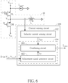
- FIG. 6 is a diagram illustrating a second exemplary design of the current sensing circuit shown in FIG. 1 according to an embodiment of the present invention.
- the processing circuit 104 may be configured to include an adjustment signal generator circuit 602 and a combining circuit 604.
- the adjustment signal generator circuit 602 is arranged to generate an adjustment signal I FF .
- the adjustment signal I FF may be expressed in "voltage" form or "current” form, depending up actual design considerations.
- the adjustment signal generator circuit 602 may generate the adjustment signal I FF according to an average value of the sensed current signal I SEN and the duty cycle D controlled by the current-mode PWM control.
- the adjustment signal generator circuit 602 may generate the adjustment signal I FF according to the load current I LOAD of the DC-to-DC converter, the input voltage V IN of the DC-to-DC converter, and the output voltage V OUT of the DC-to-DC converter.
- the sensed current signal I ASEN includes information of the inductor current I L for current-mode PWM control, but is free from the input-voltage-dependent factor I LOAD 1 ⁇ D that significantly degrades the line transient performance.
- the DC-to-DC converter e.g., inverting buck-boost converter
- retains weighting of current information and current-mode characteristic e.g. saving the hardware compensation cost
- the current sensing circuit 100 shown in FIG. 6 can be implemented using a single circuit design.
- FIG. 5 and FIG. 6 are for illustrative purposes only, and are not meant to be limitations of the present invention.
- the sensed current signal I ASEN (which is derived from the sensed current signal I SEN ) has an average value being a constant under different input voltages V IN , the variation ⁇ V COMP of the error signal V COMP can be mitigated to reduce the output voltage variation, as illustrated in FIG. 4 .
- any current-mode PWM controller using the sensed current signal I ASEN with a constant average value falls within the scope of the present invention.
- the DC-to-DC converter using the proposed current-mode control design is an inverting buck-boost converter.
- this is not meant to be a limitation of the present invention.
- any DC-to-DC converter using the sensed current signal I ASEN for current-mode PWM control falls within the scope of the present invention.
Landscapes
- Engineering & Computer Science (AREA)
- Power Engineering (AREA)
- Physics & Mathematics (AREA)
- General Physics & Mathematics (AREA)
- Dc-Dc Converters (AREA)
- Control Of Motors That Do Not Use Commutators (AREA)
- Electronic Switches (AREA)
Applications Claiming Priority (2)
| Application Number | Priority Date | Filing Date | Title |
|---|---|---|---|
| US202063054842P | 2020-07-22 | 2020-07-22 | |
| US17/368,782 US11581795B2 (en) | 2020-07-22 | 2021-07-06 | Current sensing circuit for generating sensed current signal with average value being constant under different input voltages of direct current to direct current converter and associated current-mode control circuit |
Publications (1)
| Publication Number | Publication Date |
|---|---|
| EP3944480A1 true EP3944480A1 (de) | 2022-01-26 |
Family
ID=76958884
Family Applications (1)
| Application Number | Title | Priority Date | Filing Date |
|---|---|---|---|
| EP21186245.3A Pending EP3944480A1 (de) | 2020-07-22 | 2021-07-16 | Stromsensorschaltung zur erzeugung eines abgetasteten stromsignals mit konstantem mittelwert bei unterschiedlichen eingangsspannungen eines gleichstromwandlers und zugehörige strommodenregelschaltung |
Country Status (4)
| Country | Link |
|---|---|
| US (1) | US11581795B2 (de) |
| EP (1) | EP3944480A1 (de) |
| CN (1) | CN113972841B (de) |
| TW (1) | TWI783564B (de) |
Families Citing this family (4)
| Publication number | Priority date | Publication date | Assignee | Title |
|---|---|---|---|---|
| US12062984B2 (en) * | 2021-07-14 | 2024-08-13 | Stmicroelectronics S.R.L. | Method of operating a converter circuit, corresponding converter circuit and driver device |
| US12003177B2 (en) | 2022-05-19 | 2024-06-04 | Stmicroelectronics S.R.L. | Method and apparatus for sensing output current in a DC-DC converter circuit |
| US12438463B2 (en) | 2022-05-19 | 2025-10-07 | Stmicroelectronics S.R.L. | Method and apparatus for sensing inductor input/output current in a DC-DC converter circuit |
| US12413131B2 (en) | 2022-05-19 | 2025-09-09 | Stmicroelectronics S.R.L. | Method and apparatus for sensing inductor input/output current in a DC-DC converter circuit |
Citations (2)
| Publication number | Priority date | Publication date | Assignee | Title |
|---|---|---|---|---|
| US4987361A (en) * | 1988-11-12 | 1991-01-22 | Ant Nachrichtentechnik Gmbh | Switching regulator having a constant current through its inductance |
| EP1889135B1 (de) * | 2005-04-19 | 2012-08-22 | Raytheon Company | Verfahren und steuerschaltkreise zur bereitstellung einer durchschnittsstrommodensteuerung in einem stromwandler und aktives stromfilter |
Family Cites Families (15)
| Publication number | Priority date | Publication date | Assignee | Title |
|---|---|---|---|---|
| US6459602B1 (en) * | 2000-10-26 | 2002-10-01 | O2 Micro International Limited | DC-to-DC converter with improved transient response |
| US7425819B2 (en) * | 2005-06-16 | 2008-09-16 | Microsemi Corporation | Slope compensation circuit |
| US8305055B2 (en) * | 2010-01-29 | 2012-11-06 | Intersil Americas Inc. | Non-inverting buck boost voltage converter |
| TWI460970B (zh) | 2010-04-02 | 2014-11-11 | Leadtrend Tech Corp | 適應性斜率補償模組及其方法 |
| TWI399909B (zh) | 2010-04-09 | 2013-06-21 | Alpha & Omega Semiconductor Cayman Ltd | Power conversion system and power control method for reducing mutual regulation effect |
| US8829879B2 (en) * | 2010-12-03 | 2014-09-09 | Maxim Integrated Products, Inc. | Inductor current measurement for DC to DC converters |
| CN103187854B (zh) * | 2011-12-31 | 2016-01-20 | 意法半导体研发(深圳)有限公司 | 用于控制电源转换器中的dcm-ccm振荡的系统和方法 |
| TW201351861A (zh) * | 2012-06-08 | 2013-12-16 | Novatek Microelectronics Corp | 控制電源轉換裝置的方法及其相關電路 |
| CN103683932B (zh) * | 2012-09-11 | 2016-08-03 | 晶豪科技股份有限公司 | 脉宽调制模式或脉冲省略模式下的电压转换器及切换方法 |
| TWI473407B (zh) * | 2012-09-19 | 2015-02-11 | Univ Nat Cheng Kung | 非反向—升降壓兩用型直流轉直流數位控制系統 |
| CN105392231B (zh) | 2015-12-03 | 2017-10-31 | 昂宝电子(上海)有限公司 | 用于向一个或多个发光二极管提供输出电流的系统 |
| US9954440B2 (en) * | 2016-05-13 | 2018-04-24 | Mediatek Inc. | Controller for DC/DC power converters |
| US10170985B1 (en) * | 2017-12-06 | 2019-01-01 | National Chung Shan Institute Of Science And Technology | Apparatus for current estimation of DC/DC converter and DC/DC converter assembly |
| US10958167B2 (en) * | 2018-08-08 | 2021-03-23 | Qualcomm Incorporated | Current sensing in an on-die direct current-direct current (DC-DC) converter for measuring delivered power |
| CN110677043B (zh) * | 2019-09-12 | 2021-05-28 | 无锡江南计算技术研究所 | 一种输出电压自适应调节的多相dcdc电源控制电路 |
-
2021
- 2021-07-06 US US17/368,782 patent/US11581795B2/en active Active
- 2021-07-07 TW TW110124962A patent/TWI783564B/zh active
- 2021-07-08 CN CN202110772669.2A patent/CN113972841B/zh active Active
- 2021-07-16 EP EP21186245.3A patent/EP3944480A1/de active Pending
Patent Citations (2)
| Publication number | Priority date | Publication date | Assignee | Title |
|---|---|---|---|---|
| US4987361A (en) * | 1988-11-12 | 1991-01-22 | Ant Nachrichtentechnik Gmbh | Switching regulator having a constant current through its inductance |
| EP1889135B1 (de) * | 2005-04-19 | 2012-08-22 | Raytheon Company | Verfahren und steuerschaltkreise zur bereitstellung einer durchschnittsstrommodensteuerung in einem stromwandler und aktives stromfilter |
Non-Patent Citations (2)
| Title |
|---|
| RICHARD REDL ET AL: "Near-Optimum Dynamic Regulation of DC-DC Converters Using Feed-Forward of Output Current and Input Voltage with Current-Mode Control", IEEE TRANSACTIONS ON POWER ELECTRONICS, INSTITUTE OF ELECTRICAL AND ELECTRONICS ENGINEERS, USA, vol. 23, no. 3, 1 July 1986 (1986-07-01), pages 181 - 192, XP011242282, ISSN: 0885-8993 * |
| YUSHAN LI ET AL: "Current Mode Control for Boost Converters With Constant Power Loads", IEEE TRANSACTIONS ON CIRCUITS AND SYSTEMS I: REGULAR PAPERS, IEEE, US, vol. 59, no. 1, 1 January 2012 (2012-01-01), pages 198 - 206, XP011391862, ISSN: 1549-8328, DOI: 10.1109/TCSI.2011.2161364 * |
Also Published As
| Publication number | Publication date |
|---|---|
| TW202205796A (zh) | 2022-02-01 |
| US11581795B2 (en) | 2023-02-14 |
| US20220029520A1 (en) | 2022-01-27 |
| TWI783564B (zh) | 2022-11-11 |
| CN113972841A (zh) | 2022-01-25 |
| CN113972841B (zh) | 2025-10-03 |
Similar Documents
| Publication | Publication Date | Title |
|---|---|---|
| US11581795B2 (en) | Current sensing circuit for generating sensed current signal with average value being constant under different input voltages of direct current to direct current converter and associated current-mode control circuit | |
| US7898235B2 (en) | Method and apparatus to control voltage conversion mode | |
| CN101610033B (zh) | Dc-dc变换器 | |
| US8982585B2 (en) | Systems and methods for primary-side regulation in off-line switching-mode flyback power conversion system | |
| US7411316B2 (en) | Dual-input power converter and control methods thereof | |
| US8013585B2 (en) | DC-DC converter and DC-DC power conversion method employing overcurrent protection | |
| US20090174384A1 (en) | Switching regulator and method of controlling the same | |
| US8570006B2 (en) | Device and method for controlling a buck-boost converter | |
| US8837175B2 (en) | Systems and methods for adaptive switching frequency control in switching-mode power conversion systems | |
| US7528589B2 (en) | Step-up DC/DC converter and electronic appliance therewith | |
| KR100744592B1 (ko) | Dc-dc 컨버터, dc-dc 컨버터의 제어 회로 및dc-dc 컨버터의 제어 방법 | |
| US7031174B2 (en) | DC-to-DC converter with improved transient response | |
| US8981752B2 (en) | Energy-based oriented switching mode power supply | |
| JP2010154655A (ja) | 電源システム | |
| US12542489B2 (en) | DC/DC converter control circuit, power supply circuit and electronic device | |
| KR20070100389A (ko) | 스위칭 레귤레이터 및 이것을 구비한 전자 기기 | |
| US7423414B1 (en) | Apparatus and method for switching regulator with compensation delay for output voltage error correction | |
| US12057764B2 (en) | Systems and methods for a controller for reducing power loss of power converters | |
| JP4467395B2 (ja) | 電源装置 | |
| US10230301B2 (en) | Non-isolated DC/DC converter | |
| TWI405392B (zh) | 電壓轉換器 | |
| JP4545526B2 (ja) | 電源制御用半導体集積回路およびスイッチング電源装置 | |
| JP4282673B2 (ja) | スイッチング電源装置 | |
| US20250343484A1 (en) | Dc-dc converter | |
| US7295082B2 (en) | Pulse frequency modulation oscillating circuit for a DC/DC converter |
Legal Events
| Date | Code | Title | Description |
|---|---|---|---|
| PUAI | Public reference made under article 153(3) epc to a published international application that has entered the european phase |
Free format text: ORIGINAL CODE: 0009012 |
|
| STAA | Information on the status of an ep patent application or granted ep patent |
Free format text: STATUS: THE APPLICATION HAS BEEN PUBLISHED |
|
| AK | Designated contracting states |
Kind code of ref document: A1 Designated state(s): AL AT BE BG CH CY CZ DE DK EE ES FI FR GB GR HR HU IE IS IT LI LT LU LV MC MK MT NL NO PL PT RO RS SE SI SK SM TR |
|
| STAA | Information on the status of an ep patent application or granted ep patent |
Free format text: STATUS: REQUEST FOR EXAMINATION WAS MADE |
|
| 17P | Request for examination filed |
Effective date: 20220718 |
|
| RBV | Designated contracting states (corrected) |
Designated state(s): AL AT BE BG CH CY CZ DE DK EE ES FI FR GB GR HR HU IE IS IT LI LT LU LV MC MK MT NL NO PL PT RO RS SE SI SK SM TR |
|
| P01 | Opt-out of the competence of the unified patent court (upc) registered |
Effective date: 20230607 |
|
| STAA | Information on the status of an ep patent application or granted ep patent |
Free format text: STATUS: EXAMINATION IS IN PROGRESS |
|
| 17Q | First examination report despatched |
Effective date: 20240603 |