EP3937372A1 - Oszillator und vorrichtung - Google Patents
Oszillator und vorrichtung Download PDFInfo
- Publication number
- EP3937372A1 EP3937372A1 EP19923064.0A EP19923064A EP3937372A1 EP 3937372 A1 EP3937372 A1 EP 3937372A1 EP 19923064 A EP19923064 A EP 19923064A EP 3937372 A1 EP3937372 A1 EP 3937372A1
- Authority
- EP
- European Patent Office
- Prior art keywords
- voltage
- oscillator
- mos transistor
- coupled
- power supply
- Prior art date
- Legal status (The legal status is an assumption and is not a legal conclusion. Google has not performed a legal analysis and makes no representation as to the accuracy of the status listed.)
- Pending
Links
- 239000003990 capacitor Substances 0.000 claims description 30
- 230000010355 oscillation Effects 0.000 abstract description 25
- 238000005516 engineering process Methods 0.000 abstract description 7
- 238000010586 diagram Methods 0.000 description 16
- 101100013558 Arabidopsis thaliana FTSH2 gene Proteins 0.000 description 12
- 101100503482 Arabidopsis thaliana FTSH5 gene Proteins 0.000 description 12
- 101150082136 VAR1 gene Proteins 0.000 description 12
- 238000004891 communication Methods 0.000 description 3
- 230000009286 beneficial effect Effects 0.000 description 2
- 238000005265 energy consumption Methods 0.000 description 2
- 229910044991 metal oxide Inorganic materials 0.000 description 2
- 150000004706 metal oxides Chemical class 0.000 description 2
- 239000004065 semiconductor Substances 0.000 description 2
- 230000001413 cellular effect Effects 0.000 description 1
- 239000013256 coordination polymer Substances 0.000 description 1
- 230000008878 coupling Effects 0.000 description 1
- 238000010168 coupling process Methods 0.000 description 1
- 238000005859 coupling reaction Methods 0.000 description 1
- 230000007423 decrease Effects 0.000 description 1
- 238000007599 discharging Methods 0.000 description 1
- 238000010295 mobile communication Methods 0.000 description 1
- 230000008054 signal transmission Effects 0.000 description 1
- 239000000758 substrate Substances 0.000 description 1
Images



Classifications
-
- H—ELECTRICITY
- H03—ELECTRONIC CIRCUITRY
- H03B—GENERATION OF OSCILLATIONS, DIRECTLY OR BY FREQUENCY-CHANGING, BY CIRCUITS EMPLOYING ACTIVE ELEMENTS WHICH OPERATE IN A NON-SWITCHING MANNER; GENERATION OF NOISE BY SUCH CIRCUITS
- H03B5/00—Generation of oscillations using amplifier with regenerative feedback from output to input
- H03B5/08—Generation of oscillations using amplifier with regenerative feedback from output to input with frequency-determining element comprising lumped inductance and capacitance
- H03B5/12—Generation of oscillations using amplifier with regenerative feedback from output to input with frequency-determining element comprising lumped inductance and capacitance active element in amplifier being semiconductor device
- H03B5/1206—Generation of oscillations using amplifier with regenerative feedback from output to input with frequency-determining element comprising lumped inductance and capacitance active element in amplifier being semiconductor device using multiple transistors for amplification
- H03B5/1212—Generation of oscillations using amplifier with regenerative feedback from output to input with frequency-determining element comprising lumped inductance and capacitance active element in amplifier being semiconductor device using multiple transistors for amplification the amplifier comprising a pair of transistors, wherein an output terminal of each being connected to an input terminal of the other, e.g. a cross coupled pair
-
- H—ELECTRICITY
- H03—ELECTRONIC CIRCUITRY
- H03B—GENERATION OF OSCILLATIONS, DIRECTLY OR BY FREQUENCY-CHANGING, BY CIRCUITS EMPLOYING ACTIVE ELEMENTS WHICH OPERATE IN A NON-SWITCHING MANNER; GENERATION OF NOISE BY SUCH CIRCUITS
- H03B5/00—Generation of oscillations using amplifier with regenerative feedback from output to input
- H03B5/02—Details
- H03B5/04—Modifications of generator to compensate for variations in physical values, e.g. power supply, load, temperature
-
- H—ELECTRICITY
- H03—ELECTRONIC CIRCUITRY
- H03B—GENERATION OF OSCILLATIONS, DIRECTLY OR BY FREQUENCY-CHANGING, BY CIRCUITS EMPLOYING ACTIVE ELEMENTS WHICH OPERATE IN A NON-SWITCHING MANNER; GENERATION OF NOISE BY SUCH CIRCUITS
- H03B5/00—Generation of oscillations using amplifier with regenerative feedback from output to input
- H03B5/08—Generation of oscillations using amplifier with regenerative feedback from output to input with frequency-determining element comprising lumped inductance and capacitance
- H03B5/12—Generation of oscillations using amplifier with regenerative feedback from output to input with frequency-determining element comprising lumped inductance and capacitance active element in amplifier being semiconductor device
- H03B5/1228—Generation of oscillations using amplifier with regenerative feedback from output to input with frequency-determining element comprising lumped inductance and capacitance active element in amplifier being semiconductor device the amplifier comprising one or more field effect transistors
-
- H—ELECTRICITY
- H03—ELECTRONIC CIRCUITRY
- H03B—GENERATION OF OSCILLATIONS, DIRECTLY OR BY FREQUENCY-CHANGING, BY CIRCUITS EMPLOYING ACTIVE ELEMENTS WHICH OPERATE IN A NON-SWITCHING MANNER; GENERATION OF NOISE BY SUCH CIRCUITS
- H03B5/00—Generation of oscillations using amplifier with regenerative feedback from output to input
- H03B5/08—Generation of oscillations using amplifier with regenerative feedback from output to input with frequency-determining element comprising lumped inductance and capacitance
- H03B5/12—Generation of oscillations using amplifier with regenerative feedback from output to input with frequency-determining element comprising lumped inductance and capacitance active element in amplifier being semiconductor device
- H03B5/1237—Generation of oscillations using amplifier with regenerative feedback from output to input with frequency-determining element comprising lumped inductance and capacitance active element in amplifier being semiconductor device comprising means for varying the frequency of the generator
- H03B5/124—Generation of oscillations using amplifier with regenerative feedback from output to input with frequency-determining element comprising lumped inductance and capacitance active element in amplifier being semiconductor device comprising means for varying the frequency of the generator the means comprising a voltage dependent capacitance
- H03B5/1243—Generation of oscillations using amplifier with regenerative feedback from output to input with frequency-determining element comprising lumped inductance and capacitance active element in amplifier being semiconductor device comprising means for varying the frequency of the generator the means comprising a voltage dependent capacitance the means comprising voltage variable capacitance diodes
-
- H—ELECTRICITY
- H03—ELECTRONIC CIRCUITRY
- H03L—AUTOMATIC CONTROL, STARTING, SYNCHRONISATION OR STABILISATION OF GENERATORS OF ELECTRONIC OSCILLATIONS OR PULSES
- H03L1/00—Stabilisation of generator output against variations of physical values, e.g. power supply
- H03L1/02—Stabilisation of generator output against variations of physical values, e.g. power supply against variations of temperature only
Definitions
- This application relates to the field of electronic technologies, and in particular, to an oscillator and a device.
- phase-locked loop (phase-locked loop, PLL) is an important element in a communications system, and is widely used.
- the phase-locked loop mainly includes a charge pump analog phase-locked loop (charge pump phase-locked loop, CPPLL) based on a voltage-controlled oscillator (voltage-controlled oscillator, VCO) and an all-digital phase-locked loop (All-Digital Phase-Locked Loop, ADPLL) based on a digitally-controlled oscillator (digitally-controlled oscillator, DCO).
- the oscillator (VCO/DCO) is a core element of the phase-locked loop. Functions and performance of the oscillator directly affect functions and performance of the phase-locked loop.
- an oscillation frequency of the oscillator changes with an external environment.
- the oscillation frequency of the oscillator decreases as a temperature increases. Therefore, the phase-locked loop needs an additional compensation circuit for frequency compensation, to keep an output frequency unchanged.
- the CPPLL or the ADPLL uses the additional compensation circuit for frequency compensation
- a large quantity of varactors need to be disposed inside the VCO of the CPPLL or the DCO of the ADPLL, to ensure a relatively wide frequency compensation range of the oscillator (VCO/DCO) by using the large quantity of varactors.
- the large quantity of varactors cause performance of the oscillator (VCO/DCO) such as phase noise and spur to deteriorate, and also occupy a relatively large area, thereby increasing a design difficulty of the oscillator.
- This application provides an oscillator and a device using the oscillator, to improve performance of the oscillator, reduce an occupied area of the oscillator, and simplify a design of the oscillator.
- an oscillator including: a resonant circuit, configured to generate an oscillator signal; a first cross-coupled transistor, coupled to the resonant circuit; and a power supply circuit, configured to supply a power supply signal for the first cross-coupled transistor based on a first voltage and a second voltage, where the first voltage is a power supply voltage, and the second voltage is a voltage generated by an external sensing circuit.
- the oscillation frequency of the oscillator changes with the power supply signal of the first cross-coupled transistor in the oscillator, the oscillation frequency of the oscillator can be compensated by adjusting the power supply signal, so that performance of the oscillator is improved. Compared with the conventional technology, this can reduce an occupied area of the oscillator and simply a design of the oscillator because a large quantity of varactors do not need to be disposed inside the oscillator for frequency compensation.
- the first voltage is a fixed voltage
- the second voltage is a variable voltage
- the power supply signal is controlled by the fixed voltage and the variable voltage, so that the oscillation frequency of the oscillator can be compensated by using the variable voltage. This improves the performance of the oscillator.
- the fixed voltage is a positive voltage of a fixed power supply, or the fixed voltage is a negative voltage of a fixed power supply.
- the power supply signal supplied by the power supply circuit is a voltage signal or a current signal.
- the power supply circuit includes an adder, and the adder is configured to add the first voltage and the second voltage to obtain the voltage signal.
- the power supply circuit includes a power supply transistor, a source of the power supply transistor is configured to receive the first voltage, a gate of the power supply transistor is configured to receive the second voltage, and a drain of the power supply transistor is configured to output the current signal.
- the external sensing circuit is configured to generate the second voltage based on a temperature, or the external sensing circuit is configured to generate the second voltage based on a mechanical pressure, or the external sensing circuit is configured to generate the second voltage based on a mechanical vibration.
- the external sensing circuit can compensate for the oscillation frequency of the oscillator based on different parameters of an external environment in which the oscillator is located, thereby improving the performance of the oscillator.
- the first cross-coupled transistor includes a first MOS transistor and a second MOS transistor.
- a source of the first MOS transistor and a source of the second MOS transistor are coupled to a first node.
- a gate of the first MOS transistor, a drain of the second MOS transistor, and a first terminal of the resonant circuit are coupled to a second node.
- a drain of the first MOS transistor, a gate of the second MOS transistor, and a second terminal of the resonant circuit are coupled to a third node.
- the first node is configured to receive the power supply signal.
- a simple and effective implementation of the first cross-coupled transistor is provided. Therefore, complexity of the oscillator can be simplified, and the occupied area of the oscillator can be reduced.
- the oscillator further includes a second cross-coupled transistor.
- the second cross-coupled transistor includes a third MOS transistor and a fourth MOS transistor.
- a source of the third MOS transistor and a source of the fourth MOS transistor are coupled to a fourth node.
- a gate of the third MOS transistor, a drain of the fourth MOS transistor, and the first terminal of the resonant circuit are coupled to the second node.
- a drain of the third MOS transistor, a gate of the fourth MOS transistor, and the second terminal of the resonant circuit are coupled to the third node.
- the fourth node is coupled to a positive terminal or a negative terminal of power supply.
- the provided implementation of the cross-coupled transistor can improve the performance of the oscillator.
- the resonant circuit includes an inductor, a first varactor, a second varactor, and a switched capacitor array. Two terminals of the inductor are coupled to the second node and the third node. One terminal of the first varactor is coupled to one terminal of the second varactor, and the other terminal of the first varactor and the other terminal of the second varactor are respectively coupled to the second node and the third node. Two terminals of the switched capacitor array are coupled to the second node and the third node.
- a simple and effective implementation of the resonant circuit is provided. Therefore, the complexity of the oscillator can be simplified, and the occupied area of the oscillator can be reduced.
- the oscillator further includes: a digital-to-analog converter, configured to: when a voltage generated by the external sensing circuit is a digital voltage, convert the digital voltage into an analog voltage, to obtain the second voltage.
- a digital-to-analog converter configured to: when a voltage generated by the external sensing circuit is a digital voltage, convert the digital voltage into an analog voltage, to obtain the second voltage.
- the digital-to-analog converter includes a switch array, and a plurality of resistors connected in series with each other between a power supply terminal and a ground terminal. A connection point between two adjacent resistors among the plurality of resistors connected in series with each other is connected to one switch in the switch array.
- the digital-to-analog converter is configured to control a switch that is in the switch array and that corresponds to the digital voltage to be closed, to convert the digital voltage into the analog voltage.
- an oscillator including: a resonant circuit, configured to generate an oscillator signal; and a first cross-coupled circuit, coupled to the resonant circuit.
- the first cross-coupled circuit includes a first MOS transistor and a second MOS transistor that are cross-coupled, and a body of the first MOS transistor and a body of the second MOS transistor are configured to receive a variable control voltage.
- the oscillation frequency of the oscillator changes with a body voltage of the first MOS transistor and a body voltage of the second MOS transistor in the first cross-coupled circuit
- the oscillation frequency of the oscillator can be compensated by adjusting the variable control voltage to adjust the body voltages of the MOS transistors, so that performance of the oscillator can be improved.
- this reduces an occupied area of the oscillator and simplifies a design of the oscillator because a large quantity of varactors do not need to be disposed inside the oscillator.
- variable control voltage is a voltage generated based on at least one of the following parameters: a temperature, a mechanical pressure, or a mechanical vibration.
- the oscillation frequency of the oscillator can be compensated based on different parameters of an external environment in which the oscillator is located, so that the performance of the oscillator is improved.
- variable control voltage is a voltage generated by an external sensing circuit based on a temperature of the oscillator, or the variable control voltage is a voltage generated by an external sensing circuit based on a mechanical pressure of the oscillator, or the variable control voltage is a voltage generated by an external sensing circuit based on a mechanical vibration of the oscillator.
- the body of the first MOS transistor is coupled to the body of the second MOS transistor to receive the variable control voltage.
- a source of the first MOS transistor and a source of the second MOS transistor are coupled to a first node to couple to a first power supply terminal.
- a gate of the first MOS transistor, a drain of the second MOS transistor, and a first terminal of the resonant circuit are coupled to a second node.
- a drain of the first MOS transistor, a gate of the second MOS transistor, and a second terminal of the resonant circuit are coupled to a third node.
- a simple and effective implementation of the first cross-coupled circuit is provided. Therefore, complexity of the oscillator can be simplified, and the occupied area of the oscillator can be reduced.
- the oscillator further includes a second cross-coupled circuit.
- the second cross-coupled transistor includes a third MOS transistor and a fourth MOS transistor that are cross-coupled.
- a gate of the third MOS transistor, a drain of the fourth MOS transistor, and the first terminal of the resonant circuit are coupled to the second node.
- a drain of the third MOS transistor, a gate of the fourth MOS transistor, and the second terminal of the resonant circuit are coupled to the third node.
- a source of the third MOS transistor and a source of the fourth MOS transistor are coupled to a fourth node to couple to a second power supply terminal.
- the performance of the oscillator can be further improved.
- a body of the third MOS transistor and a body of the fourth MOS transistor are coupled to a fifth node, where the fifth node is configured to receive the variable control voltage, or the first node is configured to couple to the second power supply terminal.
- the provided implementation of the second cross-coupled circuit can further improve the performance of the oscillator.
- the resonant circuit includes an inductor, a first varactor, a second varactor, and a switched capacitor array. Two terminals of the inductor are coupled to the second node and the third node. One terminal of the first varactor is coupled to one terminal of the second varactor, and the other terminal of the first varactor and the other terminal of the second varactor are respectively coupled to the second node and the third node. Two terminals of the switched capacitor array are coupled to the second node and the third node.
- a simple and effective implementation of the resonant circuit is provided. Therefore, the complexity of the oscillator can be simplified, and the occupied area of the oscillator can be reduced.
- the oscillator further includes: a digital-to-analog converter, configured to: when a voltage generated by the external sensing circuit is a digital voltage, convert the digital voltage into an analog voltage, to obtain the variable control voltage.
- a digital-to-analog converter configured to: when a voltage generated by the external sensing circuit is a digital voltage, convert the digital voltage into an analog voltage, to obtain the variable control voltage.
- the digital-to-analog converter includes a switch array, and a plurality of resistors connected in series with each other between a power supply terminal and a ground terminal. A connection point between two adjacent resistors among the plurality of resistors connected in series with each other is connected to one switch in the switch array.
- the digital-to-analog converter is configured to control a switch that is in the switch array and that corresponds to the digital voltage to be closed, to convert the digital voltage into the analog voltage.
- a phase-locked loop includes: a phase frequency detector, a filter, an external sensing circuit, and the oscillator provided in any one of the first aspect or the possible implementations of the first aspect.
- the oscillator is configured to generate an oscillator signal.
- the phase frequency detector and the filter are configured to generate, based on the oscillator signal, a loop voltage that meets a specific phase requirement.
- the external sensing circuit is configured to generate a second voltage based on at least one of the following parameters: a temperature, a mechanical pressure, or a mechanical vibration.
- the external sensing circuit is further configured to output the second voltage to the power supply circuit in the oscillator.
- a phase-locked loop includes: a phase frequency detector, a filter, an external sensing circuit, and the oscillator provided in any one of the second aspect or the possible implementations of the second aspect.
- the oscillator is configured to generate an oscillator signal.
- the phase frequency detector and the filter are configured to generate, based on the oscillator signal, a loop voltage that meets a specific phase requirement.
- the external sensing circuit is configured to generate a variable control voltage based on at least one of the following parameters.
- the external sensing circuit is further configured to output the variable control voltage to the bodies of the MOS transistors of the first cross-coupled transistor in the oscillator.
- an oscillator-based apparatus is further provided.
- the apparatus includes a radio frequency circuit and the oscillator provided in any one of the first aspect or the possible implementations of the first aspect.
- the oscillator is configured to supply a local carrier signal for the radio frequency circuit.
- the apparatus may be a terminal, a base station, a chip built in the terminal or the base station, or the like.
- an oscillator-based apparatus is further provided.
- the terminal includes a radio frequency circuit and the oscillator provided in any one of the second aspect or the possible implementations of the second aspect.
- the oscillator is configured to supply a local carrier signal for the radio frequency circuit.
- the apparatus may be a terminal, a base station, a chip built in the terminal or the base station, or the like.
- any one of the foregoing described phase-locked loops includes the foregoing described oscillator. Therefore, for beneficial effects that can be achieved by the any one of the phase-locked loops, refer to beneficial effects of the foregoing described oscillator. Details are not described herein again.
- At least one refers to one or more
- a plurality of refers to two or more than two.
- the term “and/or” describes an association relationship for describing associated objects and represents that three relationships may exist.
- a and/or B may represent the following three cases: Only A exists, both A and B exist, and only B exists, where A and B may be singular or plural.
- At least one of the following items or a similar expression thereof refers to any combination of these items, including a single item or any combination of a plurality of items.
- At least one of a, b, or c may represent: a, b, c, a and b, a and c, b and c, or a, b, and c, where a, b, and c may be singular or plural.
- the character “/” generally indicates an "or” relationship between the associated objects.
- the words such as “first” and “second” do not limit a quantity and an execution order.
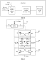
- FIG. 1 is a schematic structural diagram of an oscillator according to an embodiment of this application.
- the oscillator includes a power supply circuit 101, a first cross-coupled transistor 102, and a resonant circuit 103.
- the first cross-coupled transistor 102 is configured to compensate for energy consumption of the resonant circuit 103, namely, negative resistance compensation.
- the resonant circuit 103 is configured to generate an oscillator signal.
- the power supply circuit 101 is configured to supply a power supply signal for the first cross-coupled transistor 102 based on a first voltage V1 and a second voltage V2.
- the power supply signal may be a voltage signal V O obtained by adding the first voltage V1 and the second voltage V2, or the power supply signal is a current signal I O controlled by the first voltage V1 and the second voltage V2.
- the first voltage V1 may be a fixed voltage.
- the fixed voltage may be supplied by a fixed power supply, and the fixed voltage may be a positive voltage VDD supplied by the fixed power supply or a negative voltage VSS (the negative voltage VSS may be specifically a ground terminal GND) supplied by the fixed power supply.
- the second voltage V2 is a variable voltage.
- the second voltage V2 may be generated by an external sensing circuit.
- the second voltage V2 may be a voltage generated by at least one of a temperature sensing circuit, a pressure sensing circuit, or a vibration sensing circuit.
- the external sensing circuit may be configured to generate the second voltage V2 based on a temperature, a mechanical pressure, a mechanical vibration, or the like of an external environment in which the oscillator is located.
- the external sensing circuit generates the second voltage V2 based on a temperature, a mechanical pressure, a mechanical vibration, or the like of a chip in which the oscillator is located.
- the oscillator may be used in a phase-locked loop.
- the external sensing circuit may be configured to compare a reference voltage with a loop voltage of the phase-locked loop to generate the second voltage V2, or the external sensing circuit may be configured to generate the second voltage based on one of the following parameters of the phase-locked loop: a temperature, a mechanical pressure, or a mechanical vibration.
- the temperature sensing circuit may generate a variable voltage based on a change of a temperature of the oscillator or the phase-locked loop using the oscillator
- the pressure sensing circuit may generate a variable voltage based on a change of a mechanical pressure received by the oscillator or the phase-locked loop using the oscillator
- the vibration sensing circuit may generate a variable voltage based on changes of a frequency and magnitude of a vibration received by the oscillator or the phase-locked loop using the oscillator.
- the external sensing circuit may include a sensor, or may include a sensor, another circuit that cooperates with the sensor, and the like.
- the temperature sensing circuit may include a temperature sensor and another circuit other than the temperature sensor in a temperature compensation loop, for example, a comparator.
- the external sensing circuit may further include another sensing circuit.
- the another sensing circuit may be configured to detect a voltage generated by a change of another external factor (an external factor other than the temperature, the mechanical pressure, and the mechanical vibration) that affects an oscillation frequency of the oscillator. This is not specifically limited in this embodiment of this application.
- the power supply circuit 101 may include an adder.
- the adder is configured to: receive the first voltage V1 and the second voltage V2, and add the first voltage V1 and the second voltage V2 to obtain the voltage signal V O .
- the power supply signal is the voltage signal V O .
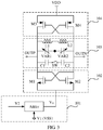
- the oscillator may be shown in FIG. 2 .
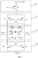
- the oscillator may be shown in FIG. 3 .
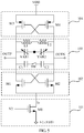
- the power supply circuit 101 may include a power supply transistor M0.
- the power supply transistor may be a voltage-controlled transistor, for example, a metal oxide semiconductor (metal oxide semiconductor, MOS) transistor or an insulated-gate bipolar transistor (insulated-gate bipolar transistor, IGBT).
- MOS metal oxide semiconductor
- IGBT insulated-gate bipolar transistor
- the MOS transistor M0 is configured to: receive the first voltage V1 and the second voltage V2, and generate the current signal I O under control of the first voltage V1 and the second voltage V2. In other words, the first voltage V1 and the second voltage V2 control the MOS transistor M0 to generate the current signal I O when the MOS transistor M0 is turned on.
- the power supply signal is the current signal I O .
- the oscillator may be shown in FIG. 4 .
- the oscillator may be shown in FIG. 5 .
- the MOS transistor M0 included in the power supply circuit 101 may be an NMOS transistor or a PMOS transistor, or may be replaced with another element or circuit having a same function as the power supply MOS transistor M0.
- the power supply MOS transistor M0 is an NMOS transistor is merely an example for description, and this does not constitute any limitation on this embodiment of this application.
- the first cross-coupled transistor 102 may include a first MOS transistor M1 and a second MOS transistor M2.
- a source (source, s) of the first MOS transistor M1 and a source of the second MOS transistor M2 are coupled to a first node.
- a drain (drain, d) of the first MOS transistor M1, a gate (gate, g) of the second MOS transistor M2, and a first terminal of the resonant circuit 103 are coupled to a second node (denoted as OUTP).
- a gate of the first MOS transistor M1, a drain of the second MOS transistor M2, and a second terminal of the resonant circuit 103 are coupled to a third node (denoted as OUTN).
- OUTN and OUTP are configured to output an oscillator signal.
- the power supply circuit 101 includes the adder and the first voltage V1 is the positive voltage VDD supplied by the fixed power supply in FIG. 2 is used for description
- an example in which the power supply circuit 101 includes the adder and the first voltage V1 is the negative voltage VSS supplied by the fixed power supply in FIG. 3 is used for description
- an example in which the power supply circuit 101 includes the MOS transistor M0 and the first voltage V1 is the positive voltage VDD supplied by the fixed power supply in FIG. 4 is used for description
- the oscillator may include one cross-coupled transistor, or may include two cross-coupled transistors: the first cross-coupled transistor 102 and a second cross-coupled transistor 104.
- the second cross-coupled transistor 104 includes a third MOS transistor M3 and a fourth MOS transistor M4.
- a source of the third MOS transistor M3 and a source of the fourth MOS transistor M4 are coupled to a fourth node.
- a drain of the third MOS transistor M3 and a gate of the fourth MOS transistor M4 are coupled to the second node.
- a gate of the third MOS transistor and a drain of the fourth MOS transistor are coupled to the third node.
- the MOS transistors included in the first cross-coupled transistor 102 and the second cross-coupled transistor 104 each may be a cross-coupled pair formed by using NMOS transistors, or may be a cross-coupled pair formed by using PMOS transistors.
- the first cross-coupled transistor 102 and the second cross-coupled transistor 104 are merely examples, and do not constitute any limitation on this embodiment of this application.
- the resonant circuit 103 may include: a first inductor L1, a second inductor L2, a first varactor VAR1, a second varactor VAR2, and a switched capacitor array.
- the switched capacitor array includes a first capacitor C1 and a second capacitor C2, and one terminal of the first capacitor C1 is connected to one terminal of the second capacitor C2 by using a switch (SW) is used for description.
- One terminal of the first varactor VAR1 is coupled to one terminal of the second varactor VAR2.
- One terminal of the first inductor L1 is coupled to one terminal of the second inductor L2.
- the other terminal of the first inductor L1, the other terminal of the first varactor VAR1, and one terminal of the switched capacitor array (which is specifically the other terminal of the first capacitor C1) are all coupled to OUTP.
- the other terminal of the second inductor L2, the other terminal of the second varactor VAR2, and the other terminal of the switched capacitor array (which is specifically the other terminal of the second capacitor C2) are all coupled to OUTN.
- the resonant circuit 103 may be alternatively a circuit of another structure.
- the first inductor L1 and the second inductor L2 are implemented by using one inductor, and the switched capacitor array is a capacitor array of another form.
- the specific structure of the resonant circuit 103 in FIG. 2 to FIG. 5 is merely an example, and does not constitute any limitation on this embodiment of this application.
- the oscillator may be a voltage-controlled oscillator (voltage-controlled oscillator, VCO) or a digitally-controlled oscillator (digitally-controlled oscillator, DCO).
- VCO voltage-controlled oscillator
- DCO digitally-controlled oscillator
- the first varactor VAR1 and the second varactor VAR2 in the resonant circuit 103 may be specifically controlled by an analog signal.
- the oscillator is the DCO
- the first varactor VAR1 and the second varactor VAR2 in the resonant circuit 103 may be specifically controlled by a digital signal.
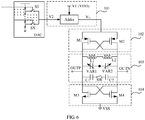
- the oscillator when the oscillator is the DCO, the oscillator may further include a digital-to-analog converter (digital-to-analog converter, DAC).
- the DAC is configured to convert a digital voltage generated by the external sensing circuit into an analog voltage, to obtain the second voltage V2, where details are shown in FIG. 6 and FIG. 7 .
- FIG. 6 and FIG. 7 an example in which the first voltage V1 is the positive voltage VDD supplied by the fixed power supply is used for description.
- the DAC is also applicable to an oscillator in which the first voltage V1 is the negative voltage VSS supplied by the fixed power supply. This is not described in detail in this embodiment of this application again.
- the analog-to-digital converter includes a switch array, and a plurality of resistors connected in series with each other between a power supply terminal and a ground terminal. A connection point between two adjacent resistors among the plurality of resistors connected in series with each other is connected to one switch in the switch array.
- the analog-to-digital converter is configured to control a switch that is in the switch array and that corresponds the digital voltage to be closed, to convert the digital voltage into the analog voltage.
- SO represents the first switch in the switch array
- SX represents the last switch in the switch array.
- the power supply signal of the oscillator is formed by the fixed first voltage V1 and the variable second voltage V2. Therefore, when the oscillation frequency of the oscillator drifts because of an external factor and the like, the oscillation frequency of the oscillator can be compensated by adjusting the power supply signal, so that performance of the oscillator can be improved. Compared with the conventional technology, this reduces an occupied area of the oscillator and simplifies a design difficulty of the oscillator because a large quantity of varactors do not need to be disposed inside the oscillator.
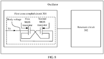
- FIG. 8 is a schematic structural diagram of an oscillator according to an embodiment of this application.
- the oscillator includes a first cross-coupled circuit 301 and a resonant circuit 302.
- the first cross-coupled circuit 301 is configured to compensate for energy consumption of the resonant circuit 302, namely, negative resistance compensation.
- the resonant circuit 302 is configured to generate an oscillator signal.
- the first cross-coupled circuit 301 includes a first MOS transistor and a second MOS transistor that are cross-coupled, and a body (body) of the first MOS transistor and a body of the second MOS transistor are configured to receive a variable control voltage Vt.
- a voltage of the body (namely, a body voltage) of the first MOS transistor and a voltage of the body of the second MOS transistor are equal to the variable control voltage Vt.
- the bodies of the MOS transistors herein may specifically refer to poles corresponding to substrates in the MOS transistors.
- the variable control voltage is a voltage generated based on at least one of the following parameters: a temperature, a mechanical pressure, or a mechanical vibration.
- the variable control voltage Vt may be generated by an external sensing circuit.
- the variable control voltage Vt may be a voltage generated by one of a temperature sensing circuit, a pressure sensing circuit, or a vibration sensing circuit.
- the temperature sensing circuit may generate a variable voltage based on a change of a temperature of the oscillator
- the pressure sensing circuit may generate a variable voltage based on a change of a mechanical pressure received by the oscillator
- the vibration sensing circuit may generate a variable voltage based on changes of a frequency and magnitude of a vibration received by the oscillator.
- the external sensing circuit may be configured to generate the variable control voltage Vt based on a temperature, a mechanical pressure, a mechanical vibration, or the like of an external environment in which the oscillator is located.
- the external sensing circuit generates the variable control voltage Vt based on a temperature, a mechanical pressure, a mechanical vibration, or the like of a chip in which the oscillator is located.
- the oscillator may be used in a phase-locked loop.
- the external sensing circuit may be configured to compare a reference voltage with a loop voltage of the phase-locked loop to generate the variable control voltage Vt, or the variable control voltage Vt may be a voltage generated based on at least one of the following parameters of the phase-locked loop: a temperature, a mechanical pressure, or a mechanical vibration.
- the external sensing circuit may further include another sensing circuit.
- the another sensing circuit may be configured to detect a voltage generated by a change of another external factor (an external factor other than the temperature, the mechanical pressure, and the mechanical vibration) that affects an oscillation frequency of the oscillator. This is not specifically limited in this embodiment of this application.
- the first cross-coupled circuit 301 may include a first MOS transistor M1 and a second MOS transistor M2.
- a source of the first MOS transistor M1 and a source of the second MOS transistor M2 are coupled to a first node.
- a drain of the first MOS transistor M1, a gate of the second MOS transistor M2, and a first terminal of the resonant circuit 302 are coupled to a second node (denoted as OUTP).
- a gate of the first MOS transistor M1, a drain of the second MOS transistor M2, and a second terminal of the resonant circuit 302 are coupled to a third node (denoted as OUTN).
- OUTN and OUTP are configured to output an oscillator signal.
- the oscillator may include one cross-coupled circuit, or may include two cross-coupled circuits: the first cross-coupled circuit 301 and a second cross-coupled circuit 303.
- the second cross-coupled circuit 303 includes a third MOS transistor M3 and a fourth MOS transistor M4.
- a source of the third MOS transistor M3 and a source of the fourth MOS transistor M4 are coupled to a fourth node.
- a drain of the third MOS transistor M3 and a gate of the fourth MOS transistor M4 are coupled to OUT.
- a gate of the third MOS transistor and a drain of the fourth MOS transistor are coupled to OUTN.
- the first node is configured to receive a constant positive voltage VDD
- the fourth node is configured to receive a constant negative voltage VSS (the negative voltage VSS may be specifically a ground terminal GND).
- variable control voltage Vt may be used as a body (body) voltage of the first MOS transistor M1 and a body voltage of the second MOS transistor M2 in the first cross-coupled circuit 301.
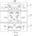
- a body of the third MOS transistor M3 and a body of the fourth MOS transistor M4 in the second cross-coupled circuit 302 may be connected to the VSS, where details are shown in FIG. 9 .
- the variable control voltage Vt may be used to control a body (body) voltage of the first MOS transistor M1 and a body voltage of the second MOS transistor M2 in the first cross-coupled circuit 301.
- a body of the third MOS transistor M3 and a body of the fourth MOS transistor M4 in the second cross-coupled circuit 302 may be connected to the VDD, where details are shown in FIG. 10 .
- the variable control voltage Vt may be used to control a body (body) voltage of the first MOS transistor M1 and a body voltage of the second MOS transistor M2 in the first cross-coupled circuit 301, and control a body (body) voltage of the third MOS transistor M3 and a body voltage of the fourth MOS transistor M4 in the second cross-coupled circuit 303, where details are shown in FIG. 11 .
- the MOS transistors included in the first cross-coupled circuit 301 and the second cross-coupled circuit 303 each may be a cross-coupled pair formed by using NMOS transistors, or may be a cross-coupled pair formed by using PMOS transistors.
- the first cross-coupled circuit 301 and the second cross-coupled circuit 303 in FIG. 9 to FIG. 11 are merely examples, and do not constitute any limitation on this embodiment of this application.
- the resonant circuit 302 may include: a first inductor L1, a second inductor L2, a first varactor VAR1, a second varactor VAR2, and a switched capacitor array.
- the switched capacitor array includes a first capacitor C1 and a second capacitor C2, and one terminal of the first capacitor C1 is connected to one terminal of the second capacitor C2 by using a switch (SW) is used for description.
- One terminal of the first varactor VAR1 is coupled to one terminal of the second varactor VAR2.
- One terminal of the first inductor L1 is coupled to one terminal of the second inductor L2.
- the other terminal of the first inductor L1, the other terminal of the first varactor VAR1, and one terminal of the switched capacitor array (which is specifically the other terminal of the first capacitor C1) are all coupled to OUTP.
- the other terminal of the second inductor L2, the other terminal of the second varactor VAR2, and the other terminal of the switched capacitor array (which is specifically the other terminal of the second capacitor C2) are all coupled to OUTN.
- the resonant circuit 302 may be alternatively a circuit of another structure.
- the first inductor L1 and the second inductor L2 are implemented by using one inductor, and the switched capacitor array is a capacitor array of another form.
- the specific structure of the resonant circuit 302 in FIG. 9 to FIG. 11 is merely an example, and does not constitute any limitation on this embodiment of this application.
- the oscillator may be a voltage-controlled oscillator VCO or a digitally-controlled oscillator DCO.
- the first varactor VAR1 and the second varactor VAR2 in the resonant circuit 302 may be specifically controlled by an analog signal.
- the oscillator is the DCO, the first varactor VAR1 and the second varactor VAR2 in the resonant circuit 302 may be specifically controlled by a digital signal.
- the oscillator when the oscillator is the DCO, the oscillator may further include a DAC.
- the DAC is configured to convert a digital voltage generated by the external sensing circuit into an analog voltage, where details are shown in FIG. 12 . It should be noted that, in FIG. 12 , an example in which the variable control voltage Vt is used to control the body (body) voltage of the first MOS transistor M1 and the body voltage of the second MOS transistor M2 is merely used for description.
- the DAC is also applicable to the oscillator shown in FIG. 10 and FIG. 11 , and details are not described in this embodiment of this application.
- the analog-to-digital converter includes a switch array, and a plurality of resistors connected in series with each other between a power supply terminal and a ground terminal. A connection point between two adjacent resistors among the plurality of resistors connected in series with each other is connected to one switch in the switch array.
- the analog-to-digital converter is configured to control a switch that is in the switch array and that corresponds the digital voltage to be closed, to convert the digital voltage into the analog voltage.
- SO represents the first switch in the switch array
- SX represents the last switch in the switch array.
- the oscillation frequency of the oscillator changes with the body (body) voltages of the cross-coupled MOS transistors in the first cross-coupled circuit 301
- the body (body) voltages of the MOS transistors in the first cross-coupled circuit 301 are controlled by the variable control voltage Vt. Therefore, when the oscillation frequency of the oscillator drifts because of an external factor and the like, the oscillation frequency of the oscillator can be compensated by adjusting the variable control voltage Vt, so that performance of the oscillator can be improved.
- this reduces an occupied area of the oscillator, and simplifies a design of the oscillator because a large quantity of varactors do not need to be disposed inside the oscillator.
- the oscillator shown in FIG. 1 to FIG. 12 may be used in a phase-locked loop, and the phase-locked loop may include a phase frequency detector, a filter, and an oscillator.
- the phase-locked loop may be an analog phase-locked loop.
- the phase-locked loop may be a digital phase-locked loop. Based on this, an embodiment of this application further provides a phase-locked loop.
- the phase-locked loop may include the oscillator provided in any one of FIG. 1 to FIG. 12 .
- the analog phase-locked loop in which the VCO is located and the temperature sensing circuit may be specifically shown in FIG. 13 .
- a connection point of a phase-locked loop control voltage V PLL in FIG. 13 may be specifically a connection point between the first varactor VAR1 and the second varactor VAR2 in the resonant circuit of the oscillator.
- AMP represents an amplifier (amplifier)
- PFD represents a phase frequency detector (phase frequency detector)
- CP represents a charge pump (charge pump)
- DAC represents a digital-to-analog converter
- SW1 to SW4 represent four switches (switches).
- a specific frequency compensation principle is as follows: When the phase-locked loop (phase lock loop, PLL) is stable, an entire loop of the PLL is in a stable state. In this case, V PLL is unchanged. When a temperature changes, a frequency of the VCO drifts, and the loop of the PLL re-locks an oscillation frequency to compensate for a change caused by the temperature. In this case, V PLL changes. After the change of V PLL is monitored by the AMP of the temperature sensing circuit, the temperature sensing circuit starts to generate a temperature-compensated voltage (namely, a second voltage V2) to compensate for a frequency change of the VCO that is caused by the temperature. In this way, V PLL does not greatly change, and the loop of the PLL does not re-lock the oscillation frequency, thereby implementing continuous locking of the oscillation frequency in the analog phase-locked loop.
- a temperature-compensated voltage namely, a second voltage V2
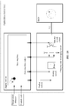
- the digital phase-locked loop in which the DCO is located and the temperature sensing circuit (which may be specifically a temperature detector) may be shown in FIG. 14 .
- a connection point of a control code (FT_code) in FIG. 14 may be specifically a connection point between the first varactor VAR1 and the second varactor VAR2 in the resonant circuit of the oscillator.
- the digital phase-locked loop in FIG. 14 may be divided into a digital portion and an analog portion.
- the digital portion may include a state machine, and the analog portion may include an analog switch, a filter, a charging and discharging circuit, and a selector switch circuit.
- a specific frequency compensation principle is as follows: When the PLL is stable, an entire loop of the PLL is in a stable state. In this case, the control code (FT_code) is unchanged. When a temperature changes, a frequency of the DCO drifts, and the loop of the PLL re-locks an oscillation frequency to compensate for a change caused by the temperature. In this case, the control code (FT_code) changes. After the change of the control code (FT_code) is monitored by the temperature detector, the temperature detector starts to generate a temperature-compensated voltage (namely, a second voltage V2) to compensate for a frequency change of the DCO that is caused by the temperature. In this way, the control code (FT_code) does not greatly change, and the loop of the PLL does not re-lock the oscillation frequency, thereby implementing continuous locking of the oscillation frequency in the digital phase-locked loop.
- An embodiment of this application further provides an oscillator-based apparatus.
- the apparatus may be a terminal, a base station, a chip built in the terminal or the base station, or the like.
- the apparatus may include: a radio frequency circuit, and an oscillator provided in the embodiments of this application.
- the oscillator is configured to supply a local carrier signal for the radio frequency circuit.
- the radio frequency circuit may include any one or a combination of the following: a cellular mobile communications module, a Bluetooth module, a wireless fidelity (Wi-Fi) module, or any radio frequency apparatus requiring a local carrier signal in the terminal.
- the radio frequency circuit in the terminal may be a Bluetooth module and a Wi-Fi module, or may be the Bluetooth module or the Wi-Fi module.
- the radio frequency circuit in the apparatus may be a transceiver, and the apparatus may further include a phase-locked loop.
- the phase-locked loop includes an oscillator, and the oscillator is configured to supply a local carrier signal for the transceiver by using the phase-locked loop.
- the terminal and the base station are merely examples for describing application of an oscillator product provided in the embodiments of this application, and do not limit the application of the oscillator provided in the embodiments of this application.
- the oscillator provided in the embodiments of this application may be used in any scenario in which frequency drift needs to be compensated and any product for which frequency drift needs to be compensated.
- the oscillator, the phase-locked loop, the external sensing circuit, the oscillator-based apparatus, and the like that are disclosed may further be implemented in another manner.
- the described embodiments are merely examples.
- the oscillator division is merely logical function division and may be other division in actual implementation.
- a plurality of components may be combined or integrated into another component, or some features may be ignored or not performed.
- the displayed or discussed mutual signal transmission or communication may be implemented through some interfaces.
- the indirect couplings or communication connections between components or units may be performed in electrical, mechanical, or other forms.
- circuits described as separate parts may or may not be physically separate, and parts displayed as circuit units may be one or more physical units, may be located in one place, or may be distributed on different places. Some or all of the circuits may be selected based on actual requirements to achieve the objectives of the solutions of the embodiments.
Landscapes
- Inductance-Capacitance Distribution Constants And Capacitance-Resistance Oscillators (AREA)
Applications Claiming Priority (1)
| Application Number | Priority Date | Filing Date | Title |
|---|---|---|---|
| PCT/CN2019/081580 WO2020199216A1 (zh) | 2019-04-04 | 2019-04-04 | 一种振荡器及设备 |
Publications (2)
| Publication Number | Publication Date |
|---|---|
| EP3937372A1 true EP3937372A1 (de) | 2022-01-12 |
| EP3937372A4 EP3937372A4 (de) | 2022-03-23 |
Family
ID=72664654
Family Applications (1)
| Application Number | Title | Priority Date | Filing Date |
|---|---|---|---|
| EP19923064.0A Pending EP3937372A4 (de) | 2019-04-04 | 2019-04-04 | Oszillator und vorrichtung |
Country Status (4)
| Country | Link |
|---|---|
| US (1) | US11791772B2 (de) |
| EP (1) | EP3937372A4 (de) |
| CN (1) | CN113615080B (de) |
| WO (1) | WO2020199216A1 (de) |
Families Citing this family (3)
| Publication number | Priority date | Publication date | Assignee | Title |
|---|---|---|---|---|
| CN114584075B (zh) * | 2022-03-11 | 2023-06-06 | 安徽传矽微电子有限公司 | 一种变压器型分布式多核振荡器及其集成电路与终端 |
| TWI838890B (zh) * | 2022-09-29 | 2024-04-11 | 力拓半導體股份有限公司 | 電子裝置以及其溫度偵測裝置 |
| CN116318128A (zh) * | 2023-03-30 | 2023-06-23 | 浙江地芯引力科技有限公司 | 数控振荡电路及振荡装置 |
Family Cites Families (12)
| Publication number | Priority date | Publication date | Assignee | Title |
|---|---|---|---|---|
| US8089324B2 (en) * | 2006-08-05 | 2012-01-03 | Min Ming Tarng | Varactor-free amplitude controlled oscillator(ACO) for system on chip and system on card Xtaless clock SOC |
| US20090021513A1 (en) | 2007-07-18 | 2009-01-22 | Pixblitz Studios Inc. | Method of Customizing 3D Computer-Generated Scenes |
| US20090033428A1 (en) * | 2007-07-30 | 2009-02-05 | Mediatek Singapore Pte Ltd. | Voltage controlled oscillator |
| US9171097B2 (en) | 2009-03-31 | 2015-10-27 | Qualcomm Incorporated | Memoizing web-browsing computation with DOM-based isomorphism |
| CN102508644B (zh) | 2011-09-22 | 2015-04-29 | Tcl集团股份有限公司 | 一种3d用户界面图形引擎系统 |
| CN104242924B (zh) * | 2013-07-26 | 2017-09-22 | 西安电子科技大学 | 具有自动频率校准功能的多频带电感‑电容压控振荡器 |
| US20170126177A1 (en) * | 2015-10-30 | 2017-05-04 | Texas Instruments Incorporated | Trifilar Voltage Controlled Oscillator |
| CN106504305A (zh) | 2016-10-25 | 2017-03-15 | 天脉聚源(北京)传媒科技有限公司 | 一种动画处理方法及装置 |
| CN107066430B (zh) | 2017-04-21 | 2021-02-26 | 阿里巴巴(中国)有限公司 | 图片处理方法、装置、服务端及客户端 |
| CN107464208B (zh) | 2017-07-24 | 2019-07-09 | 浙江大学 | 一种图形绘制流水线中像素着色结果重用方法 |
| CN108768301A (zh) * | 2018-05-08 | 2018-11-06 | 东南大学 | 一种衬底动态偏置的lc压控振荡器 |
| CN108649902B (zh) * | 2018-05-14 | 2024-01-23 | 成都中宇微芯科技有限公司 | 一种温度补偿压控振荡器及补偿方法 |
-
2019
- 2019-04-04 EP EP19923064.0A patent/EP3937372A4/de active Pending
- 2019-04-04 WO PCT/CN2019/081580 patent/WO2020199216A1/zh not_active Ceased
- 2019-04-04 CN CN201980094498.3A patent/CN113615080B/zh active Active
-
2021
- 2021-10-01 US US17/492,463 patent/US11791772B2/en active Active
Also Published As
| Publication number | Publication date |
|---|---|
| CN113615080A (zh) | 2021-11-05 |
| US20220029584A1 (en) | 2022-01-27 |
| WO2020199216A1 (zh) | 2020-10-08 |
| EP3937372A4 (de) | 2022-03-23 |
| CN113615080B (zh) | 2024-06-18 |
| US11791772B2 (en) | 2023-10-17 |
Similar Documents
| Publication | Publication Date | Title |
|---|---|---|
| US11791772B2 (en) | Oscillator and device | |
| CN114785340B (zh) | 一种基于可编程电容阵列的频带锁相环 | |
| US7474166B2 (en) | PLL frequency synthesizer circuit and frequency tuning method thereof | |
| US7884655B2 (en) | Control circuitry | |
| US9083362B2 (en) | Oscillator circuit | |
| US20120100821A1 (en) | Pll circuit, and radio communication device equipped therewith | |
| JPWO2012101774A1 (ja) | 半導体装置 | |
| US20080238505A1 (en) | System and method for an automatic coarse tuning of a voltage controlled oscillator in a phase-locked loop (PLL) | |
| CN104242924A (zh) | 具有自动频率校准功能的多频带电感-电容压控振荡器 | |
| Rategh et al. | Multi-GHz frequency synthesis & division: frequency synthesizer design for 5 GHz wireless LAN systems | |
| WO2009118587A1 (en) | Phase lock loop circuit | |
| JP4471849B2 (ja) | Pll周波数シンセサイザ回路及びその周波数チューニング方法 | |
| JP2015171017A (ja) | 回路、電圧制御発振器および発振周波数制御システム | |
| Zahir et al. | A 0.9–5.4 GHz wideband fast settling frequency synthesizer for 5G based consumer services | |
| Lo et al. | A low-voltage PLL design using a new calibration technique for low-power implantable biomedical systems | |
| CN114930723B (zh) | 一种振荡器 | |
| US7394329B2 (en) | Analog varactor | |
| Park et al. | Multi-band PLL for RF wireless charger at 2.4 GHz and 5.8 GHz | |
| Wang et al. | A 3.37-7.18 GHz Wideband PLL with Multi-core VCO in 180-nm CMOS | |
| Hung et al. | A first RF digitally-controlled oscillator for SAW-less TX in cellular systems | |
| JP4507070B2 (ja) | 通信装置 | |
| EP3566302B1 (de) | Quadraturoszillator | |
| Sohn et al. | Initial frequency preset technique for fast locking fractional-N PLL synthesizers | |
| Cui et al. | A Low-Voltage Differential Ring VCO with Linear Discrete Frequency Tuning Improvement | |
| Li et al. | A 2.4 GHz Wide-Tuning-Range Low-Phase-Noise Differential Digitally Controlled Ring Oscillator for CMOS Image Sensor Applications |
Legal Events
| Date | Code | Title | Description |
|---|---|---|---|
| STAA | Information on the status of an ep patent application or granted ep patent |
Free format text: STATUS: THE INTERNATIONAL PUBLICATION HAS BEEN MADE |
|
| PUAI | Public reference made under article 153(3) epc to a published international application that has entered the european phase |
Free format text: ORIGINAL CODE: 0009012 |
|
| STAA | Information on the status of an ep patent application or granted ep patent |
Free format text: STATUS: REQUEST FOR EXAMINATION WAS MADE |
|
| 17P | Request for examination filed |
Effective date: 20211005 |
|
| AK | Designated contracting states |
Kind code of ref document: A1 Designated state(s): AL AT BE BG CH CY CZ DE DK EE ES FI FR GB GR HR HU IE IS IT LI LT LU LV MC MK MT NL NO PL PT RO RS SE SI SK SM TR |
|
| A4 | Supplementary search report drawn up and despatched |
Effective date: 20220218 |
|
| RIC1 | Information provided on ipc code assigned before grant |
Ipc: H03B 5/12 20060101ALI20220215BHEP Ipc: H03L 1/02 20060101ALI20220215BHEP Ipc: H03B 5/04 20060101AFI20220215BHEP |
|
| DAV | Request for validation of the european patent (deleted) | ||
| DAX | Request for extension of the european patent (deleted) | ||
| STAA | Information on the status of an ep patent application or granted ep patent |
Free format text: STATUS: EXAMINATION IS IN PROGRESS |
|
| 17Q | First examination report despatched |
Effective date: 20240524 |