US8089324B2 - Varactor-free amplitude controlled oscillator(ACO) for system on chip and system on card Xtaless clock SOC - Google Patents
Varactor-free amplitude controlled oscillator(ACO) for system on chip and system on card Xtaless clock SOC Download PDFInfo
- Publication number
- US8089324B2 US8089324B2 US12/317,973 US31797308A US8089324B2 US 8089324 B2 US8089324 B2 US 8089324B2 US 31797308 A US31797308 A US 31797308A US 8089324 B2 US8089324 B2 US 8089324B2
- Authority
- US
- United States
- Prior art keywords
- resonator
- amplitude
- frequency
- controller
- green technology
- Prior art date
- Legal status (The legal status is an assumption and is not a legal conclusion. Google has not performed a legal analysis and makes no representation as to the accuracy of the status listed.)
- Expired - Fee Related, expires
Links
- 238000005516 engineering process Methods 0.000 claims abstract description 74
- 230000010355 oscillation Effects 0.000 claims abstract description 27
- 230000009021 linear effect Effects 0.000 claims description 64
- 238000000034 method Methods 0.000 claims description 61
- 230000008569 process Effects 0.000 claims description 32
- 230000001276 controlling effect Effects 0.000 claims description 31
- 238000001228 spectrum Methods 0.000 claims description 22
- 230000004907 flux Effects 0.000 claims description 16
- 238000012360 testing method Methods 0.000 claims description 15
- 230000000875 corresponding effect Effects 0.000 claims description 9
- 239000000696 magnetic material Substances 0.000 claims description 7
- 230000007704 transition Effects 0.000 claims description 7
- 230000003068 static effect Effects 0.000 claims description 6
- 238000012937 correction Methods 0.000 claims description 3
- 230000002596 correlated effect Effects 0.000 claims description 3
- 230000004044 response Effects 0.000 claims description 3
- 239000000758 substrate Substances 0.000 claims description 2
- 238000013461 design Methods 0.000 abstract description 55
- 239000003990 capacitor Substances 0.000 description 46
- 230000000694 effects Effects 0.000 description 37
- 230000008859 change Effects 0.000 description 25
- 238000013459 approach Methods 0.000 description 20
- 239000013078 crystal Substances 0.000 description 20
- 238000010586 diagram Methods 0.000 description 20
- 230000006870 function Effects 0.000 description 16
- 230000008878 coupling Effects 0.000 description 15
- 238000010168 coupling process Methods 0.000 description 15
- 238000005859 coupling reaction Methods 0.000 description 15
- 230000007423 decrease Effects 0.000 description 15
- 230000000739 chaotic effect Effects 0.000 description 14
- 238000007726 management method Methods 0.000 description 14
- 230000002441 reversible effect Effects 0.000 description 12
- 230000032683 aging Effects 0.000 description 9
- 238000003860 storage Methods 0.000 description 8
- 238000009966 trimming Methods 0.000 description 8
- 239000000919 ceramic Substances 0.000 description 7
- 230000035945 sensitivity Effects 0.000 description 7
- 238000000605 extraction Methods 0.000 description 6
- 230000000737 periodic effect Effects 0.000 description 6
- 238000011084 recovery Methods 0.000 description 6
- 240000006829 Ficus sundaica Species 0.000 description 3
- 230000001133 acceleration Effects 0.000 description 3
- 238000003491 array Methods 0.000 description 3
- 230000008901 benefit Effects 0.000 description 3
- 230000005540 biological transmission Effects 0.000 description 3
- 230000007850 degeneration Effects 0.000 description 3
- 238000009826 distribution Methods 0.000 description 3
- 239000000463 material Substances 0.000 description 3
- 230000004048 modification Effects 0.000 description 3
- 238000012986 modification Methods 0.000 description 3
- 238000012031 short term test Methods 0.000 description 3
- 238000012358 sourcing Methods 0.000 description 3
- 230000033228 biological regulation Effects 0.000 description 2
- 230000001351 cycling effect Effects 0.000 description 2
- 230000009977 dual effect Effects 0.000 description 2
- 230000007774 longterm Effects 0.000 description 2
- 230000007246 mechanism Effects 0.000 description 2
- 230000003534 oscillatory effect Effects 0.000 description 2
- 238000013439 planning Methods 0.000 description 2
- 239000007787 solid Substances 0.000 description 2
- 239000000243 solution Substances 0.000 description 2
- 230000007480 spreading Effects 0.000 description 2
- 238000003892 spreading Methods 0.000 description 2
- 230000001360 synchronised effect Effects 0.000 description 2
- 230000001052 transient effect Effects 0.000 description 2
- RDEIXVOBVLKYNT-VQBXQJRRSA-N (2r,3r,4r,5r)-2-[(1s,2s,3r,4s,6r)-4,6-diamino-3-[(2r,3r,6s)-3-amino-6-(1-aminoethyl)oxan-2-yl]oxy-2-hydroxycyclohexyl]oxy-5-methyl-4-(methylamino)oxane-3,5-diol;(2r,3r,4r,5r)-2-[(1s,2s,3r,4s,6r)-4,6-diamino-3-[(2r,3r,6s)-3-amino-6-(aminomethyl)oxan-2-yl]o Chemical compound OS(O)(=O)=O.O1C[C@@](O)(C)[C@H](NC)[C@@H](O)[C@H]1O[C@@H]1[C@@H](O)[C@H](O[C@@H]2[C@@H](CC[C@@H](CN)O2)N)[C@@H](N)C[C@H]1N.O1C[C@@](O)(C)[C@H](NC)[C@@H](O)[C@H]1O[C@@H]1[C@@H](O)[C@H](O[C@@H]2[C@@H](CC[C@H](O2)C(C)N)N)[C@@H](N)C[C@H]1N.O1[C@H](C(C)NC)CC[C@@H](N)[C@H]1O[C@H]1[C@H](O)[C@@H](O[C@@H]2[C@@H]([C@@H](NC)[C@@](C)(O)CO2)O)[C@H](N)C[C@@H]1N RDEIXVOBVLKYNT-VQBXQJRRSA-N 0.000 description 1
- 241000282860 Procaviidae Species 0.000 description 1
- 229910004072 SiFe Inorganic materials 0.000 description 1
- 241001168730 Simo Species 0.000 description 1
- 238000009825 accumulation Methods 0.000 description 1
- 238000004458 analytical method Methods 0.000 description 1
- 238000000418 atomic force spectrum Methods 0.000 description 1
- 230000006399 behavior Effects 0.000 description 1
- 230000015556 catabolic process Effects 0.000 description 1
- 230000001413 cellular effect Effects 0.000 description 1
- 238000006243 chemical reaction Methods 0.000 description 1
- 239000011248 coating agent Substances 0.000 description 1
- 238000000576 coating method Methods 0.000 description 1
- 230000001808 coupling effect Effects 0.000 description 1
- 230000003247 decreasing effect Effects 0.000 description 1
- 230000007547 defect Effects 0.000 description 1
- 238000006731 degradation reaction Methods 0.000 description 1
- 230000001419 dependent effect Effects 0.000 description 1
- 238000007598 dipping method Methods 0.000 description 1
- 238000007599 discharging Methods 0.000 description 1
- 230000002431 foraging effect Effects 0.000 description 1
- 238000010438 heat treatment Methods 0.000 description 1
- 230000001939 inductive effect Effects 0.000 description 1
- 238000002347 injection Methods 0.000 description 1
- 239000007924 injection Substances 0.000 description 1
- 238000009413 insulation Methods 0.000 description 1
- 238000005259 measurement Methods 0.000 description 1
- 239000002184 metal Substances 0.000 description 1
- 238000002156 mixing Methods 0.000 description 1
- 230000009022 nonlinear effect Effects 0.000 description 1
- 238000005457 optimization Methods 0.000 description 1
- 230000021715 photosynthesis, light harvesting Effects 0.000 description 1
- 238000004064 recycling Methods 0.000 description 1
- 230000000630 rising effect Effects 0.000 description 1
- 238000005070 sampling Methods 0.000 description 1
- 238000007789 sealing Methods 0.000 description 1
- 239000000779 smoke Substances 0.000 description 1
- 230000001629 suppression Effects 0.000 description 1
- 230000004083 survival effect Effects 0.000 description 1
- 230000002277 temperature effect Effects 0.000 description 1
- 238000010998 test method Methods 0.000 description 1
- 238000012546 transfer Methods 0.000 description 1
Images


Classifications
-
- H—ELECTRICITY
- H03—ELECTRONIC CIRCUITRY
- H03B—GENERATION OF OSCILLATIONS, DIRECTLY OR BY FREQUENCY-CHANGING, BY CIRCUITS EMPLOYING ACTIVE ELEMENTS WHICH OPERATE IN A NON-SWITCHING MANNER; GENERATION OF NOISE BY SUCH CIRCUITS
- H03B5/00—Generation of oscillations using amplifier with regenerative feedback from output to input
- H03B5/02—Details
- H03B5/04—Modifications of generator to compensate for variations in physical values, e.g. power supply, load, temperature
-
- H—ELECTRICITY
- H03—ELECTRONIC CIRCUITRY
- H03B—GENERATION OF OSCILLATIONS, DIRECTLY OR BY FREQUENCY-CHANGING, BY CIRCUITS EMPLOYING ACTIVE ELEMENTS WHICH OPERATE IN A NON-SWITCHING MANNER; GENERATION OF NOISE BY SUCH CIRCUITS
- H03B5/00—Generation of oscillations using amplifier with regenerative feedback from output to input
- H03B5/08—Generation of oscillations using amplifier with regenerative feedback from output to input with frequency-determining element comprising lumped inductance and capacitance
- H03B5/12—Generation of oscillations using amplifier with regenerative feedback from output to input with frequency-determining element comprising lumped inductance and capacitance active element in amplifier being semiconductor device
- H03B5/1206—Generation of oscillations using amplifier with regenerative feedback from output to input with frequency-determining element comprising lumped inductance and capacitance active element in amplifier being semiconductor device using multiple transistors for amplification
- H03B5/1212—Generation of oscillations using amplifier with regenerative feedback from output to input with frequency-determining element comprising lumped inductance and capacitance active element in amplifier being semiconductor device using multiple transistors for amplification the amplifier comprising a pair of transistors, wherein an output terminal of each being connected to an input terminal of the other, e.g. a cross coupled pair
- H03B5/1215—Generation of oscillations using amplifier with regenerative feedback from output to input with frequency-determining element comprising lumped inductance and capacitance active element in amplifier being semiconductor device using multiple transistors for amplification the amplifier comprising a pair of transistors, wherein an output terminal of each being connected to an input terminal of the other, e.g. a cross coupled pair the current source or degeneration circuit being in common to both transistors of the pair, e.g. a cross-coupled long-tailed pair
-
- H—ELECTRICITY
- H03—ELECTRONIC CIRCUITRY
- H03B—GENERATION OF OSCILLATIONS, DIRECTLY OR BY FREQUENCY-CHANGING, BY CIRCUITS EMPLOYING ACTIVE ELEMENTS WHICH OPERATE IN A NON-SWITCHING MANNER; GENERATION OF NOISE BY SUCH CIRCUITS
- H03B5/00—Generation of oscillations using amplifier with regenerative feedback from output to input
- H03B5/08—Generation of oscillations using amplifier with regenerative feedback from output to input with frequency-determining element comprising lumped inductance and capacitance
- H03B5/12—Generation of oscillations using amplifier with regenerative feedback from output to input with frequency-determining element comprising lumped inductance and capacitance active element in amplifier being semiconductor device
- H03B5/1228—Generation of oscillations using amplifier with regenerative feedback from output to input with frequency-determining element comprising lumped inductance and capacitance active element in amplifier being semiconductor device the amplifier comprising one or more field effect transistors
-
- H—ELECTRICITY
- H03—ELECTRONIC CIRCUITRY
- H03B—GENERATION OF OSCILLATIONS, DIRECTLY OR BY FREQUENCY-CHANGING, BY CIRCUITS EMPLOYING ACTIVE ELEMENTS WHICH OPERATE IN A NON-SWITCHING MANNER; GENERATION OF NOISE BY SUCH CIRCUITS
- H03B5/00—Generation of oscillations using amplifier with regenerative feedback from output to input
- H03B5/08—Generation of oscillations using amplifier with regenerative feedback from output to input with frequency-determining element comprising lumped inductance and capacitance
- H03B5/12—Generation of oscillations using amplifier with regenerative feedback from output to input with frequency-determining element comprising lumped inductance and capacitance active element in amplifier being semiconductor device
- H03B5/1237—Generation of oscillations using amplifier with regenerative feedback from output to input with frequency-determining element comprising lumped inductance and capacitance active element in amplifier being semiconductor device comprising means for varying the frequency of the generator
- H03B5/124—Generation of oscillations using amplifier with regenerative feedback from output to input with frequency-determining element comprising lumped inductance and capacitance active element in amplifier being semiconductor device comprising means for varying the frequency of the generator the means comprising a voltage dependent capacitance
- H03B5/1246—Generation of oscillations using amplifier with regenerative feedback from output to input with frequency-determining element comprising lumped inductance and capacitance active element in amplifier being semiconductor device comprising means for varying the frequency of the generator the means comprising a voltage dependent capacitance the means comprising transistors used to provide a variable capacitance
- H03B5/1253—Generation of oscillations using amplifier with regenerative feedback from output to input with frequency-determining element comprising lumped inductance and capacitance active element in amplifier being semiconductor device comprising means for varying the frequency of the generator the means comprising a voltage dependent capacitance the means comprising transistors used to provide a variable capacitance the transistors being field-effect transistors
-
- H—ELECTRICITY
- H03—ELECTRONIC CIRCUITRY
- H03B—GENERATION OF OSCILLATIONS, DIRECTLY OR BY FREQUENCY-CHANGING, BY CIRCUITS EMPLOYING ACTIVE ELEMENTS WHICH OPERATE IN A NON-SWITCHING MANNER; GENERATION OF NOISE BY SUCH CIRCUITS
- H03B5/00—Generation of oscillations using amplifier with regenerative feedback from output to input
- H03B5/08—Generation of oscillations using amplifier with regenerative feedback from output to input with frequency-determining element comprising lumped inductance and capacitance
- H03B5/12—Generation of oscillations using amplifier with regenerative feedback from output to input with frequency-determining element comprising lumped inductance and capacitance active element in amplifier being semiconductor device
- H03B5/1237—Generation of oscillations using amplifier with regenerative feedback from output to input with frequency-determining element comprising lumped inductance and capacitance active element in amplifier being semiconductor device comprising means for varying the frequency of the generator
- H03B5/1275—Generation of oscillations using amplifier with regenerative feedback from output to input with frequency-determining element comprising lumped inductance and capacitance active element in amplifier being semiconductor device comprising means for varying the frequency of the generator having further means for varying a parameter in dependence on the frequency
- H03B5/1278—Generation of oscillations using amplifier with regenerative feedback from output to input with frequency-determining element comprising lumped inductance and capacitance active element in amplifier being semiconductor device comprising means for varying the frequency of the generator having further means for varying a parameter in dependence on the frequency the parameter being an amplitude of a signal, e.g. maintaining a constant output amplitude over the frequency range
-
- H—ELECTRICITY
- H03—ELECTRONIC CIRCUITRY
- H03B—GENERATION OF OSCILLATIONS, DIRECTLY OR BY FREQUENCY-CHANGING, BY CIRCUITS EMPLOYING ACTIVE ELEMENTS WHICH OPERATE IN A NON-SWITCHING MANNER; GENERATION OF NOISE BY SUCH CIRCUITS
- H03B5/00—Generation of oscillations using amplifier with regenerative feedback from output to input
- H03B5/08—Generation of oscillations using amplifier with regenerative feedback from output to input with frequency-determining element comprising lumped inductance and capacitance
- H03B5/12—Generation of oscillations using amplifier with regenerative feedback from output to input with frequency-determining element comprising lumped inductance and capacitance active element in amplifier being semiconductor device
- H03B5/1296—Generation of oscillations using amplifier with regenerative feedback from output to input with frequency-determining element comprising lumped inductance and capacitance active element in amplifier being semiconductor device the feedback circuit comprising a transformer
-
- H—ELECTRICITY
- H03—ELECTRONIC CIRCUITRY
- H03B—GENERATION OF OSCILLATIONS, DIRECTLY OR BY FREQUENCY-CHANGING, BY CIRCUITS EMPLOYING ACTIVE ELEMENTS WHICH OPERATE IN A NON-SWITCHING MANNER; GENERATION OF NOISE BY SUCH CIRCUITS
- H03B5/00—Generation of oscillations using amplifier with regenerative feedback from output to input
- H03B5/30—Generation of oscillations using amplifier with regenerative feedback from output to input with frequency-determining element being electromechanical resonator
- H03B5/32—Generation of oscillations using amplifier with regenerative feedback from output to input with frequency-determining element being electromechanical resonator being a piezoelectric resonator
- H03B5/36—Generation of oscillations using amplifier with regenerative feedback from output to input with frequency-determining element being electromechanical resonator being a piezoelectric resonator active element in amplifier being semiconductor device
- H03B5/366—Generation of oscillations using amplifier with regenerative feedback from output to input with frequency-determining element being electromechanical resonator being a piezoelectric resonator active element in amplifier being semiconductor device and comprising means for varying the frequency by a variable voltage or current
-
- H—ELECTRICITY
- H03—ELECTRONIC CIRCUITRY
- H03L—AUTOMATIC CONTROL, STARTING, SYNCHRONISATION OR STABILISATION OF GENERATORS OF ELECTRONIC OSCILLATIONS OR PULSES
- H03L1/00—Stabilisation of generator output against variations of physical values, e.g. power supply
-
- H—ELECTRICITY
- H03—ELECTRONIC CIRCUITRY
- H03L—AUTOMATIC CONTROL, STARTING, SYNCHRONISATION OR STABILISATION OF GENERATORS OF ELECTRONIC OSCILLATIONS OR PULSES
- H03L1/00—Stabilisation of generator output against variations of physical values, e.g. power supply
- H03L1/02—Stabilisation of generator output against variations of physical values, e.g. power supply against variations of temperature only
- H03L1/022—Stabilisation of generator output against variations of physical values, e.g. power supply against variations of temperature only by indirect stabilisation, i.e. by generating an electrical correction signal which is a function of the temperature
- H03L1/026—Stabilisation of generator output against variations of physical values, e.g. power supply against variations of temperature only by indirect stabilisation, i.e. by generating an electrical correction signal which is a function of the temperature by using a memory for digitally storing correction values
-
- H—ELECTRICITY
- H03—ELECTRONIC CIRCUITRY
- H03L—AUTOMATIC CONTROL, STARTING, SYNCHRONISATION OR STABILISATION OF GENERATORS OF ELECTRONIC OSCILLATIONS OR PULSES
- H03L7/00—Automatic control of frequency or phase; Synchronisation
- H03L7/06—Automatic control of frequency or phase; Synchronisation using a reference signal applied to a frequency- or phase-locked loop
- H03L7/08—Details of the phase-locked loop
- H03L7/081—Details of the phase-locked loop provided with an additional controlled phase shifter
- H03L7/0812—Details of the phase-locked loop provided with an additional controlled phase shifter and where no voltage or current controlled oscillator is used
Definitions
- the green chip platform must include both the clock and power supply.
- the crystal is a mechanical resonator. It takes a lot of energy to drive the mechanical resonator to oscillate. Furthermore, the size of crystal is too large to integrate into the chip package. Therefore, it is ideal to use the electronic resonator to replace the mechanical resonator.
- the electronic facility should have the better performance than the mechanical facility. Therefore, the electronic resonator should have the better performance than the mechanical resonator.
- the crystal we still use the crystal to be the reference of oscillator.
- the on-chip MEM was adopted to be the reference.
- the MEM project almost all fails.
- the previous approach of the prior art used the frequency controller. It is based on the open-loop free-running oscillator. It suffers the low Q, temperature, humidity and package problem. Since there is no other clock reference. The LC resonance itself is the final reference. It is impossible to measure the frequency deviation to make the frequency correction with feedback control.
- Varactor Free Amplitude Controlled Oscillator to be the MS0-GBQ-AMC LCO.
- MS0 represents the Moisture Sensitivity level is Zero.
- the clock frequency is independent of the humidity moisture level to be constant.
- GBQ represents the Gain-Boost Quality factor Q.
- AMC is the AMplitude Controller.
- the Amplitude Controller AMC is a closed-loop feedback control.
- the planar-inductor design is the key component of the MS0-GBQ-AMC LCO.
- MS0 is the component/device
- GBQ is the circuit level.
- AMC is the system level.
- the planar-inductor also can apply to the PCB for large power handling capability.
- the derived products are the versatile sockets and plugs for the green technology.
- the Vialess-ESD-PCB and planar-inductor work together to serve as the platform of the system level green technology.
- each net has to have one via for the ESDS Electrostatic Discharge Switch.
- the smart via assignment algorithm is developed to have the global via minimization. Based on our innovative methodology. The algorithm is developed for circular linear placement.
- Every chip needs the power and clock that the clock is the first to be considered merged on-chip.
- all the pioneers still followed the crystal concept that all of them used the MEM to be the reference resonance.
- the MEM approach has many defects of the aging problems, etc. The cost is high. It cannot compete the crystal oscillator, either. Therefore, the MEM approach has died.
- the MEM clock companies switches to the LC resonator approach. However, they still use the traditional crystal resonator approach.
- the crystal resonator is free running. You cannot control the crystal lattice resonation.
- the prior art of LC resonator uses the free-running methodology, too. Therefore, the prior art put a lot effort to improve the quality Q of the inductor and let the LC resonator open-loop free running.
- This open-loop free-running methodology is named as the frequency control. However, there is no feedback control at all. The methodology just set the parameters for the temperature, then let the LC resonator to have free running. So, it should be named as the frequency-set instead of the frequency control. Their frequency control is actually not frequency control.
- Frequency is the controlled object. It is wrong to use the frequency to control the frequency itself. Controlling the frequency should be based on the other parameters instead of the frequency itself. Therefore, the traditional frequency controller becomes an open-loop free running. There is only parameter set for the frequency. There is no closed-loop feedback control for the frequency control.
- the integrated LCOs exhibit a substantially linear negative temperature coefficient (TC).
- TC substantially linear negative temperature coefficient
- the capacitance of the varactor diode has the minor variance during the oscillation of the LC oscillator.
- the minor variance of the capacitance of the varactor diode will generate the serious Close-To-Carrier phase noise problem.
- the on-chip inductor has low Q factor.
- the Q factor has the inverse-square relationship with phase noise. Consequently, it is expected that the close-to-carrier (CTC) phase noise of the LCO will be substantially higher than for a comparable XO. This makes the LCO poorly suited to RF applications due to concern over reciprocal mixing and the associated degradation in receiver sensitivity.
- the resonant frequency varies according to the humidity.
- the LC resonant frequency changes about 600 pans per million PPM between the Florida and Las Vegas. Therefore, they have to use the ceramic package to walk around the problem.
- it only solves the short-term test problem. It doesn't solve the long-term user problem.
- changing the humidity of the test chamber it doesn't see the problem.
- it in the long run of the field application, it still shows the frequency drift due to the humidity moisture change.
- Even using the ceramic package doesn't solve the humidity moisture level problem, either.
- the prior an still doesn't recognize the moisture sensitivity level problem for the Xtaless ClockChip at all.
- the prior art clock chips are not “marketing-ready product” yet. There is no comparison between the prior Reference-free ClockChip with our Xtaless ClockChip. The prior-art clock chips are not “market-ready product” yet. The prior-art still have far way to go: they have a lot things to learn.
- the Xtaless ClockChip technology can be extended to apply in the inductorless Power Management Unit PMU and the high power efficiency power amplifier.
- the inductor of the PMU and PA can be implemented with the on-chip planar inductor to be the inductorless PMU and inductorless PA. It saves a lot of energy and resource to be the green chip of the green technology.
- the green technology platform is constituted of the clock and power.
- the power includes the PMU and PA.
- the clock is the Xtaless ClockChip and the power is the no on board inductor Inductorless PMU and PA. All the Xtaless ClockChip. Inductorless PA and PMU are based on the planar inductor technology. Furthermore, the Xtaless ClockChip adopting the amplitude controller methodology, the Inductorless PMU adopting the ZVS Zero Voltage Switch methodology and the PA using the recycling-energy to have the high performance of the green chip technology platform.
- the amplitude control for the Xtaless ClockChip is the closed-loop feedback control having the self-compensation capability. Even we still use the NVM for trimming of the 2 nd order effects, it can self-compensate and self-adaptive for the variance of the gain due to the variation of temperature, voltage, aging, etc. With the self-compensation design techniques, only the 2 nd order variance effect is left that the Xtaless ClockChip is able to be trimming-less or even trimming-free.
- the conventional crystal technology is limited to the low frequency.
- the planar inductor can operate at the high frequency that the resonator technology can be extended to the high frequency operation inductorless PMU and inductorless PA to have the complete set of the green technology platform.
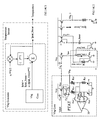
- FIG. 1 is the platform of the green technology which includes the Xtaless clock. Inductorless PMU and PA.
- FIG. 2 is to illustrative the principle of the amplitude controller for the LC resonator: (A) is the differential LC resonator; (B) is the oscillatory curve and the frequency of the output voltages: (C) is the chaos of the chaotic LC resonator; (0) is to vary the amplitude with the amplitude control to keep the output oscillation to be the fixed frequency fo.
- FIG. 3 is the conventional frequency control for the LC resonator;
- (A) is the system of the conventional frequency control:
- (B) is the operating curves of the frequency control for the LC resonator.
- FIG. 4 is to illustrate the parametric capacitors effect and the parametric bulk diode effect on the LC resonator: (A) is the LC resonator having both the parametric capacitors and the parametric bulk diode; (B) is the operation of the parametric bulk diode at the large amplitude; the equivalent capacitor for this parametric bulk diode is large; (C) is operation of the parametric bulk diode at the small amplitude; the equivalent capacitor for this small bulk diode is small: (D) is the signal flow block diagram to show the catastrophic effect of the temperature on the LC resonator.
- FIG. 5 is to illustrate the temperature self-compensation capacitor;
- A) is the MIM capacitor:
- B) is the MOM type capacitor;
- C) is the parallel or serial connection of MIM capacitor and MOM capacitor to have the temperature self-compensation:
- D) is the MIOM capacitor to have the temperature self-compensation:
- E) is the characteristics of versatile capacitors.
- FIG. 6 is to show the innovation of self-compensate bulk diode topology to compensate for the bulk diode capacitance variation in the Varactor Free Amplitude Controlled Oscillator (VFACO) LC oscillation:
- A is the spectrum of the idealized LC resonator;
- B is the spectrum of the LC resonator having the frequency-tuning effect due to the variance of the bulk diode capacitance induced by the voltage-swing of the output voltage:
- C) is the spectrum of the LC resonator having the self-compensation bulk diode capacitance for the voltage swing:
- D) is the differential mode diode having the self-compensation bulk diode capacitance for the voltage swing;
- E is the differential mode NMOS having the self-compensation bulk diode capacitance for the voltage swing:
- F is the differential mode PMOS having the self-compensation bulk diode capacitance for the voltage swing;
- G is the differential mode NMOS
- FIG. 7 is the Varactor Free Amplitude Controlled Oscillator (VFACO) having LC resonator with the amplitude controller:
- A is the Amplitude Controlled Oscillator (ACO) circuit schematic diagram of the amplitude controlling LC resonator:
- B is the operation curve of the Amplitude Controlled Oscillator (ACO) LC resonator with amplitude controller:
- C is the operation characteristics of the parametric bulk diode of the active MOS.
- FIG. 8 is the alternative simplified design of the Amplitude Controlled Oscillator (ACO) LC resonator with amplitude controller:
- FIG. 9 is the conventional LC resonator has the humidity moisture sensitivity and package problem.
- FIG. 10 is the comparison between the LC resonator with the frequency controller and the LC resonator with the amplitude controller;
- A is the Voltage Controlled Oscillator VCO type LCO open-loop free running frequency controller LC resonator:
- B is the Amplitude Controlled Oscillator ACO type LCO closed-loop feedback controlling amplitude controller LC resonator.
- FIG. 11 is the detailed block diagram of the Voltage Controlled Oscillator VCO type LCO open-loop free running frequency controller LC resonator;
- A is the conventional open-loop free running frequency controller LC resonator which only has the parameter setting functions for the free-running LC resonator;
- B the signal flow of the frequency controller is varactor capacitance;
- C is the operation of the open-loop free running frequency controller LC resonator with the frequency-test-curve-fitting methodology to fit for the frequency variation.
- FIG. 12 is the detailed block diagram of the Amplitude Controlled Oscillator ACO type LCO closed-loop feedback controlling amplitude controller LC resonator;
- A shows the amplitude controller having masked out the gain variance due to the aging, temperature and process, etc;
- B the signal flow of the amplitude controller is oscillation amplitude:
- C is the operation of the closed-loop feedback controlling amplitude controller LC resonator.
- FIG. 13 is the non-linear Kvco for the closed-loop feedback controlling amplitude controller LC resonator in PLL:
- (A) is the characteristic curve of the non-linear Kvco:
- (B) is the timing waveform ⁇ t of the PFD in PLL:
- (C) is the implementation of the non-linear Kvco with the timing waveform of the PFD to be the ⁇ f, where the ⁇ f ⁇ t/ ⁇ t.
- FIG. 14 is the low latency controller circuit for the LC resonator with the power management and spread spectrum capabilities;
- A is the circuit block diagram of the low latency controller circuit for the LC resonator with the power management and spread spectrum capabilities;
- B is the operational characteristics curve of the low latency controller circuit for the LC resonator;
- C 1 is the block diagram for the Iptat, Iptat_linear and temperature sensor;
- C 2 is the circuit implementation for the block diagram in FIG. 14 C 1 ;
- D 1 is the block diagram for the Ictat, Ictat_linear, Ibg_linear and Vbg_linear:
- D 2 is the circuit implementation for the block diagram in FIG. 14 D 1 .
- FIG. 15 is the SSEML Scalable Single End Multiple Level PMU Power Management Unit interface: (A) is the protocol of the SSEML: (B) is the interface between the Xtaless ClockChip and the other chip: (C) is the block diagram for the SSEML in the Xtaless ClockChip; (D) is the detailed state transition block diagram for the SSEML in the Xtaless ClockChip: (E) is the operation of the SSEML in the Xtaless ClockChip to reduce the power of LC resonator without changing the clock frequency.
- FIG. 16 is the fast flying-scan calibration/test circuit for LC resonator.
- FIG. 17 is the amplitude controller for the LC resonator: (A) is the circuit schematic of the amplitude controller LC resonator: (B) is the amplitude reference generator; (C) is the common mode generator.
- FIG. 18 is the amplitude controller for the LC resonator with the addition of the bulk diode to compensate the capacitance variance due to the voltage swing.
- the polarity of the bulk diode is reverse of the conventional frequency control type LC resonator.
- FIG. 19 is the alternative design of the amplitude controller for the LC resonator;
- (A) is the circuit schematic of the amplitude controller LC resonator:
- (B) is the maximum reference generator;
- (C) is the minimum reference generator.
- FIG. 20 is the alternative design of the amplitude controller for the LC resonator with the addition of the bulk diode to compensate the capacitance variance due to the voltage swing.
- FIG. 21 is the alternative design of the amplitude controller for the LC resonator with the double gain-boost Q technology.
- FIG. 22 is the alternative max-min type design of the amplitude controller for the LC resonator with the double gain-boost Q technology.
- FIG. 23 is the simplified alternative design of the amplitude controller for the LC resonator with the double gain-boost Q technology.
- FIG. 24 is the amplitude controller for the N type latched amplifier having the inductors as the active load: (A) is the amplitude controller for N type latched amplifier having the coupled planar inductor; (B) is the redraw of the amplitude controller for N type latched amplifier having the magnetic coupled inductor with the programmable supply voltage; (C) is the double gain-boost-Q DGBQ amplitude controller for N type latched amplifier having the coupled planar inductor; (D) is the redraw of the double gain-boost-Q DGBQ amplitude controller for N type latched amplifier having the magnetic coupled inductor with the programmable supply voltage.
- FIG. 25 is the amplitude controller for the P type latched amplifier having the inductors as the active load: (A) is the amplitude controller for P type latched amplifier having the coupled planar inductor; (B) is the redraw of the amplitude controller for P type latched amplifier having the magnetic coupled inductor with the programmable supply voltage; (C) is the double gain-boost-Q DGBQ amplitude controller for P type latched amplifier having the coupled planar inductor: (D) is the redraw of the double gain-boost-Q DGBQ amplitude controller for P type latched amplifier having the magnetic coupled inductor with the programmable supply voltage.
- FIG. 26 (A) is the amplitude controller applying to the source degenerated LC VCO:
- (B) is the amplitude controller applying to the high-frequency LC VCO design using capacitive degeneration.
- FIG. 27 is the amplitude controller applying to the quadratic QVCO; (A) is the amplitude controller applying to the electric coupling quadratic QVCO: (B) is the amplitude controller applying to the magnetic coupling quadratic QVCO.
- FIG. 28 is the amplitude controller applying to the crystal oscillator and the FBAR oscillator:
- A is the section view of voltage-tunable film bulk acoustic resonator (FBAR):
- B is the electric model of the film bulk acoustic resonator (FBAR):
- C is the amplitude controller applying to the crystal oscillator;
- D is the amplitude controller applying to the FBAR oscillator.
- FIG. 29 (A) is the conjugate current mode amplitude controller for the LC resonator; (B) is the conjugate voltage mode amplitude controller for the LC resonator; (C) is the conjugate voltage mode amplitude controller for both power supply and bulk diode control of the LC resonator; (D) is the block diagram of the amplitude controller.
- FIG. 30 is the comparison between the conventional frequency controller LC resonator and our amplitude controller LC resonator: (A) is the open-loop free-running frequency controller; (B) is the closed-loop feedback controlled amplitude controller.
- FIG. 31 is the spread-spectrum amplitude controller LC resonator; (A) is the spread spectrum generator being embedded in the amplitude controller (B) is one kind of the implementation of the spread spectrum generator with the TRNG true random number generator.
- FIG. 32 (A) is the generic constant temperature resonator; (B) is the constant temperature Xtaless resonator: (C) is the constant temperature crystal resonator; (D) the constant temperature LC resonator.
- FIG. 33 (A) is constant temperature MS0-GBQ-AMC-LCO Clock: (B) is the on-chip self-heating temperature compensation calibration system.
- FIG. 34 is the single-chip PMU system for the LCD TV.
- FIG. 35 are the versatile sockets for modern home: (A) is the AC socket and the smoker socket; (B) is the AC socket, the smoker socket and the USB socket.
- FIG. 36 (A) is the circuit schematic for the smart socket and single chip PMU: (B) is the VZS voltage zero switching operation for the smart socket and single chip PMU: (C 1 ) is the unified SMLDVR switch mode and low drop voltage regulator; (C 2 ) is the operation curves in the SMLDVR and idle mode to save the power: (D) is the configurable boost and buck SMPS.
- FIG. 37 is the common mode applying to the envelop extraction recovery EER of power amplifier: (A) is the N type envelop extraction recovery EER of power amplifier; (B) is the P type envelop extraction recovery EER of power amplifier.
- FIG. 38 (A) is planar inductor having the magnet loop being confined in a slice structure; (B) is the planar inductor symbol; (C) is the alternative planar inductor symbol.
- FIG. 39 is the on-chip EMI-Free planar inductor: (A) is the top view of the EMI-Free planar inductor; (B) is the top view of the alternative design of EMI-Free planar inductor: (C) is the section view of the on-chip EMI-Free planar inductor planar inductor: (D) is the alternative different section view of the on-chip of the EMI-Free planar inductor: (E) the another different section view of the on-chip EMI-Free planar inductor: (F) is the soft magnetic material covering over and under the chip; (G) is the magnet covering over and under the whole chip: (H 1 ) is the top view of the EMI-Free spiral-type planar inductor; (H 2 ) is the section view of the EMI-Free spiral-type planar inductor: (I 1 ) is the top view of the EMI-Free solenoid-type planar inductor: (I 2 ) is the section view of the EMI-Free sole
- FIG. 40 is the single integrated LC resonator; (A) is the inductor current flowing to charge up the top plate: (B) is the capacitor charge storage: (C) is the inductor current reverse flowing to charge the bottom plate: (D) is the capacitor reverse charge storage.
- FIG. 41 is the dual integrated LC resonator; (A) is the inductor current flowing to charge up the top plate; (B) is the capacitor charge storage; (C) is the inductor current reverse flowing to charge the bottom plate: (D) is the capacitor reverse charge storage.
- FIG. 42 is the PCB version on-board planar inductor;
- A) is the section view of the embedded-in on-board planar inductor;
- B) is the three dimensional 3-D view of the on-board planar inductor;
- C) is three-dimensional view of the current loop for the on-board planar inductor.
- FIG. 43 is the electric static discharge switch ESDS-PCB having the power and ground layer closing to the top and bottom layers:
- (A) is the section view of ESDS-PCB:
- (B) is the equivalent schematics of the ESDS-PCB:
- (C) is the section view of ESDS-PCB during the ESD;
- (D) is the equivalent schematics of the ESDS-PCB during the ESD.
- FIG. 44 is the ESDS-PCB having the power and ground layer at the middle of the layers with the buried vias for high-speed high-frequency and RF circuits;
- A is the section view of ESDS-PCB:
- B is the equivalent schematics of the ESDS-PCB;
- C is the section view of ESDS-PCB during the ESD;
- D is the equivalent schematics of the ESDS-PCB during the ESD.
- FIG. 45 is the ESDS-PCB having the power and ground layer at the middle of the layers with the contacting vias for low-speed low-frequency circuits;
- (A) is the section view of ESDS-PCB:
- (B) is the equivalent schematics of the ESDS-PCB:
- (C) is the section view of ESDS-PCB during the ESD:
- (D) is the equivalent schematics of the ESDS-PCB during the ESD.
- FIG. 46 is the illustrated example of the two-dimensional 2-D placement and via assignment for ESDS IC, hybrid PCB and high acceleration high-g PCB, etc;
- (A) is the section view of the high-g PCB;
- (B) is the generic placement and route for the ESDS IC, hybrid PCB and high-g PCB, etc.
- FIG. 47 is the 2-D placement and via assignment for ESDS IC, hybrid PCB and high-g PCB, etc for the switch box:
- (A) is the switch box;
- (B) is the circular topology of the switch box as shown in FIG. 47A :
- (C) is the boundary-split of the switch box;
- (D) is the linear placement for the switch box:
- (E) illustrates the “Tangs Theorem”: for N 2-pin nets; there are at most (N ⁇ 2) vias.
- FIG. 48 is to illustrate the minimum-via maximum planarization algorithm; (A) building up the linear interval graph and calculates the “Tangs Distance” for the linear interval graph: (B) removing the net having the maximum “Tangs Distance” and update the “Tangs Distance” for the linear interval graph: (C) removing the net having the maximum “Tangs Distance” and update the “Tangs Distance” for the linear interval graph: (D) applying the “Tangs Theorem” to remove one via at the beginning and end of this linear graph; (E) is the final optimum via assignment for the switch box router.
- FIG. 49 is to show the merge and remove of the 2-pin nets in the linear placement algorithms for the maximum planarization: (A) two successive pins belong to the same net can be merged: (B) the merged net is removed front the linear placement interval graph.
- FIG. 50 is to show how to modify the multiple-pin nets to be multiple 2-pin net; (A) is the multiple-pin net: (B) with the pin-splitting, the multiple-pin net is split to be 2-pin nets.
- FIG. 51 is the 2-D placement problem for the global via assignment with the maximum planarization
- FIG. 52 is the 2-D placement problem for the global via assignment with the maximum planarization and the boundary pin assignment.
- FIG. 53 (A) is one kind of split for the boundary to convert the 2-D placement to be the circular linear placement problem: (B) is the corresponding circular linear placement to the 2-D placement as shown in FIG. 51A .
- FIG. 54 (A) is the another kind of split of the boundary to convert the 2-D placement to be the circular linear placement problem: (B) is the corresponding circular linear placement to the 2-D placement as shown in FIG. 52 ; building up the linear interval graph and calculates the “Tangs Distance” for the linear interval graph: (C) is the alternative representation of the circular linear interval graph; (D) making the detour routine for the net having the maximum “Tangs Distance”; (E) is the optimum 2-D maximum planarization and minimum via assignment.
- FIG. 55 is the flow chart for the optimum via assignment for maximum planarization and minimum via assignment.
- FIG. 56 is the Xtaless ClockChip: (A) is the signal flow block diagram of the Xtaless ClockChip; (B) is the floor Planning and Layout of the Xtaless ClockChip.
- FIG. 57 (A) is the Xtaless ClockChip including the PLL which can serve as IP of RadioChip.
- SerDesChip, etc: (B) is the Xtaless ClockChip using the frequency divider to replace the PLL to generate the clock.
- FIG. 58 is the Super-Speed Synchronization Global Lock Loop 3SGLL for the USB-3 with the Xtaless ClockChip green technology:
- A is the hierarchical frequency layer and the phase layer of 3SGLL USB-3:
- B is the late and early CDR sampling;
- C is the circuit implementation of the late and early signal:
- D is generic 3SGLL USB-3 having the DLL, PLL and the Xtaless Clock;
- E is the PD for Phase Loop and Early/Late for Frequency Loop with the GBQ LCO as the high frequency Xtaless Clock.
- FIG. 59 is the Green Safety Chip design for the tire safety with the Xtaless ClockChip green technology: (A) is the tire having the tire-pressure monitor; (B) is the tire-pressure monitor mounted on the stub: (C) is the block diagram of the tire-pressure monitor.
- Green Technology is very challenge. Shrinking the device size means both the save of the resource and energy. As shown in FIG. 1 , the thick dark lines enclosed components are the key components of the green technology.
- the Xtaless clock and Inductorless PMA and PA are the backbone of the green technology platform.
- MS0 is the Moisture Sensitivity zero.
- the clock frequency is independent of the moisture level.
- GBQ is the Gain-Boost-Q.
- the AMC is the closed-loop feedback controlled Amplitude Controller.
- the Xtaless clockchip will take over all the clock and frequency control market. From the design methodology and system perspective, the amplitude controller is completely different from the conventional frequency controller of the prior-arts.
- the LC resonator In the undergraduate school basic circuit theory, the LC resonator is treated as the linear circuit to be “periodic circuit”.
- the frequency controller of all the prior art is derived from the linear circuit theory. They use the set & go, open-loop free-running LC resonator approach. They set the parameters for the LC resonators first, then let the LC resonator free to run. In summary, the frequency controller of the prior art is the open-loop free-running methodology for the linear periodic LC resonator circuit.
- the amplitude controller of our innovation is the closed-loop feedback/feedforward-controller methodology for the nonlinear chaotic LC resonator circuit.
- the traditional frequency controller of the prior art is based on the wrong design methodology. Actually, there should not have the frequency controller at all. As shown in FIG. 2A , it is a LC resonator.
- the traditional approach is based on the free-running concept. There is the implicit “no-touch” concept on the LC resonator. Let the LC resonator to be free-running mode. Any control on the LC resonator will interrupt the natural frequency oscillation of the LC resonator. Therefore, set the supply current and set the inductance L and capacitance C, then let the LC resonator go. So, it is the frequency setting, not the frequency controlling.
- the amplitude of the output voltage of the LC resonator is varying and the frequency is varying accordingly.
- FIG. 2C on the phase plot of the LC resonator, it shows that the free-running naturally resonant LC resonator is a chaotic circuit, not a periodic circuit.
- the conventional thinking of the LC resonator is a periodic circuit is completely wrong.
- the chaotic degree is very small that all the people think the LC resonator is a periodic circuit and uses the free-running approach. For the free running mode, it just needs to set the correct L and C value and let it go. It is the frequency setting, not frequency control. This is valid only for the ideal passive resonator having no active devices.
- the fundamental philosophy of the amplitude control is to recognize the LC resonator is a low-degree chaotic circuit. We need to develop the anti-chaotic circuit to get rid of the chaos of the LC resonator. Furthermore, as shown in FIG. 2D , it shows the frequency being the function of the amplitude. In other words, controlling the amplitude to be a fixed value, we can fix the resonant frequency at a constant frequency. This is the fundamental concept of the amplitude control for real-life active resonator.
- V is the amplitude of the LC resonator.
- the Amplitude Controller is a system and architecture level LC resonator design.
- the three levels technology breakthrough innovations as follows.
- FIG. 3A it is the conventional frequency controller LC resonator in the prior an. It is noted that the polarity of the varactor is completely wrong due to the failure of the Xtaless ClockChip problem. It makes the clock spectrum spreading due to the voltage swing of the oscillation.
- FIG. 3B at the temperature T 0 , the LC resonator is oscillates at fo frequency with amplitude A 0 . As the temperature varies front T 0 to T 1 , the frequency increases to bell. To slow down the LC resonator from f 1 to f 0 , the control voltage Vctrl is changed to add more capacitance to the LC resonator.
- the on-chip temperature sensor TEMP sends the temperature information to ADC. Then the corresponding control voltage information stored in the non-volatile memory and register NVM REG is taken out and sent to DAC to convert to be the analog Vctrl signal to adjust the capacitance variance of the LC resonator.
- the control voltage Vctrl changes to tune the average capacitance to adapt to the variance of the capacitance due to the temperature.
- the amplitude-control clock chip is the only clock chip which works for the RF/Wireless product. It doesn't use frequency control varactor that it will not generate the Close To Carrier CTC phase. Furthermore, the Gain-Boost-Q (GBQ) amplitude K common-mode control will increase the Q of the LC resonator a lot that any CTC phase noise will be further suppressed with the GBQ amplitude control.
- GBQ Gain-Boost-Q
- the fine tune of the oscillatory frequency is done with the amplitude without the varactor diode. There is no CTC phase noise generation. On the contrary, the Gain-Boost-Q amplitude control further suppress the other CTC phase noise.
- the amplitude control is not only not generating CTC phase noise but also increasing Q to suppress the other CTC phase noise. Therefore, the amplitude control clock chip is the only clock chip which can use in the RF/Wireless/Cellular Phone products.
- FIG. 4 shows how the temperature induces the catastrophic effect on the oscillation frequency of the LC resonator.
- the equivalent capacitance of the parametric varactor diode of MOS devices is large.
- the equivalent capacitance of the parametric varactor diode of MOS devices is small.
- the catastrophic frequency variance due to the temperature variation is as shown in FIG. 4D .
- the parametric capacitance Cp 1 , Cp 2 , Cn 1 , Cn 2 of the LC resonator decreases.
- the resonant frequency of the LC resonator increases and the resonant amplitude decreases as shown in FIG. 3B .
- FIG. 3B As shown in FIG.
- the equivalent capacitance of the bulk diode of the MOS devices Mp 1 , Mp 2 , Mn 1 and Mn 2 are reduced further.
- FIG. 4D it becomes a catastrophic unstable loop.
- the catastrophic phenomenon is the frequency higher, the less parametric capacitor; the less parametric capacitor, the frequency higher, etc. Therefore, even with the tiny temperature variation, the catastrophic unstable loop will make the very large capacitance variance. Therefore, with the amplitude controller, we can break the catastrophic unstable loop.
- the amplitude controller controls the bulk connections of the MOS devices Mp 1 , Mp 2 , Mn 1 and Mn 2 .
- the bulk nodes of the gm-amplifier is controlled by the output of the amplitude controller.
- a Green Technology Platform apparatus comprises a magnetic-electric resonator accommodating to generate a plurality of clock signals having a resonant frequency.
- a gm-amplifier is coupled to the magnetic-electric resonator and an oscillator controller is coupled to the magnetic-electric resonator and gm-amplifier means.
- the oscillator controller is adapted to generate a plurality of outputs to control a plurality of bulk nodes of the gm-amplifier. Furthermore, a plurality of outputs are correlated with temperature.
- the LCO has the capacitor bank for the set of the coarse frequency and the LCO uses the varactor diode bank for the fine tune of the capacitor to compensate the temperature variance.
- the frequency controller is an isolated controller.
- the frequency controller sends the varactor diode controlling bits to switch on or off the varactor diode of the LCO.
- the LCO is free-running. There is no feedback control for the frequency control.
- the amplitude controller sends the amplitude control bits to the amplitude control register and send the common-mode control bit to the common-mode control register.
- the amplitude DAC will convert the amplitude control bits to the amplitude voltage; the common-mode DAC will convert the common-mode control bits to the common-mode voltage.
- the amplitude control feedback control amplifier and common-mode feedback control amplifier make the comparisons between the LCO amplitude and common-mode voltage to set the LCO to oscillate at the specified amplitude to have the specified frequency to compensate the capacitance variance due to the temperature variance.
- the amplitude control is very complicate feedback control loop.
- the frequency control of the LCO is very simple isolated controller having the open-loop free-running oscillation.
- the frequency control can be completely decoupled from the LCO resonator.
- the frequency controller doesn't include the LCO model.
- the amplitude control of the LCO is very complicated coupling controller having the closed-loop feedback controlled oscillation.
- the amplitude control cannot be decoupled from the LCO resonator. So, in the drawing, the amplitude controller does include the LCO model to illustrate the closed-loop feedback amplitude controlling relations.
- the interdigital fringe-capacitance MOM capacitor has the positive temperature coefficient TC.
- the MIM capacitor has the negative temperature coefficient TC.
- the temperature increase the distance between the plates increases that the capacitance decreases.
- FIG. 5C as the MIM and MOM connected in parallel or in series, the temperature increases effect of MIM and MOM will cancel with each other.
- FIG. 5D the MIOM has the hybrid structure of the MIM and MOM that the it has the temperature self-compensation effect. Both FIG. 5C and FIG. 5D are referred to the temperature self-compensation capacitor.
- FIG. 6 is to show the innovation of Varactor Free Amplitude Controlled Oscillator (VFACO) self-compensate varactor topology to compensate for frequency shift due to the bulk capacitance variation in the Varactor Free Amplitude Controlled Oscillator (VFACO) LC oscillation.
- VFACO Varactor Free Amplitude Controlled Oscillator
- FIG. 6A the spectrum of the idealized LC resonator is a ⁇ function at frequency fo.
- the frequency fo is only the weighted average of the capacitor.
- the variance of the capacitance of the bulk diode causes the fine modulation of the frequency. Even worse, the variance of the capacitance of bulk diode is anti-symmetric.
- one side of varactor is more forward bias and the junction capacitance increases. On the other side is more reverse biased and the junction capacitance decreases, and vice versa. Therefore, the capacitor loading at the two node Vo+ and Vo ⁇ are not the same and varies. Therefore, the oscillation curve is distorted and the frequency drifts. To eliminate the frequency drift.
- FIG. 6C is the spectrum of the LC resonator having the self-compensation bulk diode capacitance for the voltage swing.
- FIG. 6D is the differential mode diode having the self-compensation varactor capacitance for the voltage swing.
- FIG. 6E is the differential mode NMOS having the self-compensation varactor capacitance for the voltage swing.
- FIG. 6F is the differential mode PMOS having the self-compensation varactor capacitance for the voltage swing.
- FIG. 6G is the differential mode NMOS and PMOS having the self-compensation bulk diode capacitance for the voltage swing. Referring to FIG. 4A , as shown in FIG. 6H , it is compensating bulk diodes to compensate the bulk diodes of NMOS devices Mn 1 , Mn 2 and PMOS devices Mp 1 , Mp 2 .
- FIG. 4A is compensating bulk diodes to compensate the bulk diodes of NMOS devices Mn 1 , Mn 2 and PMOS devices Mp 1 , Mp 2 .
- FIG. 4A is compensating bulk diodes to compensate the bulk diodes of NMOS devices
- FIG. 6H is the bulk diode Compensation for the self-compensation bulk diode capacitance for the voltage swing.
- the self-compensation bulk diode in FIG. 6H and the NMOS devices Mn 1 , Mn 2 and PMOS devices Mp 1 , Mp 2 are corresponding to the self-compensation bulk diode capacitance as shown in FIG. 6G .
- the polarity of the NMOS devices Mn 1 , Mn 2 and PMOS devices Mp 1 , Mp 2 just reverse the conventional connections of the prior art. In other words, the connections of the prior art are wrong.
- the prior art fails to recognize the voltage swing induced frequency shift problem.
- the wrong connection of the polarity for the prior art varactor diode made the case even worse.
- to be the trimless/trimfree LC resonator for the Xtaless ClockChip it needs following four techniques.
- the amplitude control we use the active NMOS devices Mn 1 , Mn 2 and PMOS devices Mp 1 , Mp 2 as the bulk diode directly. We don't need the extra varactor diode as the prior art does. Furthermore, for the differential bulk diode and differential diode as shown in FIG. 6 , the amplitude reference is related to temperature. LCO has the amplitude and common mode voltage controlled by the amplitude controller to compensate the temperature variation of the LCO.
- the self-compensation bulk diode in FIG. 6 has both the voltage compensation and temperature compensation effects.
- the compensate bulk diodes are the sum of the active device and the buffer.
- the bulk of the buffer is biased by the control voltages ctrlp and ctrln, too.
- the N-type latched amplifier as shown in FIG. 24A there is no PMOS active device needed to compensate.
- the P-type latched amplifier as shown in FIG. 25A there is no NMOS active device needed to compensate.
- Varactor Free Amplitude Controlled Oscillator (VFACO) amplitude controller has several applications in the control of the LC resonator.
- VFACO Varactor Free Amplitude Controlled Oscillator
- the varactor diode of the prior art is added to compensate the capacitance variance due to the catastrophic unstable loop. There is no need for the additional varactor diode at all.
- the addition of the varactor diode comes from the VCO of the PLL.
- the VCO of the Xtaless ClockChip is not the VCO of PLL. It is wrong to take the VCO of the PLL design to the VCO of the Xtaless ClockChip without the knowledge of the difference of the VCO of the PLL and the VCO of the Xtaless ClockChip.
- the MOS devices Mp 1 , Mp 2 , Mn 1 and Mn 2 can serve as the bulk diode. We don't need the extra varactor diode at all.
- Varactor Free Amplitude Controlled Oscillator (VFACO) amplitude controller LC resonator has the 1 st order self-compensation to have the self-adaptive capabilities to the variance of the environment.
- the trimming or calibration is only for the 2 nd order effect. All the 1 st effect has been cancelled in the 1 st order self-compensation and self-adaptive process of the amplitude controller LC resonator. Therefore, as we design the Varactor Free Amplitude Controlled Oscillator (VFACO) LC resonator, we need to design for the 1 st order self-compensation with the amplitude controller. Then use the trimming to correct the 2 nd order effect. A lot of times, the 2 nd order is so minor that it is no need to trimming. It is the trimming-free Xtaless ClockChip.
- the design Target/Object Oriented is Self-Adaptive to cancel all the 1 st order effects.
- the order self-compensation design techniques for the amplitude controller LC resonator are as follows.
- the increment of the inductor length is ⁇ T. Therefore, the decrease of current is proportional to ⁇ T.
- This capacitor temperature effect ( ⁇ C/C) ⁇ ( ⁇ T/T) is applied to both the MOS capacitor and the main capacitance C.
- the inductor and capacitor has the LC Self-compensation effect as follows.
- Varactor Free Amplitude Controlled Oscillator (VFACO) LC amplitude Controller.
- Vpeak and Vvalley are the really measurements of the peak value and valley value of the V+ and V ⁇ . It conies from the feedback control. There are many ways to control the Vamp and Vcom. However, their principles are based on the same amplitude controller principle. Vamp and Vcom. No matter which ways the circuit designs are, there is the need to control both Vamp and %/coin at the same time with the versatile ways.
- FIG. 7A shows the way Varactor Free Amplitude Controlled Oscillator (VFACO) to control vcom and gcom to control the Vmax and Vmin. Controlling Vmax and Vmin, then we can control the Vamp and Vcom.
- the control voltages ctrlp, ctrln tries to follow the voltage vcom and gcom to have the proper control voltage conditions for the bulk diode.
- the bulk control voltage ctrlp is connected to the PMOS bulk node 999 and the bulk control voltage ctrln is connected to the NMOS bulk node 888 . However, it might make the minor modification for the 2 nd order effect to cancelling the 2 nd order variance of the oscillation conditions. As shown in FIG.
- FIG. 7B is the alternative design of the Varactor Free Amplitude Controlled Oscillator (VFACO) amplitude controller LC resonator.
- VFACO Varactor Free Amplitude Controlled Oscillator
- the conventional frequency controller of the prior art never mentions how to handle the variance of the humidity on the moisture sensitivity level.
- they just used the ceramic package to walk around the short term test problem.
- the plastic package has the short transient time.
- the prior art uses the ceramic package having the long-term transient constant to walk the test problem.
- the ceramic package cannot test the change of the frequency.
- the moisture sensitivity problem still comes out. It is the most serious problem of the prior art of the Xtaless ClockChip.
- the signal flow block diagrams show the difference between the conventional frequency controller and the amplitude controller.
- FIG. 10A it is the open-loop frequency controller. It just the set & go for the oscillation frequency. In the real life application, there is no other reference clock. There is no feedback for the frequency deviation in the real time. Therefore, it is the open-loop without any control.
- FIG. 10B the Closed Loop Amplitude Control has the oscillation amplitude deviation to be the feedback control. Controlling the amplitude, we can have the fixed oscillation frequency for the LC oscillator. It is the closed-loop feedback control.
- FIG. 11A it is the block diagram for the conventional frequency controller. As shown in the dark blocks, the process, temperature and aging, etc, cause the gain change, capacitance change and induce the amplitude change, frequency change of the LC resonator.
- FIG. 11B is the signal flow for the conventional frequency controller for the temperature variation case. As the temperature varies, the temperature sensor senses the variance and sends the data through ADC to NVM to load the varactor control voltage data into the Varactor register. The DAC converts the Varactor register data to the varactor control voltage V ctrl to control the capacitance of the varactor diode to vary the capacitance of the LC resonator to tune up the LC resonator to be the fixed voltage.
- the temperature increases from T 0 to T 1 and the frequency increases to be f l and the amplitude decreases to be A 1 .
- the LC resonator will oscillate at the frequency f o with amplitude A 1 .
- the variance amplitude will change the resonance of the LC resonator.
- the variance amplitude changes the equivalent capacitance of the LC resonator.
- the mutual influence of the amplitude and the capacitance of the LC resonator make the trimming of the frequency control become intractable. Furthermore, this process has to repeat for all the parameters.
- the MSL0-GBQ-AMC Xtaless ClockChip not only has the electric amplitude controller but also has the magnetic confinement.
- the frequency controller generates the control voltage and varactor capacitance variance for the LC resonator; the amplitude controller generates the specified amplitude for the LC resonator.
- FIG. 12B it has the option to be the analog temperature sensor without ADC.
- FIG. 12C as the temperature increase from T 0 to T 1 , the capacitance decreases and the frequency increases from fo to fl. Adjusting the amplitude according to the specified amplitude A 1 , the LC resonator will oscillates at the resonant frequency f o .
- the control variable of the amplitude controller is completely different from the control variable of the frequency controller.
- the amplitude controller has the capability to self-adaptive to self-compensate for the gain change and capacitance change with the closed-loop feedback control. All the process, temperature and aging, etc will be convert to the gain-change and capacitance change. In other words, the amplitude and common mode controller has the self-adaptive capability to self-compensate for the process, temperature and aging, etc change. At least, the amplitude and common mode controller has the 1 st order compensation for the process, temperature and aging, etc change. Therefore, the trimming for the amplitude controller only for the 2 nd order minor effects.
- the phase lock loop PLL For the Xtaless ClockChip, there is an option to use the phase lock loop PLL to boost the frequency (1 GHz) to high frequency (80 GHz).
- the VCO of the clock reference should not have the varactor diode to tune the frequency.
- the VCO of the PLL has the voltage control Vctrl to tune the oscillation frequency.
- the high frequency PLL as shown in FIG. 13A , the nonlinear Kvco is used.
- the nonlinear Kvco has both large lock range and is jitterless at the locking frequency f o . Only the nonlinear Kvco can have both characteristics. As the deviation of frequency is large, the Kvco is large: as the deviation of frequency is small, the Kvco is small.
- FIG. 13C One implementation of the nonlinear Kvco is shown as FIG. 13C .
- the larger the frequency deviation is the larger capacitance is connected to V ctrl lpf and the smaller capacitance is connected to V ctrl avg .
- the smaller the frequency deviation is the smaller capacitance is connected to V ctrl lpf and the larger capacitance is connected to V ctrl — avg .
- the frequency deviation is approximated with of ⁇ f ⁇ 1/ ⁇ t where the ⁇ t as shown in FIG. 13B .
- ⁇ t is the period between the two successive edge of the reference clock and the feedback clock.
- the T2B time-to-binary, converts the ⁇ t to the binary value to switch the mux to have the nonlinear Kvco.
- the rising curves for the Vbg and Ibg have the different slopes.
- the V bg — OK generates the V bg — OK step function as the Vbg signal is ready.
- the V bg OK is to switch off the initial power supply for the LCO resonator.
- the LC resonator uses the current source I start to generate the clock immediately as the power is on.
- the power supply is automatically in the normal amplitude controller operation.
- the I start switch can be turned off slowly and the Amplitude Controller will take over all the power supply work.
- the Vbg bg — OK signal will turn on the I start switch that the LC resonator still can work to have all the system shut down according the power-down sequence.
- the bandgap module and temperature sensor share the same circuits.
- the temperature sensor has much higher linear requirement than the bandgap reference voltage requirement.
- the V bg and I bg are nonlinear and need to have the curvature compensation. It needs to eliminate the squared terms I ptat 2 and I ctat 2 from the I ptat and I ctat to be I ptat — linear and I ctat linear .
- the Xtaless ClockChip uses the temperature sensor to calibrate the frequency. The nonlinearity of the temperature sensor will add to the nonlinearity of the frequency over the temperature.
- the nonlinearity of the temperature sensor is derived from the I ptat of the bandgap reference.
- the essential characteristics of the nonlinearity of the I ptat is to we need to make the curvature compensation for the nonlinearity of the V BE of the bipolar device.
- the temperature sensor uses the Proportional To Absolute Temperature I ptat — linear to generate the temperature to have the temperature accuracy of 0.1 degree.
- the I ptat — linear is converted to the biasing voltage (I ptat — linear *pR+V th — n ).
- the power and clock P&C management there is the spread spectrum and the power and clock management to control the oscillation frequency of the LC resonator. As the power saving mode and the clock needs to slow down, the resonant frequency of the LC resonator is reduced.
- the Xtaless Clock Chip there is two ways to make the P&C management. One way is to use the 1 2 C bus and the other way is to use the Clock pin. In case the other chip or system doesn't have the I 2 C bus, the only way is to use the Xtaless Chip clock pin. As shown in FIG. 15 is the power and clock P&C protocol, system and circuit design for the power and clock P&C management with the Scalable Single End Multiple Level PMU.
- FIG. 15A it is our novel innovation of the Scalable Single End Multiple Level P&C protocol. It can support any kinds chip interface with the clock interface.
- the Xtaless Clock chip there is only the power pin, ground pin and clock pin.
- the interface is compatible with the existed 2-pin crystal oscillator which has the XI and XO two pins.
- the Xtaless clock pin is connected with the XO pin of the traditional crystal clock. There is no need to add the extra pin to the Xtaless Clock chip just for the traditional crystal clock power management interface.
- the other chip just needs to pull down or pull up the clock pin, then the Xtaless Chip can detect the pull-down and pull-up to change the P&C status.
- the P&G management there are the normal, doze, standby, suspend, etc state.
- the CLKO there are three states, tri-state, pull up and pull down. As the CLKO input of the other chip is in the tri-state, the P&G state stays in the original state. As the CLKO input of the other chip is in the pull down state, the P&G state moves down one state: as the CLKO input of the other chip is in the pull up state, the P&G state moves up one state, or vice versa.
- the P&C state can change from the normal to doze, standby, suspend, etc state. In other words, as the clock pin is pulled up, the P&C state can chance from the suspend, standby, doze, to etc states back to normal state.
- the state transition can be in sequence or in one-time of bi-state operation if the pull-up or pull-down is held for many clock cycles.
- FIG. 15C shows the detailed signal flow block diagram for the P&C management.
- This P&C management can be applied to any kind resonator.
- the single direction clock signal pin CLKO is served as the bi-directional signal net in the P&C management.
- the other chip pulls up or pulls down the CLKO net, the voltage level, slew rate of the clock edge and the duty cycle will vary.
- the P&C Clock Sensor detects any variance of the voltage level, slew rate of the clock edge or the ditty cycle, it can determine it is tri-state, pull-up state or pull-down state.
- the state transition will transfer to the P&C control. After several cycles, if the state does not come back to the tri-state, then it is presume that this is the bi-state operation or just issues another same state transition command to move state continuously.
- the P&C Controller As shown in FIG. 15D , as the P&C controller receives the state transition command, the P&C Controller identify the correct P&G state memory in the NVM memory to load into the amplitude controller AC Register.
- the amplitude controller issues the amplitude controlling, bulk diode and capacitance controlling commands to the resonator.
- the amplitude controller issues the amplitude controlling commands to control the vcom and gcom of the LC resonator; the amplitude controller issues the bulk diode or capacitance controlling commands to control the ctrlp, ctrln to control the capacitance of LC resonator.
- FIG. 16 shows the fast calibration for the LC resonator.
- the LC resonator is compared with the CLK_ref.
- the initial value is loaded into the register.
- start the counter As the counter difference is large than 2, the counter is reset and the register value is increases or decreases depending on which counter has the larger value.
- the counter value is larger than a large value, say 1000, the test is passed and the register value is stored back to the non-volatile memory NVM.
- the principle and the essential characteristics of the amplitude controller are the amplitude control and the common mode control. However, there are versatile implementations of the amplitude controller. As shown in FIG. 17 , it is the conjugate current mode amplitude controller. The conjugate pairs of the amplitude controller V apo Generator controls the sourcing current and the common mode controller V cmo Generator controls the sinking current, or the vice versa. As shown in FIG. 17B , the V ref.apo Gen is made of the V ref.apo Reg and the DAC. The DAC converts the digital value of the V ref.apo stored in the V ref.apo Reg to be the analog signal V refapo . As shown in FIG. 17C , the V ref.cmo Gen is made of the V ref.cmo Reg and the DAC.
- the DAC converts the digital value of the V refcmo stored in the V ref.cmo Reg to be the analog signal V refcmo .
- the most general V ref.apo Reg value is the temperature compensation of the V ref.apo TempReg.
- the most general V ref.cmo Reg value is the temperature compensation of the V ref.cmo TempReg. As the temperature varies, the V ref.apo TempReg and V ref.cmo TempReg are updated and the new values are loaded from the NVM into the registers to update the reference voltages V refapo and V ref.cmo .
- FIG. 18 is the addition of the bulk diode for the Xtaless Clock Chip voltage swing capacitance self-compensation. It also can add the extra pair of tunable capacitance in FIG. 6 for the LC resonator of the PLL type VCO.
- the V ref.max Gen is made of the V ref.max Reg and the DAC.
- the DAC converts the digital value of the V ref.max stored in the V ref.max Reg to be the analog signal V refmax .
- the V ref.min Gen is made of the V ref.min Reg and the DAC.
- the DAC converts the digital value of the V refmin stored in the V ref.min Ret; to be the analog signal V refmin .
- V ref.max Reg value is the temperature compensation of the V ref.max TempReg.
- V ref.min Reg value is the temperature compensation of the V ref.min TempReg.
- FIG. 20 is the addition of the bulk diode for the Xtaless Clock Chip voltage swing capacitance self-compensation. It also can add the extra pair of tunable capacitance in FIG. 6 for the LC resonator of the PLL type VCO.
- FIG. 21 is the amplitude controller has both the amplitude controller function and the glitch eliminating function for the common voltage source nodes of vcom and gcom.
- the outputs of Vo+ and V ⁇ have nearly perfect sinusoidal output.
- the Q of the LC resonator is much higher than the original amplitude controller circuit as shown in FIG. 17 .
- FIG. 22 shows the alternative design of the double gain-boost-Q DGBQ circuit.
- the amplitude controller function is implemented with the V max and V min .
- FIG. 24 and FIG. 25 show the amplitude controller being the hybrid of feedback and feed forward combination.
- FIG. 24A is the N-type feedback amplitude control and feed forward/local feedback common mode control. It shows the inductor being implemented with the planar MS0 inductor.
- FIG. 24B is redrawn of the FIG. 24A with the latched amplifier having the inductor load. It shows the inductor being implemented with the planar MS0 inductor.
- FIG. 25A is the P-type feedback amplitude control and feed forward/local feedback common mode control. It shows the inductor being implemented with the planar MS0 inductor.
- FIG. 25B is redrawn of the FIG. 25A with the latched amplifier having the inductor load. The inductor is implemented with the planar MS0 inductor, too.
- the feedforward common mode control will destroy the high Q of the GBQ LC resonator.
- the common mode serves as both the power supply and the common mode.
- the injection current of the common mode will generate the glitch to destroy the high Q of the GBQ LC resonator performance.
- FIG. 24C is the DBGQ version of FIG. 24A .
- FIG. 24D is the DBGQ version of FIG. 24B .
- FIG. 25C is the DBGQ version of FIG. 25A .
- FIG. 25D is the DBGQ version of FIG. 25B .
- FIG. 25D is a fully integrated full PMOS Low-Phase-Noise LC VCO. It can run 5 GHz. Now, there is the conjugate push-pull dual-loop control of the amplitude control and common mode control again.
- the Double Gain-Boost-Q DGBQ amplitude controller has the conjugate push-pull dual-loop control of the amplitude control and common mode control. Just you cannot cut one arm to be the single-arm man, there is no way to use the feedforward common mode to walk around the high performance DBGQ conjugate push-pull dual-loop control. Even with the feedforward/local feedback common control, it is still the amplitude controller having both the common mode control and amplitude control. It still does not walk around the amplitude controller problems. However, the performance become even worse.
- FIG. 26A is the amplitude controller applying to the source degenerated LC VCO. It can run 25 GHz.
- FIG. 26B is the amplitude controller applying to the high-frequency LC VCO design using emitter degenerated capacitive degeneration.
- FIG. 27 is the amplitude controller applying to the quadratic QVCO.
- quadratic QVCO There are two kinds of quadratic QVCO: 1) the electric coupling: 2) the magnetic coupling.
- For the electric coupling there are three types of QVCO, a) P-QVCO: TS-QVCO: c) BS-QVCO.
- FIG. 27A is the schematic views of the amplitude controller applying to the electric coupling quadratic P-QVCO with parallel coupling transistors.
- TS-QVCO is the coupling transistor is at the top of the latched NMOS.
- BS-QVCO is the coupling transistor is at the bottom of the latched NMOS. There have the same electric coupling mechanism.
- a Green Technology Platform apparatus comprises an on-chip LC or magnetic-electric resonator.
- the LC or magnetic-electric resonator comprising a inductor or magnetic means and capacitor.
- the inductor or magnetic means has its magnetic field flux being guided by a plurality of soft magnetic material layers.
- the magnetic field flux can be the center of magnet.
- the center magnetic field flux can be the toroid magnetic or planar inductor.
- FIG. 28 is the amplitude controller applying to the crystal oscillator and the FBAR oscillator.
- FIG. 28A is the section view of voltage-tunable film bulk acoustic resonator (FBAR).
- FIG. 28B is the electric model of the film bulk acoustic resonator (FBAR).
- the FBAR has the similar electrical model as the crystal. Both of them are equivalent to the inductor.
- FIG. 28C the amplitude controller applying to the crystal oscillator.
- FIG. 28D the amplitude controller applying to the FBAR oscillator. It is the on-chip voltage-tunable film bulk acoustic resonator FBAR VCO.
- FIG. 29 shows the most advanced amplitude controller in the high-level block diagrams.
- FIG. 29A is the gain-boost-Q GBQ LC resonator has the amplitude controller controlling the conjugate current sources.
- the amplitude controlling signal apo controls the sourcing current and the common mode controlling signal trio controls the sinking current.
- FIG. 29B shows the ultra-high performance double-gain-boost-Q DGBQ LC resonator.
- the voltage sources vcom and gcom are supplied to the LC resonator.
- the Differential Amp has the de-glitch effect.
- the Vcmo provides the common mode information to the Differential Amp to set the common mode of the vcom and gcom.
- FIG. 29A is the gain-boost-Q GBQ LC resonator has the amplitude controller controlling the conjugate current sources.
- the amplitude controlling signal apo controls the sourcing current
- the common mode controlling signal trio controls the sinking
- 29C is the ultra-high performance double-gain-boost-Q DGBQ LC resonator having the MOS devices to serve as the bulk diode, too.
- the ctrlp controls the bulk bias of the NMOS: the ctrln controls the bulk bias voltage of the NMOS.
- the temperature induced capacitance variance of the MOS devices is self-compensated with the biasing controlling voltages ctrlp and ctrln.
- FIG. 30 shows the difference between the conventional frequency controller and our amplitude controller. As shown in FIG. 30A , it is the frequency controller LC resonator.
- the characteristics of the frequency control are the (1) current mode power supply: (2) using the varactor capacitance Cv(T) to compensate the temperature induced the catastrophic frequency variation due to the MOS devices; (3) has to compensate the 1 st order large temperature variation; (4) is the set & go type open-loop free running.
- the temperature sensor is to adjust the varactor diode controlling voltage to change the Cv(T) capacitance directly. It is an open loop set & go system. There is no close loop feedback and no check for the supply current, etc. Everything is set and go. Even the prior art adopts the part of GBQ technology derived from our amplitude controller, however, it still doesn't use the variance of the amplitude to control the variance of the frequency. It still uses the varactor diode to vary the frequency. As shown in FIG. 6B , the spectrum spreading of the oscillation is due to the voltage swing inducing the variance of bulk capacitance and varactor capacitance to have the self-modulation change the frequency.
- FIG. 30B shows the amplitude controller LC resonator.
- a Green Technology Platform apparatus comprises a reference resonator adapted to provide the reference signal having a resonant frequency.
- An amplifier is coupled to the reference resonator.
- An amplitude oscillator controller coupled to the reference resonator and the amplifier, amplitude control is for the reference signal.
- the amplitude oscillator controller is adapted to stabilize the reference resonator to control the resonant amplitude having an amplitude for controlling the frequency of reference resonator.
- the characteristics of the amplitude controller LC resonator are (1) Voltage mode power supply: (2) using the vcom, gcom to control the amplitude to have the 1 st order self-compensation of the frequency variance; and (3) using the ctrln, ctrlp to control the biasing voltage of the bulk diode to have the MOS self-compensation without the need of the extra varactor diodes: (4) it needs just to compensate the 2 nd order temperature induced variation; (5) is due closed-loop feedback control and the feedback control having the self-compensation effect.
- the temperature sensor sends the information to adjust the amplitude of the LC resonator.
- the thick lines shows the amplitude controller being a closed-loop feedback control system.
- FIG. 6C there is the self-compensation for the temperature variation of the MOS bulk diode capacitance with the ctrlp and ctrln.
- FIG. 31 shows one kind implementation of the spread spectrum for the oscillator controller having the amplitude controller.
- the spread spectrum is embedded in the amplitude controller.
- the amplitude controller signals such as the P mxmn — s and V mxmn — s are slightly modulated with the True Random Number Generator TRNG in the charging & discharging process between the finite intervals of the amplitude controller voltages.
- FIG. 32 shows the ClockChip having peak-performance.
- the resonator and the constant temperature environment are incorporated together in the sealing environment.
- the resonator can be the Crystal Oscillator.
- the scaling environment is the high cost ceramic package.
- the resonator can be the Xtaless Resonator to be the Xtaless ClockChip.
- the chip package itself is a constant temperature scaling environment.
- the LC resonator can serve as IP in the other chip.
- FIG. 33A shows the ultra-performance constant temperature Xtaless ClockChip.
- FIG. 33B is the on-chip heater coupling with the frequency calibration system to make the fast scan for the temperature compensation calibration in the test procedure.
- a Green Technology Platform apparatus comprises a resonator accommodating to generate a plurality of clock signals having a resonant frequency and an oscillator controller to control the resonator.
- the oscillator controller further comprises a plurality of electronic heater to control the temperature of the resonator during calibration or testing processes.
- the temperature calibration controller cooperates the constant temperature controller and the frequency calibration to make the fast trimming process for the temperature coefficients stored in the NVM.
- the Temp Calibration Controller issues the temperature increment command to the Constant Temperature Controller. As the temperature becomes stable, the Temp Calibration Controller issues the Frequency Calibration command to make the frequency calibration.
- the frequency calibration process is as shown in FIG. 16 . As the frequency calibration finishes the calibration, then issues the “done” command to the Temp Calibration Controller. Then the Temp Calibration Controller can start the temperature coefficient calibration for the next temperature. Due to the fast calibration process, theoretically, the Xtaless ClockChip can calibrate to have almost constant frequency over the temperature as we desire.
- the humidity-independent, Mositure-Sensity-Level 0 MSL0 relies on the EMI-Free planar Inductor.
- the prior art LC resonator has the moisture changing the oscillation frequency to be 500 ppm.
- the compact EMI-Free planar Inductor has many important applications in green technology.
- the transformer allows the low voltage CMOS circuit to couple with the high voltage 110V(AC).
- the single chip PMU chip can convert the AC power supply directly to the LCD TV power supply.
- the modern home wall socket can provide the smoker socket which has the 12V output power. In such case, the automobile vacuum cleaner, etc having the 12V power can be used in home directly.
- the socket also can have the USB socket.
- FIG. 36A shows the direct conversion from the AC input to the multiple outputs for the LCD, smoke plug and USB, etc with the single input multiple output technology.
- the conventional strategy is to use the shottky diode in the rectifier. Therefore, the converted power level is high.
- the component is individual on-board component and its cost is high.
- Our design strategy is to have the solid state integrated solution for the single chip PMU solution.
- the transformer 85 made of the planar magnet converts the high AC voltage to the low voltage directly that the solid state IC can handle easily.
- the transformer 85 can be implemented as the board-embedded planar magnet 85 b as shown in FIG.
- the rectifier 86 adopts the MOS devices instead of the schottky diode.
- the power factor correction PFC and the boost converter are merged together to have the single-input-multiple-outputs in one stage.
- the innovative architecture is adopted.
- the planar inductor 87 has the capacitor Cs connected at the middle node.
- the switch MOS MS adopts the Zero-Voltage Switch ZVS as shown is FIG. 36B .
- FIG. 36 C 1 is the switch mode power supply SMPS and low drop voltage regulator LDVR together to be the SM&LDVR switch mode low drop voltage regulator.
- SM&LDVR has the fast response of the LDVR and power efficiency of the SMPS.
- the SMPS has the PWM, PFM or PHM mode.
- the LDVR has the SMLDVR and idle mode.
- FIG. 36D shows the SMLDVR can further configure as the buck mode or boost mode power supply.
- FIG. 37 is the amplitude controller and common mode technologies applying to the envelope extraction recovery EER of power amplifier. Instead of constant amplitude, the amplitude controller for the power amplifier has the amplitude to vary being proportional to the input signal.
- FIG. 37A is the N type envelop extraction recovery EER of power amplifier. The v gnd set the common mode. The oscillation amplitude will be double between the voltage difference of V DD and vgnd. The amplitude control circuit can boost up the power efficiency.
- FIG. 37B is the P type envelop extraction recovery EER of power amplifier. The V sup set the common mode. The oscillation amplitude will be double between the voltage difference of V sup and ground. The amplitude control circuit can boost up the power efficiency.
- the Green Technology Platform apparatus comprises an on-chip LC resonator.
- the LC resonator comprises an inductor and capacitor.
- the inductor of said LC resonator is EMI-free inductor.
- FIG. 38A shows the fundamental principle of the planar magnet.
- the magnetic field B// is parallel to the surface 88 . It is the directional guided magnetic field flux.
- FIG. 38B and FIG. 38C are the different symbols for the planar magnet.
- FIG. 39A is the top view of planar magnet made of the current loop 83 .
- the magnet 82 s is in the form of slices.
- the magnet 82 s material can be SiFe.
- FIG. 39 shows the alternative design of the planar magnet 82 . It is in the shape of the plate.
- FIG. 39C shows the cross-section of the planar magnet. There is no gap of the magnet 82 s .
- FIG. 39D shows the alternative design of the planar magnet 82 s .
- FIG. 39E is another implement of the planar magnet 82 s .
- FIG. 39F is the planar magnet can be used the simplest dipping process to coating a thin layer of the magnet 82 s on the wafer 89 .
- FIG. 39G shows the whole die 89 is covered with the magnet material 82 s . This process is cheap. However, the performance will be degraded.
- FIG. 39 H 1 is the top view of the EMI-Free spiral-type planar inductor.
- the current loop 830 generates the magnet flux flow in the magnet 820 .
- FIG. 39 H 2 is the section view of the EMI-Free spiral-type planar inductor.
- FIG. 39 I 1 is the top view of the EMI-Free solenoid-type planar inductor.
- the current loop 831 generates the magnet flux flow in the magnet 821 .
- FIG. 39 I 2 is the section view of the EMI-Free solenoid-type planar inductor.
- FIG. 39 J 1 is the top view of the EMI-Free toroidal-meander-type planar inductor.
- FIG. 39 J 2 is the section view of the EMI-Free toroidal-meander-type planar inductor. They all have the EMI-Free effect which can be applied to the on-chip LC resonator to have the EMI-Free MS0 LC resonator.
- the EMI-Free structure can be applied to the integrated EMI-Free LC resonator.
- EIMC is the Electric Insulation Magnetic Conductive layer. With EIMC, the magnet confinement material serves as the capacitor plate, too.
- FIG. 40 is the single integrated LC resonator.
- FIG. 40A is the inductor current flowing in the direction to charge up the top magnetic confinement which serves as the top plate of the capacitor Vo+.
- FIG. 40B is the capacitor charge storage distribution after the charge up.
- FIG. 40C is the inductor current flowing in the reverse direction to charge the bottom magnet confinement which serves as the bottom plate of the capacitor Vo ⁇ .
- FIG. 40D is the capacitor in the reverse charge storage state. This FIG. 40A , FIG. 40B , FIG. 40C and FIG. 40D four processes are repeated as the LC resonates.
- FIG. 41 is the dual integrated LC resonator.
- FIG. 41A is the inductor current flowing in the direction to charge up the top magnetic confinement which serves as the top plate of the capacitor Vo+.
- FIG. 41B is the capacitor charge storage distribution after the charge up.
- FIG. 41C is the inductor current reverse flowing in the reverse direction to charge the bottom magnet confinement which serves as the bottom plate of the capacitor Vo ⁇ .
- FIG. 41D is the capacitor in the reverse charge storage state. This FIG. 41A , FIG. 41B , FIG. 41C and FIG. 41D four processes are repeated as the LC resonates.
- FIG. 42 shows the board embedded planar magnet 85 b .
- the PC board has four layers, the top signal layer 91 , the middle power layer 92 , the middle ground layer 93 and the bottom signal layer 94 .
- the planar magnet layer 951 is coated on the top signal layer 91 : the planar magnet layer 952 is coated on the bottom signal layer 94 .
- To reduce the magnetic resistance of the magnet eddy current there are the slicing magnet plate 96 connecting the planar magnet layer 951 with the planar magnet layer 952 .
- the electrical current loop flows in the metal loops 97 .
- FIG. 42B shows the magnet loop in a circle loop with the magnet being parallel to the surface of the board. As shown in FIG. 42C , it shows the corresponding to the electric current loop. There are conjugate two layers of the electrical loops. Therefore, the magnet flux is doubled.
- FIG. 43A shows the chip 111 with pin 112 being mounted on the ESD switch layer esd.
- the equivalent circuit schematics is shown in FIG. 43B .
- the high voltage turns on the esd switching layer and discharges through the path as shown in FIG. 43C and FIG. 43D .
- This alignment of the board layer has the advantage that the ESD switching layer docs not change the schematic of the original design.
- the disadvantage is the parametric capacitance as shown in FIG. 43B .
- the power supply layers vdd and gnd are moved to the middle of the board as shown in FIG. 44A .
- the equivalent schematic is as shown in FIG. 44B .
- the esd layer switches on and the charge is discharged.
- the disadvantage is the need of the extra esd layer and the buried vias is not compatible with the existed layout.
- this buried vias will not change the characteristics of the transmission lines.
- FIG. 45A is the board arrangement having the only addition of one esd layer between the power layers vdd and gnd.
- the equivalent circuit schematic diagram is shown as FIG. 45B .
- FIG. 45C and FIG. 45D the ESD is discharged through the vias.
- This alignment of the board has the advantages to be compatible with the existed PCB structure with the minimum additional one esd layer.
- the additional of the via will destroyed the characteristics with the addition of stub branch structure. It needs to do the additional impedance matching.
- each signal has to assign only one esd via.
- the esd via can share with the existed routing via that no extra via is needed. However, for the multiple pin nets, it might have the extra redundant vias is needed. So we need to do the via minimization and via assignment.
- the chip 113 is embedded in the board 115 with the pin 114 being soldiered on the board. Being similar to the chip placement and route, there is no routing beneath the chip. Furthermore, today's pitch of the pins is very tiny. Varying the net width, it will change the characteristic impedance of the signal net for the high speed signal nets. It had better to rout the net outside the chip area. Therefore, we develop the via minimization and via assignment algorithm for the general placement and routing which can apply to the IC, hybrid and PCB.
- the layout has the Floor Plan, Power Plan, Noise Plan and ESD Plan.
- the ESD plan is for the object function to be Vialess. Via Minimization problem including the Via Assignment for Switch Box and the Global Optimum with Pin and via Assignment for Chip or board.
- FIG. 46B it is one example of the general two dimensional 2-D placement and router. As shown in FIG. 46B , in the middle of the blocks, there is an open space enclosed with the dotted line. It is named as the switch box.
- FIG. 47A is this switch box router.
- FIG. 47B is the square shape rectangular box is transformed to be a circular graph.
- FIG. 47C it is the split of the boundary to transform the switch box router to the circular linear graph as shown in FIG. 47D .
- the vertical line is the solid lines: the horizontal lines are the dotted lines.
- FIG. 47E the net having the pin at the bottommost pin can be implemented on the 1 st layer to have the solid line.
- the net having the pin at the top pin can be implemented on the 2 nd layer to have the dotted line
- Each 2-pin net needs 1 via to implement the So, we the following TANGS Theorem.
- the linear interval graph, circular linear graph and Tangs Theorem were first invented by the Min Ming Tarng. Ph.D. in 1981. Based on the (circular) linear interval graph, the minimum via assignment with the maximum planarity algorithm can be derived. It is noted that the (circular) linear interval graph is the split can dependent. However, with two different linear interval graphs corresponding to different split cuts, finding the minimum reduced Tangs distance to be the distance, we can complete cover all the versatile conditions to be the complete circular graph. Now, we use only one linear circular graph to explain the heuristic optimum algorithm. This is the Local Optimum for Switch Box.
- the definition of the node is the Pin on Switch box, module, or chip boundaries.
- the node Split & node Merge are the important operations of the algorithm to convert the general multi-pin net to be the 2-pin nets.
- the Tangs distance is the number of the pins which can not merged and removed from the linear interval graph.
- the neighboring 2 pins belonging to the same net x As shown in FIG. 49B , these two x pins are merged and removed from the linear interval graph. This process can be repeated recursively.
- the residue pins which cannot be merged is left in the interval graph to be named as the “Tangs Distance”.
- Find out the net has the maximum Tangs Distance and remove it out from the linear interval graph and updated the Tangs Distance again. This process is repeated until all the net either has been removed or has the Tangs Distance to be zero as shown in FIG. 48C .
- Apply the Tang Theorem to the linear interval graph for the top net and bottom net as shown in FIG. 48D . Then end the algorithm.
- the final via minimization and optimum placement result is shown in FIG. 48E .
- the 2-pins net result can be generalized to be the multiple pins net.
- the net 1 has the multiple pins.
- the net 1 can be split to be two nets 1 a and 1 b as shown in FIG. 50B . With this process, we can generalize the algorithm for the 2-pin nets to multiple-pin nets.
- the switch box maximum-planarization minimum-via assignment result can be extended to be the building block layout.
- FIG. 51 it is the building block layout with the pins being assigned on the boundary of the blocks.
- the pins are connected to outside with the pin assignment.
- the design goal is to have the optimum pin assignment to have the maximum planarization to have the minimum via number.
- FIG. 53A with the boundary splitting, the 2D building block layout BBL can be transformed to be the 1-D linear interval graph as shown in FIG. 53B .
- FIG. 54A shows another set of the boundary splitting, the 2D building block layout BBL can be transformed to be the 1D circular linear interval graph as shown in FIG. 54B .
- FIG. 54B is re-construct as FIG. 54C , Calculating the Tangs distance for each net and making detour for the nets to reduce the Tangs distance as shown in FIG. 54D , finally, the circular linear graph result is transformed back to the building block layout as shown in FIG. 54E . It is very impressed that the number of via is only one.
- the maximum-polarization, minimum-via assignment, optimum pin & via assignment algorithm is as shown in FIG. 55 .
- the complete algorithm is a hierarchical layout algorithm.
- the bottom level circular linear placement core algorithm is constituted of the three procedures of converting the 2-D placement to 2 circular linear Placement, converting the multiple-pin-net to be 2-pin-net, build-up or update the reduced interval graph and calculate the “Tangs Distance” for each nets and mark the minimum “Tangs Distance” in 2 interval graphs to be the complete circular linear interval graph. This process will be repeated three times for the upper level layout processes of the BAP Block Array Placement. PAP Pin Array Placement and FAP Fixed Array Placement. As shown in FIG. 54A and FIG.
- the blocks can permutated to have the minimum maximum Tangs Distance. This is to change the permutation order to have the optimum placement. This is the Block Array Placement.
- the pins order can have the cycling change to have the minimum maximum Tangs Distance.
- the pin list order is ⁇ 1,2,3,4 ⁇ . As long the cycling order is kept the same, the order can be ⁇ 2, 3, 4, 1 ⁇ , ⁇ 3, 4, 1, 2 ⁇ , etc. This is the Pin Array Placement.
- the blocks and pins placement are fixed. Then it can start the Fixed Array Placement.
- FIG. 56A shows the signal flow block diagram for the core of the amplitude controller.
- FIG. 56B shows the Layout and Floor Planning for the Xtaless ClockChip.
- FIG. 57A shows the IP version for the Xtaless Amplitude Controller Clock.
- the VCO of the PLL can be any resonator.
- the PLL can use the ring oscillator of LC VCO to be multi-phase ring oscillator.
- the multi-phase ring oscillator being made of the LC resonator has the better performance.
- the PLL uses the frequency internal counter instead of the phase frequency detector PFD.
- the Green Technology Platform apparatus comprises a reference magnetic-electric resonator accommodating to generate the reference clock signal having a resonant frequency.
- the gm-amplifier is coupled to the reference resonator and the oscillator controller is coupled to the reference magnetic-electric resonator and the gm-amplifier.
- the oscillator controller is adapted to control the frequency of the reference resonator by modulating the amplitude of said reference resonator.
- the Green technology platform further comprises a magnetic means and capacitor.
- the magnetic means having its magnetic field flux being guided by a plurality of soft magnetic material loops to form a closed-loop magnetic field flux to be EMI-Free.
- the magnetic means has its center magnetic field flux being guided by a plurality of soft magnetic material layers. This concept can be used in designing a high performance conventional PLL.
- the Xtaless ClockChip is not only a clock chip but also it has very important system applications.
- USB-3 and tire safety, to illustrate the powerful applications of the Xtaless ClockChip technology.
- USB3 is the SERDES working at 5 GHz.
- Traditional approach needs to use the 25 MHz crystal oscillator and PLL to boost up the frequency 200 times to be 5 GHz. It takes a lot resources and the performance is poor.
- FIG. 38A we invent the 3SGLL-USB3. It has the hierarchical clock & data structure of the Global Frequency Layer and the Local Phase Delay Layer in the signal propagation. In contrast to the prior art, all the VCOs in the PLL are replaced with the Xtaless Clocks.
- the delay line there is the delay line to match the difference in phase.
- all the Xtaless Clocks are synchronized to be the same frequency.
- all the Xtaless Clocks are automatically run at the set up frequency without synchronization.
- the generic 3SGLL-USB3 has the DLL loop for the phase matching among the clock and the PLL loop for the synchronize of the frequency.
- the advanced implementation of the 3SGLL-USB3 has phase loop for the phase matching and the frequency loop for the frequency synchronization.
- the frequency synchronization adopts the early/late CDR algorithm as shown in FIG.
- FIG. 58B and FIG. 58C It has the accumulation count effect to have the fine tune of the frequency of the Xtaless Clocks.
- FIG. 58B and FIG. 58C There are many different versions of the early/late detecting methodologies. As shown in FIG. 58B and FIG. 58C , if the sampled data at 90 degrees position is different from the sampled data at 0+d position or the sampled data at 270 degrees position is different from the sampled data at 180+d position, the Xtaless Clock is early. If the sampled data at 90 degrees position is different from the sampled data at 180 ⁇ d position or the sampled data at 270 degrees position is different from the sampled data at 0 ⁇ d position, the Xtaless Clock is late.
- the Xtaless Clock frequency is higher than the input data, reduce the Xtaless Clock frequency a little bit, etc.
- the Xtaless Clock serves the clock for both transmitter and receiver. With this approach, all the Xtaless Clocks in the USB system are synchronized together to be the same frequency.
- the DLL loop in FIG. 58E being optional.
- the input data Din feeds to the Din_direct signal line directly without the DLL, the 3SGLL-USB3 CDR still works greatly.
- the 3SGLL-USB3 CDR is a SERDES having no PLL at all.
- the Xtaless Clock can automatically runs at the target frequency such as the 5 GHz for the 3SGLL-USB3.
- the terrific architecture can be applied to any SERDES to be the PLL-Free SerDes such as PLL-Free 3SGLL-USB3 and PLL-Free 10 GB Ethernet, etc. It is not limited to 3SGLL-USB3 CDR.
- the green technology platform is applied to the Tire Safety Pressure Monitor to illustrate the applications of the green technologies in the advanced modern designs.
- All the stub 777 of the tire 666 has to install the Tire Safety Pressure Monitor chip 555 .
- the Pressure Monitor chip 555 c is the option to install the Pressure Monitor chip 555 c in the cap.
- Our green technologies make up the technology gaps to implement the Tire Safety Pressure Monitor.
- the Tire Safety Pressure Monitor chip 555 has to adopt the ESDS-PCB to mount on the stub 777 in the high acceleration high-G and high electric static discharge ESD environment. In the high-G and high-ESD environment, as shown in FIG. 59C , it must use the Xtaless ClockChip technology. SM&LVDR technology, etc to implement the Tire Safety Pressure Monitor chip 555 .
- a LC resonator could be replaced by a transformer-capacitor resonator (TC resonator) or a quadrature VCO resonator based on transformer coupling.
- TC resonator transformer-capacitor resonator
- quadrature VCO resonator based on transformer coupling.
- the gm-amplifier couples to LC tank to generate a negative resistance could be a capacitive degeneration circuit topology instead of cross couple circuit topology.
Landscapes
- Engineering & Computer Science (AREA)
- Power Engineering (AREA)
- Inductance-Capacitance Distribution Constants And Capacitance-Resistance Oscillators (AREA)
Abstract
Description
-
- 1st: the equal parametric resistance RL=RC (as shown in
FIG. 7A ); - 2nd: the temperature compensation capacitor (as shown in
FIG. 5C orFIG. 5D ); - 3rd: the voltage swing compensation bulk diode (as shown in
FIG. 6H ); - 4th: the LCO with the guided magnetic field flux inductor (as shown in
FIG. 39 ).
- 1st: the equal parametric resistance RL=RC (as shown in
(L+ΔL)(C−ΔC)=LC(1+ΔL/L)(1−ΔC)=LC[1+(ΔL/L−ΔC/C))+(ΔL/L)(ΔC/C)]=LC with ΔL/L˜ΔC/C˜ΔT/T
(3) Varactor Free Amplitude Controlled Oscillator (VFACO) LC amplitude Controller.
Vpeak˜vcom˜Vmax,
Vvalley˜gcom˜Vmin
Vamp=Vpeak−Vvalley=Vmax−Vmin
Vcom=(Vpeak+Vvalley)/2=(Vmax+Vmin)/2
V bg =Vptat+Vctat I bg =Iptat+Ictat
k(I ptat
Making the current subtract from the Iptat=Iptat
k(I ctat
Making the current subtract from the Ictat=Ictat
Vmax=vcom: Vmin=gcom:
Amplitude˜vcom−gcom=Vmax−Vmin
Common mode˜(vcom+gcom)/2=(Vmax+Vmin)/2
Furthermore, there are the other combinations such as (Vmax, VCM) and (VCM, Vmin) as shown by the optional.
Amplitude=(Vmax−VCM)*2
Common mode=VCM
Amplitude=(VCM−Vmin)*2
Common mode=VCM
Amplitude=V peak −V valley (feedback control)
Common mode=VCM (feedforward control/local feedback)
Claims (18)
Priority Applications (2)
| Application Number | Priority Date | Filing Date | Title |
|---|---|---|---|
| US12/317,973 US8089324B2 (en) | 2006-08-05 | 2008-12-31 | Varactor-free amplitude controlled oscillator(ACO) for system on chip and system on card Xtaless clock SOC |
| US17/193,263 US11608677B2 (en) | 1993-06-22 | 2021-03-05 | Smart window for green energy smart home and smart grid with field programmable system on chip FPSOC of Anlinx, Milinx and Zilinx |
Applications Claiming Priority (7)
| Application Number | Priority Date | Filing Date | Title |
|---|---|---|---|
| US11/500,125 US7525392B2 (en) | 2006-08-05 | 2006-08-05 | XtalClkChip: trimming-free crystal-free precision reference clock oscillator IC chip |
| US11/593,271 US7511589B2 (en) | 2006-08-05 | 2006-11-06 | DFY of XtalClkChip: design for yield of trimming-free crystal-free precision reference clock osillator IC chip |
| US12/079,179 US8089353B2 (en) | 2006-08-05 | 2008-03-25 | 4Less—Xtaless, capless, indless, dioless TSOC design of SOC or 4Free—Xtalfree, capfree, indfree, diofree TSOC design of SOC |
| US12/082,601 US20080297265A1 (en) | 2006-08-05 | 2008-04-12 | 4Less-TSOC of XLC, QBXOCK, QBTCXO, QBVCXO, SMLDVR and ANLVCO or 4Free-TSOC of XLC, QBXOCK, QBTCXO, QBVCXO, SMLDVR and ANLKVCO |
| US12/229,412 US8089323B2 (en) | 2006-08-05 | 2008-08-23 | Green technology: green circuit and device designs of green chip |
| US12/288,770 US7663349B2 (en) | 2006-11-06 | 2008-10-23 | Green technologies: 7less microsystems |
| US12/317,973 US8089324B2 (en) | 2006-08-05 | 2008-12-31 | Varactor-free amplitude controlled oscillator(ACO) for system on chip and system on card Xtaless clock SOC |
Related Parent Applications (3)
| Application Number | Title | Priority Date | Filing Date |
|---|---|---|---|
| US11/593,271 Continuation-In-Part US7511589B2 (en) | 1993-06-22 | 2006-11-06 | DFY of XtalClkChip: design for yield of trimming-free crystal-free precision reference clock osillator IC chip |
| US12/288,770 Continuation-In-Part US7663349B2 (en) | 2006-08-05 | 2008-10-23 | Green technologies: 7less microsystems |
| US29198408A Continuation-In-Part | 1993-06-22 | 2008-11-14 |
Related Child Applications (1)
| Application Number | Title | Priority Date | Filing Date |
|---|---|---|---|
| US15/810,005 Continuation-In-Part US10328357B2 (en) | 1993-06-22 | 2017-11-11 | DisClub Golf: disclub, golfdisc and discopter |
Publications (2)
| Publication Number | Publication Date |
|---|---|
| US20090134947A1 US20090134947A1 (en) | 2009-05-28 |
| US8089324B2 true US8089324B2 (en) | 2012-01-03 |
Family
ID=40669182
Family Applications (1)
| Application Number | Title | Priority Date | Filing Date |
|---|---|---|---|
| US12/317,973 Expired - Fee Related US8089324B2 (en) | 1993-06-22 | 2008-12-31 | Varactor-free amplitude controlled oscillator(ACO) for system on chip and system on card Xtaless clock SOC |
Country Status (1)
| Country | Link |
|---|---|
| US (1) | US8089324B2 (en) |
Cited By (5)
| Publication number | Priority date | Publication date | Assignee | Title |
|---|---|---|---|---|
| WO2014059181A3 (en) * | 2012-10-12 | 2014-10-09 | Accusilicon USA Inc. | Oscillator compensation circuits |
| CN105281762A (en) * | 2015-11-07 | 2016-01-27 | 浙江大学 | 60GHZ phase-locked loop voltage-controlled CMOS LC oscillator resisting process fluctuation under low voltage |
| US9929737B2 (en) * | 2013-12-05 | 2018-03-27 | Telefonaktiebolaget Lm Ericsson (Publ) | Oscillator arrangement, method, computer program and communication device |
| US11309833B2 (en) * | 2019-05-02 | 2022-04-19 | Wavepia Co., Ltd. | LC oscillator capable of temperature compensation |
| US11601131B2 (en) | 2021-05-10 | 2023-03-07 | Samsung Electronics Co., Ltd. | Phase locked loop and operating method of phase locked loop |
Families Citing this family (48)
| Publication number | Priority date | Publication date | Assignee | Title |
|---|---|---|---|---|
| US9520827B2 (en) * | 2006-08-05 | 2016-12-13 | Anlinx | Zilinx : the 11 less green technology for FPIC of smart window |
| US7327803B2 (en) * | 2004-10-22 | 2008-02-05 | Parkervision, Inc. | Systems and methods for vector power amplification |
| US7355470B2 (en) | 2006-04-24 | 2008-04-08 | Parkervision, Inc. | Systems and methods of RF power transmission, modulation, and amplification, including embodiments for amplifier class transitioning |
| US7911272B2 (en) | 2007-06-19 | 2011-03-22 | Parkervision, Inc. | Systems and methods of RF power transmission, modulation, and amplification, including blended control embodiments |
| US9106316B2 (en) | 2005-10-24 | 2015-08-11 | Parkervision, Inc. | Systems and methods of RF power transmission, modulation, and amplification |
| US8334722B2 (en) | 2007-06-28 | 2012-12-18 | Parkervision, Inc. | Systems and methods of RF power transmission, modulation and amplification |
| US8031804B2 (en) | 2006-04-24 | 2011-10-04 | Parkervision, Inc. | Systems and methods of RF tower transmission, modulation, and amplification, including embodiments for compensating for waveform distortion |
| US7937106B2 (en) | 2006-04-24 | 2011-05-03 | ParkerVision, Inc, | Systems and methods of RF power transmission, modulation, and amplification, including architectural embodiments of same |
| WO2008144017A1 (en) | 2007-05-18 | 2008-11-27 | Parkervision, Inc. | Systems and methods of rf power transmission, modulation, and amplification |
| WO2008156800A1 (en) | 2007-06-19 | 2008-12-24 | Parkervision, Inc. | Combiner-less multiple input single output (miso) amplification with blended control |
| EP2157690B1 (en) * | 2008-08-23 | 2012-01-18 | Si-Ware Systems | Method, system and apparatus for accurate and stable LC-based reference oscillators |
| US8212592B2 (en) * | 2009-08-20 | 2012-07-03 | Qualcomm, Incorporated | Dynamic limiters for frequency dividers |
| US8487670B2 (en) * | 2009-09-03 | 2013-07-16 | Qualcomm, Incorporated | Divide-by-two injection-locked ring oscillator circuit |
| US8803616B2 (en) * | 2011-03-03 | 2014-08-12 | Qualcomm Incorporated | Temperature compensation and coarse tune bank switches in a low phase noise VCO |
| KR20140026458A (en) | 2011-04-08 | 2014-03-05 | 파커비전, 인크. | Systems and methods of rf power transmission, modulation, and amplification |
| KR20140034895A (en) | 2011-06-02 | 2014-03-20 | 파커비전, 인크. | Antenna control |
| US8626106B2 (en) | 2011-12-06 | 2014-01-07 | Tensorcom, Inc. | Method and apparatus of an input resistance of a passive mixer to broaden the input matching bandwidth of a common source/gate LNA |
| US8786376B2 (en) * | 2011-12-13 | 2014-07-22 | Peraso Technologies, Inc. | Varactor voltage controlled oscillator (VCO) providing independent coarse and fine frequency tuning |
| US9871499B2 (en) | 2013-03-15 | 2018-01-16 | Qorvo Us, Inc. | Multi-band impedance tuners using weakly-coupled LC resonators |
| US9859863B2 (en) | 2013-03-15 | 2018-01-02 | Qorvo Us, Inc. | RF filter structure for antenna diversity and beam forming |
| US9294046B2 (en) | 2013-03-15 | 2016-03-22 | Rf Micro Devices (Cayman Islands), Ltd. | RF power amplifier with PM feedback linearization |
| US9780756B2 (en) | 2013-08-01 | 2017-10-03 | Qorvo Us, Inc. | Calibration for a tunable RF filter structure |
| US9899133B2 (en) | 2013-08-01 | 2018-02-20 | Qorvo Us, Inc. | Advanced 3D inductor structures with confined magnetic field |
| US9825656B2 (en) | 2013-08-01 | 2017-11-21 | Qorvo Us, Inc. | Weakly coupled tunable RF transmitter architecture |
| US9774311B2 (en) | 2013-03-15 | 2017-09-26 | Qorvo Us, Inc. | Filtering characteristic adjustments of weakly coupled tunable RF filters |
| US9705478B2 (en) | 2013-08-01 | 2017-07-11 | Qorvo Us, Inc. | Weakly coupled tunable RF receiver architecture |
| US9755671B2 (en) | 2013-08-01 | 2017-09-05 | Qorvo Us, Inc. | VSWR detector for a tunable filter structure |
| US9455680B2 (en) | 2013-06-06 | 2016-09-27 | Qorvo Us, Inc. | Tunable RF filter structure formed by a matrix of weakly coupled resonators |
| US12224096B2 (en) | 2013-03-15 | 2025-02-11 | Qorvo Us, Inc. | Advanced 3D inductor structures with confined magnetic field |
| US9780817B2 (en) | 2013-06-06 | 2017-10-03 | Qorvo Us, Inc. | RX shunt switching element-based RF front-end circuit |
| US9800282B2 (en) | 2013-06-06 | 2017-10-24 | Qorvo Us, Inc. | Passive voltage-gain network |
| US9966981B2 (en) | 2013-06-06 | 2018-05-08 | Qorvo Us, Inc. | Passive acoustic resonator based RF receiver |
| CN106415435B (en) | 2013-09-17 | 2020-08-11 | 帕克维辛股份有限公司 | Method, apparatus, and system for presenting information-carrying time functions |
| CN103575993B (en) * | 2013-11-04 | 2016-03-30 | 中国南方电网有限责任公司 | In conjunction with the sampled-data processing method of PMU Dynamic Data Processing |
| US9484935B2 (en) | 2013-12-19 | 2016-11-01 | Analog Devices Global | Apparatus and methods for frequency lock enhancement of phase-locked loops |
| US9413366B2 (en) * | 2013-12-19 | 2016-08-09 | Analog Devices Global | Apparatus and methods for phase-locked loops with temperature compensated calibration voltage |
| JP2015142265A (en) * | 2014-01-29 | 2015-08-03 | セイコーエプソン株式会社 | OSCILLATOR CIRCUIT, OSCILLATOR, Fractional N-PLL CIRCUIT, ELECTRONIC DEVICE, MOBILE BODY, AND METHOD FOR DETERMINING REFERENCE FREQUENCY OF Fractional N-PLL CIRCUIT |
| US9344036B1 (en) * | 2015-02-06 | 2016-05-17 | Qualcomm Incorporated | Voltage-controlled oscillator (VCO) with amplitude control |
| US10452508B2 (en) * | 2015-06-15 | 2019-10-22 | International Business Machines Corporation | Managing a set of tests based on other test failures |
| US10796835B2 (en) | 2015-08-24 | 2020-10-06 | Qorvo Us, Inc. | Stacked laminate inductors for high module volume utilization and performance-cost-size-processing-time tradeoff |
| FR3048569A1 (en) | 2016-03-07 | 2017-09-08 | Commissariat Energie Atomique | OSCILLATOR VOLTAGE CONTROL |
| WO2018076173A1 (en) * | 2016-10-25 | 2018-05-03 | 深圳市汇顶科技股份有限公司 | Amplitude-limit oscillation circuit |
| US11139238B2 (en) | 2016-12-07 | 2021-10-05 | Qorvo Us, Inc. | High Q factor inductor structure |
| US11171625B1 (en) * | 2017-07-14 | 2021-11-09 | Verily Life Sciences Llc | Increasing yield and operating temperature range of transmitters |
| CN113615080B (en) * | 2019-04-04 | 2024-06-18 | 华为技术有限公司 | Oscillator and device |
| US12146798B2 (en) * | 2021-08-30 | 2024-11-19 | Taiwan Semiconductor Manufacturing Co., Ltd. | Thin film transistor based temperature sensor |
| US11949376B2 (en) * | 2021-11-09 | 2024-04-02 | Realtek Semiconductor Corp. | Temperature compensated voltage-controlled oscillator |
| CN117097159B (en) * | 2023-09-06 | 2025-02-11 | 江苏鑫康微电子科技有限公司 | A load current calculation device for SIMO DC converter |
Citations (8)
| Publication number | Priority date | Publication date | Assignee | Title |
|---|---|---|---|---|
| US6504361B1 (en) * | 1997-12-23 | 2003-01-07 | Horst Siedle Gmbh & Co. Kg | Inductive measurement transducer for determining a position of a moving body |
| US6838952B2 (en) * | 2002-05-24 | 2005-01-04 | Stmicroelectronics Sa | Amplitude control device for electrical oscillator and electrical oscillator comprising such a device |
| US6906596B2 (en) * | 2002-09-25 | 2005-06-14 | Renesas Technology Corp. | Oscillation circuit and a communication semiconductor integrated circuit |
| US7061359B2 (en) * | 2003-06-30 | 2006-06-13 | International Business Machines Corporation | On-chip inductor with magnetic core |
| US7126435B2 (en) * | 2003-09-23 | 2006-10-24 | Rambus Inc. | Voltage controlled oscillator amplitude control circuit |
| US7132901B2 (en) * | 2004-10-22 | 2006-11-07 | Skyworks Solutions, Inc. | Voltage controlled oscillator with varactor-less tuning |
| US7167062B2 (en) * | 2002-04-05 | 2007-01-23 | Telefonaktiebolaget Lm Ericsson (Publ) | Oscillator circuit and oscillator biasing method |
| US7812683B2 (en) * | 2002-10-15 | 2010-10-12 | Marvell World Trade Ltd. | Integrated circuit package with glass layer and oscillator |
-
2008
- 2008-12-31 US US12/317,973 patent/US8089324B2/en not_active Expired - Fee Related
Patent Citations (8)
| Publication number | Priority date | Publication date | Assignee | Title |
|---|---|---|---|---|
| US6504361B1 (en) * | 1997-12-23 | 2003-01-07 | Horst Siedle Gmbh & Co. Kg | Inductive measurement transducer for determining a position of a moving body |
| US7167062B2 (en) * | 2002-04-05 | 2007-01-23 | Telefonaktiebolaget Lm Ericsson (Publ) | Oscillator circuit and oscillator biasing method |
| US6838952B2 (en) * | 2002-05-24 | 2005-01-04 | Stmicroelectronics Sa | Amplitude control device for electrical oscillator and electrical oscillator comprising such a device |
| US6906596B2 (en) * | 2002-09-25 | 2005-06-14 | Renesas Technology Corp. | Oscillation circuit and a communication semiconductor integrated circuit |
| US7812683B2 (en) * | 2002-10-15 | 2010-10-12 | Marvell World Trade Ltd. | Integrated circuit package with glass layer and oscillator |
| US7061359B2 (en) * | 2003-06-30 | 2006-06-13 | International Business Machines Corporation | On-chip inductor with magnetic core |
| US7126435B2 (en) * | 2003-09-23 | 2006-10-24 | Rambus Inc. | Voltage controlled oscillator amplitude control circuit |
| US7132901B2 (en) * | 2004-10-22 | 2006-11-07 | Skyworks Solutions, Inc. | Voltage controlled oscillator with varactor-less tuning |
Cited By (6)
| Publication number | Priority date | Publication date | Assignee | Title |
|---|---|---|---|---|
| WO2014059181A3 (en) * | 2012-10-12 | 2014-10-09 | Accusilicon USA Inc. | Oscillator compensation circuits |
| US9929737B2 (en) * | 2013-12-05 | 2018-03-27 | Telefonaktiebolaget Lm Ericsson (Publ) | Oscillator arrangement, method, computer program and communication device |
| CN105281762A (en) * | 2015-11-07 | 2016-01-27 | 浙江大学 | 60GHZ phase-locked loop voltage-controlled CMOS LC oscillator resisting process fluctuation under low voltage |
| CN105281762B (en) * | 2015-11-07 | 2018-04-20 | 浙江大学 | The voltage control CMOS LC oscillators of anti-process fluctuation under 60GHz phaselocked loop low-voltages |
| US11309833B2 (en) * | 2019-05-02 | 2022-04-19 | Wavepia Co., Ltd. | LC oscillator capable of temperature compensation |
| US11601131B2 (en) | 2021-05-10 | 2023-03-07 | Samsung Electronics Co., Ltd. | Phase locked loop and operating method of phase locked loop |
Also Published As
| Publication number | Publication date |
|---|---|
| US20090134947A1 (en) | 2009-05-28 |
Similar Documents
| Publication | Publication Date | Title |
|---|---|---|
| US8089324B2 (en) | Varactor-free amplitude controlled oscillator(ACO) for system on chip and system on card Xtaless clock SOC | |
| Staszewski et al. | All-digital frequency synthesizer in deep-submicron CMOS | |
| US8487653B2 (en) | SDOC with FPHA and FPXC: system design on chip with field programmable hybrid array of FPAA, FPGA, FPLA, FPMA, FPRA, FPTA and frequency programmable xtaless clockchip with trimless/trimfree self-adaptive bandgap reference xtaless clockchip | |
| US7872541B2 (en) | Inductor and capacitor-based clock generator and timing/frequency reference | |
| US7719371B2 (en) | Spread spectrum clock and reference signal generator | |
| US7474166B2 (en) | PLL frequency synthesizer circuit and frequency tuning method thereof | |
| US8095813B2 (en) | Integrated circuit systems having processor-controlled clock signal generators therein that support efficient power management | |
| US7358826B2 (en) | Discrete clock generator and timing/frequency reference | |
| US8665030B2 (en) | Voltage-controlled oscillator | |
| US7248124B2 (en) | Frequency calibration for a monolithic clock generator and timing/frequency reference | |
| US20070222528A1 (en) | Multi-terminal harmonic oscillator integrated circuit with frequency calibration and frequency configuration | |
| JP4089938B2 (en) | Voltage controlled oscillator | |
| Pankratz et al. | Multiloop high-power-supply-rejection quadrature ring oscillator | |
| WO2006102184A1 (en) | Integrated clock generator and timing/frequency reference | |
| Pfaff et al. | A 14-GHz bang-bang digital PLL with sub-150-fs integrated jitter for wireline applications in 7-nm FinFET CMOS | |
| US7230504B1 (en) | Controlled oscillator | |
| Lin et al. | Spur minimization techniques for ultra-low-power injection-locked transmitters | |
| TWI426710B (en) | Discrete clock generator and timing/frequency reference | |
| TW202139605A (en) | Apparatus for clock generation | |
| Terlemez | Oscillation control in CMOS phase-locked loops | |
| Hung et al. | Introduction of frequency synthesizer | |
| JP4507070B2 (en) | Communication device | |
| US7372343B2 (en) | Oscillator circuit | |
| Zou et al. | Pareto-front computation and automatic sizing of cpplls | |
| Wong | DPLL and Energy Harvesting Circuit for Low-Power and Miniaturized System Applications |
Legal Events
| Date | Code | Title | Description |
|---|---|---|---|
| STCF | Information on status: patent grant |
Free format text: PATENTED CASE |
|
| FEPP | Fee payment procedure |
Free format text: PATENT HOLDER CLAIMS MICRO ENTITY STATUS, ENTITY STATUS SET TO MICRO (ORIGINAL EVENT CODE: STOM); ENTITY STATUS OF PATENT OWNER: MICROENTITY |
|
| FPAY | Fee payment |
Year of fee payment: 4 |
|
| FEPP | Fee payment procedure |
Free format text: MAINTENANCE FEE REMINDER MAILED (ORIGINAL EVENT CODE: REM.); ENTITY STATUS OF PATENT OWNER: MICROENTITY |
|
| LAPS | Lapse for failure to pay maintenance fees |
Free format text: PATENT EXPIRED FOR FAILURE TO PAY MAINTENANCE FEES (ORIGINAL EVENT CODE: EXP.); ENTITY STATUS OF PATENT OWNER: MICROENTITY |
|
| STCH | Information on status: patent discontinuation |
Free format text: PATENT EXPIRED DUE TO NONPAYMENT OF MAINTENANCE FEES UNDER 37 CFR 1.362 |
|
| FP | Lapsed due to failure to pay maintenance fee |
Effective date: 20200103 |