EP3937366B1 - Abtastauslöseverfahren, mikroprozessor, motorregler und elektrisches fahrzeug - Google Patents
Abtastauslöseverfahren, mikroprozessor, motorregler und elektrisches fahrzeug Download PDFInfo
- Publication number
- EP3937366B1 EP3937366B1 EP20922463.3A EP20922463A EP3937366B1 EP 3937366 B1 EP3937366 B1 EP 3937366B1 EP 20922463 A EP20922463 A EP 20922463A EP 3937366 B1 EP3937366 B1 EP 3937366B1
- Authority
- EP
- European Patent Office
- Prior art keywords
- signal
- exciting
- resolver
- fundamental wave
- sampling
- Prior art date
- Legal status (The legal status is an assumption and is not a legal conclusion. Google has not performed a legal analysis and makes no representation as to the accuracy of the status listed.)
- Active
Links
- 238000005070 sampling Methods 0.000 title claims description 131
- 238000000034 method Methods 0.000 title claims description 32
- 238000012545 processing Methods 0.000 claims description 89
- 230000010363 phase shift Effects 0.000 claims description 65
- 238000004364 calculation method Methods 0.000 claims description 22
- 238000003745 diagnosis Methods 0.000 claims description 22
- 238000001514 detection method Methods 0.000 claims description 19
- 230000000630 rising effect Effects 0.000 claims description 16
- 230000007274 generation of a signal involved in cell-cell signaling Effects 0.000 claims description 12
- 238000012544 monitoring process Methods 0.000 claims description 10
- 238000013461 design Methods 0.000 claims description 5
- 238000004804 winding Methods 0.000 description 22
- 238000010586 diagram Methods 0.000 description 9
- 238000007726 management method Methods 0.000 description 9
- 230000010354 integration Effects 0.000 description 8
- 230000005540 biological transmission Effects 0.000 description 6
- 238000006243 chemical reaction Methods 0.000 description 5
- 230000008569 process Effects 0.000 description 5
- 230000004044 response Effects 0.000 description 5
- 238000007493 shaping process Methods 0.000 description 4
- 238000004590 computer program Methods 0.000 description 3
- 230000005672 electromagnetic field Effects 0.000 description 3
- 230000001960 triggered effect Effects 0.000 description 3
- 241000156302 Porcine hemagglutinating encephalomyelitis virus Species 0.000 description 2
- 230000008878 coupling Effects 0.000 description 2
- 230000001808 coupling effect Effects 0.000 description 2
- 238000010168 coupling process Methods 0.000 description 2
- 238000005859 coupling reaction Methods 0.000 description 2
- 239000000446 fuel Substances 0.000 description 2
- 230000002093 peripheral effect Effects 0.000 description 2
- 230000001360 synchronised effect Effects 0.000 description 2
- 230000002159 abnormal effect Effects 0.000 description 1
- 230000001133 acceleration Effects 0.000 description 1
- 239000002253 acid Substances 0.000 description 1
- 238000004378 air conditioning Methods 0.000 description 1
- 210000004556 brain Anatomy 0.000 description 1
- 239000000872 buffer Substances 0.000 description 1
- OJIJEKBXJYRIBZ-UHFFFAOYSA-N cadmium nickel Chemical compound [Ni].[Cd] OJIJEKBXJYRIBZ-UHFFFAOYSA-N 0.000 description 1
- 230000009194 climbing Effects 0.000 description 1
- 238000002485 combustion reaction Methods 0.000 description 1
- 238000004891 communication Methods 0.000 description 1
- 238000001816 cooling Methods 0.000 description 1
- 238000013500 data storage Methods 0.000 description 1
- 238000007599 discharging Methods 0.000 description 1
- 230000000694 effects Effects 0.000 description 1
- 230000005674 electromagnetic induction Effects 0.000 description 1
- 238000005516 engineering process Methods 0.000 description 1
- 230000005284 excitation Effects 0.000 description 1
- 238000001914 filtration Methods 0.000 description 1
- 229910052739 hydrogen Inorganic materials 0.000 description 1
- 239000001257 hydrogen Substances 0.000 description 1
- GELKBWJHTRAYNV-UHFFFAOYSA-K lithium iron phosphate Chemical compound [Li+].[Fe+2].[O-]P([O-])([O-])=O GELKBWJHTRAYNV-UHFFFAOYSA-K 0.000 description 1
- 238000012423 maintenance Methods 0.000 description 1
- 230000007246 mechanism Effects 0.000 description 1
- 230000003287 optical effect Effects 0.000 description 1
- 239000013307 optical fiber Substances 0.000 description 1
- 238000005457 optimization Methods 0.000 description 1
- 239000004065 semiconductor Substances 0.000 description 1
- 239000007787 solid Substances 0.000 description 1
- 238000012360 testing method Methods 0.000 description 1
Images


Classifications
-
- G—PHYSICS
- G01—MEASURING; TESTING
- G01R—MEASURING ELECTRIC VARIABLES; MEASURING MAGNETIC VARIABLES
- G01R25/00—Arrangements for measuring phase angle between a voltage and a current or between voltages or currents
-
- H—ELECTRICITY
- H02—GENERATION; CONVERSION OR DISTRIBUTION OF ELECTRIC POWER
- H02P—CONTROL OR REGULATION OF ELECTRIC MOTORS, ELECTRIC GENERATORS OR DYNAMO-ELECTRIC CONVERTERS; CONTROLLING TRANSFORMERS, REACTORS OR CHOKE COILS
- H02P23/00—Arrangements or methods for the control of AC motors characterised by a control method other than vector control
- H02P23/18—Controlling the angular speed together with angular position or phase
-
- G—PHYSICS
- G01—MEASURING; TESTING
- G01D—MEASURING NOT SPECIALLY ADAPTED FOR A SPECIFIC VARIABLE; ARRANGEMENTS FOR MEASURING TWO OR MORE VARIABLES NOT COVERED IN A SINGLE OTHER SUBCLASS; TARIFF METERING APPARATUS; MEASURING OR TESTING NOT OTHERWISE PROVIDED FOR
- G01D21/00—Measuring or testing not otherwise provided for
-
- G—PHYSICS
- G01—MEASURING; TESTING
- G01D—MEASURING NOT SPECIALLY ADAPTED FOR A SPECIFIC VARIABLE; ARRANGEMENTS FOR MEASURING TWO OR MORE VARIABLES NOT COVERED IN A SINGLE OTHER SUBCLASS; TARIFF METERING APPARATUS; MEASURING OR TESTING NOT OTHERWISE PROVIDED FOR
- G01D5/00—Mechanical means for transferring the output of a sensing member; Means for converting the output of a sensing member to another variable where the form or nature of the sensing member does not constrain the means for converting; Transducers not specially adapted for a specific variable
- G01D5/12—Mechanical means for transferring the output of a sensing member; Means for converting the output of a sensing member to another variable where the form or nature of the sensing member does not constrain the means for converting; Transducers not specially adapted for a specific variable using electric or magnetic means
- G01D5/14—Mechanical means for transferring the output of a sensing member; Means for converting the output of a sensing member to another variable where the form or nature of the sensing member does not constrain the means for converting; Transducers not specially adapted for a specific variable using electric or magnetic means influencing the magnitude of a current or voltage
- G01D5/20—Mechanical means for transferring the output of a sensing member; Means for converting the output of a sensing member to another variable where the form or nature of the sensing member does not constrain the means for converting; Transducers not specially adapted for a specific variable using electric or magnetic means influencing the magnitude of a current or voltage by varying inductance, e.g. by a movable armature
- G01D5/204—Mechanical means for transferring the output of a sensing member; Means for converting the output of a sensing member to another variable where the form or nature of the sensing member does not constrain the means for converting; Transducers not specially adapted for a specific variable using electric or magnetic means influencing the magnitude of a current or voltage by varying inductance, e.g. by a movable armature by influencing the mutual induction between two or more coils
-
- H—ELECTRICITY
- H02—GENERATION; CONVERSION OR DISTRIBUTION OF ELECTRIC POWER
- H02P—CONTROL OR REGULATION OF ELECTRIC MOTORS, ELECTRIC GENERATORS OR DYNAMO-ELECTRIC CONVERTERS; CONTROLLING TRANSFORMERS, REACTORS OR CHOKE COILS
- H02P27/00—Arrangements or methods for the control of AC motors characterised by the kind of supply voltage
- H02P27/04—Arrangements or methods for the control of AC motors characterised by the kind of supply voltage using variable-frequency supply voltage, e.g. inverter or converter supply voltage
-
- H—ELECTRICITY
- H03—ELECTRONIC CIRCUITRY
- H03M—CODING; DECODING; CODE CONVERSION IN GENERAL
- H03M1/00—Analogue/digital conversion; Digital/analogue conversion
- H03M1/12—Analogue/digital converters
- H03M1/34—Analogue value compared with reference values
- H03M1/38—Analogue value compared with reference values sequentially only, e.g. successive approximation type
- H03M1/46—Analogue value compared with reference values sequentially only, e.g. successive approximation type with digital/analogue converter for supplying reference values to converter
- H03M1/462—Details of the control circuitry, e.g. of the successive approximation register
-
- H—ELECTRICITY
- H03—ELECTRONIC CIRCUITRY
- H03M—CODING; DECODING; CODE CONVERSION IN GENERAL
- H03M1/00—Analogue/digital conversion; Digital/analogue conversion
- H03M1/12—Analogue/digital converters
- H03M1/48—Servo-type converters
- H03M1/485—Servo-type converters for position encoding, e.g. using resolvers or synchros
-
- G—PHYSICS
- G01—MEASURING; TESTING
- G01R—MEASURING ELECTRIC VARIABLES; MEASURING MAGNETIC VARIABLES
- G01R31/00—Arrangements for testing electric properties; Arrangements for locating electric faults; Arrangements for electrical testing characterised by what is being tested not provided for elsewhere
- G01R31/28—Testing of electronic circuits, e.g. by signal tracer
- G01R31/282—Testing of electronic circuits specially adapted for particular applications not provided for elsewhere
- G01R31/2829—Testing of circuits in sensor or actuator systems
-
- H—ELECTRICITY
- H03—ELECTRONIC CIRCUITRY
- H03M—CODING; DECODING; CODE CONVERSION IN GENERAL
- H03M1/00—Analogue/digital conversion; Digital/analogue conversion
- H03M1/12—Analogue/digital converters
- H03M1/124—Sampling or signal conditioning arrangements specially adapted for A/D converters
-
- Y—GENERAL TAGGING OF NEW TECHNOLOGICAL DEVELOPMENTS; GENERAL TAGGING OF CROSS-SECTIONAL TECHNOLOGIES SPANNING OVER SEVERAL SECTIONS OF THE IPC; TECHNICAL SUBJECTS COVERED BY FORMER USPC CROSS-REFERENCE ART COLLECTIONS [XRACs] AND DIGESTS
- Y02—TECHNOLOGIES OR APPLICATIONS FOR MITIGATION OR ADAPTATION AGAINST CLIMATE CHANGE
- Y02T—CLIMATE CHANGE MITIGATION TECHNOLOGIES RELATED TO TRANSPORTATION
- Y02T10/00—Road transport of goods or passengers
- Y02T10/60—Other road transportation technologies with climate change mitigation effect
- Y02T10/72—Electric energy management in electromobility
Definitions
- This application relates to the field of in-vehicle chip technologies, and in particular, to a sampling trigger method, a microprocessor, a motor controller, and an electric vehicle.
- resolvers In the field of electric vehicles, electric resolvers (referred to as resolvers) are generally used to test a rotor position and a rotation speed of a motor due to reliable working and strong environment adaptability.
- the resolver is a sensor that accurately measures an angular position and speed of a rotation component such as a motor through a magnetic coupling effect between a primary winding and two secondary windings.
- the primary winding and the two orthogonal secondary windings of the resolver are respectively mounted on a rotor and a stator of the motor, and a sine feedback signal and a cosine feedback signal are respectively obtained from the two secondary windings through coupling based on an exciting signal applied to the primary winding.
- the sine feedback signal and the cosine feedback signal may be collectively referred to as a resolver feedback signal.
- Angular position and rotation speed information of the rotor of the motor may be obtained after the sine feedback signal and the cosine feedback signal are demodulated and converted.
- JP 2013127409 describes a waveform measuring instrument that includes a zero cross detection unit that detects a zero cross of an excitation signal input to the resolver, and a rotation angle output by the resolver after ⁇ t after the zero cross is detected, a hold unit that holds an angle detection signal whose amplitude changes in response, and an angle calculation unit that calculates the rotation angle based on the held angle detection signal.
- Embodiments of this application provide a motor controller applied to an electric vehicle, a microprocessor in the motor controller, and a sampling trigger method applied to an SAR-ADC in the microprocessor, to trigger sampling on the microprocessor without using an external shaping circuit, and sample a resolver feedback signal.
- a motor controller applied to an electric vehicle
- a microprocessor in the motor controller and a sampling trigger method applied to an SAR-ADC in the microprocessor, to trigger sampling on the microprocessor without using an external shaping circuit, and sample a resolver feedback signal.
- fewer peripheral circuits of a chip can be used, thereby saving an area of a printed circuit board and improving a product integration degree.
- an embodiment of this application discloses a sampling trigger method, applied to a microprocessor.
- the microprocessor is connected to a drive motor by using a resolver, and is configured to sample a resolver feedback signal output by the resolver, to detect an electrical angle of the drive motor.
- the sampling trigger method includes: generating an exciting fundamental wave signal to drive the resolver to work; determining an exciting symbol based on the exciting fundamental wave signal, where the exciting symbol includes alternate high-level signals and low-level signals; determining a zero crossing point signal of the exciting fundamental wave signal based on the exciting symbol; and performing phase shift processing on the zero crossing point signal to obtain a sampling trigger signal, to trigger the microprocessor to sample the resolver feedback signal.
- the exciting symbol is determined based on the exciting fundamental wave signal generated in the microprocessor, then the zero crossing point signal of the exciting fundamental wave signal is determined based on the exciting symbol, and finally phase shift processing is performed on the zero crossing point signal to obtain the sampling trigger signal, to trigger the microprocessor to sample the resolver feedback signal, without using an external sampling circuit, thereby saving an area of a printed circuit board and improving an integration degree.
- the microprocessor includes a successive approximation register analog to digital converter SAR-ADC with relatively high sampling accuracy; and the triggering the microprocessor to sample the resolver feedback signal includes: triggering the SAR-ADC to sample the resolver feedback signal.
- the SAR-ADC further has features such as ease of use and low power consumption, which can reduce system power consumption while facilitating integration.
- the high-level signal corresponds to a part that is of the exciting fundamental wave signal and whose voltage is greater than a reference threshold voltage
- the low-level signal corresponds to a part that is of the exciting fundamental wave signal and whose voltage is less than the reference threshold voltage
- a rising edge or a falling edge of the exciting symbol corresponds to a part that is of the exciting fundamental wave signal and whose voltage is equal to the reference threshold voltage.
- the reference threshold voltage is a direct current component between 0 V and 5 V.
- the determining a zero crossing point signal of the exciting fundamental wave signal based on the exciting symbol includes: determining the zero crossing point signal of the exciting fundamental wave signal based on the rising edge and/or the falling edge of the exciting symbol. In this way, the zero crossing point of the exciting fundamental wave signal can be accurately positioned, to provide a basis for subsequently dodging the zero crossing point of the exciting fundamental wave signal during sampling. In addition, determining the zero crossing point signal based on both the rising edge and the falling edge of the exciting symbol can further improve sampling efficiency and sampling accuracy.
- a phase shift of the sampling trigger signal relative to the zero crossing point signal is greater than a 90° phase shift of the exciting fundamental wave signal from the zero crossing point to a peak point, and the phase shift can be adjusted.
- the zero crossing point of the exciting fundamental wave signal can be dodged, thereby avoiding a relatively large calculation error generated because a divisor is close to 0.
- the phase shift can be adjusted based on a specific use case, for ease of use by a user.
- an absolute value of a difference between phase shift processing time of the zero crossing point signal and primary reference time is less than a preset threshold, and the primary reference time is time of phase shift of the exciting fundamental wave signal from the zero crossing point to a peak point and delay time of passing through a resolver sampling feedback loop by the exciting fundamental wave signal.
- the generating an exciting fundamental wave signal to drive the resolver to work includes: further generating a carrier signal while generating the exciting fundamental wave signal, and comparing the exciting fundamental wave signal with the carrier signal to generate an exciting modulation signal, where an exciting signal is obtained after the exciting modulation signal is filtered and amplified, to drive the resolver to work; and the performing phase shift processing on the zero crossing point signal to obtain a sampling trigger signal includes: performing phase shift processing on the zero crossing point signal to obtain a sampling trigger signal corresponding to a peak and/or a valley of a signal obtained after the exciting signal passes through a resolver sampling feedback loop.
- the zero crossing point of the exciting fundamental wave signal can be dodged, to ensure, as far as possible, that sampling is performed near the peak point of the exciting fundamental wave signal, thereby avoiding a relatively large calculation error generated because a divisor is close to 0, and improving sampling accuracy.
- the sampling trigger method further includes: calculating the electrical angle of the drive motor based on collected data.
- an embodiment of this application discloses a microprocessor, connected to a drive motor by using a resolver, and configured to sample a resolver feedback signal output by the resolver, to detect an electrical angle of the drive motor.
- the microprocessor includes a signal generation module, a signal processing module, and a phase shift processing module.
- the signal generation module is configured to generate an exciting fundamental wave signal to drive the resolver to work.
- the signal processing module is configured to determine an exciting symbol based on the exciting fundamental wave signal, where the exciting symbol includes alternate high-level signals and low-level signals, and the signal processing module is further configured to determine a zero crossing point signal of the exciting fundamental wave signal based on the exciting symbol.
- the phase shift processing module is configured to perform phase shift processing on the zero crossing point signal to obtain a sampling trigger signal, to trigger the microprocessor to sample the resolver feedback signal.
- the microprocessor determines the exciting symbol based on the internally generated exciting fundamental wave signal, then determines the zero crossing point signal of the exciting fundamental wave signal based on the exciting symbol, and finally performs phase shift processing on the zero crossing point signal to obtain the sampling trigger signal, to trigger the microprocessor to sample the resolver feedback signal, without using an external sampling circuit, thereby saving an area of a printed circuit board and improving an integration degree.
- the microprocessor includes a successive approximation register analog to digital converter SAR-ADC; and the phase shift processing module is configured to perform phase shift processing on the zero crossing point signal to obtain the sampling trigger signal, to trigger the SAR-ADC to sample the resolver feedback signal.
- the high-level signal corresponds to a part that is of the exciting fundamental wave signal and whose voltage is greater than a reference threshold voltage
- the low-level signal corresponds to a part that is of the exciting fundamental wave signal and whose voltage is less than the reference threshold voltage
- a rising edge or a falling edge of the exciting symbol corresponds to a part that is of the exciting fundamental wave signal and whose voltage is equal to the reference threshold voltage
- the signal processing module is configured to determine the zero crossing point signal of the exciting fundamental wave signal based on the rising edge and/or the falling edge of the exciting symbol.
- a phase shift of the sampling trigger signal relative to the zero crossing point signal is greater than a 90° phase shift of the exciting fundamental wave signal from a zero crossing point to a peak point, and the phase shift can be set.
- an absolute value of a difference between phase shift processing time of the zero crossing point signal and primary reference time is less than a preset threshold, and the primary reference time is time of phase shift of the exciting fundamental wave signal from a zero crossing point to a peak point and delay time of passing through a resolver sampling feedback loop by the exciting fundamental wave signal.
- the signal generation module is further configured to: generate a carrier signal, and compare the exciting fundamental wave signal with the carrier signal to generate an exciting modulation signal, where an exciting signal is obtained after the exciting modulation signal is filtered and amplified, to drive the resolver to work; and the phase shift processing module is configured to perform phase shift processing on the zero crossing point signal to obtain a sampling trigger signal corresponding to a peak and/or a valley of a signal obtained after the exciting signal passes through a resolver sampling feedback loop.
- the microprocessor further includes a first calculation module, and the first calculation module is configured to calculate an electrical angle of the drive motor based on collected data.
- an embodiment of this application discloses a motor controller, including an inverter circuit, where an input end of the inverter circuit is connected to a power battery, and an output end of the inverter circuit is connected to a drive motor; the inverter circuit is configured to convert a high-voltage direct current output by the power battery into an alternating current to enable the drive motor to work.
- the motor controller further includes the microprocessor described in any one of the second aspect and the possible implementations of the second aspect.
- the motor controller further includes a resolver exciting processing circuit and a resolver feedback processing circuit;
- the resolver exciting processing circuit is electrically connected between the microprocessor and a resolver, and is configured to filter and amplify the exciting modulation signal;
- the resolver feedback processing circuit is connected between the resolver and the microprocessor, and is configured to convert the resolver feedback signal into a single-ended signal.
- the motor controller further includes a diagnosis signal sampling circuit; and the diagnosis signal sampling circuit is electrically connected to both the resolver exciting processing circuit and the resolver feedback processing circuit, and is configured to: collect an exciting signal and a resolver feedback signal obtained after processing by the resolver feedback processing circuit, and generate a corresponding loopback detection signal.
- the microprocessor further includes a first diagnosis module; and the first diagnosis module is configured to diagnose, based on the loopback detection signal, whether the resolver exciting processing circuit and the resolver feedback processing circuit are faulty.
- the microprocessor further includes a second sampling module, a second calculation module, and a second diagnosis module; the second sampling module is configured to sample the resolver feedback signal; and the second calculation module is configured to calculate an electrical angle of the drive motor based on data collected by the second sampling module, where one electrical angle is used for torque control, and the other electrical angle is used for torque monitoring.
- the second diagnosis module is configured to diagnose, in real time, data collected by a first sampling module and the second sampling module, and is further configured to diagnose the two electrical angles in real time, so that the electrical angles meet an input quantity requirement of a torque function safety design.
- an embodiment of this application discloses an electric vehicle, including the motor controller described in any one of the third aspect and the possible implementations of the third aspect.
- Embodiments of this application provide an electric vehicle, a motor controller applied to the electric vehicle, a microprocessor in the motor controller, and a sampling trigger method applied to the microprocessor, to trigger sampling on the microprocessor without using an external shaping circuit, and sample a resolver feedback signal.
- the microprocessor has a trigger mechanism.
- fewer peripheral circuits of a chip can be used, thereby saving an area of a printed circuit board (PCB, Printed Circuit Board) and improving a product integration degree.
- PCB printed circuit board
- the electric vehicle includes a battery electric vehicle (BEV, Battery Electric Vehicle), a hybrid electric vehicle (HEV, Hybrid Electric Vehicle), and a plug-in hybrid electric vehicle (PHEV, Plug-in Hybrid Electric Vehicle).
- BEV Battery Electric Vehicle
- HEV Hybrid Electric Vehicle
- PHEV Plug-in Hybrid Electric Vehicle
- the battery electric vehicle includes a motor.
- An energy source of the motor is a power battery.
- the power battery of the battery electric vehicle can be recharged from an external power grid.
- the power battery of the battery electric vehicle is actually a unique source of in-vehicle energy for vehicle propulsion.
- the hybrid electric vehicle includes an internal combustion engine and a motor.
- An energy source of the engine is fuel
- an energy source of the motor is a power battery.
- the engine is a main source of energy for vehicle propulsion
- the power battery of the hybrid electric vehicle provides supplementary energy for vehicle propulsion (the power battery of the hybrid electric vehicle electrically buffers fuel energy and recovers kinetic energy).
- the plug-in hybrid electric vehicle differs from the hybrid electric vehicle in that a power battery of the plug-in hybrid electric vehicle has a larger capacity than the power battery of the hybrid electric vehicle, and the power battery of the plug-in hybrid electric vehicle can be recharged from a power grid.
- the power battery of the plug-in hybrid electric vehicle is a main source of energy for vehicle propulsion until a loss of the power battery of the plug-in hybrid electric vehicle reaches a low energy level.
- the plug-in hybrid electric vehicle operates as the hybrid electric vehicle for vehicle propulsion.
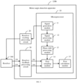
- an electric vehicle 1000 specifically includes a motor drive system 100 configured to drive the vehicle to travel, an in-vehicle energy system 200 configured to provide energy, and an auxiliary system 300.
- the motor drive system 100 includes a vehicle control unit 110, a motor controller 120, a drive motor 130, a transmission apparatus 140, and a wheel 150.
- the in-vehicle energy system 200 includes a power battery 210, a battery management system 220, and a charger 230.
- the vehicle control unit (VCU) 110 is also referred to as a power assembly controller, is a core control component of the entire vehicle, and is equivalent to a brain of the vehicle. After collecting an accelerator pedal signal, a brake pedal signal, and other component signals and making corresponding determining, the vehicle control unit 110 controls actions of lower-layer component controllers, to drive the vehicle to normally travel.
- main functions of the vehicle control unit include drive torque control, brake energy optimization control, vehicle energy management, CAN (Controller Area Network, controller area network) maintenance and management, fault diagnosis and processing, vehicle status monitoring, and the like.
- the vehicle control unit controls operation of the vehicle. Therefore, performance of the vehicle control unit directly determines stability and safety of the vehicle.
- the motor controller 120 is an integrated circuit that actively works to control the drive motor 130 to work based on a specified direction, speed, angle, and response time, and is communicatively connected to the vehicle control unit 110.
- the motor controller 120 is configured to convert, based on an instruction of a gear, a throttle, a brake, or the like, electric energy stored in the power battery 210 into electric energy needed for the drive motor 130, to control a traveling state such as startup and operation, a forward/backward speed, or a climbing force of the electric vehicle 1000, or help the electric vehicle 1000 brake and store some brake energy in the power battery 210.
- the drive motor 130 (commonly referred to as a "motor”) is an electromagnetic apparatus that implements electric energy conversion or transmission according to the law of electromagnetic induction, and is electrically connected to the motor controller 120 and mechanically connected to the transmission apparatus 140.
- the drive motor 130 is mainly configured to generate a drive torque as a power source of the wheel 150.
- the drive motor 130 may further convert mechanical energy into electric energy; in other words, may be further used as a generator.
- the drive motor 130 may be a permanent-magnet synchronous motor (PMSM, Permanent-Magnet Synchronous Motor)-type motor.
- the drive motor 130 may include a stator and a rotor.
- the stator includes a stator winding.
- the rotor may rotate about a central axis relative to the stator.
- the drive motor 130 may be controlled by enabling a common sine current to flow through the stator winding. An amplitude and a frequency of the current can be changed to control torque and a rotation speed of the rotor.
- the stator current generates an electromagnetic field, and the electromagnetic field interacts with a permanent magnet used as a component of the rotor. The electromagnetic field enables the rotor to rotate.
- the drive motor 130 may be a three-phase motor. That is, the stator winding may include three separate phase windings.
- a three-phase voltage wave or a three-phase current wave is applied to the phase windings.
- the three-phase wave enables signals of all phases to be separated from each other based on a phase difference of 120 degrees.
- the transmission apparatus 140 is further mechanically connected to the wheel 150, and is configured to transmit the power source generated by the drive motor 130 to the wheel 150, to drive the electric vehicle 1000 to travel.
- the transmission apparatus 140 may include a drive shaft (not shown) connected between two wheels 150 and a differential (not shown) disposed on the drive shaft.
- the power battery 210 is electrically connected to the motor controller 120, and is configured to store and provide electric energy.
- the power battery 210 includes but is not limited to a lead-acid battery, a lithium iron phosphate battery, a nickel-hydrogen battery, a nickel-cadmium battery, and the like. In some embodiments, the power battery 210 may alternatively include a supercapacitor.
- the battery management system 220 is electrically connected to the power battery 210, and is communicatively connected to the vehicle control unit 110.
- the battery management system 220 is configured to monitor and estimate states of the power battery 210 in different working conditions, to improve utilization of the power battery 210, and prevent the power battery 210 from being overcharged or over-discharged, thereby prolonging a service life of the power battery 210.
- main functions of the battery management system 220 may include real-time battery physical parameter monitoring, battery status estimation, online diagnosis and warning, charging, discharging, and pre-charging control, balancing management and heat management, and the like.
- the charger 230 is electrically connected to the power battery 210, and is configured to be connected to an external power supply to charge the power battery 210. Specifically, when the electric vehicle 1000 is connected to an external power supply (such as a charging pile), the charger 230 converts an alternating current provided by the external power supply into a direct current, to charge the power battery 210.
- the battery management system 220 is further connected to the charger 230 to monitor a charging process of the power battery 210.
- the auxiliary system 300 includes a DC/DC converter 310, an auxiliary battery 320, a low-voltage load 330, and a high-voltage load 340.
- One end of the DC/DC converter 310 is connected to the power battery 210, and the other end of the DC/DC converter 310 is connected to both the auxiliary battery 320 and the low-voltage load 330.
- the DC/DC converter 310 is configured to: after converting a high voltage (such as 380 V) output by the power battery 210 into a low voltage (such as 12 V), charge the auxiliary battery 320 and supply power to the low-voltage load 330.
- the low-voltage load 330 includes low-voltage vehicle accessories such as a cooling pump, a fan, a heater, a power steering apparatus, and a brake.
- the auxiliary battery 320 may also supply power to the low-voltage load 330.
- the power battery 210 is further connected to the high-voltage load 340 to supply power to the high-voltage load 340.
- the high-voltage load 340 includes a PTC heater, an air conditioning unit, and the like.
- the vehicle network may include a plurality of channels for communication.
- a channel of the vehicle network may be, for example, a serial bus of a controller area network (Controller Area Network, CAN).
- One of the channels of the vehicle network may include Ethernet defined by the Institute of Electrical and Electronics Engineers (IEEE) 802 standard family.
- Other channels of the vehicle network may include a discrete connection between modules and may include a power signal from the auxiliary battery 320.
- Different signals may be transmitted by using different channels of the vehicle network. For example, a video signal may be transmitted by using a high-speed channel (such as Ethernet), and a control signal may be transmitted by using a CAN or a discrete signal.
- the vehicle network may include any hardware component and software component assisting in signal and data transmission between modules.
- the vehicle network is not shown in FIG. 1 , but it may be implied that the vehicle network may be connected to any electronic module in the electric vehicle 1000.
- the vehicle network may be connected to the vehicle control unit 110 to coordinate operations of the components.
- the schematic structure in this embodiment of this application constitutes no specific limitation on the electric vehicle 1000.
- the electric vehicle 1000 may include more or fewer components than those shown in the figure, combine some components, split some components, or have different component arrangements.
- the component shown in the figure may be implemented by using hardware, software, or a combination of software and hardware.
- the motor controller 120 includes an inverter circuit 120a and a motor angle detection apparatus 120b.
- An input end of the inverter circuit 120a is connected to the power battery 210, and an output end of the inverter circuit 120a is connected to the drive motor 130.
- the inverter circuit 120a is configured to convert a high-voltage direct current output by the power battery 210 into an alternating current (such as a three-phase alternating current), to enable the drive motor 130 to work.
- the motor angle detection apparatus 120b is connected to the drive motor 130 by using a resolver (resolver/transformer) 160, to detect an electrical angle of the drive motor 130.
- the resolver 160 is a sensor that accurately measures an angular position and speed of a rotation component such as a motor through a magnetic coupling effect between a primary winding and two secondary windings.
- the primary winding and the two orthogonal secondary windings are respectively mounted on a rotor and a stator of the motor, and a sine feedback signal and a cosine feedback signal are respectively obtained from the two secondary windings through coupling based on an exciting signal applied to the primary winding.
- the sine feedback signal and the cosine feedback signal may be collectively referred to as a resolver feedback signal.
- Angular position and rotation speed information of the rotor of the motor may be obtained after the sine feedback signal and the cosine feedback signal are demodulated and converted.
- a magnetoresistive resolver is usually used in the drive motor 130 of the electric vehicle 1000.
- the magnetoresistive resolver is a special form of the resolver 160, and implements conversion between electrical signals by using a magnetoresistive principle.
- a feature of the magnetoresistive resolver is that a primary-side winding and a secondary-side winding are both placed in different slots of the stator of the motor and are both fixed and not rotated.
- the primary-side winding means that a sinusoidal exciting current flows into an exciting winding
- the secondary-side winding means that an output signal is generated by using a two-phase coil.
- the schematic structure in this embodiment of this application constitutes no specific limitation on the motor controller 120.
- the motor controller 120 may include more components than those shown in the figure, such as an auxiliary power supply circuit, a charging circuit, and a voltage/current detection circuit.
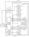
- FIG. 3 is a schematic structural diagram of a motor angle detection apparatus in an embodiment of this application.
- a motor angle detection apparatus 120b includes a microprocessor 10, a resolver exciting processing circuit 20, and a resolver feedback processing circuit 30.
- the resolver exciting processing circuit 20 is electrically connected between the microprocessor 10 and an input end of a resolver 160, and is configured to obtain an exciting signal after filtering and amplifying an exciting modulation signal generated by the microprocessor 10, to drive the resolver 160 to work to output a resolver feedback signal of an electrical angle of a drive motor 130.
- the resolver feedback processing circuit 30 is electrically connected between an output end of the resolver 160 and the microprocessor 10, and is configured to: adjust the resolver feedback signal, and send an adjusted resolver feedback signal to the microprocessor 10.
- the microprocessor 10 includes a signal generation module 11, a signal processing module 12, a phase shift processing module 13, a first sampling module 14, and a first calculation module 15.
- the signal generation module 11 is configured to generate the exciting modulation signal.
- the signal generation module 11 is configured to: generate an exciting fundamental wave signal (a) and a carrier signal (b), and generate the exciting modulation signal after comparing the exciting fundamental wave signal (a) with the carrier signal (b).
- the exciting fundamental wave signal (a) is a sine wave signal, and may be obtained through table lookup.
- the carrier signal (b) is a symmetrical triangular wave signal, and may be implemented by using a counter. Therefore, the exciting modulation signal in this embodiment of this application is a high-frequency PWM (Pulse width modulation, Pulse width modulation) signal that includes an exciting fundamental wave component.
- the signal processing module 12 is configured to determine an exciting symbol (c) based on the exciting fundamental wave signal (a).
- the exciting symbol (c) includes alternate high-level signals and low-level signals.
- the high-level signal corresponds to a part that is of the exciting fundamental wave signal (a) and whose voltage is greater than a reference threshold voltage x
- the low-level signal corresponds to a part that is of the exciting fundamental wave signal (a) and whose voltage is less than the reference threshold voltage x
- a rising edge or a falling edge of the exciting symbol (c) corresponds to a part that is of the exciting fundamental wave signal (a) and whose voltage is equal to the reference threshold voltage x.
- the reference threshold voltage x is a direct current component between 0 V and 5 V, is not specifically limited, and may be determined based on a specific use case. For example, the reference threshold voltage x may be set to 3 V. In this way, a correspondence between the rising edge or the falling edge of the exciting symbol (c) and a zero crossing point of the exciting fundamental wave signal (a) can be established.
- the signal processing module 12 is further configured to determine a zero crossing point signal (d) of the exciting fundamental wave signal (a) based on the exciting symbol (c). In this embodiment of this application, the signal processing module 12 determines the zero crossing point signal of the exciting fundamental wave signal (a) based on the rising edge of the exciting symbol (c).
- the phase shift processing module 13 is configured to perform phase shift processing on the zero crossing point signal (d) to obtain a sampling trigger signal (e), to trigger the first sampling module 14 to sample the resolver feedback signal.
- the microprocessor 10 in this embodiment of this application may determine the exciting symbol (c) based on the exciting fundamental wave signal (a) generated by the signal generation module 11, then determine the zero crossing point signal (d) of the exciting fundamental wave signal based on the exciting symbol (c), and finally perform phase shift processing on the zero crossing point signal (d) to obtain the sampling trigger signal (e), to trigger the first sampling module 14 to sample the resolver feedback signal, without using an external shaping circuit, thereby saving an area of a printed circuit board and improving an integration degree.
- the phase shift processing module 13 performs phase shift processing on the zero crossing point signal (d), so that the zero crossing point of the exciting fundamental wave signal (a) can be dodged, thereby avoiding abnormal sampling of the resolver feedback signal and improving sampling accuracy.
- the first calculation module 15 is configured to calculate an electrical angle of the drive motor 103 based on data collected by the first sampling module 15, to decode the resolver feedback signal after the sampling.
- the first sampling module 14 is a successive approximation register analog to digital converter (Successive Approximation Register ADC, SAR-ADC) with relatively high sampling accuracy.
- SAR-ADC Successessive Approximation Register ADC
- the SAR-ADC further has features such as ease of use and low power consumption, which can reduce system power consumption while facilitating integration.
- a basic converter architecture of the SAR-ADC samples an input signal once on each conversion starting edge, performs bit comparison on each clock edge, and adjusts output of the digital to analog converter by using control logic until the output very closely matches analog input. Therefore, the basic converter architecture needs N clock cycles from an independent external clock to iteratively implement single N-bit conversion.
- a phase shift of the sampling trigger signal (e) relative to the zero crossing point signal (d) is greater than a 90° phase shift of the exciting fundamental wave signal (a) from the zero crossing point to a peak point, and the phase shift can be set.
- the zero crossing point of the exciting fundamental wave signal (a) can be dodged, thereby avoiding a relatively large calculation error generated because a divisor is close to 0.
- the phase shift can be adjusted based on a specific use case, for ease of use by a user.
- an absolute value of a difference between phase shift processing time of the zero crossing point signal (d) and primary reference time is less than a preset threshold.
- the primary reference time is time of phase shift of the exciting fundamental wave signal (a) from the zero crossing point to a peak point and delay time of passing through a resolver sampling feedback loop by the exciting fundamental wave signal (a).
- the delay time of the resolver sampling feedback loop is delay time needed by the exciting fundamental wave signal (a) to pass through the resolver exciting processing circuit 20, the resolver 160, and the resolver feedback processing circuit 30.
- the zero crossing point of the exciting fundamental wave signal (a) can be dodged, to ensure, as far as possible, that sampling is performed near the peak point of the exciting fundamental wave signal (a), thereby avoiding a relatively large calculation error generated because a divisor is close to 0, and improving sampling accuracy.
- the phase shift processing module 13 performs phase shift processing on the zero crossing point signal (d) to obtain a sampling trigger signal corresponding to a peak of a signal obtained after the exciting signal passes through a resolver sampling feedback loop.
- the signal obtained after the exciting signal passes through the resolver sampling feedback loop is shown as (f) in FIG. 4 . In this way, it can be ensured that sampling is performed near a peak point of the exciting fundamental wave signal, thereby avoiding a relatively large calculation error generated because a divisor is close to 0, and improving sampling accuracy.
- the signal processing module 12 determines the zero crossing point signal of the exciting fundamental wave signal (a) based on the rising edge and the falling edge of the exciting symbol (c). That is, two times of sampling may be performed near two points of the exciting fundamental wave signal (a): a peak and a valley, so that two times of sampling trigger may be implemented in one exciting period.
- Torque safety is a most important function safety target of the motor controller 120, and is generally defined as no unexpected torque acceleration or deceleration, or unexpected startup.
- a torque function safety target ASIL Automotive Safety Integrity Level, automotive safety integrity level
- a higher ASIL indicates higher diagnosis coverage of a circuit related to function safety and a lower corresponding hardware random failure probability metric.
- description is provided by using an example that the torque function safety ASIL of the motor controller 120 is the level C.
- FIG. 6 is a schematic structural diagram of a motor angle detection apparatus 120b in another embodiment of this application.
- the motor angle detection apparatus 120b further includes a diagnosis signal sampling circuit 40.
- the diagnosis signal sampling circuit 40 is electrically connected to both the resolver exciting processing circuit 20 and the resolver feedback processing circuit 30, and is configured to: collect the exciting signal and the resolver feedback signal obtained after the processing by the resolver feedback processing circuit 30, and generate a corresponding loopback detection signal.
- the microprocessor 10 further includes a first diagnosis module 18.
- the first diagnosis module 18 is configured to diagnose, based on the loopback detection signal, whether the exciting processing circuit 20 and the feedback processing circuit 30 are faulty.
- the microprocessor 10 further includes a second sampling module 16, a second calculation module 17, and a second diagnosis module 19.
- the second sampling module 16 is configured to sample the resolver feedback signal.
- the second calculation module 17 is configured to calculate an electrical angle of the drive motor 130 based on data collected by the second sampling module 16. One electrical angle is used for torque control and the other electrical angle is used for torque monitoring.
- a system of the microprocessor 10 usually uses an EGAS three-layer architecture.
- a main design concept of an EGAS architecture of the motor controller is hierarchically designing a control system; in other words, dividing the control system into a function layer (Level 1), a function monitoring layer (Level 2), and a processor monitoring layer (Level 3).
- the function layer (Level 1) mainly implements a basic function of the control system, that is, outputs torque for the motor controller 120.
- the function monitoring layer (Level 2) mainly monitors the level 1, and includes a component monitoring function, an input/output variable diagnosis function, and a function of performing a system fault response after detecting a fault, for example, monitors an actual output value for torque calculation to determine whether level 1 software is correct. Once a fault is diagnosed, a system fault response is triggered and executed by the level 2.
- the processor monitoring layer (Level 3) mainly monitors, through question and answer, whether a processor of the level 2 is faulty, and needs to be implemented by an independent application-specific integrated circuit ASIC or microprocessor. After a fault occurs, a system fault response is triggered and executed independently of the level 1.
- the second sampling module 16 may be an SAR-ADC or a ⁇ analog to digital converter SD-ADC with higher sampling accuracy. Therefore, the two analog to digital converters of the level 1/level 2 may be an SD-ADC/SD-ADC, an SAR-ADC/SAR-ADC, or an SD-ADC/SAR-ADC.
- This embodiment of this application uses SD-ADC/SAR-ADC heterogeneous redundancy as an example for description. It should be noted that the SD-ADC includes a clock, and therefore does not need to be triggered by an external clock signal.
- the first sampling module 14 is an SAR-ADC and is located at the level 2 layer.
- the second sampling module 16 is located at the level 1 layer, and includes an SD-ADC 16a and a demodulation module 16b.
- the signal generation module 11, the signal processing module 12, the phase shift processing module 13, and the second calculation module 17 are all located at the level 1 layer.
- the first calculation module 15, the first diagnosing module 18, and the second diagnosing module 19 are all located at the level 2 layer.
- the SD-ADC 16a is configured to sample the resolver feedback signal to obtain a sampled signal
- the demodulation module 16b is configured to demodulate the sampled signal to separate the exciting fundamental wave signal from the sampled signal.
- the resolver feedback signal includes a sine feedback signal and a cosine feedback signal.
- the resolver feedback processing circuit 30 is configured to convert the sine resolver feedback signal into a sine single-ended signal and then output the sine single-ended signal to a sine sampling channel x1 of the SAR-ADC.
- the feedback processing circuit 30 is further configured to convert the cosine resolver feedback signal into a cosine single-ended signal and output the cosine single-ended signal to a cosine sampling channel y1 of the SAR-ADC.
- the resolver feedback processing circuit 30 is further configured to convert the sine feedback signal into a sine differential signal that matches a level of an SD-ADC port, and then output the sine differential signal to a sine sampling channel x2 of the SD-ADC.
- the resolver feedback processing circuit 30 is further configured to convert the cosine resolver feedback signal into a cosine differential signal that matches the level of the SD-ADC port, and then output the cosine differential signal to a cosine sampling channel y2 of the SD-ADC.
- FIG. 8 is a flowchart of a sampling trigger method in an embodiment of this application.
- the sampling trigger method is applied to the microprocessor 10 shown in FIG. 3 , FIG. 6 , or FIG. 7 .
- the sampling trigger method includes the following step: Step S 11: Generate an exciting fundamental wave signal to drive a resolver to work.
- the generating an exciting fundamental wave signal to drive the resolver to work includes: further generating a carrier signal while generating the exciting fundamental wave signal, and comparing the exciting fundamental wave signal with the carrier signal to generate an exciting modulation signal, where an exciting signal is obtained after the exciting modulation signal is filtered and amplified, to drive the resolver to work.
- Step S12 Determine an exciting symbol based on the exciting fundamental wave signal, where the exciting symbol includes alternate high-level signals and low-level signals.
- the high-level signal corresponds to a part that is of the exciting fundamental wave signal and whose voltage is greater than a reference threshold voltage
- the low-level signal corresponds to a part that is of the exciting fundamental wave signal and whose voltage is less than the reference threshold voltage
- a rising edge or a falling edge of the exciting symbol corresponds to a part that is of the exciting fundamental wave signal and whose voltage is equal to the reference threshold voltage.
- the reference threshold voltage is a direct current component between 0 V and 5 V.
- Step S 13 Determine a zero crossing point signal of the exciting fundamental wave signal based on the exciting symbol.
- the determining a zero crossing point signal of the exciting fundamental wave signal based on the exciting symbol includes: determining the zero crossing point signal of the exciting fundamental wave signal based on the rising edge and/or the falling edge of the exciting symbol.
- Step S14 Perform phase shift processing on the zero crossing point signal to obtain a sampling trigger signal, to trigger a first analog to digital conversion module to sample a resolver feedback signal.
- a phase shift of the sampling trigger signal relative to the zero crossing point signal is greater than a 90° phase shift of the exciting fundamental wave signal from a zero crossing point to a peak point, and the phase shift can be set.
- an absolute value of a difference between phase shift processing time of the zero crossing point signal and primary reference time is less than a preset threshold, and the primary reference time is time of phase shift of the exciting fundamental wave signal from a zero crossing point to a peak point and delay time of passing through a resolver sampling feedback loop by the exciting fundamental wave signal.
- the performing phase shift processing on the zero crossing point signal to obtain a sampling trigger signal includes: performing phase shift processing on the zero crossing point signal to obtain a sampling trigger signal corresponding to a peak and/or a valley of a signal obtained after the exciting signal passes through a resolver sampling feedback loop.
- FIG. 9 is a flowchart of a sampling trigger method in another embodiment of this application. Different from that in FIG. 8 , after the sampling, the sampling trigger method further includes the following step:
- Step S 15 Calculate an electrical angle of a drive motor based on collected data.
- a sequence of the steps of the method in the embodiments of this application may be adjusted, combined, or removed based on an actual requirement.
- All or some of the foregoing embodiments may be implemented by using software, hardware, firmware, or any combination thereof.
- the embodiments may be implemented completely or partially in a form of a computer program product.
- the computer program product includes one or more computer instructions.
- the computer may be a general-purpose computer, a dedicated computer, a computer network, or other programmable apparatuses.
- the computer instructions may be stored in a computer-readable storage medium or may be transmitted from a computer-readable storage medium to another computer-readable storage medium.
- the computer instructions may be transmitted from a website, computer, server, or data center to another website, computer, server, or data center in a wired (for example, a coaxial cable, an optical fiber, or a digital subscriber line) or wireless (for example, infrared, radio, or microwave) manner.
- the computer-readable storage medium may be any usable medium accessible by a computer, or a data storage device, such as a server or a data center, integrating one or more usable media.
- the usable medium may be a magnetic medium (for example, a floppy disk, a hard disk, or a magnetic tape), an optical medium (for example, a DVD), a semiconductor medium (for example, a Solid State Disk), or the like.
Landscapes
- Engineering & Computer Science (AREA)
- Physics & Mathematics (AREA)
- General Physics & Mathematics (AREA)
- Power Engineering (AREA)
- Theoretical Computer Science (AREA)
- Transmission And Conversion Of Sensor Element Output (AREA)
Claims (20)
- Abtastauslöserverfahren, das auf einen Mikroprozessor (10) angewendet wird, wobei der Mikroprozessor (10) durch Verwenden eines Resolvers (160) mit einem Antriebsmotor (130) verbunden ist und konfiguriert ist, um ein Resolverrückkopplungssignal abzutasten, das von einem elektrischen Winkel des Antriebsmotors (130) stammt und das durch den Resolver (160) ausgegeben wird, und das Abtastauslöserverfahren umfasst:Erzeugen (S11) eines Erregergrundwellensignals (a), um den Resolver (160) zum Arbeiten anzutreiben;Bestimmen (S12) eines Erregersymbols (c) basierend auf dem Erregergrundwellensignal (a), wobei das Erregersymbol (c) aus abwechselnden starken Signalen und schwachen Signalen besteht;Bestimmen (S13) eines Nulldurchgangspunktsignals (d) des Erregergrundwellensignals (a) basierend auf dem Erregersymbol (c); undDurchführen (S14) einer Phasenverschiebungsverarbeitung an dem Nulldurchgangspunktsignal (d), um ein Abtastauslösersignal (e) zu erhalten, um den Mikroprozessor (10) auszulösen, um das Resolverrückkopplungssignal abzutasten.
- Abtastauslöserverfahren nach Anspruch 1, wobei der Mikroprozessor (10) ein erstes Abtastmodul (14) umfasst und das erste Abtastmodul (14) ein Analog-Digital-Wandler mit sukzessivem Approximationsregister (SAR-ADC) ist; und das Auslösen des Mikroprozessors (10), um das Resolverrückkopplungssignal abzutasten, umfasst: Auslösen des SAR-ADC, um das Resolverrückkopplungssignal abzutasten.
- Abtastauslöserverfahren nach Anspruch 1 oder 2, wobei das starke Signal einem Teil entspricht, der von dem Erregergrundwellensignal (a) stammt und dessen Spannung über einer Referenzschwellenspannung (x) liegt, das schwache Signal einem Teil entspricht, der von dem Erregergrundwellensignal (a) stammt und dessen Spannung kleiner als die Referenzschwellenspannung (x) ist, und eine steigende Flanke oder eine fallende Flanke des Erregersymbols (c) einem Teil entspricht, der aus dem Erregergrundwellensignal (a) stammt und dessen Spannung gleich der Referenzschwellenspannung (x) ist.
- Abtastauslöserverfahren nach Anspruch 3, wobei das Bestimmen (S12) eines Nulldurchgangspunktsignals (d) des Erregergrundwellensignals (a) basierend auf dem Erregersymbol (c) umfasst: Bestimmen des Nulldurchgangspunktsignals (d) des Erregergrundwellensignals (a) basierend auf der steigenden Flanke und/oder der fallenden Flanke des Erregersymbols (c).
- Abtastauslöserverfahren nach einem der Ansprüche 1 bis 4, wobei eine Phasenverschiebung des Abtastauslösersignals (e) relativ zu dem Nulldurchgangspunktsignal (d) über einer 90°-Phasenverschiebung des Erregergrundgellensignals (a) von einem Nulldurchgangspunkt zu einem Spitzenpunkt liegt, und die Phasenverschiebung eingestellt werden kann.
- Abtastauslöserverfahren nach einem der Ansprüche 1 bis 4, wobei ein Absolutwert einer Differenz zwischen der Phasenverschiebungsverarbeitungszeit des Nulldurchgangspunktsignals (d) und der primären Referenzzeit kleiner als ein voreingestellter Schwellenwert ist und die primäre Referenzzeit eine Zeit der Phasenverschiebung des Erregergrundwellensignals (a) von einem Nulldurchgangspunkt zu einem Spitzenpunkt und eine Verzögerungszeit eines Hindurchverlaufens einer Resolverabtastrückkopplungsschleife durch das Erregergrundwellensignal (a) ist.
- Abtastauslöserverfahren nach einem der Ansprüche 1 bis 4, wobei das Erzeugen (S11) eines Erregergrundwellensignals (a), um den Resolver (160) anzutreiben, um zu arbeiten umfasst: ferner Erzeugen eines Trägersignals (b) während des Erzeugens des Erregergrundwellensignals (a) und Vergleichen des Erregergrundwellensignals (a) mit dem Trägersignal (b), um ein Erregermodulationssignal zu erzeugen, wobei ein Erregersignal erhalten wird, nachdem das Erregermodulationssignal gefiltert und verstärkt wird, um den Resolver (160) anzutreiben, zu arbeiten; und
das Durchführen (S14) der Phasenverschiebungsverarbeitung an dem Nulldurchgangspunktsignal (d), um ein Abtastauslösersignal (e) zu erhalten, umfasst: Durchführen einer Phasenverschiebungsverarbeitung an dem Nulldurchgangspunktsignal (d), um ein Abtastauslösersignal (e) zu erhalten, das einer Spitze und/oder einem Tal eines Signals entspricht, das erhalten wird, nachdem das Erregersignal (a) durch eine Resolverabtastrückkopplungsschleife hindurchverläuft. - Abtastauslöserverfahren nach einem der Ansprüche 1 bis 7, wobei nach dem Auslösen des Mikroprozessors (10), um das Resolverrückkopplungssignal abzutasten, das Abtastauslöserverfahren ferner umfasst:
Berechnen (S15) des elektrischen Winkels des Antriebsmotors (130) basierend auf gesammelten Daten. - Mikroprozessor (10), der durch Verwenden eines Resolvers (160) mit einem Antriebsmotor (130) verbunden ist und konfiguriert ist, um ein Resolverrückkopplungssignal abzutasten, das von einem elektrischen Winkel des Antriebsmotors (130) stammt und das von dem Resolver (160) ausgegeben wird, wobei der Mikroprozessor (10) umfasst:ein Signalerzeugungsmodul (11), das konfiguriert ist, um ein Erregergrundwellensignal (a) zu erzeugen, um den Resolver (160) anzutreiben, um zu arbeiten;ein Signalverarbeitungsmodul (12), das konfiguriert ist, um ein Erregersymbol (c) basierend auf dem Erregergrundwellensignal (a) zu bestimmen, wobei das Erregersymbol (c) aus abwechselnden starken Signalen und schwachen Signalen besteht, und das Signalverarbeitungsmodul (12) ferner konfiguriert ist, um ein Nulldurchgangspunktsignal (d) des Erregergrundwellensignals (a) basierend auf dem Erregersymbol (c) zu bestimmen; undein Phasenverschiebungsverarbeitungsmodul (13), das konfiguriert ist, um eine Phasenverschiebungsverarbeitung an dem Nulldurchgangspunktsignal durchzuführen, um ein Abtastauslösersignal (e) zu erhalten, um den Mikroprozessor (10) auszulösen, um das Resolverrückkopplungssignal abzutasten.
- Mikroprozessor (10) nach Anspruch 9, wobei der Mikroprozessor (10) ein Analog-Digital-Wandler mit sukzessivem Approximationsregister (SAR-ADC) umfasst; und das Phasenverschiebungsverarbeitungsmodul (13) konfiguriert ist, um eine Phasenverschiebungsverarbeitung auf dem Nulldurchgangspunktsignal (d) durchzuführen, um das Abtastauslösersignal (e) zu erhalten, um den SAR-ADC auszulösen, um das Resolverrückkopplungssignal abzutasten.
- Mikroprozessor (10) nach Anspruch 9 oder 10, wobei das starke Signal einem Teil entspricht, der von dem Erregergwellensignal (a) stammt und dessen Spannung über einer Referenzschwellenspannung (x) liegt, wobei das schwache Signal einem Teil entspricht, der von dem Erregergrundwellensignal (a) stammt und dessen Spannung kleiner als die Referenzschwellenspannung (x) ist, und eine steigende Flanke oder eine fallende Flanke des Erregersymbols (c) einem Teil entspricht, der von dem Erregergrundwellensignal (a) stammt und dessen Spannung gleich der Referenzschwellenspannung (x) ist.
- Mikroprozessor (10) nach Anspruch 11, wobei das Signalverarbeitungsmodul (12) konfiguriert ist, um das Nulldurchgangspunktsignal (d) des Erregergrundwellensignals (a) basierend auf der steigenden Flanke und/oder der fallenden Flanke des Erregersymbols (c) zu bestimmen.
- Mikroprozessor (10) nach einem der Ansprüche 9 bis 12, wobei eine Phasenverschiebung des Abtastauslösersignals (e) relativ zu dem Nulldurchgangspunktsignal (d) über einer 90°-Phasenverschiebung des Erregergrundwellensignals (a) von einem Nulldurchgangspunkt zu einem Spitzenpunkt liegt, und die Phasenverschiebung eingestellt werden kann.
- Mikroprozessor (10) nach einem der Ansprüche 9 bis 12, wobei ein Absolutwert einer Differenz zwischen der Phasenverschiebungsverarbeitungszeit des Nulldurchgangspunktsignals und der primären Referenzzeit kleiner als ein voreingestellter Schwellenwert ist und die primäre Referenzzeit eine Zeit der Phasenverschiebung des Erregergrundwellensignals (a) von einem Nulldurchgangspunkt zu einem Spitzenpunkt und eine Verzögerungszeit des Hindurchverlaufens einer Resolverabtastrückkopplungsschleife durch das Erregergrundwellensignal (a) ist.
- Mikroprozessor (10) nach einem der Ansprüche 9 bis 12, wobei das Signalerzeugungsmodul (11) ferner konfiguriert ist zum: Erzeugen eines Trägersignals (b) und Vergleichen des Erregergrundwellensignals (a) mit dem Trägersignal (b), um ein Erregermodulationssignal zu erzeugen, wobei ein Erregersignal erhalten wird, nachdem das Erregermodulationssignal gefiltert und verstärkt wird, um den Resolver (160) anzutreiben, um zu arbeiten; und das Phasenverschiebungsverarbeitungsmodul (13) konfiguriert ist, um eine Phasenverschiebungsverarbeitung auf dem Nulldurchgangspunktsignal (d) durchzuführen, um ein Abtastauslösersignal (e) zu erhalten, das einer Spitze und/oder einem Tal eines Signals entspricht, das erhalten wird, nachdem das Erregersignal eine Resolverabtastrückkopplungsschleife hindurchverläuft.
- Mikroprozessor (10) nach einem der Ansprüche 9 bis 15, wobei der Mikroprozessor (10) ferner ein erstes Berechnungsmodul (15) umfasst und das erste Berechnungsmodul (15) konfiguriert ist, um einen elektrischen Winkel des Antriebsmotors (130) basierend auf gesammelten Daten zu berechnen.
- Motorsteuervorrichtung (120), umfassend eine Wechselrichterschaltung (120a), wobei ein Eingangsende der Wechselrichterschaltung mit einer Leistungsbatterie (210) verbunden ist und ein Ausgangsende der Wechselrichterschaltung (120a) mit einem Antriebsmotor (130) verbunden ist; die Wechselrichterschaltung (120a) konfiguriert ist, um einen Hochspannungsgleichstrom, der durch die Leistungsbatterie (210) ausgegeben wird, in einen Wechselstrom umzuwandeln, um den Antriebsmotor (130) zu aktivieren, um zu arbeiten; und die Motorsteuervorrichtung (120) ferner den Mikroprozessor (10) nach einem der Ansprüche 9 bis 16 umfasst, wobei der Mikroprozessor (10) unter Verwendung eines Resolvers (160) mit dem Antriebsmotor (130) verbunden ist.
- Motorsteuervorrichtung (120) nach Anspruch 17, wobei die Motorsteuervorrichtung (120) ferner eine Resolvererregerverarbeitungsschaltung (20) und eine Resolverrückkopplungsverarbeitungsschaltung (30) umfasst; die Resolvererregerverarbeitungsschaltung (20) zwischen dem Mikroprozessor (10) und dem Resolver elektrisch verbunden ist und konfiguriert ist, um ein Erregermodulationssignal zu filtern und zu verstärken; und die Resolverrückkopplungsverarbeitungsschaltung (30) zwischen dem Resolver (160) und dem Mikroprozessor (10) verbunden ist und konfiguriert ist, um ein Resolverrückkopplungssignal in ein unsymmetrisches Signal umzuwandeln.
- Motorsteuervorrichtung (120) nach Anspruch 18, wobei die Motorsteuervorrichtung (120) ferner eine Diagnosesignalabtastschaltung (40) umfasst; und die Diagnosesignalabtastschaltung (40) sowohl mit der Resolvererregerverarbeitungsschaltung (20) als auch mit der Resolverrückkopplungsverarbeitungsschaltung (30) elektrisch verbunden ist und konfiguriert ist zum: Sammeln eines Erregersignals und eines Resolverrückkopplungssignals, das nach dem Verarbeiten durch die Resolverrückkopplungsverarbeitungsschaltung (30) erhalten wird, und Erzeugen eines entsprechenden Rückschleifenerfassungssignals;der Mikroprozessor (10) ferner ein erstes Diagnosemodul (18) umfasst; und das erste Diagnosemodul (18) konfiguriert ist, um, basierend auf dem Rückschleifenerfassungssignal, zu diagnostizieren, ob die Resolvererregerverarbeitungsschaltung (20) und die Resolverrückkopplungsverarbeitungsschaltung (30) fehlerhaft sind;der Mikroprozessor (10) ferner ein zweites Abtastmodul (16), ein zweites Berechnungsmodul (17) und ein zweites Diagnosemodul (19) umfasst; das zweite Abtastmodul (16) konfiguriert ist, um das Resolverrückkopplungssignal abzutasten; und das zweite Berechnungsmodul (17) konfiguriert ist, um einen elektrischen Winkel des Antriebsmotors (130) basierend auf Daten zu berechnen, die durch das zweite Abtastmodul (16) gesammelt werden, wobei ein elektrischer Winkel für eine Drehmomentsteuerung verwendet wird und der andere elektrische Winkel für eine Drehmomentüberwachung verwendet werden; unddas zweite Diagnosemodul (19) konfiguriert ist, um in Echtzeit Daten zu diagnostizieren, die durch ein erstes Abtastmodul (14) und das zweite Abtastmodul (16) gesammelt werden, und ferner konfiguriert ist, um die zwei elektrischen Winkel in Echtzeit zu diagnostizieren, so dass die elektrischen Winkel eine Eingangsgrößenanforderung eines Drehmomentfunktionssicherheitsentwurfs erfüllen.
- Elektrofahrzeug (1000), umfassend die Motorsteuervorrichtung (120) nach einem der Ansprüche 17 bis 19.
Applications Claiming Priority (1)
| Application Number | Priority Date | Filing Date | Title |
|---|---|---|---|
| PCT/CN2020/093008 WO2021237603A1 (zh) | 2020-05-28 | 2020-05-28 | 采样触发方法、微处理器、电机控制器及电动汽车 |
Publications (3)
| Publication Number | Publication Date |
|---|---|
| EP3937366A1 EP3937366A1 (de) | 2022-01-12 |
| EP3937366A4 EP3937366A4 (de) | 2022-06-15 |
| EP3937366B1 true EP3937366B1 (de) | 2023-02-22 |
Family
ID=75413938
Family Applications (1)
| Application Number | Title | Priority Date | Filing Date |
|---|---|---|---|
| EP20922463.3A Active EP3937366B1 (de) | 2020-05-28 | 2020-05-28 | Abtastauslöseverfahren, mikroprozessor, motorregler und elektrisches fahrzeug |
Country Status (4)
| Country | Link |
|---|---|
| US (1) | US11804795B2 (de) |
| EP (1) | EP3937366B1 (de) |
| CN (1) | CN112672911B (de) |
| WO (1) | WO2021237603A1 (de) |
Families Citing this family (4)
| Publication number | Priority date | Publication date | Assignee | Title |
|---|---|---|---|---|
| EP3927938A4 (de) * | 2019-02-19 | 2023-02-22 | Probe Technology Services, Inc. | Neuer kernpositionssensor |
| CN114079415A (zh) * | 2021-10-09 | 2022-02-22 | 华为数字能源技术有限公司 | 一种电机角度检测装置、电机控制器以及电动汽车 |
| CN113959465A (zh) * | 2021-10-18 | 2022-01-21 | 深圳英恒电子有限公司 | 一种旋转变压器的信号补偿方法和装置 |
| CN117270487B (zh) * | 2023-11-17 | 2024-01-23 | 北京芯驰半导体科技有限公司 | 模拟信号的采样控制系统、方法及芯片 |
Family Cites Families (22)
| Publication number | Priority date | Publication date | Assignee | Title |
|---|---|---|---|---|
| US5229697A (en) * | 1992-01-30 | 1993-07-20 | Siemens Industrial Automation, Inc. | Sampling bipolar peak detector for sensing a non-symmetrical decay of an AC voltage signal |
| US5204603A (en) * | 1992-01-30 | 1993-04-20 | Siemens Industrial Automation, Inc. | Open circuit detection for a pulsed resolver position sensing system |
| US5200683A (en) * | 1992-01-30 | 1993-04-06 | Siemens Industrial Automation, Inc. | Method for optimizing sampling rates for position tracking for motion control systems |
| US5323309A (en) * | 1992-01-30 | 1994-06-21 | Siemens Industrial Automation, Inc. | Algorithm for optimizing data sampling in a discrete periodic system with a bounded rate of change for the discrete system periods |
| US5710509A (en) * | 1995-10-30 | 1998-01-20 | Atsutoshi Goto | Phase difference detection device for an inductive position detector |
| EP2128975B1 (de) * | 2006-12-05 | 2014-08-27 | Byd Company Limited | Steuereinrichtung und verfahren zur bestimmung der rotorlage eines motors |
| US8594981B2 (en) * | 2008-06-22 | 2013-11-26 | United Electronic Industries | Dynamically powering a position and angle digital detection and simulation output |
| JP5183666B2 (ja) * | 2010-04-14 | 2013-04-17 | 三菱電機株式会社 | ブラシレスモータの回転位置検出装置 |
| GB201006394D0 (en) * | 2010-04-16 | 2010-06-02 | Dyson Technology Ltd | Controller for a brushless motor |
| JP5865059B2 (ja) * | 2011-12-19 | 2016-02-17 | 横河電機株式会社 | 波形測定器 |
| IN2015KN00376A (de) * | 2012-08-21 | 2015-07-10 | Allison Transm Inc | |
| US10491095B2 (en) * | 2014-10-06 | 2019-11-26 | Ford Global Technologies, Llc | Dynamic IGBT gate drive for vehicle traction inverters |
| CN104527773A (zh) * | 2014-11-24 | 2015-04-22 | 清华大学苏州汽车研究院(相城) | 一种基于旋转变压器软件解码的电动助力转向系统 |
| CN105222814A (zh) * | 2015-11-04 | 2016-01-06 | 上海无线电设备研究所 | 多圈记忆旋转变压器解码电路及其位置解算方法 |
| US9897469B2 (en) * | 2016-01-26 | 2018-02-20 | GM Global Technology Operations LLC | Resolver phase compensation |
| US10267819B2 (en) * | 2016-02-04 | 2019-04-23 | GM Global Technology Operations LLC | Method and apparatus to monitor a resolver |
| CN107547069B (zh) * | 2017-09-18 | 2024-04-09 | 苏州博牛电气有限公司 | 一种旋变激磁信号发生系统及发生方法 |
| CN111130561B (zh) * | 2018-10-31 | 2021-03-23 | 广州汽车集团股份有限公司 | 信号采样方法、装置、计算机设备和存储介质 |
| EP3708965B1 (de) * | 2019-03-12 | 2022-06-01 | Danfoss Editron Oy | Positioniervorrichtung zur erzeugung eines drehpositionssignals und erregungsvorrichtung zur herstellung eines anregungssignals für einen resolver |
| CN110233588A (zh) * | 2019-06-18 | 2019-09-13 | 山东理工大学 | 一种电动汽车驱动用永磁同步电机转子位置检测冗余装置和控制方法 |
| CN110794343B (zh) * | 2019-10-14 | 2021-10-26 | 中车永济电机有限公司 | 一种旋转变压器接线自检测系统 |
| CN110943670B (zh) * | 2019-12-30 | 2021-10-01 | 中国科学院电工研究所 | 一种电机转子位置获取方法及系统 |
-
2020
- 2020-05-28 CN CN202080004988.2A patent/CN112672911B/zh active Active
- 2020-05-28 WO PCT/CN2020/093008 patent/WO2021237603A1/zh unknown
- 2020-05-28 EP EP20922463.3A patent/EP3937366B1/de active Active
-
2021
- 2021-10-06 US US17/495,754 patent/US11804795B2/en active Active
Also Published As
| Publication number | Publication date |
|---|---|
| CN112672911A (zh) | 2021-04-16 |
| EP3937366A1 (de) | 2022-01-12 |
| US20220045640A1 (en) | 2022-02-10 |
| CN112672911B (zh) | 2024-02-09 |
| US11804795B2 (en) | 2023-10-31 |
| WO2021237603A1 (zh) | 2021-12-02 |
| EP3937366A4 (de) | 2022-06-15 |
Similar Documents
| Publication | Publication Date | Title |
|---|---|---|
| EP3944487B1 (de) | Motorwinkeldetektions- und -diagnosevorrichtung, motorsteuergerät, elektrisches fahrzeug und verfahren | |
| EP3937366B1 (de) | Abtastauslöseverfahren, mikroprozessor, motorregler und elektrisches fahrzeug | |
| JP5055246B2 (ja) | 回転電機の制御装置 | |
| JP5626468B2 (ja) | 車両および車両の制御方法 | |
| US8502411B2 (en) | Power limiting apparatus for electric system, power limiting method for electric system and electric system | |
| CN103166548A (zh) | 用于补偿环境友好型车辆的解算器的异常输出的方法 | |
| US9584051B2 (en) | Method for estimating the angular position of the rotor of a polyphase rotary electrical machine, and application to the control of a polyphase inverter for such a machine | |
| EP3527420B1 (de) | Steuergerät für elektrisch angetriebenes fahrzeug | |
| JP2003032805A (ja) | 制御装置および動力出力装置並びにこれを搭載するハイブリッド自動車、制御装置の制御方法、動力出力装置の制御方法 | |
| US20150149005A1 (en) | Torque monitoring system and method | |
| Lin et al. | Fault diagnosis of power components in electric vehicles | |
| CN114079415A (zh) | 一种电机角度检测装置、电机控制器以及电动汽车 | |
| JP2013051745A (ja) | 電力変換装置 | |
| WO2011135623A1 (ja) | 車両システム | |
| CN110667418B (zh) | 一种单相并网零转矩集成充电器及其电流控制方法 | |
| JP5556635B2 (ja) | 車両および電流検出装置の異常判定方法 | |
| KR102621287B1 (ko) | 모터 제어 장치, 그를 가지는 차량 및 차량의 제어 방법 | |
| WO2012073350A1 (ja) | 車両の電源システム | |
| Wei et al. | Coupling property analysis of the on‐board battery‐charging system based on DSEM in the charging mode | |
| JP2021052504A (ja) | 制御装置、車両システム及び制御方法 | |
| US11705849B2 (en) | Method for discharging electric vehicle inverter | |
| Pedrosa et al. | Conversion of an internal combustion engine vehicle into an electric vehicle | |
| JP5696743B2 (ja) | 回転電機制御システム | |
| JP6825544B2 (ja) | 電動車両 | |
| Nanda et al. | An overview of electric vehicle and enhancing its performances |
Legal Events
| Date | Code | Title | Description |
|---|---|---|---|
| STAA | Information on the status of an ep patent application or granted ep patent |
Free format text: STATUS: UNKNOWN |
|
| STAA | Information on the status of an ep patent application or granted ep patent |
Free format text: STATUS: THE INTERNATIONAL PUBLICATION HAS BEEN MADE |
|
| PUAI | Public reference made under article 153(3) epc to a published international application that has entered the european phase |
Free format text: ORIGINAL CODE: 0009012 |
|
| STAA | Information on the status of an ep patent application or granted ep patent |
Free format text: STATUS: REQUEST FOR EXAMINATION WAS MADE |
|
| 17P | Request for examination filed |
Effective date: 20210906 |
|
| AK | Designated contracting states |
Kind code of ref document: A1 Designated state(s): AL AT BE BG CH CY CZ DE DK EE ES FI FR GB GR HR HU IE IS IT LI LT LU LV MC MK MT NL NO PL PT RO RS SE SI SK SM TR |
|
| A4 | Supplementary search report drawn up and despatched |
Effective date: 20220517 |
|
| RIC1 | Information provided on ipc code assigned before grant |
Ipc: H03M 1/12 20060101ALN20220511BHEP Ipc: G01R 31/28 20060101ALN20220511BHEP Ipc: H03M 1/48 20060101ALI20220511BHEP Ipc: G01R 25/00 20060101ALI20220511BHEP Ipc: G01D 21/00 20060101ALI20220511BHEP Ipc: G01D 5/20 20060101AFI20220511BHEP |
|
| REG | Reference to a national code |
Ref country code: DE Ref legal event code: R079 Ref document number: 602020008338 Country of ref document: DE Free format text: PREVIOUS MAIN CLASS: H02P0006170000 Ipc: G01D0005200000 |
|
| GRAP | Despatch of communication of intention to grant a patent |
Free format text: ORIGINAL CODE: EPIDOSNIGR1 |
|
| STAA | Information on the status of an ep patent application or granted ep patent |
Free format text: STATUS: GRANT OF PATENT IS INTENDED |
|
| RIC1 | Information provided on ipc code assigned before grant |
Ipc: H03M 1/12 20060101ALN20220919BHEP Ipc: G01R 31/28 20060101ALN20220919BHEP Ipc: H03M 1/48 20060101ALI20220919BHEP Ipc: G01R 25/00 20060101ALI20220919BHEP Ipc: G01D 21/00 20060101ALI20220919BHEP Ipc: G01D 5/20 20060101AFI20220919BHEP |
|
| DAV | Request for validation of the european patent (deleted) | ||
| DAX | Request for extension of the european patent (deleted) | ||
| INTG | Intention to grant announced |
Effective date: 20221005 |
|
| GRAS | Grant fee paid |
Free format text: ORIGINAL CODE: EPIDOSNIGR3 |
|
| GRAA | (expected) grant |
Free format text: ORIGINAL CODE: 0009210 |
|
| STAA | Information on the status of an ep patent application or granted ep patent |
Free format text: STATUS: THE PATENT HAS BEEN GRANTED |
|
| AK | Designated contracting states |
Kind code of ref document: B1 Designated state(s): AL AT BE BG CH CY CZ DE DK EE ES FI FR GB GR HR HU IE IS IT LI LT LU LV MC MK MT NL NO PL PT RO RS SE SI SK SM TR |
|
| REG | Reference to a national code |
Ref country code: GB Ref legal event code: FG4D |
|
| REG | Reference to a national code |
Ref country code: CH Ref legal event code: EP |
|
| REG | Reference to a national code |
Ref country code: AT Ref legal event code: REF Ref document number: 1549773 Country of ref document: AT Kind code of ref document: T Effective date: 20230315 Ref country code: IE Ref legal event code: FG4D |
|
| REG | Reference to a national code |
Ref country code: DE Ref legal event code: R096 Ref document number: 602020008338 Country of ref document: DE |
|
| REG | Reference to a national code |
Ref country code: LT Ref legal event code: MG9D |
|
| P01 | Opt-out of the competence of the unified patent court (upc) registered |
Effective date: 20230524 |
|
| REG | Reference to a national code |
Ref country code: NL Ref legal event code: MP Effective date: 20230222 |
|
| REG | Reference to a national code |
Ref country code: AT Ref legal event code: MK05 Ref document number: 1549773 Country of ref document: AT Kind code of ref document: T Effective date: 20230222 |
|
| PG25 | Lapsed in a contracting state [announced via postgrant information from national office to epo] |
Ref country code: RS Free format text: LAPSE BECAUSE OF FAILURE TO SUBMIT A TRANSLATION OF THE DESCRIPTION OR TO PAY THE FEE WITHIN THE PRESCRIBED TIME-LIMIT Effective date: 20230222 Ref country code: PT Free format text: LAPSE BECAUSE OF FAILURE TO SUBMIT A TRANSLATION OF THE DESCRIPTION OR TO PAY THE FEE WITHIN THE PRESCRIBED TIME-LIMIT Effective date: 20230622 Ref country code: NO Free format text: LAPSE BECAUSE OF FAILURE TO SUBMIT A TRANSLATION OF THE DESCRIPTION OR TO PAY THE FEE WITHIN THE PRESCRIBED TIME-LIMIT Effective date: 20230522 Ref country code: NL Free format text: LAPSE BECAUSE OF FAILURE TO SUBMIT A TRANSLATION OF THE DESCRIPTION OR TO PAY THE FEE WITHIN THE PRESCRIBED TIME-LIMIT Effective date: 20230222 Ref country code: LV Free format text: LAPSE BECAUSE OF FAILURE TO SUBMIT A TRANSLATION OF THE DESCRIPTION OR TO PAY THE FEE WITHIN THE PRESCRIBED TIME-LIMIT Effective date: 20230222 Ref country code: LT Free format text: LAPSE BECAUSE OF FAILURE TO SUBMIT A TRANSLATION OF THE DESCRIPTION OR TO PAY THE FEE WITHIN THE PRESCRIBED TIME-LIMIT Effective date: 20230222 Ref country code: HR Free format text: LAPSE BECAUSE OF FAILURE TO SUBMIT A TRANSLATION OF THE DESCRIPTION OR TO PAY THE FEE WITHIN THE PRESCRIBED TIME-LIMIT Effective date: 20230222 Ref country code: ES Free format text: LAPSE BECAUSE OF FAILURE TO SUBMIT A TRANSLATION OF THE DESCRIPTION OR TO PAY THE FEE WITHIN THE PRESCRIBED TIME-LIMIT Effective date: 20230222 Ref country code: AT Free format text: LAPSE BECAUSE OF FAILURE TO SUBMIT A TRANSLATION OF THE DESCRIPTION OR TO PAY THE FEE WITHIN THE PRESCRIBED TIME-LIMIT Effective date: 20230222 |
|
| PGFP | Annual fee paid to national office [announced via postgrant information from national office to epo] |
Ref country code: DE Payment date: 20230404 Year of fee payment: 4 |
|
| PG25 | Lapsed in a contracting state [announced via postgrant information from national office to epo] |
Ref country code: SE Free format text: LAPSE BECAUSE OF FAILURE TO SUBMIT A TRANSLATION OF THE DESCRIPTION OR TO PAY THE FEE WITHIN THE PRESCRIBED TIME-LIMIT Effective date: 20230222 Ref country code: PL Free format text: LAPSE BECAUSE OF FAILURE TO SUBMIT A TRANSLATION OF THE DESCRIPTION OR TO PAY THE FEE WITHIN THE PRESCRIBED TIME-LIMIT Effective date: 20230222 Ref country code: IS Free format text: LAPSE BECAUSE OF FAILURE TO SUBMIT A TRANSLATION OF THE DESCRIPTION OR TO PAY THE FEE WITHIN THE PRESCRIBED TIME-LIMIT Effective date: 20230622 Ref country code: GR Free format text: LAPSE BECAUSE OF FAILURE TO SUBMIT A TRANSLATION OF THE DESCRIPTION OR TO PAY THE FEE WITHIN THE PRESCRIBED TIME-LIMIT Effective date: 20230523 Ref country code: FI Free format text: LAPSE BECAUSE OF FAILURE TO SUBMIT A TRANSLATION OF THE DESCRIPTION OR TO PAY THE FEE WITHIN THE PRESCRIBED TIME-LIMIT Effective date: 20230222 |
|
| PG25 | Lapsed in a contracting state [announced via postgrant information from national office to epo] |
Ref country code: SM Free format text: LAPSE BECAUSE OF FAILURE TO SUBMIT A TRANSLATION OF THE DESCRIPTION OR TO PAY THE FEE WITHIN THE PRESCRIBED TIME-LIMIT Effective date: 20230222 Ref country code: RO Free format text: LAPSE BECAUSE OF FAILURE TO SUBMIT A TRANSLATION OF THE DESCRIPTION OR TO PAY THE FEE WITHIN THE PRESCRIBED TIME-LIMIT Effective date: 20230222 Ref country code: EE Free format text: LAPSE BECAUSE OF FAILURE TO SUBMIT A TRANSLATION OF THE DESCRIPTION OR TO PAY THE FEE WITHIN THE PRESCRIBED TIME-LIMIT Effective date: 20230222 Ref country code: DK Free format text: LAPSE BECAUSE OF FAILURE TO SUBMIT A TRANSLATION OF THE DESCRIPTION OR TO PAY THE FEE WITHIN THE PRESCRIBED TIME-LIMIT Effective date: 20230222 Ref country code: CZ Free format text: LAPSE BECAUSE OF FAILURE TO SUBMIT A TRANSLATION OF THE DESCRIPTION OR TO PAY THE FEE WITHIN THE PRESCRIBED TIME-LIMIT Effective date: 20230222 |
|
| REG | Reference to a national code |
Ref country code: DE Ref legal event code: R097 Ref document number: 602020008338 Country of ref document: DE |
|
| PG25 | Lapsed in a contracting state [announced via postgrant information from national office to epo] |
Ref country code: SK Free format text: LAPSE BECAUSE OF FAILURE TO SUBMIT A TRANSLATION OF THE DESCRIPTION OR TO PAY THE FEE WITHIN THE PRESCRIBED TIME-LIMIT Effective date: 20230222 |
|
| PLBE | No opposition filed within time limit |
Free format text: ORIGINAL CODE: 0009261 |
|
| REG | Reference to a national code |
Ref country code: CH Ref legal event code: PL |
|
| STAA | Information on the status of an ep patent application or granted ep patent |
Free format text: STATUS: NO OPPOSITION FILED WITHIN TIME LIMIT |
|
| PG25 | Lapsed in a contracting state [announced via postgrant information from national office to epo] |
Ref country code: MC Free format text: LAPSE BECAUSE OF FAILURE TO SUBMIT A TRANSLATION OF THE DESCRIPTION OR TO PAY THE FEE WITHIN THE PRESCRIBED TIME-LIMIT Effective date: 20230222 |
|
| REG | Reference to a national code |
Ref country code: BE Ref legal event code: MM Effective date: 20230531 |
|
| 26N | No opposition filed |
Effective date: 20231123 |
|
| PG25 | Lapsed in a contracting state [announced via postgrant information from national office to epo] |
Ref country code: SI Free format text: LAPSE BECAUSE OF FAILURE TO SUBMIT A TRANSLATION OF THE DESCRIPTION OR TO PAY THE FEE WITHIN THE PRESCRIBED TIME-LIMIT Effective date: 20230222 Ref country code: MC Free format text: LAPSE BECAUSE OF FAILURE TO SUBMIT A TRANSLATION OF THE DESCRIPTION OR TO PAY THE FEE WITHIN THE PRESCRIBED TIME-LIMIT Effective date: 20230222 Ref country code: LU Free format text: LAPSE BECAUSE OF NON-PAYMENT OF DUE FEES Effective date: 20230528 Ref country code: LI Free format text: LAPSE BECAUSE OF NON-PAYMENT OF DUE FEES Effective date: 20230531 Ref country code: CH Free format text: LAPSE BECAUSE OF NON-PAYMENT OF DUE FEES Effective date: 20230531 |
|
| REG | Reference to a national code |
Ref country code: IE Ref legal event code: MM4A |
|
| PG25 | Lapsed in a contracting state [announced via postgrant information from national office to epo] |
Ref country code: IE Free format text: LAPSE BECAUSE OF NON-PAYMENT OF DUE FEES Effective date: 20230528 |
|
| PG25 | Lapsed in a contracting state [announced via postgrant information from national office to epo] |
Ref country code: IE Free format text: LAPSE BECAUSE OF NON-PAYMENT OF DUE FEES Effective date: 20230528 |