EP3936271A1 - Lötdüse, system und verwendung - Google Patents
Lötdüse, system und verwendung Download PDFInfo
- Publication number
- EP3936271A1 EP3936271A1 EP21169170.4A EP21169170A EP3936271A1 EP 3936271 A1 EP3936271 A1 EP 3936271A1 EP 21169170 A EP21169170 A EP 21169170A EP 3936271 A1 EP3936271 A1 EP 3936271A1
- Authority
- EP
- European Patent Office
- Prior art keywords
- solder
- nozzle
- outlet
- bridging
- soldering
- Prior art date
- Legal status (The legal status is an assumption and is not a legal conclusion. Google has not performed a legal analysis and makes no representation as to the accuracy of the status listed.)
- Pending
Links
Images


Classifications
-
- B—PERFORMING OPERATIONS; TRANSPORTING
- B23—MACHINE TOOLS; METAL-WORKING NOT OTHERWISE PROVIDED FOR
- B23K—SOLDERING OR UNSOLDERING; WELDING; CLADDING OR PLATING BY SOLDERING OR WELDING; CUTTING BY APPLYING HEAT LOCALLY, e.g. FLAME CUTTING; WORKING BY LASER BEAM
- B23K3/00—Tools, devices, or special appurtenances for soldering, e.g. brazing, or unsoldering, not specially adapted for particular methods
- B23K3/06—Solder feeding devices; Solder melting pans
- B23K3/0646—Solder baths
- B23K3/0653—Solder baths with wave generating means, e.g. nozzles, jets, fountains
-
- B—PERFORMING OPERATIONS; TRANSPORTING
- B23—MACHINE TOOLS; METAL-WORKING NOT OTHERWISE PROVIDED FOR
- B23K—SOLDERING OR UNSOLDERING; WELDING; CLADDING OR PLATING BY SOLDERING OR WELDING; CUTTING BY APPLYING HEAT LOCALLY, e.g. FLAME CUTTING; WORKING BY LASER BEAM
- B23K1/00—Soldering, e.g. brazing, or unsoldering
- B23K1/0008—Soldering, e.g. brazing, or unsoldering specially adapted for particular articles or work
- B23K1/0016—Brazing of electronic components
-
- B—PERFORMING OPERATIONS; TRANSPORTING
- B23—MACHINE TOOLS; METAL-WORKING NOT OTHERWISE PROVIDED FOR
- B23K—SOLDERING OR UNSOLDERING; WELDING; CLADDING OR PLATING BY SOLDERING OR WELDING; CUTTING BY APPLYING HEAT LOCALLY, e.g. FLAME CUTTING; WORKING BY LASER BEAM
- B23K3/00—Tools, devices, or special appurtenances for soldering, e.g. brazing, or unsoldering, not specially adapted for particular methods
- B23K3/08—Auxiliary devices therefor
-
- B—PERFORMING OPERATIONS; TRANSPORTING
- B23—MACHINE TOOLS; METAL-WORKING NOT OTHERWISE PROVIDED FOR
- B23K—SOLDERING OR UNSOLDERING; WELDING; CLADDING OR PLATING BY SOLDERING OR WELDING; CUTTING BY APPLYING HEAT LOCALLY, e.g. FLAME CUTTING; WORKING BY LASER BEAM
- B23K2101/00—Articles made by soldering, welding or cutting
- B23K2101/36—Electric or electronic devices
- B23K2101/42—Printed circuits
-
- H—ELECTRICITY
- H10—SEMICONDUCTOR DEVICES; ELECTRIC SOLID-STATE DEVICES NOT OTHERWISE PROVIDED FOR
- H10K—ORGANIC ELECTRIC SOLID-STATE DEVICES
- H10K59/00—Integrated devices, or assemblies of multiple devices, comprising at least one organic light-emitting element covered by group H10K50/00
- H10K59/10—OLED displays
- H10K59/12—Active-matrix OLED [AMOLED] displays
- H10K59/131—Interconnections, e.g. wiring lines or terminals
Definitions
- the present invention relates to a soldering nozzle and in particular, but not exclusively, a nozzle for directing a stream of solder during a soldering operation.
- the present invention also relates to a method of soldering with the nozzle and a soldering system including the nozzle.
- Selective soldering can be used in many soldering applications, for example soldering components of a Printed Circuit Board (PCB). Selective soldering can, in general, be differentiated into two methods: multi-wave dip soldering and point-to-point soldering.
- soldering assembly 100 In multi-wave dip soldering processes, typically a large solder pot, or soldering assembly 100 is used (as shown in figure 1a ) having a solder plate 102 that includes nozzles 104 to which liquidus solder is pumped.
- the soldering assembly 100 is typically closed with a cover plate, which has been removed in figure 1a in order to illustrate the nozzles 104 more clearly.
- Figure 1a shows that the nozzles 104 are provided in a cavity 108 defined by side walls 110.
- An upper part of the sidewalls 110 defines a lip 112 on which a cover plate is seated.
- the cover plate will include openings to expose the nozzles 104.
- the depth of the cavity 108 defined by the height of the sidewalls 110 is selected so that the top of each nozzle 104 will be generally at the same level as the cover plate.
- the cover plate serves to maintain a low oxygen environment around the nozzles during soldering.
- the PCB (not shown) is lowered towards the nozzles, such that connector leads/pins (for example in a Cu - Copper - panel) are dipped into the liquidus solder present in the nozzle to form solder connections/joints at corresponding locations on the PCB. That is, multiple solder connections can be formed simultaneously.
- Each multi-wave dip soldering assembly has a specific nozzle plate with the nozzles being located at the required solder positions.
- the nozzles may have different shapes depending on the connectors to be soldered and the free space on the assembly.
- Figure 1b illustrates a typical nozzle 104 used in a multi-wave dip soldering process.
- a laser-cut screen 106 (provided separately from the nozzle itself) may be provided in the nozzle 104 to help avoid bridging of solder.
- solder pot typically containing only one nozzle
- the nozzle comprises a body portion having an inlet at its lower end and an outlet for dispensing liquidus solder.
- solder overflows from the outlet and a pin is dragged through or dipped into the flowing solder (or conversely the nozzle may be moved relative to the pin).
- multi-wave dip soldering processes suffer from the problem of bridging of solder between soldered pins or connectors, or between a soldered pin an another part of the PCB or other apparatus not being soldered. This can cause short circuiting.
- a nozzle screen such as is illustrated in figure 1b , provides a partial solution to this bridging, and may thus be referred to as a de-bridging screen.
- de-bridging screens can be delicate both in manufacture and in use, and are damaged easily (for instance if a pin or other part to be soldered is misaligned).
- screens (and hence the whole nozzle) must be designed specifically to match a product to be soldered, with holes to match the connectors to be soldered. This requires additional expense and production delay in exchanging nozzles if a solder pot is to be used to soldered different PCBs.
- solder As used herein, when referring to 'solder' in use within a nozzle, it is to be understood that the solder is in a liquid state.
- soldering system that helps overcome the above described problems. Particularly, it would be advantageous to reduce occurrences of bridging during multi-wave dip soldering processes. It would be advantageous to provide a nozzle for multi-wave dip soldering processes that is more robust, less fragile and less sensitive for contamination and clogging. It would be advantageous to provide a nozzle for multi-wave dip soldering processes that is better able to accommodate different pins or components to be soldered.
- a soldering nozzle for directing solder during a multi-wave soldering operation, the soldering nozzle comprising: a solder outlet for dispensing solder therefrom and to receive a plurality of parts to be soldered; and a de-bridging gas outlet arranged to direct de-bridging gas between a plurality of soldered parts after they exit the solder outlet.
- a solder pot comprising: a solder plate; and at least one nozzle as described above, the at least one nozzle being provided on the solder plate such that liquidus solder and de-bridging gas can be supplied to the nozzle.
- a solder pot comprising: a soldering nozzle for directing solder during a multi-wave soldering operation, the soldering nozzle comprising a solder outlet for dispensing solder therefrom and to receive a plurality of parts to be soldered; and a de-bridging gas outlet located relative to the soldering nozzle such that de-bridging gas is directed between a plurality of soldered parts after they exit the solder outlet.
- a system for soldering a component comprising: a supply of liquid solder; a solder pot as described above; and a pump configured to pump solder from the solder supply to the at least one nozzle of the soldering assembly.
- soldering pot in a multi-wave soldering operation, the soldering pot comprising a nozzle including a solder outlet for dispensing solder therefrom and a de-bridging gas outlet arranged to direct de-bridging gas between a plurality of soldered parts after they exit the solder outlet.
- a soldering assembly including at least one nozzle for directing solder during a soldering operation.
- the soldering assembly may be a soldering assembly for use in multi-wave soldering process (typically including more than one nozzle).
- FIG 2 this illustrates a soldering nozzle 200 according to an example of the present invention for directing solder during a multi-wave soldering operation.
- the nozzle 200 comprises a solder outlet 202 to which solder may be pumped.
- PCB leads, connectors, or other components to be soldered may be dipped into the solder outlet 202, as is conventional for a multi-wave soldering process, and in this respect nozzle 200 may be functionally the same as nozzle 104 illustrated in figure 1a .
- nozzle 200 further comprises at least one de-bridging gas outlet 204.
- Figure 2 illustrates an example in where a plurality of de-bridging gas outlets 204 are arranged along one side of the solder outlet 202. After parts to be soldered are dipped into solder within the solder outlet 202 and then exit the solder outlet, the or each de-bridging gas outlet 204 is arranged to direct de-bridging gas between the soldered parts to remove solder in unwanted locations between the soldered parts, where otherwise there would be a risk of solder bridges forming.
- the de-bridging gas may comprise nitrogen blown between soldered parts or leads to remove the solder when it is still liquidus.
- Other inert gases may also be used, and suitable inert de-bridging gases will be known to the skilled person.
- gases such as carbon dioxide may be suitable in some situations.
- the de-bridging gas may be heated to above the solder liquidus temperature. In some situations heating may not be required if solder adhering to the PCB is expected to remain above the liquidus temperature for long enough. After the PCB of other part being soldered is dipped in the solder, the de-bridging gas is blown underneath the board..
- de-bridging is performed by blowing de-bridging gas towards a PCB after parts to be soldered have been dipped in the solder outlet, there is no requirement for a screen across the solder outlet to perform de-bridging.
- the de-bridging gas may be blown continuously (at least during a particular soldering operation).
- the de-bridging gas may be jetted intermittently when the PCB is located relative to the gas outlets 204 such that a location for which de-bridging is required is presented to a gas outlet 204.
- each of a plurality of gas outlets may be blowing de-bridging gas at the same time, or they may be separately controlled.
- soldering system 300 suitable for implementing multi-wave soldering including a nozzle according to figure 2 will be described.
- the soldering system 300 may be similar to conventional multi-wave soldering processes.
- the soldering system 300 comprises a robot 302 (also referred to as an actuating means or translation means) arranged to pick up a PCB 304 from a conveyor, lift the PCB 304 into a shuttle 306 in the direction of arrow 308. The shuttle 306 then moves the PCB 304 to solder pot 310 in the direction of arrow 312.
- a cover plate 316 is visible which as described above closes off the top of the solder pot 310 except for openings where one or more nozzles are exposed (not clearly visible in figures 3a and 3b ) in order to maintain a low oxygen environment during soldering.
- the shuttle 306 then aligns the PCB 304 with solder pot 310 (and nozzle 200, though not visible in figures 3a and 3b ) and lowers parts to be soldered into solder outlet 202 in the direction of arrow 314.
- the shuttle 306 then lifts the PCB 304 such that it clears the solder outlet 202.
- the de-bridging gas outlets 204 direct the de-bridging gas between the solder parts to prevent solder bridges forming.
- the de-bridging gas outlets 204 may be continuously blowing de-bridging gas.
- the shuttle 306 lifts the PCB 304 clear of the solder outlet 202, the solder parts move into the gas flow from outlets 204 such that de-bridging occurs.
- after the PCB 304 is clear of the solder outlet 202 is may be transferred by the robot 302 such that the solder parts move through the gas flow.
- Figure 2 illustrates an example of a nozzle 200 in which there is an array of de-bridging gas outlets located along one long side of a generally rectangular solder outlet.
- the shape of the solder outlet may be dictated mainly by the shape and disposition of parts to be soldered in a multi-wave soldering process.
- the de-bridging gas outlets are arranged on a downstream side of the nozzle, in the sense that after parts to be soldered are dipped into the solder outlet and then removed, they pass over the de-bridging gas outlets as they are transported out of the solder pot.
- the flow rate, direction and temperature of the de-bridging gas defines if a bridge will be removed or not.
- the de-bridging gas is blown in between two leads.
- a flow rate will be configured to remove the solder bridge, and the flow rate may depend on the pitch between leads. For instance, to remove a bridge the flow rate may be 2-10 litres/minute.
- the flow rate may be proportional to the size of the nozzle, and in particular the size of the or each gas outlet 204.
- the gas temperature may be well above the melting point of the solder. However, in some examples the solder is expected to remain above the solder liquidus temperature at the time it is exposed to the de-bridging gas flow and so lower temperature gases may be used.
- de-bridging gas outlets may be that all operate simultaneously to jet de-bridging gas towards a PCB to remove solder bridges across the whole PCB.
- the de-bridging gas outlets may be separately controlled to adjust or stop the flow of de-bridging gas.
- FIG 4 this illustrates a soldering nozzle 400 according to another example of the present invention for directing solder during a multi-wave soldering operation.
- the nozzle 400 is similar to the nozzle 200 illustrated in figure 2 , and comprises a solder outlet 402 to which solder may be pumped.
- a single elongate orifice 404 is provided, which acts as an air knife to direct a continuous jet of de-bridging gas across some or all of the width of the solder outlet 402.
- Other variations will be apparent to the skilled person, for instance an air knife broken into two or more sections or a combination of an array orifices with an air knife linearly arranged along a nozzle.
- a sequential (in the direction of PCB movement) series of de-bridging orifices or slots may be provided.
- the nozzle incorporating the de-bridging gas outlets may be integrally formed. Suitably, it may be manufactured by 3D printing the nozzle. However, the present invention is not limited to the use of 3D printing. This makes it possible that provide substantially any required shape to define the channels for solder and de-bridging gas within the body of the nozzle itself.
- the nozzle will have a connection (nipple or threaded tube) to connect tubing for de-bridging gas supply, as well as a connection to a source of solder.
- the nozzle may include a plurality of stacked layers, for instance of stainless steel or titanium, provided so as to at least partially define the required channels.
- the stacked layers are deposited during an additive manufacturing, or 3D printing, process. That is, during construction, successive layers of stainless steel or titanium are deposited to build up the nozzle structure.
- a thin layer for example, of 20 to 100 microns thickness
- metal powder for example stainless steel or titanium
- the powder is melted or welded together in predetermined positions, for example by a laser or welding means.
- the predetermined positions may be defined by a 3D CAD model, for example.
- the build-plate is lowered by a distance substantially corresponding to the thickness of the thin layer and these steps are repeated.
- the non-melted/welded powder is removed to reveal the component inside.
- the component may be heat treated to improve the mechanical properties or post-processed (for example turning, milling, tumbling or shot peening).
- nozzles in this way allow different shapes and models to be produced that would generally not be possible with milling, drilling or casting processes. As such, nozzles with improved functionality may be produced. In addition, the use of materials within the printed nozzles may be more efficient.
- a 3D printed component such as the nozzle of this disclosure, would have a rough surface (as a result of the addition of successive layers).
- the roughened surface of the nozzle in particular, the surface defining the channel
- the entire solder pot assembly may be 3D printed. That is, the solder pot may include a plurality of stacked layers of stainless steel or titanium.
- the multi-wave soldering nozzles of figures 2 and 4 incorporate an integral de-bridging gas outlet, which may for instance be suitably formed through 3D printing the nozzle.
- the de-bridging gas outlet is integrally formed with the solder nozzle, only that it be provided proximal to the nozzle at a location such that when the soldered parts of the PCB are lifted clear of the solder outlet (or as the PCB is moved downstream), de-bridging gas is blown across the solder parts to perform de-bridging.
- this may be achieved by providing a de-bridging gas outlet (which may be referred to as an air-knife) to a cover plate, at or close to an opening for a nozzle.
- the de-bridging gas outlet may be supported or positioned independently of the cover plate.
- the de-bridging gas outlet may be fixed in position relative to the solder nozzle.
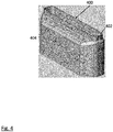
- solder nozzle 500 is shown, including solder outlet 502. As the nozzle 500 does not incorporate a de-bridging gas outlet, it may be generally similar to nozzle 104 of figure 1b , though no screen 106 is required. Nozzle 500, and particularly solder outlet 502, is shown exposed within opening 504 of cover plate 506. Cover plate 506 closes off the solder pot cavity as described above in connection with figure 1a , though only the portion surrounding opening 504 is shown in figures 5 and 6 . It will be appreciated that cover plate 506 may include further openings associated with further nozzles.
- Figures 5 and 6 further show a de-bridging gas outlet 508 in the form of an air knife with a single elongate gas outlet. It will be appreciated that alternatively two or more discrete gas openings may be provided.
- the de-bridging gas outlet 508 is 3D printed and secured to the cover plate 506 with screws 510. However, it will be appreciated firstly that 3D printing is only one suitable fabrication technique and secondly that alternative fixation techniques will be well known to the skilled person. Indeed, in some examples the de-bridging gas outlet 508 may be integrally formed with the cover plate 506 itself.
- de-bridging gas outlet 508 is directed towards the solder outlet 502 so that gas will be blown across parts of the PCB as they are lifted clear of the solder outlet 502, or moved downstream from the solder outlet 502 over the de-bridging gas outlet 508.
Priority Applications (3)
| Application Number | Priority Date | Filing Date | Title |
|---|---|---|---|
| US17/350,724 US20220009017A1 (en) | 2020-07-08 | 2021-06-17 | Soldering nozzle, system and use |
| MX2021007319A MX2021007319A (es) | 2020-07-08 | 2021-06-17 | Boquilla de soldadura, sistema y uso. |
| KR1020210086395A KR20220006465A (ko) | 2020-07-08 | 2021-07-01 | 납땜 노즐, 시스템 및 용도 |
Applications Claiming Priority (1)
| Application Number | Priority Date | Filing Date | Title |
|---|---|---|---|
| EP20184808 | 2020-07-08 |
Publications (1)
| Publication Number | Publication Date |
|---|---|
| EP3936271A1 true EP3936271A1 (de) | 2022-01-12 |
Family
ID=71728548
Family Applications (1)
| Application Number | Title | Priority Date | Filing Date |
|---|---|---|---|
| EP21169170.4A Pending EP3936271A1 (de) | 2020-07-08 | 2021-04-19 | Lötdüse, system und verwendung |
Country Status (4)
| Country | Link |
|---|---|
| US (1) | US20220009017A1 (de) |
| EP (1) | EP3936271A1 (de) |
| KR (1) | KR20220006465A (de) |
| MX (1) | MX2021007319A (de) |
Citations (6)
| Publication number | Priority date | Publication date | Assignee | Title |
|---|---|---|---|---|
| US20010030220A1 (en) * | 2000-03-09 | 2001-10-18 | Willis Scott E. | Apparatus and methods for wave soldering |
| EP1381487A1 (de) * | 2000-07-11 | 2004-01-21 | L'air Liquide, S.A. à Directoire et Conseil de Surveillance pour l'Etude et l'Exploitation des Procédés Georges Claude | Vorrichtung zur verbesserten inertisierung beim wellenlöten |
| US6913183B2 (en) * | 2002-09-30 | 2005-07-05 | Speedline Technologies, Inc. | Selective gas knife for wave soldering |
| US20170209949A1 (en) * | 2014-07-29 | 2017-07-27 | Illinois Tool Works Inc. | Soldering module |
| EP3785837A1 (de) * | 2019-08-27 | 2021-03-03 | Illinois Tool Works, Inc. | Düse, system und verfahren |
| EP3785838A1 (de) * | 2019-08-27 | 2021-03-03 | Illinois Tool Works, Inc. | Lötbaugruppe, verfahren und verwendung |
Family Cites Families (10)
| Publication number | Priority date | Publication date | Assignee | Title |
|---|---|---|---|---|
| US5065932A (en) * | 1990-09-24 | 1991-11-19 | International Business Machines Corporation | Solder placement nozzle with inert cover gas and inert gas bleed |
| US5397049A (en) * | 1991-12-06 | 1995-03-14 | Electrovert Ltd. | Gas shrouded solder wave with reduced solder splatter |
| US5292055A (en) * | 1991-12-06 | 1994-03-08 | Electrovert Ltd. | Gas shrouded wave improvement |
| US5240169A (en) * | 1991-12-06 | 1993-08-31 | Electrovert Ltd. | Gas shrouded wave soldering with gas knife |
| US5203489A (en) * | 1991-12-06 | 1993-04-20 | Electrovert Ltd. | Gas shrouded wave soldering |
| US6168065B1 (en) * | 1998-02-17 | 2001-01-02 | Soltec B.V. | Movable selective debridging apparatus for debridging soldered joints on printed circuit boards |
| US6164515A (en) * | 1998-02-17 | 2000-12-26 | Soltec B.V. | Movable selective debridging apparatus and method of debridging soldered joints on printed circuit boards using same |
| NL1024476C2 (nl) * | 2003-10-07 | 2005-04-08 | Vitronics Soltec B V | Inrichting voor selectief solderen. |
| DE102005052076B4 (de) * | 2005-10-28 | 2007-09-20 | Messer Group Gmbh | Lötvorrichtung mit Gasverteilung |
| CN104801809B (zh) * | 2014-01-29 | 2018-09-14 | 气体产品与化学公司 | 用于在焊接期间提供惰性气体的设备和方法 |
-
2021
- 2021-04-19 EP EP21169170.4A patent/EP3936271A1/de active Pending
- 2021-06-17 MX MX2021007319A patent/MX2021007319A/es unknown
- 2021-06-17 US US17/350,724 patent/US20220009017A1/en active Pending
- 2021-07-01 KR KR1020210086395A patent/KR20220006465A/ko unknown
Patent Citations (6)
| Publication number | Priority date | Publication date | Assignee | Title |
|---|---|---|---|---|
| US20010030220A1 (en) * | 2000-03-09 | 2001-10-18 | Willis Scott E. | Apparatus and methods for wave soldering |
| EP1381487A1 (de) * | 2000-07-11 | 2004-01-21 | L'air Liquide, S.A. à Directoire et Conseil de Surveillance pour l'Etude et l'Exploitation des Procédés Georges Claude | Vorrichtung zur verbesserten inertisierung beim wellenlöten |
| US6913183B2 (en) * | 2002-09-30 | 2005-07-05 | Speedline Technologies, Inc. | Selective gas knife for wave soldering |
| US20170209949A1 (en) * | 2014-07-29 | 2017-07-27 | Illinois Tool Works Inc. | Soldering module |
| EP3785837A1 (de) * | 2019-08-27 | 2021-03-03 | Illinois Tool Works, Inc. | Düse, system und verfahren |
| EP3785838A1 (de) * | 2019-08-27 | 2021-03-03 | Illinois Tool Works, Inc. | Lötbaugruppe, verfahren und verwendung |
Also Published As
| Publication number | Publication date |
|---|---|
| MX2021007319A (es) | 2022-01-10 |
| KR20220006465A (ko) | 2022-01-17 |
| US20220009017A1 (en) | 2022-01-13 |
Similar Documents
| Publication | Publication Date | Title |
|---|---|---|
| US5656139A (en) | Electroplating apparatus | |
| US6655574B2 (en) | Apparatus for selective soldering | |
| EP0337149B1 (de) | Lötmittelauftragegerät | |
| US11845226B2 (en) | Additive manufacturing nozzle and additive manufacturing device | |
| JP6619019B2 (ja) | 対基板作業システム、および挿入方法 | |
| US20210060676A1 (en) | Soldering assembly, method and use | |
| JPH08507254A (ja) | ガスナイフジェットを備えるはんだノズル | |
| WO2007069705A1 (en) | Apparatus and method for soldering flat work piece | |
| JP2017092222A (ja) | 半田付け装置、および半田付け方法 | |
| CN107251666B (zh) | 钎焊装置 | |
| CN109565938B (zh) | 钎焊装置 | |
| WO2017002187A1 (ja) | 対基板作業機、および認識方法 | |
| EP3936271A1 (de) | Lötdüse, system und verwendung | |
| EP0478170B1 (de) | Aufbringen einer Lötpaste | |
| JP4012515B2 (ja) | はんだ付け方法およびはんだ付け装置 | |
| CN112439967A (zh) | 喷嘴、系统和方法 | |
| JP4724669B2 (ja) | フローディップはんだ付け装置 | |
| JPS6315063B2 (de) | ||
| KR102191293B1 (ko) | 3d 프린터를 이용한 전자 복합 제조 장치 및 그 방법 | |
| JP2017087261A (ja) | 半田付け装置、半田付け方法、および半田マガジン | |
| JP2007053165A (ja) | ハンダ付け装置 | |
| JP2000223827A (ja) | 噴流式局所はんだ付け装置 | |
| JP6531453B2 (ja) | はんだ付け装置およびそれを用いた被はんだ付け対象物の製造方法 | |
| JP2001347366A (ja) | 局所はんだ付け装置 | |
| CN113365437B (zh) | 控制器生产用电路板焊锡装置 |
Legal Events
| Date | Code | Title | Description |
|---|---|---|---|
| PUAI | Public reference made under article 153(3) epc to a published international application that has entered the european phase |
Free format text: ORIGINAL CODE: 0009012 |
|
| STAA | Information on the status of an ep patent application or granted ep patent |
Free format text: STATUS: THE APPLICATION HAS BEEN PUBLISHED |
|
| AK | Designated contracting states |
Kind code of ref document: A1 Designated state(s): AL AT BE BG CH CY CZ DE DK EE ES FI FR GB GR HR HU IE IS IT LI LT LU LV MC MK MT NL NO PL PT RO RS SE SI SK SM TR |
|
| B565 | Issuance of search results under rule 164(2) epc |
Effective date: 20210924 |
|
| STAA | Information on the status of an ep patent application or granted ep patent |
Free format text: STATUS: REQUEST FOR EXAMINATION WAS MADE |
|
| 17P | Request for examination filed |
Effective date: 20220524 |
|
| RBV | Designated contracting states (corrected) |
Designated state(s): AL AT BE BG CH CY CZ DE DK EE ES FI FR GB GR HR HU IE IS IT LI LT LU LV MC MK MT NL NO PL PT RO RS SE SI SK SM TR |
|
| STAA | Information on the status of an ep patent application or granted ep patent |
Free format text: STATUS: EXAMINATION IS IN PROGRESS |
|
| 17Q | First examination report despatched |
Effective date: 20230531 |