EP3926331B1 - Electronic component inspection method - Google Patents
Electronic component inspection method Download PDFInfo
- Publication number
- EP3926331B1 EP3926331B1 EP21180064.4A EP21180064A EP3926331B1 EP 3926331 B1 EP3926331 B1 EP 3926331B1 EP 21180064 A EP21180064 A EP 21180064A EP 3926331 B1 EP3926331 B1 EP 3926331B1
- Authority
- EP
- European Patent Office
- Prior art keywords
- electronic component
- image
- image capture
- light
- terminals
- Prior art date
- Legal status (The legal status is an assumption and is not a legal conclusion. Google has not performed a legal analysis and makes no representation as to the accuracy of the status listed.)
- Active
Links
Images


Classifications
-
- G—PHYSICS
- G01—MEASURING; TESTING
- G01B—MEASURING LENGTH, THICKNESS OR SIMILAR LINEAR DIMENSIONS; MEASURING ANGLES; MEASURING AREAS; MEASURING IRREGULARITIES OF SURFACES OR CONTOURS
- G01B11/00—Measuring arrangements characterised by the use of optical techniques
- G01B11/02—Measuring arrangements characterised by the use of optical techniques for measuring length, width or thickness
- G01B11/06—Measuring arrangements characterised by the use of optical techniques for measuring length, width or thickness for measuring thickness ; e.g. of sheet material
- G01B11/0608—Height gauges
-
- G—PHYSICS
- G01—MEASURING; TESTING
- G01N—INVESTIGATING OR ANALYSING MATERIALS BY DETERMINING THEIR CHEMICAL OR PHYSICAL PROPERTIES
- G01N21/00—Investigating or analysing materials by the use of optical means, i.e. using sub-millimetre waves, infrared, visible or ultraviolet light
- G01N21/84—Systems specially adapted for particular applications
- G01N21/88—Investigating the presence of flaws or contamination
- G01N21/95—Investigating the presence of flaws or contamination characterised by the material or shape of the object to be examined
- G01N21/956—Inspecting patterns on the surface of objects
- G01N21/95684—Patterns showing highly reflecting parts, e.g. metallic elements
-
- G—PHYSICS
- G01—MEASURING; TESTING
- G01N—INVESTIGATING OR ANALYSING MATERIALS BY DETERMINING THEIR CHEMICAL OR PHYSICAL PROPERTIES
- G01N21/00—Investigating or analysing materials by the use of optical means, i.e. using sub-millimetre waves, infrared, visible or ultraviolet light
- G01N21/84—Systems specially adapted for particular applications
- G01N21/88—Investigating the presence of flaws or contamination
- G01N21/8806—Specially adapted optical and illumination features
-
- G—PHYSICS
- G02—OPTICS
- G02B—OPTICAL ELEMENTS, SYSTEMS OR APPARATUS
- G02B26/00—Optical devices or arrangements for the control of light using movable or deformable optical elements
- G02B26/08—Optical devices or arrangements for the control of light using movable or deformable optical elements for controlling the direction of light
- G02B26/0816—Optical devices or arrangements for the control of light using movable or deformable optical elements for controlling the direction of light by means of one or more reflecting elements
-
- H—ELECTRICITY
- H04—ELECTRIC COMMUNICATION TECHNIQUE
- H04N—PICTORIAL COMMUNICATION, e.g. TELEVISION
- H04N23/00—Cameras or camera modules comprising electronic image sensors; Control thereof
- H04N23/56—Cameras or camera modules comprising electronic image sensors; Control thereof provided with illuminating means
-
- G—PHYSICS
- G01—MEASURING; TESTING
- G01N—INVESTIGATING OR ANALYSING MATERIALS BY DETERMINING THEIR CHEMICAL OR PHYSICAL PROPERTIES
- G01N2201/00—Features of devices classified in G01N21/00
- G01N2201/06—Illumination; Optics
- G01N2201/063—Illuminating optical parts
- G01N2201/0636—Reflectors
Definitions
- the present disclosure relates to an electronic component inspection method.
- Pre-shipment inspection of manufactured electronic component is a usual practice at manufacturing sites of electronic component.
- Known apparatus for inspecting electronic component is exemplified by an appearance inspection apparatus described in JP-H10-288508A .
- the apparatus described in JP-H10-288508A has an integrated structure of a two-dimensional image lighting unit, a camera for capturing a two-dimensional image illuminated by the two-dimensional image lighting unit, a laser irradiation unit that irradiates laser light on an object, and a laser spot receiving position detector that receives laser light reflected on the object to determine change of height level of the object, thereby enabling acquisition of a two-dimensional image and a three-dimensional height information at a time.
- Document EP 0 425 722 A1 shows an arrangement for detecting the position of connecting pins of electronic components by positioning the electronic components at least approximately on a translucent, light-scattering plate with simultaneous illumination of the connecting pins and evaluation of the shape of the shading generated on the transparent plate through the connecting pins by means of an image recording on the side of the transparent plate opposite the electronic component with connected image processing. At least one light source for sequential Illumination of the connecting pins from two different directions.
- the method comprises illuminating the device edge and leads with backlit diffuse illumination radiating in the directions corresponding to the first and second optical axes, capturing a first backlit image of the device edge and the leads in a direction corresponding to the first optical axis, deflecting a second backlit image of the device edge and leads from a direction corresponding to the second optical axis into a direction corresponding to the first optical axis, and capturing the second deflected backlit image of the device edge and the leads.
- a method for obtaining a machine-vision image of an object comprising blocking a first portion of the object with a first illuminated surface, and imaging a second portion of the object using back light from the first illuminated surface.
- Inspection of electronic component include inspection of mounting failure.
- the mounting failure is judged on the basis of inclination (flatness) of a component body when mounted on a board.
- the flatness of the electronic component is detected by measuring height of a terminal that extends out from the component body of the electronic component, that is, the height of terminal with reference to the component body. The more precisely the height of terminal is measured, the more precisely the mounting failure is detectable.
- the height of terminal is determined on an image of the terminal captured with a camera.
- a possible way to detect the height of terminal may be such as applying the appearance inspection apparatus described in JP-H10-288508A , and obtaining information regarding the height of terminal from the two-dimensional image.
- the present disclosure conceived considering the aforementioned problem, is to provide an inspection method capable of accurately specifying an inspection point on the terminal of the electronic component.
- an electronic component inspection method in accordance with claim 1 is provided.
- Advantageous embodiments of this aspect are defined in dependent claims 2 to 4
- the present disclosure can provide an electronic component inspection method that can accurately specify an inspection point on a terminal of an electronic component.
- FIG. 1 is a perspective view illustrating an electronic component 1 to be inspected by using an electronic component inspection apparatus suitable for carrying out the method in accordance with the present embodiments, in which the electronic component 1 is viewed from the side facing to the mounting face.
- the "mounting face” in the context of this patent specification is a virtual plane assumed when the electronic component 1 is mounted.
- Figs. 2A and 2B are drawings illustrating the top face and the bottom face (the bottom face will also be denoted as "terminal face”, hereinafter), wherein Fig. 2A is a bottom view of the electronic component 1, and Fig. 2B is a top view of the electronic component 1.
- the electronic component 1 has a component body 10 and terminals 11, 12. Note that terminals 111, 122 that extend from the component body 10 are entwined terminals, and are not constituents of the mounting terminal.
- the component body 10 has a bobbin (not illustrated) with a wound part (not illustrated) around which a coil 15 is wound on the outer circumference thereof, a base 16 that houses the bobbin, and outside legs 17 that partially house the terminals 11, 12 and partially allow them to expose.
- the terminals 11, 12 are mounting terminals that are electrically connected respectively with the terminals 111, 122 to which coil ends (not illustrated) of the coil 15 are entwined, and are mounted on an unillustrated mounting board. These plurality of terminals 11, 12 are held in parallel to each other by the base 16.
- a face which is directed opposite to the mounting face when the electronic component 1 is mounted will be denoted as a "back face”. That is, the back face in the context of the present embodiments is determined with reference to the mounting face. The back face is identical to the top face of the electronic component 1.
- the terminals 11, 12 are lead terminals that extend from the component body 10 in mutually opposite directions.
- the terminal that extends from the base 16 leftwards in Figs. 2A and 2B is referred to as the terminal 11, and the terminal that extends rightwards is referred to as the terminal 12 for convenience.
- the present embodiments are not limited to inspection of the lead terminals, and instead are also applicable to any types of electronic component in which a part of the component body 10 and parts of the terminals 11, 12 form an overlapping area when viewed from the side of the mounting face.
- the light is irradiated on the electronic component 1 from the side of the back face, to acquire a two-dimensional image of the back face.
- Contour shapes of the terminals 11, 12 are then detected from the thus obtained two-dimensional image, and points (ordinates) on the terminals 11, 12 are detected referring to edges of the terminals 11, 12 determined on the basis of the contour shapes. Processing is then carried out to correlate the thus detected points with predetermined inspection points.
- the first embodiment is devised to insert a reflective plate into an overlapping areas of each of the terminals 11, 12 and the component body 10 when viewed from the side of the mounting face, so as to allow the irradiation light to reflect thereon, to thereby capture an image (referred to as "backlit image”, hereinafter) showing sharp edges of the terminals 11, 12.
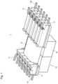
- Fig. 3 is a drawing explaining an electronic component inspection apparatus suitable for carrying out the method in accordance with the first embodiment (also simply referred to as "inspection apparatus", hereinafter), and is a top view of an inspection apparatus 100.
- the inspection apparatus 100 has a holder 20 that holds and fixes the electronic component 1.
- Fig. 3 is a drawing of the inspection apparatus 100 viewed from the side of the mounting face of the electronic component 1.
- the inspection apparatus 100 has a pair of reflective plates 21, 22 arranged while placing in between an image capture area A in which the electronic component 1 is shot.
- the image capture area A corresponds to a zone shot by a camera 25 illustrated in Fig. 4 .
- the electronic component 1, when shot, is held and fixed so that the terminal face confronts the camera 25 and falls within the image capture area A.
- the reflective plates 21, 22 are arranged one by one laterally on both sides of the image capture area A, each of which being inserted into an area where the component body 10 overlaps with the terminal 11 or with the terminal 12.
- the reflective plates 21, 22 have the ends thereof slightly declined towards the virtual mounting plane assumed when the electronic component 1 is mounted. Tilt of the reflective plates will be described later referring to Fig. 4 and other drawings.
- the reflective plates 21, 22 have formed therein long holes 102, and are fixed to an unillustrated base with use of bolts 101 inserted in the long holes 102.
- the inspection apparatus 100 further has a transfer unit that transfers the electronic component 1.
- the transfer unit may have any structure not specifically limited, by which the electronic component 1 may be loaded typically with use of a robot arm into the image capture area A from the front of the sheet of Fig. 3 , or may alternatively be transferred in the vertical direction of Fig. 3 typically with use of a belt conveyor, so as to move sequentially into the image capture area A, and then leave the image capture area A after shot.
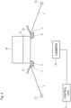
- Fig. 4 is a schematic drawing for explaining the inspection apparatus suitable for carrying out the method in accordance with the first embodiment.
- the inspection apparatus has the holder that holds the electronic component 1 having the terminals 11, 12 at a predetermined position; and a photo-irradiation unit that irradiates reflected light Lr at least onto the terminals 11, 12 of the electronic component 1 held by the holder 20, from the back face.
- the photo-irradiation unit in the first embodiment has light sources 31, 32 and the reflective plates 21, 22. A part of irradiation light L emitted from the light sources 31, 32 is reflected on the reflective plates 21, 22, and irradiated as the reflected light Lr onto the terminals 11, 12 from the back face.
- the structure illustrated in Fig. 4 also has the camera 25, which is an image capture unit that captures an image of the electronic component 1 being irradiated by the irradiation light L and the reflected light Lr with use of the light sources 31, 32 and the reflective plates 21, 22; and a control unit 5 that controls processing related to inspection of the electronic component 1, on the basis of the image of the electronic component 1 captured by the camera 25.
- the reflected light Lr is given as backlight for shooting the terminals 11, 12, when viewed from the camera 25.
- the first embodiment although illustrated in Fig. 4 as an exemplary case having the light sources 31, 32 and the camera 25 arranged below the electronic component 1, is not limited to such structure.
- the first embodiment may alternatively be devised to set the electronic component 1 with the terminal face directed upward, and to arrange the light sources 31, 32 and the camera 25 above the electronic component 1 so as to shoot the terminal face.
- the first embodiment can brighten the terminal face, and can obtain a sharp image of the terminals 11, 12. Such case would, however, make the light scattered on the edges of the terminals, occasionally making the edge contour less discriminable on the image.
- the irradiation light L would be shadowed by the component body 10, so as to make the area where the terminals 11, 12 and the component body 10 overlap less recognizable on the image.
- the present inventors of the present disclosure presupposed that the level of height of the terminals 11, 12 is measured at a plurality of inspection points, so that the aforementioned situation would fail in achieving accuracy sufficient for determining the measuring points of the height level of the terminals 11, 12.
- the first embodiment is devised to compose the photo-irradiation unit by using the light sources 31, 32 that irradiate irradiation light L onto the electronic component; and the reflective plates 21, 22 which serve as a reflector on which the irradiation light L emitted from the light sources 31, 32 is reflect towards the terminals 11, 12, as described above.
- the light sources 31, 32 are freely selectable for example from known types of lamp and light emitting diode (LED).
- the reflective plates 21, 22 are preferably made of a highly reflective material, such as aluminum, stainless steel and other metals. A part of the irradiation light L directed towards the terminals 11, 12 is converted to the reflected light Lr on the reflective plates 21, 22, and then irradiated on the terminals 11, 12 from the back face.
- the reflective plates 21, 22 are inserted so as to respectively aim at kinks between the downwardly protruded sections and the outwardly protruded sections of the terminals 11, 12.
- the reflective plates 21, 22 in this setting are inclined downwards to the mounting face of the electronic component 1.
- the reflective plates 21, 22 are, however, not always necessarily be angled in this way, instead may be nearly in parallel with the mounting face, or may be inclined upwards from the mounting face. Angles of the reflective plates 21, 22 are suitably determined so as to enhance intensity of the reflected light at a desired position, typically depending on distance between the component body 10 and the terminals 11, 12, depth of the overlapping area, and position of the inspection points.
- the contour shape is detectable by any of known techniques of edge detection in image processing.
- the edge detection may rely entirely upon the control unit 5, or may rely partly upon an operator of the inspection apparatus.
- the edge detection in this case may be such that the control unit 5 detects the edges of the terminals 11, 12, and presents them to the operator. The operator then may enter information for adjusting or correcting the edges, detected by the control unit 5, through an unillustrated input device into the control unit 5.
- the inspection points may be set, for example, automatically by the control unit 5 according to predetermined conditions. Such processing may be accomplished typically by, as illustrated in Fig. 5 , determining on the image the inspection point p0 on the edge of the terminal 12, and assuming this point as the origin, by setting pixels that are distant away from the origin by predetermined numbers of pixels in the x-direction and y-direction, as candidates for the inspection points p1 to p8.
- the control unit 5 may alternatively determine, from among the thus determined candidates for the inspection points p1 to p8, at least a part thereof according to a predetermined number or layout of the inspection points.
- a part of the lead terminals 11, 12 and a part of the component body 10 are arranged apart from each other, and so as to form an overlapping area when viewed from the side of the mounting face and the method further comprises: inserting a reflective plate 21, 22 into the overlapping area of the component body 10 and the lead terminal 11, 12 at a level of height between the component body 10 and the lead terminals 11 and 12, irradiating irradiation light L emitted from the light source 31, 32 on the terminal face of the lead terminals 11 and 12, reflecting, from the side of the back face, the irradiation light L on the reflective plate 21, 22 so as to convert the irradiation light L to the reflected light Lr, and irradiating the reflected light Lr on at least the lead terminals 11, 12 from the side of the back face.
- the step of irradiating the irradiation light L and the reflected light Lr is conducted while holding and fixing the electronic component 1.
- Action of making the holder hold the electronic component 1 may be assisted by some device such as robot arm, or may be manually achieved by the operator.
- the irradiation light L may be irradiated, for example, with the aid of the control unit 5, or a device that controls any unillustrated mechanism. Use of the control unit 5 for irradiation of the irradiation light L will, however, facilitate the first embodiment to synchronize irradiation timing of the irradiation light L and acquisition timing of image data.
- the irradiation light L may alternatively be irradiated manually by the operator who switches ON the light sources 31, 32 which are the light sources of laser light.
- the step of capturing an image of the electronic component 1 under of the irradiation light L and the reflected light Lr may be activated, when the control unit 5 outputs a control signal that notifies shooting timing towards the control unit 5. Note, however, that shooting per se may be conducted by the operator through handling of the camera 25.
- the aforementioned processing may be followed by measurement of the distance between the camera 25 and the terminals 11, 12. Height may be measured with use of a 3D camera, typically according to the time-of-flight (TOF) system.
- TOF time-of-flight
- the camera 25 is preferably the 3D camera.
- the thus measured distance is then computed to determine flatness of the electronic component 1 when mounted, making it possible to judge whether the electronic component 1 is acceptable or rejected.
- a backlit image with sharp edges is obtainable since the reflected light Lr is irradiated on the back face of the terminals 11, 12.
- the electronic component inspection apparatus suitable for carrying out the method in accordance with the first embodiment and the electronic component inspection method of the first embodiment can therefore accurately determine the inspection points on the terminals of the electronic component.
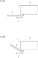
- the angle changer makes change so that the angle of the reflective plates relative to the mounting face, during image capture of the electronic component within the image capture area A (a predetermined tilt angle as illustrated in Fig. 6B ), so as to become larger than the angle of the reflective plates relative to the mounting face, during transfer of the electronic component from the outside to the inside, or from the inside to the outside, of the image capture area A (nearly flat angle as illustrated in 6A).
- the second embodiment now becomes possible to reduce a range occupied heightwise by the reflective plates 21, 22 in the overlapping area between the component body 10 and the terminal 11, upon completion of shooting of the electronic component 1 and exit from the image capture area A, and can prevent the electronic component 1, when transferred, from interfering with the reflective plate 21.
- the reflective plates 21, 22 during shooting are tilted between the component body 10 and the terminal 11. In this way, the light that was emitted from the light sources 31, 32 obliquely towards the component body 10, and was converted into the reflected light Lr after incident on the lower faces of the reflective palates 21, 22 can now illuminate the terminals 11, 12 nearly perpendicularly as illustrated in Fig. 4 , making it possible to efficiently condense the reflected light Lr onto the terminals 11, 12.
- Figs. 7A and 7B are drawings for explaining a variation 1 of the second embodiment.
- the inspection apparatus suitable for carrying out the method in accordance with variation 1 further has a reflective plate shifter that shifts the reflective plates 21, 22 closer to or away from the electronic component 1.
- the reflective plate shifter shifts the reflective plates 21, 22 so that they will become distant from the electronic component 1 outwardly in the direction the terminals 11, 12 extend, more largely during transfer of the electric component 1, than during image capture of the electronic component 1.
- the control unit 5 functions as the reflective plate shifter.
- the control unit 5 shifts the reflective plates 21, 22 so as to make them closer to the electronic component 1 during image capture of the electronic component 1, and to make them more distant from the electronic component 1 after the image capture.
- Fig. 7A illustrates a position of the reflective plate 21 during the image capture
- Fig. 7B illustrates a position of the reflective plate 21 retracted from the electronic component 1 after the image capture.
- This motion of the reflective plates 21, 22 may be enabled by providing an unillustrated drive unit, typically a stepping motor, that brings the reflective plates 21, 22 away from or closer to the electronic component 1, wherein towards a driver of the drive unit, the control unit 5 outputs a control signal that instructs the drive operation.
- the control unit 5 Upon acquisition of image data of a preceding electronic component 1, the control unit 5 outputs a control signal that instructs retraction of the reflective plates 21, 22, from the position illustrated in Fig. 7A to the position illustrated in Fig. 7B , towards the drive unit of the reflective plates 21, 22.
- the drive unit retracts the reflective plate 21 from end point position M0 to position M1 where the reflective plate 21, when viewed from the mounting face, will not overlap the terminals 11, 12.
- reflective plate 21 is consequently retracted by distance ⁇ M from position M0.
- the electronic component 1 is successfully prevented from interfering with the reflective plates 21, 22, when a transfer unit (not illustrated) of the inspection apparatus transfers the electronic component 1 in whichever direction from among the vertical and depth directions of Fig. 7B .
- the structure suitable for carrying out the method in accordance with the second embodiment, aimed to avoid interference of the electric component 1 and the reflective plates 21, 22, is not limited to those relying upon driving of the reflective plates 21, 22.
- Fig. 8 a drawing for explaining the inspection apparatus suitable for carrying out the method in accordance with a variation 2 of the second embodiment.
- the reflective plates 21, 22 as the reflector are fixed in an area that does not overlap the electronic component 1 when viewed from the side of the mounting face.
- an area that overlaps the electronic component is denoted by I, and the area that does not overlap is denoted by O.
- the entire ranges of the reflective plates 21, 22 including the ends are fixed within the area O.
- the reflective plates 21, 22 are arranged with the ends thereof obliquely declined towards the component body 10. In this way, the reflective plates 21, 22, even if being thus fixed, will no longer interfere with the electronic component 1, making it possible to reduce nonconformities such that the apparatus is interrupted during inspection of the electronic component, or such that the terminals 11, 12 of the electronic component 1 are damaged.
Landscapes
- Physics & Mathematics (AREA)
- General Physics & Mathematics (AREA)
- Health & Medical Sciences (AREA)
- Life Sciences & Earth Sciences (AREA)
- Chemical & Material Sciences (AREA)
- Analytical Chemistry (AREA)
- Biochemistry (AREA)
- General Health & Medical Sciences (AREA)
- Immunology (AREA)
- Pathology (AREA)
- Optics & Photonics (AREA)
- Engineering & Computer Science (AREA)
- Multimedia (AREA)
- Signal Processing (AREA)
- Investigating Materials By The Use Of Optical Means Adapted For Particular Applications (AREA)
- Supply And Installment Of Electrical Components (AREA)
Description
- The present disclosure relates to an electronic component inspection method.
- Pre-shipment inspection of manufactured electronic component is a usual practice at manufacturing sites of electronic component. Known apparatus for inspecting electronic component is exemplified by an appearance inspection apparatus described in
JP-H10-288508A JP-H10-288508A - Document
EP 0 425 722 A1 shows an arrangement for detecting the position of connecting pins of electronic components by positioning the electronic components at least approximately on a translucent, light-scattering plate with simultaneous illumination of the connecting pins and evaluation of the shape of the shading generated on the transparent plate through the connecting pins by means of an image recording on the side of the transparent plate opposite the electronic component with connected image processing. At least one light source for sequential Illumination of the connecting pins from two different directions. - In document
WO 2002/044651 A1 , a method for providing first and second backlit images of a semiconductor device edge and leads extending therefrom, is shown, wherein these images represent first and second viewing angles corresponding to first and second different optical axes as measured in a plate perpendicular to the device edge. The method comprises illuminating the device edge and leads with backlit diffuse illumination radiating in the directions corresponding to the first and second optical axes, capturing a first backlit image of the device edge and the leads in a direction corresponding to the first optical axis, deflecting a second backlit image of the device edge and leads from a direction corresponding to the second optical axis into a direction corresponding to the first optical axis, and capturing the second deflected backlit image of the device edge and the leads. - According to document
US 2003/0174318 A1 , a method for obtaining a machine-vision image of an object is known, the method comprising blocking a first portion of the object with a first illuminated surface, and imaging a second portion of the object using back light from the first illuminated surface. - Inspection of electronic component include inspection of mounting failure. The mounting failure is judged on the basis of inclination (flatness) of a component body when mounted on a board. The flatness of the electronic component is detected by measuring height of a terminal that extends out from the component body of the electronic component, that is, the height of terminal with reference to the component body. The more precisely the height of terminal is measured, the more precisely the mounting failure is detectable.
- The height of terminal is determined on an image of the terminal captured with a camera. Hence, a possible way to detect the height of terminal may be such as applying the appearance inspection apparatus described in
JP-H10-288508A - In a case of detecting the height of terminal which extends out from the bottom face of body of the electronic component, an effort for obtaining a sharp image by irradiating light from the side of a mounting face of the terminal, as described in
JP-H10-288508A - The present disclosure, conceived considering the aforementioned problem, is to provide an inspection method capable of accurately specifying an inspection point on the terminal of the electronic component. In an aspect of the present invention, an electronic component inspection method in accordance with
claim 1 is provided. Advantageous embodiments of this aspect are defined in dependent claims 2 to 4 - The present disclosure can provide an electronic component inspection method that can accurately specify an inspection point on a terminal of an electronic component.
-
-
Fig. 1 is a perspective view illustrating an electronic component to be inspected by using an electronic component inspection apparatus suitable for carrying out the method of an aspect of the invention; -
Fig. 2A is a bottom view of the electronic component illustrated inFig. 1 , andFig. 2B is a top view; -
Fig. 3 is a top view illustrating an electronic component inspection apparatus suitable for carrying out the method in accordance with a first embodiment; -
Fig. 4 is a schematic drawing illustrating the electronic component inspection apparatus of the first embodiment; -
Fig. 5 is a schematic drawing illustrating a captured image of a terminal; -
Figs. 6A and 6B are drawings illustrating an electronic component inspection apparatus suitable for carrying out the method in accordance with a second embodiment, whereinFig. 6A illustrates a reflective plate during transfer of the electronic component, andFig. 6B illustrates the reflective plate during image capture of the electronic component; -
Figs. 7A and 7B are drawings illustrating avariation 1 of the second embodiment, whereinFig. 7A illustrates a position of the reflective plate during image capture, andFig. 7B illustrates a position of the reflective plate shifted apart from the image capture area after image capture; and -
Fig. 8 is a drawing explaining an electronic component inspection apparatus suitable for carrying out the method of an aspect of the invention according to a variation 2 of the second embodiment. - Prior to explanation of embodiments of the present disclosure, a first embodiment and a second embodiment of the present disclosure (also collectively referred to as "the present embodiments", hereinafter) will be outlined.
Fig. 1 is a perspective view illustrating anelectronic component 1 to be inspected by using an electronic component inspection apparatus suitable for carrying out the method in accordance with the present embodiments, in which theelectronic component 1 is viewed from the side facing to the mounting face. Note now that the "mounting face" in the context of this patent specification is a virtual plane assumed when theelectronic component 1 is mounted. -
Figs. 2A and 2B are drawings illustrating the top face and the bottom face (the bottom face will also be denoted as "terminal face", hereinafter), whereinFig. 2A is a bottom view of theelectronic component 1, andFig. 2B is a top view of theelectronic component 1. Theelectronic component 1 has acomponent body 10 andterminals terminals component body 10 are entwined terminals, and are not constituents of the mounting terminal. - The
component body 10 has a bobbin (not illustrated) with a wound part (not illustrated) around which acoil 15 is wound on the outer circumference thereof, abase 16 that houses the bobbin, andoutside legs 17 that partially house theterminals terminals terminals coil 15 are entwined, and are mounted on an unillustrated mounting board. These plurality ofterminals base 16. - In the present disclosure, a face which is directed opposite to the mounting face when the
electronic component 1 is mounted will be denoted as a "back face". That is, the back face in the context of the present embodiments is determined with reference to the mounting face. The back face is identical to the top face of theelectronic component 1. - The
terminals component body 10 in mutually opposite directions. In the present embodiments, the terminal that extends from thebase 16 leftwards inFigs. 2A and 2B is referred to as theterminal 11, and the terminal that extends rightwards is referred to as theterminal 12 for convenience. Note, however, that the present embodiments are not limited to inspection of the lead terminals, and instead are also applicable to any types of electronic component in which a part of thecomponent body 10 and parts of theterminals - When using the electronic component inspection apparatus suitable for carrying out the method in accordance with the first embodiment, the light is irradiated on the
electronic component 1 from the side of the back face, to acquire a two-dimensional image of the back face. Contour shapes of theterminals terminals terminals - In the processing, the irradiation light irradiated on the back face of the
terminals terminals component body 10. Aiming at solving this problem, the first embodiment is devised to insert a reflective plate into an overlapping areas of each of theterminals component body 10 when viewed from the side of the mounting face, so as to allow the irradiation light to reflect thereon, to thereby capture an image (referred to as "backlit image", hereinafter) showing sharp edges of theterminals - The first embodiment of the present disclosure will be explained below, referring to the drawings. Note that the drawings are merely illustrative ones for explaining structures, arrangements and functions of an exemplary electronic component inspection apparatus suitable for carrying out the method in accordance with the first embodiment, without limiting specific shapes and other features. In all drawings, all similar components are given the same reference signs, for the convenience of occasionally skipping a part of explanations.
-
Fig. 3 is a drawing explaining an electronic component inspection apparatus suitable for carrying out the method in accordance with the first embodiment (also simply referred to as "inspection apparatus", hereinafter), and is a top view of aninspection apparatus 100. Theinspection apparatus 100 has aholder 20 that holds and fixes theelectronic component 1.Fig. 3 is a drawing of theinspection apparatus 100 viewed from the side of the mounting face of theelectronic component 1. - The
inspection apparatus 100 has a pair ofreflective plates electronic component 1 is shot. The image capture area A corresponds to a zone shot by acamera 25 illustrated inFig. 4 . Theelectronic component 1, when shot, is held and fixed so that the terminal face confronts thecamera 25 and falls within the image capture area A. Thereflective plates component body 10 overlaps with the terminal 11 or with the terminal 12. Thereflective plates electronic component 1 is mounted. Tilt of the reflective plates will be described later referring toFig. 4 and other drawings. - The
reflective plates long holes 102, and are fixed to an unillustrated base with use ofbolts 101 inserted in thelong holes 102. Theinspection apparatus 100 further has a transfer unit that transfers theelectronic component 1. The transfer unit may have any structure not specifically limited, by which theelectronic component 1 may be loaded typically with use of a robot arm into the image capture area A from the front of the sheet ofFig. 3 , or may alternatively be transferred in the vertical direction ofFig. 3 typically with use of a belt conveyor, so as to move sequentially into the image capture area A, and then leave the image capture area A after shot. - The
holder 20 holds theterminals terminals terminals electronic component 1.Fig. 4 is a schematic drawing for explaining the inspection apparatus suitable for carrying out the method in accordance with the first embodiment. As illustrated inFig. 4 , the inspection apparatus has the holder that holds theelectronic component 1 having theterminals terminals electronic component 1 held by theholder 20, from the back face. The photo-irradiation unit in the first embodiment haslight sources reflective plates light sources reflective plates terminals - The structure illustrated in
Fig. 4 also has thecamera 25, which is an image capture unit that captures an image of theelectronic component 1 being irradiated by the irradiation light L and the reflected light Lr with use of thelight sources reflective plates electronic component 1, on the basis of the image of theelectronic component 1 captured by thecamera 25. The reflected light Lr is given as backlight for shooting theterminals camera 25. - Note that the first embodiment, although illustrated in
Fig. 4 as an exemplary case having thelight sources camera 25 arranged below theelectronic component 1, is not limited to such structure. The first embodiment may alternatively be devised to set theelectronic component 1 with the terminal face directed upward, and to arrange thelight sources camera 25 above theelectronic component 1 so as to shoot the terminal face. - With the irradiation light L irradiated on the terminal face of the
electronic component 1, the first embodiment can brighten the terminal face, and can obtain a sharp image of theterminals component body 10, so as to make the area where theterminals component body 10 overlap less recognizable on the image. The present inventors of the present disclosure presupposed that the level of height of theterminals terminals - Aimed at solving this problem, the first embodiment is devised to compose the photo-irradiation unit by using the
light sources reflective plates light sources terminals light sources reflective plates terminals reflective plates terminals - As described previously, the
electronic component 1 has the lead terminals that extend out from thecomponent body 10. A part of the lead terminals and a part of thecomponent body 10 are arranged apart from each other, and form an overlapping area when viewed from the side of the mounting face. Thereflective plates component body 10 and theterminals terminals component body 10, and further outwards again from thecomponent body 10. In the exemplary case illustrated inFig. 4 , downwardly protruded sections and outwardly protruded sections of theterminals component body 10. - In the exemplary case illustrated in
Fig. 4 , thereflective plates terminals reflective plates electronic component 1. Thereflective plates reflective plates component body 10 and theterminals - Positions and distances of the
light sources reflective plates terminals - The
camera 25 shoots a range that covers theterminals electronic component 1.Fig. 5 is a schematic drawing for explaining a captured image of the terminal 12. With the reflected light Lr reflected on thereflective plate 22 and irradiated on the terminal 12 from the back face, the terminal 12 looks dark on the image, while the periphery of the terminal 12 looks bright. On such image, brightness at the boundary between the terminal 12 and the background largely changes, sharply depicting the edge of the terminal 12. - The control unit 5 acquires data of the image (image data) shot by the
camera 25. On the basis of the image of theelectronic component 1, the control unit 5 detects contour shapes of at least theterminals camera 25 is a backlit image in which brightness changes largely between theterminals terminals Fig. 5 ) are set, on the basis of the contour shape detected by the control unit 5. - The contour shape is detectable by any of known techniques of edge detection in image processing. In the first embodiment, the edge detection may rely entirely upon the control unit 5, or may rely partly upon an operator of the inspection apparatus. The edge detection in this case may be such that the control unit 5 detects the edges of the
terminals - The inspection points may be set, for example, automatically by the control unit 5 according to predetermined conditions. Such processing may be accomplished typically by, as illustrated in
Fig. 5 , determining on the image the inspection point p0 on the edge of the terminal 12, and assuming this point as the origin, by setting pixels that are distant away from the origin by predetermined numbers of pixels in the x-direction and y-direction, as candidates for the inspection points p1 to p8. The control unit 5 may alternatively determine, from among the thus determined candidates for the inspection points p1 to p8, at least a part thereof according to a predetermined number or layout of the inspection points. - Also in such processing, a part of procedures may be left in charge of the operator. Procedures left in charge of the operator are exemplified by fine adjustment or selection of the inspection points.
- As can be understood from the description above, the inspection method of the first embodiment includes: irradiating the reflected light Lr on at least the
terminals electronic component 1 that has acomponent body 10 and theterminals electronic component 1; capturing an image of the electronic component under irradiation of the reflected light Lr; and controlling processing related to inspection of the electronic component, on the basis of the captured image of the electronic component. Herein, a part of thelead terminals component body 10 are arranged apart from each other, and so as to form an overlapping area when viewed from the side of the mounting face and the method further comprises: inserting areflective plate component body 10 and thelead terminal component body 10 and thelead terminals light source lead terminals reflective plate lead terminals - From among the aforementioned steps, the step of irradiating the irradiation light L and the reflected light Lr is conducted while holding and fixing the
electronic component 1. Action of making the holder hold theelectronic component 1 may be assisted by some device such as robot arm, or may be manually achieved by the operator. - The irradiation light L may be irradiated, for example, with the aid of the control unit 5, or a device that controls any unillustrated mechanism. Use of the control unit 5 for irradiation of the irradiation light L will, however, facilitate the first embodiment to synchronize irradiation timing of the irradiation light L and acquisition timing of image data. The irradiation light L may alternatively be irradiated manually by the operator who switches ON the
light sources electronic component 1 under of the irradiation light L and the reflected light Lr may be activated, when the control unit 5 outputs a control signal that notifies shooting timing towards the control unit 5. Note, however, that shooting per se may be conducted by the operator through handling of thecamera 25. - Control of the processing related to inspection of the electronic component may rely upon the control unit 5, or may partly rely upon the operator as described above. The processing related to inspection of the electronic component is not limited to setting of the inspection points. Other possible processing includes inspection of in-plane deformation or variation of shape of the
terminals - In the first embodiment, the aforementioned processing may be followed by measurement of the distance between the
camera 25 and theterminals camera 25 is preferably the 3D camera. - The thus measured distance is then computed to determine flatness of the
electronic component 1 when mounted, making it possible to judge whether theelectronic component 1 is acceptable or rejected. - According to the first embodiment described above, a backlit image with sharp edges is obtainable since the reflected light Lr is irradiated on the back face of the
terminals - Next, a second embodiment of the present disclosure will be explained. The inspection apparatus suitable for carrying out the method in accordance with the second embodiment is different from the first embodiment, in that the
reflective plates electronic component 1, in contrast to the first embodiment in which thereflective plates -
Fig. 6A and Fig. 6B are schematic drawings for explaining the inspection apparatus suitable for carrying out the method in accordance with the second embodiment, both illustrating a part of the terminal 11 of theelectronic component 1.Fig. 6A illustrates thereflective plate 21 when theelectronic component 1 is transferred, andFig. 6B illustrates thereflective plate 21 when theelectronic component 1 is shot. Theelectronic component 1 is transferred horizontally in the direction perpendicular to the sheet ofFig. 6A , with the aid of a transfer unit (not illustrated) such as belt conveyor equipped on the inspection apparatus. As described previously, thecamera 25 can continuously shoot a plurality ofelectronic components 1. The inspection apparatus suitable for carrying out the method in accordance with the second embodiment further has an angle changer that changes the angle at which thereflective plates Fig. 6B ), so as to become larger than the angle of the reflective plates relative to the mounting face, during transfer of the electronic component from the outside to the inside, or from the inside to the outside, of the image capture area A (nearly flat angle as illustrated in 6A). - In the second embodiment, the control unit 5 is specified to function as the angle changer. In this way, the second embodiment now becomes possible to easily determine timing of changing the tilt angle of the
reflective plates electronic component 1. Note that the timing of transfer of theelectronic component 1 or its arrival at the image capture area A may be detected by counting a preset time necessary for transfer or shooting of theelectronic component 1, typically on the basis of number of clocks. The timing may alternatively be detected by using a photosensor, having a light emitter and a light receiver arranged while placing the image capture area A in between, by which arrival of theelectronic component 1 at the image capture area A is determined upon turning OFF of the photosensor. - In this way, the second embodiment now becomes possible to reduce a range occupied heightwise by the
reflective plates component body 10 and the terminal 11, upon completion of shooting of theelectronic component 1 and exit from the image capture area A, and can prevent theelectronic component 1, when transferred, from interfering with thereflective plate 21. On the other hand, thereflective plates component body 10 and the terminal 11. In this way, the light that was emitted from thelight sources component body 10, and was converted into the reflected light Lr after incident on the lower faces of thereflective palates terminals Fig. 4 , making it possible to efficiently condense the reflected light Lr onto theterminals - This motion of the
reflective plates reflective plates electronic component 1, the control unit 5 outputs a control signal that instructs reduction of tilt of thereflective plates reflective plates electronic component 1 at the image capture area A, the control unit 5 then outputs a control signal that instructs increase of the tilt of thereflective plates camera 25 to start shooting, and acquires the image data. - According to the second embodiment, the
electronic component 1, when transferred, may be prevented from interfering with thereflective plates terminals electronic component 1 during inspection. Note, however, that the structure suitable for carrying out the method in accordance with the second embodiment, aimed to avoid interference of theterminals reflective plates electronic component 1, is not limited to those relying upon change of tilt of thereflective plates variations 1 and 2 of the second embodiment, aimed at avoiding interference between theterminals reflective plates -
Figs. 7A and 7B are drawings for explaining avariation 1 of the second embodiment. - The inspection apparatus suitable for carrying out the method in accordance with
variation 1 further has a reflective plate shifter that shifts thereflective plates electronic component 1. The reflective plate shifter shifts thereflective plates electronic component 1 outwardly in the direction theterminals electric component 1, than during image capture of theelectronic component 1. In the inspection apparatus suitable for carrying out the method in accordance withvariation 1, the control unit 5 functions as the reflective plate shifter. The control unit 5 shifts thereflective plates electronic component 1 during image capture of theelectronic component 1, and to make them more distant from theelectronic component 1 after the image capture.Fig. 7A illustrates a position of thereflective plate 21 during the image capture, andFig. 7B illustrates a position of thereflective plate 21 retracted from theelectronic component 1 after the image capture. - This motion of the
reflective plates reflective plates electronic component 1, wherein towards a driver of the drive unit, the control unit 5 outputs a control signal that instructs the drive operation. Upon acquisition of image data of a precedingelectronic component 1, the control unit 5 outputs a control signal that instructs retraction of thereflective plates Fig. 7A to the position illustrated inFig. 7B , towards the drive unit of thereflective plates reflective plate 21 from end point position M0 to position M1 where thereflective plate 21, when viewed from the mounting face, will not overlap theterminals variation 1,reflective plate 21 is consequently retracted by distance ΔM from position M0. In this way, theelectronic component 1 is successfully prevented from interfering with thereflective plates electronic component 1 in whichever direction from among the vertical and depth directions ofFig. 7B . Note that the structure suitable for carrying out the method in accordance with the second embodiment, aimed to avoid interference of theelectric component 1 and thereflective plates reflective plates -
Fig. 8 a drawing for explaining the inspection apparatus suitable for carrying out the method in accordance with a variation 2 of the second embodiment. - In variation 2, the
reflective plates electronic component 1 when viewed from the side of the mounting face. InFig. 8 , an area that overlaps the electronic component is denoted by I, and the area that does not overlap is denoted by O. - In variation 2, the entire ranges of the
reflective plates reflective plates component body 10. In this way, thereflective plates electronic component 1, making it possible to reduce nonconformities such that the apparatus is interrupted during inspection of the electronic component, or such that theterminals electronic component 1 are damaged.
Claims (4)
- An electronic component inspection method comprising:irradiating a reflected light (Lr) on at least a lead terminal (11, 12) of an electronic component (1) that has a component body (10) and the lead terminal (11, 12) that extends from the component body (10), from the side of a back face opposite to a terminal face which is a mounting face of the electronic component (1);capturing an image of the electronic component (1) under irradiation of light, from the side of the mounting face; andcontrolling processing related to inspection of the electronic component (1), on the basis of the captured image of the electronic component (1),characterized in thata part of the lead terminal (11, 12) and a part of the component body (10) are arranged apart from each other, and so as to form an overlapping area when viewed from the side of the mounting face,and wherein the method further comprises:inserting a reflective plate (21, 22) into the overlapping area of the component body (10) and the lead terminal (11, 12) at a level of height between the component body (10) and the lead terminal (11, 12),irradiating an irradiation light (L) emitted from a light source (31, 32) on the terminal face of the lead terminal (11, 12),reflecting, from the side of the back face, the irradiation light (L) on the reflective plate (21, 22) so as to convert the irradiation light (L) to the reflected light (Lr), andirradiating the reflected light (Lr) on at least the lead terminal (11, 12) from the side of the back face.
- The electronic component inspection method according to claim 1, further comprising:moving the electronic component (1) into the image capture area (A) in which the image of the electronic component (1) is captured and into which the light (Lr) is irradiated,moving the electronic component (1) to leave the image capture area (A) after capturing the image of the electronic component (1), andchanging the angle at which the reflective plate (21, 22) tilts from the mounting face, so as to make the angle larger during image capture of the electronic component (1), than during the moving the electronic component (1) into the image capture area (A) and the moving the electronic component (1) to leave the image capture area (A).
- The electronic component inspection method according to claim 1, further comprisingmoving the electronic component (1) into the image capture area (A) in which the image of the electronic component (1) is captured and into which the light (Lr) is irradiated,moving the electronic component (1) to leave the image capture area (A) after capturing the image of the electronic component (1), andshifting the reflective plate (21, 22) so as to make the reflective plate (21, 22) shifted more largely away from the electronic component (1) during the moving the electronic component (1) into the image capture area (A) and the moving the electronic component (1) to leave the image capture area (A), than during image capture of the electronic component (1).
- The electronic component inspection method according to any one of claims 1 to 3,
wherein the controlling processing detects at least a contour shape of the lead terminal (11, 12) on the basis of the image of the electronic component (1), and sets an inspection point to be inspected on the basis of the detected contour shape.
Applications Claiming Priority (1)
| Application Number | Priority Date | Filing Date | Title |
|---|---|---|---|
| JP2020105843A JP7484478B2 (en) | 2020-06-19 | 2020-06-19 | Electronic component inspection device and electronic component inspection method |
Publications (2)
| Publication Number | Publication Date |
|---|---|
| EP3926331A1 EP3926331A1 (en) | 2021-12-22 |
| EP3926331B1 true EP3926331B1 (en) | 2025-03-26 |
Family
ID=76522785
Family Applications (1)
| Application Number | Title | Priority Date | Filing Date |
|---|---|---|---|
| EP21180064.4A Active EP3926331B1 (en) | 2020-06-19 | 2021-06-17 | Electronic component inspection method |
Country Status (4)
| Country | Link |
|---|---|
| US (1) | US11821843B2 (en) |
| EP (1) | EP3926331B1 (en) |
| JP (1) | JP7484478B2 (en) |
| CN (1) | CN113819848B (en) |
Family Cites Families (20)
| Publication number | Priority date | Publication date | Assignee | Title |
|---|---|---|---|---|
| US4803871A (en) * | 1986-05-20 | 1989-02-14 | Hitachi, Ltd | Inspection device for inspecting projections on the surface of parts |
| EP0425722A1 (en) | 1989-10-31 | 1991-05-08 | Siemens Aktiengesellschaft | Position recognition device for connecting leads |
| JPH07151523A (en) * | 1993-11-30 | 1995-06-16 | Sanyo Electric Co Ltd | Electronic part inspecting device |
| JPH10288508A (en) | 1997-04-16 | 1998-10-27 | Matsushita Electric Ind Co Ltd | Appearance inspection device |
| KR100364559B1 (en) * | 1998-09-17 | 2002-12-12 | 주식회사 뷰웰 | Ic lead inspection system |
| JP2000283732A (en) * | 1999-03-30 | 2000-10-13 | Nec Corp | Semiconductor lead terminal inspection equipment |
| JP2001004334A (en) * | 1999-06-17 | 2001-01-12 | Kubo Tex Corp | Semiconductor package inspection equipment |
| JP3639516B2 (en) * | 2000-09-28 | 2005-04-20 | 矢崎総業株式会社 | Terminal fitting inspection equipment |
| US6567161B1 (en) | 2000-11-28 | 2003-05-20 | Asti Holdings Limited | Three dimensional lead inspection system |
| EP1358473A2 (en) * | 2001-01-02 | 2003-11-05 | Robotic Vision Systems Inc. | Lcc device inspection module |
| US6813016B2 (en) * | 2002-03-15 | 2004-11-02 | Ppt Vision, Inc. | Co-planarity and top-down examination method and optical module for electronic leaded components |
| JP2006093248A (en) | 2004-09-22 | 2006-04-06 | Juki Corp | Electronic component suction nozzle |
| DE102005000610B3 (en) * | 2005-01-03 | 2006-09-21 | Kamax-Werke Rudolf Kellermann Gmbh & Co. Kg | Method and device for determining the deflection of a connecting element |
| JP2008128865A (en) * | 2006-11-22 | 2008-06-05 | Matsushita Electric Ind Co Ltd | Lead wire position detection method and apparatus |
| JP2008209308A (en) * | 2007-02-27 | 2008-09-11 | Sharp Corp | Lead terminal inspection method and lead terminal inspection apparatus |
| JP5085599B2 (en) | 2009-03-31 | 2012-11-28 | 株式会社日立ハイテクインスツルメンツ | Component holding device, electronic component recognition device, and electronic component mounting device |
| JP5798047B2 (en) * | 2012-01-10 | 2015-10-21 | ヤマハ発動機株式会社 | Component imaging device, surface mounter and component inspection device |
| CN105684568B (en) * | 2013-11-13 | 2018-09-07 | 雅马哈发动机株式会社 | Element photographic device and the surface mounting apparatus for using the element photographic device |
| JP6903270B2 (en) * | 2017-06-29 | 2021-07-14 | 株式会社Nsテクノロジーズ | Electronic component transfer device and electronic component inspection device |
| JP7195138B2 (en) | 2018-12-28 | 2022-12-23 | 三和シヤッター工業株式会社 | evacuation door |
-
2020
- 2020-06-19 JP JP2020105843A patent/JP7484478B2/en active Active
-
2021
- 2021-06-10 US US17/343,879 patent/US11821843B2/en active Active
- 2021-06-17 EP EP21180064.4A patent/EP3926331B1/en active Active
- 2021-06-18 CN CN202110675685.XA patent/CN113819848B/en active Active
Also Published As
| Publication number | Publication date |
|---|---|
| JP7484478B2 (en) | 2024-05-16 |
| CN113819848B (en) | 2025-12-19 |
| EP3926331A1 (en) | 2021-12-22 |
| JP2022000617A (en) | 2022-01-04 |
| US11821843B2 (en) | 2023-11-21 |
| CN113819848A (en) | 2021-12-21 |
| US20210396682A1 (en) | 2021-12-23 |
Similar Documents
| Publication | Publication Date | Title |
|---|---|---|
| US8681211B2 (en) | High speed optical inspection system with adaptive focusing | |
| EP2685242B1 (en) | Vision testing device with enhanced image clarity | |
| JP6322335B2 (en) | Appearance inspection device | |
| JPH06168321A (en) | Method and apparatus for processing of two-dimensional image | |
| JP5660810B2 (en) | Adsorption nozzle inspection device for component mounting machines | |
| JP2003503701A (en) | Lighting module | |
| JP2010071844A (en) | Apparatus for inspecting appearance of substrate and method for measuring height of solder fillet | |
| KR20160121716A (en) | Surface inspection apparatus based on hybrid illumination | |
| JP4897573B2 (en) | Shape measuring device and shape measuring method | |
| KR101816616B1 (en) | Visual inspection device and visual inspection method | |
| JPH10332792A (en) | Lighting device for board inspection camera | |
| JPH0755442A (en) | Electronic component recognition device and electronic component mounting device using the same | |
| EP3926331B1 (en) | Electronic component inspection method | |
| US20020167660A1 (en) | Illumination for integrated circuit board inspection | |
| KR20050085957A (en) | Image recognition apparatus and image recognition method | |
| JP3349069B2 (en) | Surface inspection equipment | |
| WO2011056976A1 (en) | High speed optical inspection system with adaptive focusing | |
| KR100333222B1 (en) | Method of checking for the presence of connection balls | |
| KR20100006829A (en) | Apparatus and method for detecting bump | |
| JP2014225712A (en) | Suction nozzle inspection apparatus of component mounting machine | |
| JP2001124523A (en) | Bump-top detecting method and method and apparatus for measuring bump height using the same | |
| KR102350924B1 (en) | Light measuring device and method for component mounter | |
| JP2885443B2 (en) | Flat package integrated circuit lead inspection device | |
| JPH10227620A (en) | Semiconductor package terminal inspection equipment | |
| JP3376054B2 (en) | Image processing method and apparatus |
Legal Events
| Date | Code | Title | Description |
|---|---|---|---|
| PUAI | Public reference made under article 153(3) epc to a published international application that has entered the european phase |
Free format text: ORIGINAL CODE: 0009012 |
|
| STAA | Information on the status of an ep patent application or granted ep patent |
Free format text: STATUS: THE APPLICATION HAS BEEN PUBLISHED |
|
| AK | Designated contracting states |
Kind code of ref document: A1 Designated state(s): AL AT BE BG CH CY CZ DE DK EE ES FI FR GB GR HR HU IE IS IT LI LT LU LV MC MK MT NL NO PL PT RO RS SE SI SK SM TR |
|
| B565 | Issuance of search results under rule 164(2) epc |
Effective date: 20211112 |
|
| STAA | Information on the status of an ep patent application or granted ep patent |
Free format text: STATUS: REQUEST FOR EXAMINATION WAS MADE |
|
| 17P | Request for examination filed |
Effective date: 20220621 |
|
| RBV | Designated contracting states (corrected) |
Designated state(s): AL AT BE BG CH CY CZ DE DK EE ES FI FR GB GR HR HU IE IS IT LI LT LU LV MC MK MT NL NO PL PT RO RS SE SI SK SM TR |
|
| STAA | Information on the status of an ep patent application or granted ep patent |
Free format text: STATUS: EXAMINATION IS IN PROGRESS |
|
| 17Q | First examination report despatched |
Effective date: 20230306 |
|
| GRAP | Despatch of communication of intention to grant a patent |
Free format text: ORIGINAL CODE: EPIDOSNIGR1 |
|
| STAA | Information on the status of an ep patent application or granted ep patent |
Free format text: STATUS: GRANT OF PATENT IS INTENDED |
|
| INTG | Intention to grant announced |
Effective date: 20241205 |
|
| GRAS | Grant fee paid |
Free format text: ORIGINAL CODE: EPIDOSNIGR3 |
|
| GRAA | (expected) grant |
Free format text: ORIGINAL CODE: 0009210 |
|
| STAA | Information on the status of an ep patent application or granted ep patent |
Free format text: STATUS: THE PATENT HAS BEEN GRANTED |
|
| AK | Designated contracting states |
Kind code of ref document: B1 Designated state(s): AL AT BE BG CH CY CZ DE DK EE ES FI FR GB GR HR HU IE IS IT LI LT LU LV MC MK MT NL NO PL PT RO RS SE SI SK SM TR |
|
| REG | Reference to a national code |
Ref country code: GB Ref legal event code: FG4D |
|
| REG | Reference to a national code |
Ref country code: CH Ref legal event code: EP |
|
| REG | Reference to a national code |
Ref country code: DE Ref legal event code: R096 Ref document number: 602021028026 Country of ref document: DE |
|
| REG | Reference to a national code |
Ref country code: IE Ref legal event code: FG4D |
|
| PG25 | Lapsed in a contracting state [announced via postgrant information from national office to epo] |
Ref country code: RS Free format text: LAPSE BECAUSE OF FAILURE TO SUBMIT A TRANSLATION OF THE DESCRIPTION OR TO PAY THE FEE WITHIN THE PRESCRIBED TIME-LIMIT Effective date: 20250626 |
|
| PG25 | Lapsed in a contracting state [announced via postgrant information from national office to epo] |
Ref country code: FI Free format text: LAPSE BECAUSE OF FAILURE TO SUBMIT A TRANSLATION OF THE DESCRIPTION OR TO PAY THE FEE WITHIN THE PRESCRIBED TIME-LIMIT Effective date: 20250326 |
|
| PGFP | Annual fee paid to national office [announced via postgrant information from national office to epo] |
Ref country code: DE Payment date: 20250618 Year of fee payment: 5 |
|
| PGFP | Annual fee paid to national office [announced via postgrant information from national office to epo] |
Ref country code: GB Payment date: 20250618 Year of fee payment: 5 |
|
| REG | Reference to a national code |
Ref country code: LT Ref legal event code: MG9D |
|
| PG25 | Lapsed in a contracting state [announced via postgrant information from national office to epo] |
Ref country code: NO Free format text: LAPSE BECAUSE OF FAILURE TO SUBMIT A TRANSLATION OF THE DESCRIPTION OR TO PAY THE FEE WITHIN THE PRESCRIBED TIME-LIMIT Effective date: 20250626 |
|
| PG25 | Lapsed in a contracting state [announced via postgrant information from national office to epo] |
Ref country code: HR Free format text: LAPSE BECAUSE OF FAILURE TO SUBMIT A TRANSLATION OF THE DESCRIPTION OR TO PAY THE FEE WITHIN THE PRESCRIBED TIME-LIMIT Effective date: 20250326 |
|
| PG25 | Lapsed in a contracting state [announced via postgrant information from national office to epo] |
Ref country code: LV Free format text: LAPSE BECAUSE OF FAILURE TO SUBMIT A TRANSLATION OF THE DESCRIPTION OR TO PAY THE FEE WITHIN THE PRESCRIBED TIME-LIMIT Effective date: 20250326 |
|
| PGFP | Annual fee paid to national office [announced via postgrant information from national office to epo] |
Ref country code: FR Payment date: 20250627 Year of fee payment: 5 |
|
| PG25 | Lapsed in a contracting state [announced via postgrant information from national office to epo] |
Ref country code: BG Free format text: LAPSE BECAUSE OF FAILURE TO SUBMIT A TRANSLATION OF THE DESCRIPTION OR TO PAY THE FEE WITHIN THE PRESCRIBED TIME-LIMIT Effective date: 20250326 Ref country code: GR Free format text: LAPSE BECAUSE OF FAILURE TO SUBMIT A TRANSLATION OF THE DESCRIPTION OR TO PAY THE FEE WITHIN THE PRESCRIBED TIME-LIMIT Effective date: 20250627 |
|
| PGFP | Annual fee paid to national office [announced via postgrant information from national office to epo] |
Ref country code: AT Payment date: 20250721 Year of fee payment: 5 |
|
| REG | Reference to a national code |
Ref country code: NL Ref legal event code: MP Effective date: 20250326 |
|
| PG25 | Lapsed in a contracting state [announced via postgrant information from national office to epo] |
Ref country code: NL Free format text: LAPSE BECAUSE OF FAILURE TO SUBMIT A TRANSLATION OF THE DESCRIPTION OR TO PAY THE FEE WITHIN THE PRESCRIBED TIME-LIMIT Effective date: 20250326 |
|
| PG25 | Lapsed in a contracting state [announced via postgrant information from national office to epo] |
Ref country code: SE Free format text: LAPSE BECAUSE OF FAILURE TO SUBMIT A TRANSLATION OF THE DESCRIPTION OR TO PAY THE FEE WITHIN THE PRESCRIBED TIME-LIMIT Effective date: 20250326 |
|
| REG | Reference to a national code |
Ref country code: AT Ref legal event code: MK05 Ref document number: 1779405 Country of ref document: AT Kind code of ref document: T Effective date: 20250326 |
|
| PG25 | Lapsed in a contracting state [announced via postgrant information from national office to epo] |
Ref country code: SM Free format text: LAPSE BECAUSE OF FAILURE TO SUBMIT A TRANSLATION OF THE DESCRIPTION OR TO PAY THE FEE WITHIN THE PRESCRIBED TIME-LIMIT Effective date: 20250326 |
|
| PG25 | Lapsed in a contracting state [announced via postgrant information from national office to epo] |
Ref country code: PT Free format text: LAPSE BECAUSE OF FAILURE TO SUBMIT A TRANSLATION OF THE DESCRIPTION OR TO PAY THE FEE WITHIN THE PRESCRIBED TIME-LIMIT Effective date: 20250728 Ref country code: ES Free format text: LAPSE BECAUSE OF FAILURE TO SUBMIT A TRANSLATION OF THE DESCRIPTION OR TO PAY THE FEE WITHIN THE PRESCRIBED TIME-LIMIT Effective date: 20250326 |
|
| PG25 | Lapsed in a contracting state [announced via postgrant information from national office to epo] |
Ref country code: PL Free format text: LAPSE BECAUSE OF FAILURE TO SUBMIT A TRANSLATION OF THE DESCRIPTION OR TO PAY THE FEE WITHIN THE PRESCRIBED TIME-LIMIT Effective date: 20250326 Ref country code: IT Free format text: LAPSE BECAUSE OF FAILURE TO SUBMIT A TRANSLATION OF THE DESCRIPTION OR TO PAY THE FEE WITHIN THE PRESCRIBED TIME-LIMIT Effective date: 20250326 |
|
| PG25 | Lapsed in a contracting state [announced via postgrant information from national office to epo] |
Ref country code: AT Free format text: LAPSE BECAUSE OF FAILURE TO SUBMIT A TRANSLATION OF THE DESCRIPTION OR TO PAY THE FEE WITHIN THE PRESCRIBED TIME-LIMIT Effective date: 20250326 |
|
| PG25 | Lapsed in a contracting state [announced via postgrant information from national office to epo] |
Ref country code: EE Free format text: LAPSE BECAUSE OF FAILURE TO SUBMIT A TRANSLATION OF THE DESCRIPTION OR TO PAY THE FEE WITHIN THE PRESCRIBED TIME-LIMIT Effective date: 20250326 |
|
| PG25 | Lapsed in a contracting state [announced via postgrant information from national office to epo] |
Ref country code: RO Free format text: LAPSE BECAUSE OF FAILURE TO SUBMIT A TRANSLATION OF THE DESCRIPTION OR TO PAY THE FEE WITHIN THE PRESCRIBED TIME-LIMIT Effective date: 20250326 |
|
| PG25 | Lapsed in a contracting state [announced via postgrant information from national office to epo] |
Ref country code: SK Free format text: LAPSE BECAUSE OF FAILURE TO SUBMIT A TRANSLATION OF THE DESCRIPTION OR TO PAY THE FEE WITHIN THE PRESCRIBED TIME-LIMIT Effective date: 20250326 |
|
| PG25 | Lapsed in a contracting state [announced via postgrant information from national office to epo] |
Ref country code: IS Free format text: LAPSE BECAUSE OF FAILURE TO SUBMIT A TRANSLATION OF THE DESCRIPTION OR TO PAY THE FEE WITHIN THE PRESCRIBED TIME-LIMIT Effective date: 20250726 |
|
| REG | Reference to a national code |
Ref country code: DE Ref legal event code: R097 Ref document number: 602021028026 Country of ref document: DE |
|
| PG25 | Lapsed in a contracting state [announced via postgrant information from national office to epo] |
Ref country code: DK Free format text: LAPSE BECAUSE OF FAILURE TO SUBMIT A TRANSLATION OF THE DESCRIPTION OR TO PAY THE FEE WITHIN THE PRESCRIBED TIME-LIMIT Effective date: 20250326 |
|
| PG25 | Lapsed in a contracting state [announced via postgrant information from national office to epo] |
Ref country code: CZ Free format text: LAPSE BECAUSE OF FAILURE TO SUBMIT A TRANSLATION OF THE DESCRIPTION OR TO PAY THE FEE WITHIN THE PRESCRIBED TIME-LIMIT Effective date: 20250326 |
|
| REG | Reference to a national code |
Ref country code: CH Ref legal event code: H13 Free format text: ST27 STATUS EVENT CODE: U-0-0-H10-H13 (AS PROVIDED BY THE NATIONAL OFFICE) Effective date: 20260127 |
|
| PG25 | Lapsed in a contracting state [announced via postgrant information from national office to epo] |
Ref country code: MC Free format text: LAPSE BECAUSE OF FAILURE TO SUBMIT A TRANSLATION OF THE DESCRIPTION OR TO PAY THE FEE WITHIN THE PRESCRIBED TIME-LIMIT Effective date: 20250326 |
|
| PLBE | No opposition filed within time limit |
Free format text: ORIGINAL CODE: 0009261 |
|
| STAA | Information on the status of an ep patent application or granted ep patent |
Free format text: STATUS: NO OPPOSITION FILED WITHIN TIME LIMIT |
|
| REG | Reference to a national code |
Ref country code: CH Ref legal event code: L10 Free format text: ST27 STATUS EVENT CODE: U-0-0-L10-L00 (AS PROVIDED BY THE NATIONAL OFFICE) Effective date: 20260211 |
|
| PG25 | Lapsed in a contracting state [announced via postgrant information from national office to epo] |
Ref country code: LU Free format text: LAPSE BECAUSE OF NON-PAYMENT OF DUE FEES Effective date: 20250617 |
|
| REG | Reference to a national code |
Ref country code: BE Ref legal event code: MM Effective date: 20250630 |
|
| 26N | No opposition filed |
Effective date: 20260105 |
|
| PG25 | Lapsed in a contracting state [announced via postgrant information from national office to epo] |
Ref country code: IE Free format text: LAPSE BECAUSE OF NON-PAYMENT OF DUE FEES Effective date: 20250617 |
|
| PG25 | Lapsed in a contracting state [announced via postgrant information from national office to epo] |
Ref country code: BE Free format text: LAPSE BECAUSE OF NON-PAYMENT OF DUE FEES Effective date: 20250630 |