EP3922366B1 - Cleaning jig - Google Patents
Cleaning jig Download PDFInfo
- Publication number
- EP3922366B1 EP3922366B1 EP21178866.6A EP21178866A EP3922366B1 EP 3922366 B1 EP3922366 B1 EP 3922366B1 EP 21178866 A EP21178866 A EP 21178866A EP 3922366 B1 EP3922366 B1 EP 3922366B1
- Authority
- EP
- European Patent Office
- Prior art keywords
- cleaning
- test
- frame
- test device
- locking member
- Prior art date
- Legal status (The legal status is an assumption and is not a legal conclusion. Google has not performed a legal analysis and makes no representation as to the accuracy of the status listed.)
- Active
Links
Images


Classifications
-
- B—PERFORMING OPERATIONS; TRANSPORTING
- B08—CLEANING
- B08B—CLEANING IN GENERAL; PREVENTION OF FOULING IN GENERAL
- B08B1/00—Cleaning by methods involving the use of tools
- B08B1/10—Cleaning by methods involving the use of tools characterised by the type of cleaning tool
Definitions
- the present invention pertains to a cleaning jig, more specifically to the cleaning jig for cleaning a test device
- test devices For electronic equipment that requires high precision, such as test devices, it is necessary to perform maintenance or cleaning correctly for reducing errors in measurements.
- the test device needs to clamp electrodes of a battery with test portions in the first place, and then charge and discharge the battery through the test portions to check whether the battery is working normally.
- the test portions since the electrodes of the battery are often covered with an oxide film when the battery is manufactured, the test portions also need to scrap off the oxide film while clamping the electrodes. As a result, the surface of each test portion may be stained with scraped oxide film or some residues after a period of use.
- the oxide film on the surface of each test portion may not only affect the efficiency of charging and discharging the battery, but also may interfere with the accuracy of the detection.
- the test portion needs to transmit large current, scraped oxide film or residues on the surface of each test portion may also cause smoke or fire accidents.
- it is very important to clean the test portions of the test device regularly, but it is also very troublesome to clean the test portions of the test device.
- one test device generally needs to test a large number of batteries in batches. Assuming that one electrode of each battery corresponds to one test portion, it can be imagined that the test device will have a large number of test portions. Cleaning the test portions of the test device one by one must be very time-consuming and laborious.
- the document KR101527200B discloses a cleaning jig for simultaneous cleaning of a plurality of test portions of a test device, wherein the test portions penetrate a cleaning substance, and while being removed from the cleaning substance are wiped by a wiping sheet.
- the industry needs a new cleaning jig that can quickly clean multiple test portions of the test device in batches, so as to reduce the downtime of the test device due to cleaning, and also reduce the manpower and resources for cleaning the test device.
- the present invention provides a cleaning jig, which can quickly and massively clean multiple test portions of a test device without stopping the test device, thereby improving the detection efficiency of the test device.
- the present invention discloses a cleaning jig for cleaning a plurality of test portions in a test device.
- the cleaning jig comprises a frame and a plurality of cleaning units.
- the frame has a first side which located at an outer edge of the frame.
- the plurality of cleaning units are detachably disposed on a first side of the frame.
- Each of the cleaning units has a cleaning sheet, and the cleaning sheet of each of the cleaning units extends outwardly of the frame.
- Each of the cleaning units corresponds to one of the test portions, and each of the test portions contacts a first surface and a second surface of the corresponding cleaning sheet at the same time.
- each of the cleaning units may have a first locking member, and the first locking member detachably fixes the first side.
- each of the cleaning units may have a second locking member, and the second locking member detachably fixes the cleaning sheet.
- the locking direction of the first locking member may be different from the locking direction of the second locking member.
- the first side and the second side of the cleaning sheet may be made of sandpaper.
- test portions of the test device are used to test a plurality of electronic components on a carrier
- the frame is defined with a frame length and a frame width
- the frame length may be equal to the length of the carrier
- the frame width may be equal to the width of the carrier.
- setting positions of the cleaning units on the first side may correspond to placement positions of the electronic components on the carrier.
- the cleaning jig provided by the present invention can be used to clean the test device, and the test portions of the test device can clamp the cleaning sheet and grind away residues by itself without manually cleaning the test portions one by one.
- the cleaning jig provided by the present invention can quickly clean multiple test portions of the test device in batches, so as to reduce the downtime of the test device due to cleaning, and also reduce the manpower and resources for cleaning the test device.
- FIG. 1 is a perspective view of a cleaning jig in accordance with an embodiment of the present invention.
- FIG. 2 is a perspective view of a cleaning unit in accordance with an embodiment of the present invention.
- the cleaning jig 1 includes a frame 10 and a plurality of cleaning units 12.
- the plurality of cleaning units 12 can be arranged on two sides of the frame 10, and a cleaning sheet 126 in each cleaning unit faces or extend toward the outside of the frame 10.
- the two sides of the frame 10 can be defined as a first side 100 and a second side 102, respectively, and the plurality of cleaning units 12 can be divided into two groups.
- One group of the cleaning units 12 is disposed on the first side 100, and another group of the cleaning units 12 are disposed on the second side 102. As shown in FIG. 1 , the plurality of cleaning units 12, disposed on the first side 100, are arranged in a row, and the cleaning sheets 126 in each cleaning units 12 are generally oriented at the same angle, for example, vertically toward the outside of the frame 10.
- the function of the cleaning jig 1 is to clean the test device, especially to clean the test portion of the test device (not shown in FIG. 1 ).
- the test portion of the test device can be used to test electronic components (not shown).
- the electronic component may be a battery
- the test device is a device used to detect whether the battery is working normally.
- the test portions need to be firmly electrically connected to the electrodes in the first place, then the charge and discharge tests can be performed.
- each of the test portion must clamp one electrode to prevent accidentally falling off.
- this embodiment does not limit the electronic component to be a soft-pack battery, nor does it limit the electrode to be sheet-shaped. As long as the test portion of the test device is electrically connected to the electrode of the electronic component by clamping the electrode, it should be within the scope of this embodiment.
- multiple electronic components can be placed on a carrier (not shown), and then the entire carrier is placed in a storage location of the test device, so that multiple electronic components can be tested together.
- the test device will have multiple test portions, so that each test portion can be electrically connected to the electrode of one of the electronic components.
- This embodiment does not limit the position of the electrode of the electronic component.
- a plurality of electronic components can be disposed on two sides of the carrier, and the electrode of each electronic component can be perpendicular to the outside of the carrier.
- the arrangement of multiple electronic components in the carrier can be similar to the cleaning jig 1 shown in FIG. 1 of this embodiment.
- the carrier can be compared to the frame 10 of the cleaning jig 1, and the electronic components can be compared to the cleaning units 12 of the cleaning jig 1, and the electrode of the electronic component can be compared to the cleaning sheet 126 of the cleaning unit 12.
- the cleaning jig 1 does not have real electronic components (such as the battery to be tested), the cleaning jig 1 can still simulate the appearance of the carrier having multiple electronic components.
- the frame 10 can be defined with a frame length L and a frame width W, and the frame length L and the frame width W are both smaller than the length and width of the carrier.
- the frame length L may also be exactly equal to the length of the carrier
- the frame width W may also be exactly equal to the width of the carrier.
- the height of the frame 10 can also be defined as a frame height H, and the frame height H should be smaller than the height of the carrier.
- the frame height H can also be exactly equal to the height of the carrier, so that when the frame length L, the frame width W, and the frame height H equal to and the length, width, and height of the carrier, the volume and the appearance of the frame 10 should be roughly the same as the carrier.
- FIG. 2 is a perspective view of a cleaning unit in accordance with an embodiment of the present invention
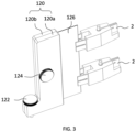
- FIG. 3 is a side view of the cleaning unit in accordance with an embodiment of the present invention.
- FIG. 2 shows the cleaning unit 12 of the cleaning jig 1.
- the cleaning unit 12 has a body 120 on which a first locking member 122, a second locking member 124, and a cleaning sheet 126 are disposed.
- the first locking member 122 can be used to lock the frame 10 of the cleaning jig 1, for example, to lock the first side 100 of the frame 10.
- the frame 10 and the cleaning unit 12 will not move or rotate relatively, so that the cleaning sheet 126 can be kept stable.
- the cleaning unit 12 can be detached from the frame 10, thereby the cleaning unit 12 can be maintained or replaced.
- the body 120 is composed of two similar plate-like structures, which are defined as a first clamping plate 120a and a second clamping plate 120b, and a second locking member 124 can be used to lock the first clamping plate 120a and the second clamping plate 120b.
- the locking directions of the first locking member 122 and the second locking member 124 are different, for example, the locking directions of the first locking member 122 and the second locking member 124 may be perpendicular to each other.
- one end of the cleaning sheet 126 can be sandwiched between the first clamping plate 120a and the second clamping plate 120b, and the other end of the cleaning sheet 126 is exposed to clean the test portion 2.
- the cleaning sheet 126 is a double-sided sheet-like element, and both sides (a first side and a second side) of the cleaning sheet 126 may have sandpaper-like rough surfaces.
- the cleaning sheet 126 may also be a piece of sandpaper folded in half, and the smooth side of the sandpaper is folded inwardly that the rough side of the sandpaper is exposed.
- the first surface and the second surface of the cleaning sheet 126 may both be the same rough side of the sandpaper. It is worth mentioning that this embodiment does not limit how many test portions 2 can clamp one cleaning sheet 126 at the same time.
- FIG. 3 shows that two test portions 2 might clamp one cleaning sheet 126 at the same time, it is also possible that there is only one test portion 2 might clamp the cleaning sheet 126.
- the test portions 2 when the test device tests the electronic component, the test portions 2 not only clamp the electrodes of the electronic component, but also have to rub or friction the electrodes to scrape off the oxide film on the surface of the electrodes. After a period of time, it is inevitable that residues of the oxide film or some dust will adhere to the test portions 2, so the test portions 2 must be cleaned regularly.
- the electronic components on the carrier can be pulled out from a storage location, and put the cleaning jig 1, as the replacement, into the storage location.
- the engineer can issue the same instruction to the test device, for example, the instruction of controlling the test portion 2 of the test device to clamp the electrode of the electronic component.
- this embodiment does not limit the instructions received by the test device, an engineer may also issue instructions designed for the self-cleaning process of the test device.
- the test portion 2 of the test device will clamp the cleaning sheet 126 at the position where the electrode of the electronic component was originally expected to be clamped.
- the test portion 2 has to rub or friction the cleaning sheet 126, the residue and dust accumulated on the test portion 2 can be rubbed off by the rough surface of the cleaning sheet 126, so as to achieve the purpose of cleaning the test portion 2.
- the engineer can give the same instructions more than once to the test device that the test portion 2 can clamp the cleaning sheet 126 several times to improve the cleaning process. It can be seen from the above that the test device can clean itself with the cleaning jig 1, instead of making the cleaning sheet 126 to rub or friction the test portion 2 actively. Therefore, the cleaning process can be completed by giving the existing instructions such as instructions for clamping the electrode.
- the second locking member 124 can also be released to slightly separate the first clamping plate 120a from the second clamping plate 120b.
- the engineer can withdraw the used cleaning sheet 126 from between the first clamping plate 120a and the second clamping plate 120b and replace it with a new one.
- this embodiment has obvious advantages, that is, a cleaning jig 1 can be used to clean a larger number of test portions 2 at one time.
- this embodiment only needs to replace the cleaning sheets 126 to clean the test portions 2 in the next storage location, and the test device does not need to be shut down for cleaning the test portions 2, which also means that the efficiency of the test device can be greatly improved.
- the cleaning jig provided by the present invention can be used to clean the test device, and the test portions of the test device can clamp the cleaning sheet and grind away residues by itself without manually cleaning the test portions one by one.
- the cleaning jig provided by the present invention can quickly clean multiple test portions of the test device in batches, so as to reduce the downtime of the test device due to cleaning, and also reduce the manpower and resources for cleaning the test device.
Landscapes
- Cleaning In General (AREA)
- Testing Electric Properties And Detecting Electric Faults (AREA)
Description
- The present invention pertains to a cleaning jig, more specifically to the cleaning jig for cleaning a test device
- Generally speaking, various electronic equipment might need routine maintenance or cleaning after a period of use to ensure that the electronic equipment can operate normally. In particular, for electronic equipment that requires high precision, such as test devices, it is necessary to perform maintenance or cleaning correctly for reducing errors in measurements. Taking a test device for battery detection as an example, the test device needs to clamp electrodes of a battery with test portions in the first place, and then charge and discharge the battery through the test portions to check whether the battery is working normally. In practice, since the electrodes of the battery are often covered with an oxide film when the battery is manufactured, the test portions also need to scrap off the oxide film while clamping the electrodes. As a result, the surface of each test portion may be stained with scraped oxide film or some residues after a period of use.
- It is understandable that the oxide film on the surface of each test portion may not only affect the efficiency of charging and discharging the battery, but also may interfere with the accuracy of the detection. In addition, because the test portion needs to transmit large current, scraped oxide film or residues on the surface of each test portion may also cause smoke or fire accidents. In practice, it is very important to clean the test portions of the test device regularly, but it is also very troublesome to clean the test portions of the test device. For example, one test device generally needs to test a large number of batteries in batches. Assuming that one electrode of each battery corresponds to one test portion, it can be imagined that the test device will have a large number of test portions. Cleaning the test portions of the test device one by one must be very time-consuming and laborious. The document
KR101527200B - Accordingly, the industry needs a new cleaning jig that can quickly clean multiple test portions of the test device in batches, so as to reduce the downtime of the test device due to cleaning, and also reduce the manpower and resources for cleaning the test device.
- The present invention provides a cleaning jig, which can quickly and massively clean multiple test portions of a test device without stopping the test device, thereby improving the detection efficiency of the test device.
- The present invention discloses a cleaning jig for cleaning a plurality of test portions in a test device. The cleaning jig comprises a frame and a plurality of cleaning units. The frame has a first side which located at an outer edge of the frame. The plurality of cleaning units are detachably disposed on a first side of the frame. Each of the cleaning units has a cleaning sheet, and the cleaning sheet of each of the cleaning units extends outwardly of the frame. Each of the cleaning units corresponds to one of the test portions, and each of the test portions contacts a first surface and a second surface of the corresponding cleaning sheet at the same time.
- In some embodiment, each of the cleaning units may have a first locking member, and the first locking member detachably fixes the first side. Besides, each of the cleaning units may have a second locking member, and the second locking member detachably fixes the cleaning sheet. The locking direction of the first locking member may be different from the locking direction of the second locking member. In addition, the first side and the second side of the cleaning sheet may be made of sandpaper.
- In some embodiment, the test portions of the test device are used to test a plurality of electronic components on a carrier, the frame is defined with a frame length and a frame width, and the frame length may be equal to the length of the carrier, and the frame width may be equal to the width of the carrier. In addition, setting positions of the cleaning units on the first side may correspond to placement positions of the electronic components on the carrier.
- Based on the above, the cleaning jig provided by the present invention can be used to clean the test device, and the test portions of the test device can clamp the cleaning sheet and grind away residues by itself without manually cleaning the test portions one by one. Thereby, the cleaning jig provided by the present invention can quickly clean multiple test portions of the test device in batches, so as to reduce the downtime of the test device due to cleaning, and also reduce the manpower and resources for cleaning the test device.
-
-
FIG. 1 is a perspective view of a cleaning jig in accordance with an embodiment of the present invention. -
FIG. 2 is a perspective view of a cleaning unit in accordance with an embodiment of the present invention. -
FIG. 3 is a side view of the cleaning unit in accordance with an embodiment of the present invention. - The features, objections, and functions of the present invention are further disclosed below. However, it is only a few of the possible embodiments of the present invention, and the scope of the present invention is not limited thereto; that is, the equivalent changes and modifications done in accordance with the claims of the present invention will remain the subject of the present invention. Without departing from the scope of the invention, it should be considered as further enablement of the invention.
- Please refer to
FIG. 1 andFIG. 2 together.FIG. 1 is a perspective view of a cleaning jig in accordance with an embodiment of the present invention.FIG. 2 is a perspective view of a cleaning unit in accordance with an embodiment of the present invention. As shown in figures, thecleaning jig 1 includes aframe 10 and a plurality ofcleaning units 12. The plurality ofcleaning units 12 can be arranged on two sides of theframe 10, and acleaning sheet 126 in each cleaning unit faces or extend toward the outside of theframe 10. In an example, the two sides of theframe 10 can be defined as afirst side 100 and asecond side 102, respectively, and the plurality ofcleaning units 12 can be divided into two groups. One group of thecleaning units 12 is disposed on thefirst side 100, and another group of thecleaning units 12 are disposed on thesecond side 102. As shown inFIG. 1 , the plurality ofcleaning units 12, disposed on thefirst side 100, are arranged in a row, and thecleaning sheets 126 in eachcleaning units 12 are generally oriented at the same angle, for example, vertically toward the outside of theframe 10. - The function of the
cleaning jig 1 is to clean the test device, especially to clean the test portion of the test device (not shown inFIG. 1 ). In practice, when the test device is in normal operation or in use (for example, during testing), the test portion of the test device can be used to test electronic components (not shown). In one example, the electronic component may be a battery, and the test device is a device used to detect whether the battery is working normally. Person having ordinary skill in the art can understand that the test portions need to be firmly electrically connected to the electrodes in the first place, then the charge and discharge tests can be performed. Assuming that the electronic component is a soft-packed battery, since the electrodes of the soft-packed battery are sheet-shaped and flexible, each of the test portion must clamp one electrode to prevent accidentally falling off. Of course, this embodiment does not limit the electronic component to be a soft-pack battery, nor does it limit the electrode to be sheet-shaped. As long as the test portion of the test device is electrically connected to the electrode of the electronic component by clamping the electrode, it should be within the scope of this embodiment. - In order to test electronic components in batches, multiple electronic components can be placed on a carrier (not shown), and then the entire carrier is placed in a storage location of the test device, so that multiple electronic components can be tested together. Correspondingly, the test device will have multiple test portions, so that each test portion can be electrically connected to the electrode of one of the electronic components. This embodiment does not limit the position of the electrode of the electronic component. For example, a plurality of electronic components can be disposed on two sides of the carrier, and the electrode of each electronic component can be perpendicular to the outside of the carrier. In practice, the arrangement of multiple electronic components in the carrier can be similar to the
cleaning jig 1 shown inFIG. 1 of this embodiment. For example, the carrier can be compared to theframe 10 of thecleaning jig 1, and the electronic components can be compared to thecleaning units 12 of thecleaning jig 1, and the electrode of the electronic component can be compared to thecleaning sheet 126 of thecleaning unit 12. At this time, although thecleaning jig 1 does not have real electronic components (such as the battery to be tested), thecleaning jig 1 can still simulate the appearance of the carrier having multiple electronic components. - In order to allow the
cleaning jig 1 to be placed in the storage location of the test device, theframe 10 can be defined with a frame length L and a frame width W, and the frame length L and the frame width W are both smaller than the length and width of the carrier. To simulate the carrier having multiple electronic components even better, the frame length L may also be exactly equal to the length of the carrier, and the frame width W may also be exactly equal to the width of the carrier. In addition, the height of theframe 10 can also be defined as a frame height H, and the frame height H should be smaller than the height of the carrier. In one example, the frame height H can also be exactly equal to the height of the carrier, so that when the frame length L, the frame width W, and the frame height H equal to and the length, width, and height of the carrier, the volume and the appearance of theframe 10 should be roughly the same as the carrier. - In this embodiment, the structure of the cleaning unit will be described, and a way of cleaning the test portion by the cleaning unit will be roughly demonstrated. Please refer to
FIG. 2 andFIG. 3 together.FIG. 2 is a perspective view of a cleaning unit in accordance with an embodiment of the present invention, andFIG. 3 is a side view of the cleaning unit in accordance with an embodiment of the present invention. As shown in the figures,FIG. 2 shows thecleaning unit 12 of the cleaningjig 1. Thecleaning unit 12 has abody 120 on which afirst locking member 122, asecond locking member 124, and acleaning sheet 126 are disposed. Thefirst locking member 122 can be used to lock theframe 10 of the cleaningjig 1, for example, to lock thefirst side 100 of theframe 10. In practice, when thefirst locking member 122 is locked, theframe 10 and thecleaning unit 12 will not move or rotate relatively, so that thecleaning sheet 126 can be kept stable. When thefirst locking member 122 is released, thecleaning unit 12 can be detached from theframe 10, thereby thecleaning unit 12 can be maintained or replaced. - It can be seen from
FIG. 2 that thebody 120 is composed of two similar plate-like structures, which are defined as afirst clamping plate 120a and asecond clamping plate 120b, and asecond locking member 124 can be used to lock thefirst clamping plate 120a and thesecond clamping plate 120b. Moreover, in the example shown inFIG. 2 , the locking directions of thefirst locking member 122 and thesecond locking member 124 are different, for example, the locking directions of thefirst locking member 122 and thesecond locking member 124 may be perpendicular to each other. In one example, one end of thecleaning sheet 126 can be sandwiched between thefirst clamping plate 120a and thesecond clamping plate 120b, and the other end of thecleaning sheet 126 is exposed to clean thetest portion 2. In practice, thecleaning sheet 126 is a double-sided sheet-like element, and both sides (a first side and a second side) of thecleaning sheet 126 may have sandpaper-like rough surfaces. In one example, thecleaning sheet 126 may also be a piece of sandpaper folded in half, and the smooth side of the sandpaper is folded inwardly that the rough side of the sandpaper is exposed. In other words, the first surface and the second surface of thecleaning sheet 126 may both be the same rough side of the sandpaper. It is worth mentioning that this embodiment does not limit howmany test portions 2 can clamp onecleaning sheet 126 at the same time. AlthoughFIG. 3 shows that twotest portions 2 might clamp onecleaning sheet 126 at the same time, it is also possible that there is only onetest portion 2 might clamp thecleaning sheet 126. - Taking a practical example, when the test device tests the electronic component, the
test portions 2 not only clamp the electrodes of the electronic component, but also have to rub or friction the electrodes to scrape off the oxide film on the surface of the electrodes. After a period of time, it is inevitable that residues of the oxide film or some dust will adhere to thetest portions 2, so thetest portions 2 must be cleaned regularly. In one example, after the test device has inspected the electronic components, the electronic components on the carrier can be pulled out from a storage location, and put thecleaning jig 1, as the replacement, into the storage location. Since the position of thecleaning sheet 126 is the same as the electrode position of the electronic component, the engineer can issue the same instruction to the test device, for example, the instruction of controlling thetest portion 2 of the test device to clamp the electrode of the electronic component. Of course, this embodiment does not limit the instructions received by the test device, an engineer may also issue instructions designed for the self-cleaning process of the test device. - Following the above, since the electrode of the electronic component has been replaced with the
cleaning sheet 126, thetest portion 2 of the test device will clamp thecleaning sheet 126 at the position where the electrode of the electronic component was originally expected to be clamped. Person having ordinary skill in the art can understand that because thetest portion 2 has to rub or friction thecleaning sheet 126, the residue and dust accumulated on thetest portion 2 can be rubbed off by the rough surface of thecleaning sheet 126, so as to achieve the purpose of cleaning thetest portion 2. In one example, if thetest portion 2 accumulates a lot of dirt, in order to clean thetest portion 2 completely, the engineer can give the same instructions more than once to the test device that thetest portion 2 can clamp thecleaning sheet 126 several times to improve the cleaning process. It can be seen from the above that the test device can clean itself with the cleaningjig 1, instead of making thecleaning sheet 126 to rub or friction thetest portion 2 actively. Therefore, the cleaning process can be completed by giving the existing instructions such as instructions for clamping the electrode. - In addition, when the
cleaning sheet 126 reaches the suggested replacement usage (for example, after a lot of uses), thesecond locking member 124 can also be released to slightly separate thefirst clamping plate 120a from thesecond clamping plate 120b. At this time, the engineer can withdraw the usedcleaning sheet 126 from between thefirst clamping plate 120a and thesecond clamping plate 120b and replace it with a new one. Compared with shutting down the test device and disassembling and cleaning thetest portions 2 one by one, this embodiment has obvious advantages, that is, a cleaningjig 1 can be used to clean a larger number oftest portions 2 at one time. On the other hand, this embodiment only needs to replace thecleaning sheets 126 to clean thetest portions 2 in the next storage location, and the test device does not need to be shut down for cleaning thetest portions 2, which also means that the efficiency of the test device can be greatly improved. - In summary, the cleaning jig provided by the present invention can be used to clean the test device, and the test portions of the test device can clamp the cleaning sheet and grind away residues by itself without manually cleaning the test portions one by one. Thereby, the cleaning jig provided by the present invention can quickly clean multiple test portions of the test device in batches, so as to reduce the downtime of the test device due to cleaning, and also reduce the manpower and resources for cleaning the test device.
Claims (5)
- A cleaning jig (1) for simultaneous cleaning of a plurality of test portions in a test device, the cleaning jig comprising:a frame (10) having a first side located at an outer edge of the frame; anda plurality of cleaning units (12) detachably disposed on a first side of the frame;wherein each of the cleaning units has a cleaning sheet (126), and the cleaning sheet of each of the cleaning units extends outwardly of the frame;wherein the position of each of the cleaning units corresponds to the position of one of the test portions (2), and wherein the cleaning units and the test portions are adapted in such a way that each of the test portions, when in use, contacts a first surface and a second surface of the corresponding cleaning sheet at the same time.
- The cleaning jig according to claim 1, wherein each of the cleaning units has a first locking member (122), and the first locking member detachably fixes the first side.
- The cleaning jig according to claim 2, wherein each of the cleaning units has a second locking member (124), and the second locking member detachably fixes the cleaning sheet.
- The cleaning jig according to claim 3, wherein the locking direction of the first locking member is different from the locking direction of the second locking member.
- The cleaning jig according to any of claims 1-4, wherein the first side and the second side of the cleaning sheet are made of sandpaper.
Applications Claiming Priority (1)
| Application Number | Priority Date | Filing Date | Title |
|---|---|---|---|
| TW109119762A TWI749588B (en) | 2020-06-12 | 2020-06-12 | Cleaning system |
Publications (3)
| Publication Number | Publication Date |
|---|---|
| EP3922366A1 EP3922366A1 (en) | 2021-12-15 |
| EP3922366C0 EP3922366C0 (en) | 2023-07-26 |
| EP3922366B1 true EP3922366B1 (en) | 2023-07-26 |
Family
ID=76392199
Family Applications (1)
| Application Number | Title | Priority Date | Filing Date |
|---|---|---|---|
| EP21178866.6A Active EP3922366B1 (en) | 2020-06-12 | 2021-06-10 | Cleaning jig |
Country Status (3)
| Country | Link |
|---|---|
| EP (1) | EP3922366B1 (en) |
| JP (1) | JP7274525B2 (en) |
| TW (1) | TWI749588B (en) |
Family Cites Families (8)
| Publication number | Priority date | Publication date | Assignee | Title |
|---|---|---|---|---|
| JP2004031358A (en) * | 2003-07-25 | 2004-01-29 | Renesas Technology Corp | Manufacturing method of semiconductor device and foreign matter removing sheet |
| WO2008120519A1 (en) * | 2007-03-29 | 2008-10-09 | Advantest Corporation | Tcp handling apparatus |
| KR101527200B1 (en) * | 2012-08-28 | 2015-06-09 | (주)에이티테크놀러지 | Apparatus for cleaning test jig for testing electrical condition of electronic component and apparatus for testing electronic component having the same |
| JP6244738B2 (en) * | 2013-08-19 | 2017-12-13 | 株式会社富士通テレコムネットワークス福島 | Automatic cleaning unit and charge / discharge test system |
| TWI599779B (en) * | 2016-07-11 | 2017-09-21 | 致茂電子股份有限公司 | Clipped probing device |
| TWM546863U (en) * | 2017-04-21 | 2017-08-11 | ye-qing Zhang | Cement hole brush and cleaning component thereof |
| TWI668460B (en) * | 2018-06-12 | 2019-08-11 | 致茂電子股份有限公司 | Clipped testing device |
| CN210098330U (en) * | 2019-05-20 | 2020-02-21 | 河南久之盛智能科技有限公司 | Electronic component surface cleaning device |
-
2020
- 2020-06-12 TW TW109119762A patent/TWI749588B/en active
-
2021
- 2021-06-10 EP EP21178866.6A patent/EP3922366B1/en active Active
- 2021-06-11 JP JP2021097716A patent/JP7274525B2/en active Active
Also Published As
| Publication number | Publication date |
|---|---|
| TW202146124A (en) | 2021-12-16 |
| EP3922366C0 (en) | 2023-07-26 |
| JP2022003330A (en) | 2022-01-11 |
| TWI749588B (en) | 2021-12-11 |
| JP7274525B2 (en) | 2023-05-16 |
| EP3922366A1 (en) | 2021-12-15 |
Similar Documents
| Publication | Publication Date | Title |
|---|---|---|
| KR102291536B1 (en) | Apparatus and method for testing a battery pack | |
| KR102287763B1 (en) | Manufacturing system of battery cell | |
| EP3026439A2 (en) | Contact inspection device | |
| EP3922366A1 (en) | Cleaning jig | |
| KR101650504B1 (en) | Device for inspecting quality of battery pack | |
| CN110763548A (en) | Bending test fixture for flexible display screen | |
| CN113798220B (en) | Cleaning jig | |
| CN103868937A (en) | Touch screen detection fixture | |
| CN211554256U (en) | Jig for testing probe | |
| JP6244738B2 (en) | Automatic cleaning unit and charge / discharge test system | |
| JP6049001B2 (en) | Weighing device | |
| CN104345182A (en) | Multi-station test clamp | |
| CN203566037U (en) | Welding tool | |
| CN106653633A (en) | Battery piece for detecting abnormality of probe row and operation method used for detection | |
| CN205262998U (en) | Electronic component testing machine and testing device | |
| CN211234932U (en) | False welding tool for inspecting series welding machine | |
| CN221676939U (en) | A battery pack detection fixture | |
| KR101699124B1 (en) | Integrated jig | |
| CN221446214U (en) | Detection device | |
| CN217331020U (en) | Flatness detection device | |
| CN218236735U (en) | High efficiency X ray nondestructive inspection mechanism | |
| JP7596618B2 (en) | Tab guide and tab guide device including the tab guide | |
| CN218427269U (en) | Cutter detection device | |
| CN224176599U (en) | A portable intelligent inspection system for faults in old refining plates | |
| TWI567382B (en) | Optical detection machine |
Legal Events
| Date | Code | Title | Description |
|---|---|---|---|
| PUAI | Public reference made under article 153(3) epc to a published international application that has entered the european phase |
Free format text: ORIGINAL CODE: 0009012 |
|
| STAA | Information on the status of an ep patent application or granted ep patent |
Free format text: STATUS: REQUEST FOR EXAMINATION WAS MADE |
|
| 17P | Request for examination filed |
Effective date: 20210710 |
|
| AK | Designated contracting states |
Kind code of ref document: A1 Designated state(s): AL AT BE BG CH CY CZ DE DK EE ES FI FR GB GR HR HU IE IS IT LI LT LU LV MC MK MT NL NO PL PT RO RS SE SI SK SM TR |
|
| B565 | Issuance of search results under rule 164(2) epc |
Effective date: 20211021 |
|
| RBV | Designated contracting states (corrected) |
Designated state(s): AL AT BE BG CH CY CZ DE DK EE ES FI FR GB GR HR HU IE IS IT LI LT LU LV MC MK MT NL NO PL PT RO RS SE SI SK SM TR |
|
| RIN1 | Information on inventor provided before grant (corrected) |
Inventor name: CHANG, WEN-CHUAN Inventor name: CHUANG, MING-JU Inventor name: WANG, YU-KUANG Inventor name: LEE, JIH-HSING |
|
| GRAP | Despatch of communication of intention to grant a patent |
Free format text: ORIGINAL CODE: EPIDOSNIGR1 |
|
| STAA | Information on the status of an ep patent application or granted ep patent |
Free format text: STATUS: GRANT OF PATENT IS INTENDED |
|
| INTG | Intention to grant announced |
Effective date: 20230206 |
|
| GRAS | Grant fee paid |
Free format text: ORIGINAL CODE: EPIDOSNIGR3 |
|
| GRAA | (expected) grant |
Free format text: ORIGINAL CODE: 0009210 |
|
| STAA | Information on the status of an ep patent application or granted ep patent |
Free format text: STATUS: THE PATENT HAS BEEN GRANTED |
|
| AK | Designated contracting states |
Kind code of ref document: B1 Designated state(s): AL AT BE BG CH CY CZ DE DK EE ES FI FR GB GR HR HU IE IS IT LI LT LU LV MC MK MT NL NO PL PT RO RS SE SI SK SM TR |
|
| REG | Reference to a national code |
Ref country code: CH Ref legal event code: EP |
|
| REG | Reference to a national code |
Ref country code: DE Ref legal event code: R096 Ref document number: 602021003734 Country of ref document: DE |
|
| REG | Reference to a national code |
Ref country code: IE Ref legal event code: FG4D |
|
| U01 | Request for unitary effect filed |
Effective date: 20230822 |
|
| U07 | Unitary effect registered |
Designated state(s): AT BE BG DE DK EE FI FR IT LT LU LV MT NL PT SE SI Effective date: 20230828 |
|
| REG | Reference to a national code |
Ref country code: LT Ref legal event code: MG9D |
|
| PG25 | Lapsed in a contracting state [announced via postgrant information from national office to epo] |
Ref country code: GR Free format text: LAPSE BECAUSE OF FAILURE TO SUBMIT A TRANSLATION OF THE DESCRIPTION OR TO PAY THE FEE WITHIN THE PRESCRIBED TIME-LIMIT Effective date: 20231027 |
|
| PG25 | Lapsed in a contracting state [announced via postgrant information from national office to epo] |
Ref country code: IS Free format text: LAPSE BECAUSE OF FAILURE TO SUBMIT A TRANSLATION OF THE DESCRIPTION OR TO PAY THE FEE WITHIN THE PRESCRIBED TIME-LIMIT Effective date: 20231126 |
|
| PG25 | Lapsed in a contracting state [announced via postgrant information from national office to epo] |
Ref country code: RS Free format text: LAPSE BECAUSE OF FAILURE TO SUBMIT A TRANSLATION OF THE DESCRIPTION OR TO PAY THE FEE WITHIN THE PRESCRIBED TIME-LIMIT Effective date: 20230726 Ref country code: NO Free format text: LAPSE BECAUSE OF FAILURE TO SUBMIT A TRANSLATION OF THE DESCRIPTION OR TO PAY THE FEE WITHIN THE PRESCRIBED TIME-LIMIT Effective date: 20231026 Ref country code: IS Free format text: LAPSE BECAUSE OF FAILURE TO SUBMIT A TRANSLATION OF THE DESCRIPTION OR TO PAY THE FEE WITHIN THE PRESCRIBED TIME-LIMIT Effective date: 20231126 Ref country code: HR Free format text: LAPSE BECAUSE OF FAILURE TO SUBMIT A TRANSLATION OF THE DESCRIPTION OR TO PAY THE FEE WITHIN THE PRESCRIBED TIME-LIMIT Effective date: 20230726 Ref country code: GR Free format text: LAPSE BECAUSE OF FAILURE TO SUBMIT A TRANSLATION OF THE DESCRIPTION OR TO PAY THE FEE WITHIN THE PRESCRIBED TIME-LIMIT Effective date: 20231027 |
|
| PG25 | Lapsed in a contracting state [announced via postgrant information from national office to epo] |
Ref country code: PL Free format text: LAPSE BECAUSE OF FAILURE TO SUBMIT A TRANSLATION OF THE DESCRIPTION OR TO PAY THE FEE WITHIN THE PRESCRIBED TIME-LIMIT Effective date: 20230726 |
|
| PG25 | Lapsed in a contracting state [announced via postgrant information from national office to epo] |
Ref country code: ES Free format text: LAPSE BECAUSE OF FAILURE TO SUBMIT A TRANSLATION OF THE DESCRIPTION OR TO PAY THE FEE WITHIN THE PRESCRIBED TIME-LIMIT Effective date: 20230726 |
|
| REG | Reference to a national code |
Ref country code: DE Ref legal event code: R097 Ref document number: 602021003734 Country of ref document: DE |
|
| PG25 | Lapsed in a contracting state [announced via postgrant information from national office to epo] |
Ref country code: SM Free format text: LAPSE BECAUSE OF FAILURE TO SUBMIT A TRANSLATION OF THE DESCRIPTION OR TO PAY THE FEE WITHIN THE PRESCRIBED TIME-LIMIT Effective date: 20230726 Ref country code: RO Free format text: LAPSE BECAUSE OF FAILURE TO SUBMIT A TRANSLATION OF THE DESCRIPTION OR TO PAY THE FEE WITHIN THE PRESCRIBED TIME-LIMIT Effective date: 20230726 Ref country code: ES Free format text: LAPSE BECAUSE OF FAILURE TO SUBMIT A TRANSLATION OF THE DESCRIPTION OR TO PAY THE FEE WITHIN THE PRESCRIBED TIME-LIMIT Effective date: 20230726 Ref country code: CZ Free format text: LAPSE BECAUSE OF FAILURE TO SUBMIT A TRANSLATION OF THE DESCRIPTION OR TO PAY THE FEE WITHIN THE PRESCRIBED TIME-LIMIT Effective date: 20230726 Ref country code: SK Free format text: LAPSE BECAUSE OF FAILURE TO SUBMIT A TRANSLATION OF THE DESCRIPTION OR TO PAY THE FEE WITHIN THE PRESCRIBED TIME-LIMIT Effective date: 20230726 |
|
| PLBE | No opposition filed within time limit |
Free format text: ORIGINAL CODE: 0009261 |
|
| STAA | Information on the status of an ep patent application or granted ep patent |
Free format text: STATUS: NO OPPOSITION FILED WITHIN TIME LIMIT |
|
| 26N | No opposition filed |
Effective date: 20240429 |
|
| U20 | Renewal fee for the european patent with unitary effect paid |
Year of fee payment: 4 Effective date: 20240620 |
|
| PG25 | Lapsed in a contracting state [announced via postgrant information from national office to epo] |
Ref country code: MC Free format text: LAPSE BECAUSE OF FAILURE TO SUBMIT A TRANSLATION OF THE DESCRIPTION OR TO PAY THE FEE WITHIN THE PRESCRIBED TIME-LIMIT Effective date: 20230726 |
|
| REG | Reference to a national code |
Ref country code: CH Ref legal event code: PL |
|
| PG25 | Lapsed in a contracting state [announced via postgrant information from national office to epo] |
Ref country code: IE Free format text: LAPSE BECAUSE OF NON-PAYMENT OF DUE FEES Effective date: 20240610 |
|
| PG25 | Lapsed in a contracting state [announced via postgrant information from national office to epo] |
Ref country code: CH Free format text: LAPSE BECAUSE OF NON-PAYMENT OF DUE FEES Effective date: 20240630 |
|
| U20 | Renewal fee for the european patent with unitary effect paid |
Year of fee payment: 5 Effective date: 20250527 |
|
| PGFP | Annual fee paid to national office [announced via postgrant information from national office to epo] |
Ref country code: GB Payment date: 20250528 Year of fee payment: 5 |
|
| PG25 | Lapsed in a contracting state [announced via postgrant information from national office to epo] |
Ref country code: CY Free format text: LAPSE BECAUSE OF FAILURE TO SUBMIT A TRANSLATION OF THE DESCRIPTION OR TO PAY THE FEE WITHIN THE PRESCRIBED TIME-LIMIT; INVALID AB INITIO Effective date: 20210610 |
|
| PG25 | Lapsed in a contracting state [announced via postgrant information from national office to epo] |
Ref country code: HU Free format text: LAPSE BECAUSE OF FAILURE TO SUBMIT A TRANSLATION OF THE DESCRIPTION OR TO PAY THE FEE WITHIN THE PRESCRIBED TIME-LIMIT; INVALID AB INITIO Effective date: 20210610 |