EP3909236B1 - Systeme, vorrichtung und verfahren zur inspektion von fluoreszenzmikroskopie - Google Patents
Systeme, vorrichtung und verfahren zur inspektion von fluoreszenzmikroskopie Download PDFInfo
- Publication number
- EP3909236B1 EP3909236B1 EP20753126.0A EP20753126A EP3909236B1 EP 3909236 B1 EP3909236 B1 EP 3909236B1 EP 20753126 A EP20753126 A EP 20753126A EP 3909236 B1 EP3909236 B1 EP 3909236B1
- Authority
- EP
- European Patent Office
- Prior art keywords
- specimen
- light
- image data
- darkfield
- filter
- Prior art date
- Legal status (The legal status is an assumption and is not a legal conclusion. Google has not performed a legal analysis and makes no representation as to the accuracy of the status listed.)
- Active
Links
Images


Classifications
-
- G—PHYSICS
- G02—OPTICS
- G02B—OPTICAL ELEMENTS, SYSTEMS OR APPARATUS
- G02B21/00—Microscopes
- G02B21/0004—Microscopes specially adapted for specific applications
- G02B21/002—Scanning microscopes
- G02B21/0024—Confocal scanning microscopes (CSOMs) or confocal "macroscopes"; Accessories which are not restricted to use with CSOMs, e.g. sample holders
- G02B21/0052—Optical details of the image generation
- G02B21/0076—Optical details of the image generation arrangements using fluorescence or luminescence
-
- G—PHYSICS
- G01—MEASURING; TESTING
- G01N—INVESTIGATING OR ANALYSING MATERIALS BY DETERMINING THEIR CHEMICAL OR PHYSICAL PROPERTIES
- G01N21/00—Investigating or analysing materials by the use of optical means, i.e. using sub-millimetre waves, infrared, visible or ultraviolet light
- G01N21/62—Systems in which the material investigated is excited whereby it emits light or causes a change in wavelength of the incident light
- G01N21/63—Systems in which the material investigated is excited whereby it emits light or causes a change in wavelength of the incident light optically excited
- G01N21/64—Fluorescence; Phosphorescence
- G01N21/645—Specially adapted constructive features of fluorimeters
- G01N21/6456—Spatial resolved fluorescence measurements; Imaging
- G01N21/6458—Fluorescence microscopy
-
- G—PHYSICS
- G01—MEASURING; TESTING
- G01N—INVESTIGATING OR ANALYSING MATERIALS BY DETERMINING THEIR CHEMICAL OR PHYSICAL PROPERTIES
- G01N21/00—Investigating or analysing materials by the use of optical means, i.e. using sub-millimetre waves, infrared, visible or ultraviolet light
- G01N21/84—Systems specially adapted for particular applications
- G01N21/88—Investigating the presence of flaws or contamination
- G01N21/8806—Specially adapted optical and illumination features
-
- G—PHYSICS
- G02—OPTICS
- G02B—OPTICAL ELEMENTS, SYSTEMS OR APPARATUS
- G02B21/00—Microscopes
- G02B21/0004—Microscopes specially adapted for specific applications
- G02B21/0016—Technical microscopes, e.g. for inspection or measuring in industrial production processes
-
- G—PHYSICS
- G02—OPTICS
- G02B—OPTICAL ELEMENTS, SYSTEMS OR APPARATUS
- G02B21/00—Microscopes
- G02B21/06—Means for illuminating specimens
- G02B21/08—Condensers
- G02B21/12—Condensers affording bright-field illumination
- G02B21/125—Condensers affording bright-field illumination affording both dark- and bright-field illumination
-
- G—PHYSICS
- G02—OPTICS
- G02B—OPTICAL ELEMENTS, SYSTEMS OR APPARATUS
- G02B21/00—Microscopes
- G02B21/16—Microscopes adapted for ultraviolet illumination ; Fluorescence microscopes
-
- G—PHYSICS
- G02—OPTICS
- G02B—OPTICAL ELEMENTS, SYSTEMS OR APPARATUS
- G02B21/00—Microscopes
- G02B21/18—Arrangements with more than one light path, e.g. for comparing two specimens
-
- G—PHYSICS
- G02—OPTICS
- G02B—OPTICAL ELEMENTS, SYSTEMS OR APPARATUS
- G02B21/00—Microscopes
- G02B21/36—Microscopes arranged for photographic purposes or projection purposes or digital imaging or video purposes including associated control and data processing arrangements
- G02B21/361—Optical details, e.g. image relay to the camera or image sensor
-
- G—PHYSICS
- G02—OPTICS
- G02B—OPTICAL ELEMENTS, SYSTEMS OR APPARATUS
- G02B21/00—Microscopes
- G02B21/36—Microscopes arranged for photographic purposes or projection purposes or digital imaging or video purposes including associated control and data processing arrangements
- G02B21/365—Control or image processing arrangements for digital or video microscopes
- G02B21/367—Control or image processing arrangements for digital or video microscopes providing an output produced by processing a plurality of individual source images, e.g. image tiling, montage, composite images, depth sectioning, image comparison
-
- G—PHYSICS
- G06—COMPUTING OR CALCULATING; COUNTING
- G06T—IMAGE DATA PROCESSING OR GENERATION, IN GENERAL
- G06T7/00—Image analysis
- G06T7/0002—Inspection of images, e.g. flaw detection
- G06T7/0004—Industrial image inspection
-
- G—PHYSICS
- G06—COMPUTING OR CALCULATING; COUNTING
- G06V—IMAGE OR VIDEO RECOGNITION OR UNDERSTANDING
- G06V20/00—Scenes; Scene-specific elements
- G06V20/60—Type of objects
- G06V20/69—Microscopic objects, e.g. biological cells or cellular parts
- G06V20/693—Acquisition
-
- G—PHYSICS
- G06—COMPUTING OR CALCULATING; COUNTING
- G06V—IMAGE OR VIDEO RECOGNITION OR UNDERSTANDING
- G06V20/00—Scenes; Scene-specific elements
- G06V20/60—Type of objects
- G06V20/69—Microscopic objects, e.g. biological cells or cellular parts
- G06V20/698—Matching; Classification
-
- H—ELECTRICITY
- H04—ELECTRIC COMMUNICATION TECHNIQUE
- H04N—PICTORIAL COMMUNICATION, e.g. TELEVISION
- H04N23/00—Cameras or camera modules comprising electronic image sensors; Control thereof
- H04N23/90—Arrangement of cameras or camera modules, e.g. multiple cameras in TV studios or sports stadiums
-
- G—PHYSICS
- G01—MEASURING; TESTING
- G01N—INVESTIGATING OR ANALYSING MATERIALS BY DETERMINING THEIR CHEMICAL OR PHYSICAL PROPERTIES
- G01N21/00—Investigating or analysing materials by the use of optical means, i.e. using sub-millimetre waves, infrared, visible or ultraviolet light
- G01N21/84—Systems specially adapted for particular applications
- G01N21/88—Investigating the presence of flaws or contamination
- G01N21/8851—Scan or image signal processing specially adapted therefor, e.g. for scan signal adjustment, for detecting different kinds of defects, for compensating for structures, markings, edges
- G01N2021/8883—Scan or image signal processing specially adapted therefor, e.g. for scan signal adjustment, for detecting different kinds of defects, for compensating for structures, markings, edges involving the calculation of gauges, generating models
-
- G—PHYSICS
- G06—COMPUTING OR CALCULATING; COUNTING
- G06T—IMAGE DATA PROCESSING OR GENERATION, IN GENERAL
- G06T2207/00—Indexing scheme for image analysis or image enhancement
- G06T2207/10—Image acquisition modality
- G06T2207/10056—Microscopic image
-
- G—PHYSICS
- G06—COMPUTING OR CALCULATING; COUNTING
- G06T—IMAGE DATA PROCESSING OR GENERATION, IN GENERAL
- G06T2207/00—Indexing scheme for image analysis or image enhancement
- G06T2207/10—Image acquisition modality
- G06T2207/10064—Fluorescence image
-
- G—PHYSICS
- G06—COMPUTING OR CALCULATING; COUNTING
- G06T—IMAGE DATA PROCESSING OR GENERATION, IN GENERAL
- G06T2207/00—Indexing scheme for image analysis or image enhancement
- G06T2207/10—Image acquisition modality
- G06T2207/10141—Special mode during image acquisition
- G06T2207/10152—Varying illumination
-
- G—PHYSICS
- G06—COMPUTING OR CALCULATING; COUNTING
- G06T—IMAGE DATA PROCESSING OR GENERATION, IN GENERAL
- G06T2207/00—Indexing scheme for image analysis or image enhancement
- G06T2207/20—Special algorithmic details
- G06T2207/20084—Artificial neural networks [ANN]
-
- G—PHYSICS
- G06—COMPUTING OR CALCULATING; COUNTING
- G06T—IMAGE DATA PROCESSING OR GENERATION, IN GENERAL
- G06T2207/00—Indexing scheme for image analysis or image enhancement
- G06T2207/30—Subject of image; Context of image processing
- G06T2207/30108—Industrial image inspection
- G06T2207/30148—Semiconductor; IC; Wafer
Definitions
- the present disclosure generally relates to fluorescence microscopy inspection systems, apparatus and methods using incoherent illumination techniques. More particularly, embodiments of the present invention relate to fluorescence microscopy inspection systems that can provide incoherent light of variable wavelengths targeted to excite specific layers of a specimen or materials contained in a specimen and automatically detect features of a specimen from the resulting fluorescence caused by the absorption of light or other electromagnetic radiation.
- US 2018/188188 discloses an inspection system that includes an illumination source to generate an illumination beam, focusing elements to direct the illumination beam to a sample, a detector, collection elements configured to direct radiation emanating from the sample to the detector, a detection mode control device to image the sample in two or more detection modes such that the detector generates two or more collection signals based on the two or more detection modes, and a controller.
- Radiation emanating from the sample includes at least radiation specularly reflected by the sample and radiation scattered by the sample.
- the controller determines defect scattering characteristics associated with radiation scattered by defects on the sample based on the two or more collection signals.
- the controller also classifies the one or more particles according to a set of predetermined defect classifications based on the one or more defect scattering characteristics.
- US 2007/121106 discloses a variety of optical functions applicable to various kinds of objects to be inspected. For each, it describes accumulating contrasts (brightness differences), etc. of defects to be detected (DOI) and false defects not to be detected ( nuisance), and the selection of parameters for inspection with high sensitivity and low nuisance ratio.
- DOI defects to be detected
- nuisance false defects not to be detected
- a wavelength band, an illumination scheme, and filtering parameters can be selected for an optical system.
- WO 2018/229709 discloses a method for automatic defect classification including (i) acquiring, by a first camera, at least one first image of at least one area of an object; (ii) processing the at least one first image to detect a group of suspected defects within the at least one area; (iii) performing a first classification process for initially classifying the group of suspected defects; (iii) determining whether a first subgroup of the suspected defects requires additional information from a second camera for a completion of a classification; (iv) when determining that the first subgroup of the suspected defects requires additional information from the second camera then: (a) acquiring second images, by the second camera, of the first subgroup of the suspected defects; and (b) performing a second classification process for classifying the first subgroup of suspected defects.
- Projecting non-visible light at a specimen and capturing the resulting fluorescence/ photoluminescence emitted by a specimen can provide important information about the quantity, type, location and morphology of features on a specimen. Further, certain features of a specimen, such as the purity or structural imperfections of the specimen, among others, may only be observed using non-visible illumination.
- Specimens as understood by a person of ordinary skill in the art refer to an article of examination (e.g., a wafer or a biological slide) and features refer to observable characteristics of a specimen, including abnormalities and/or defects.
- Features can include but are not limited to: circuits, circuit board components, biological cells, tissue, defects (e.g., impurities, structural imperfections, irregularities, stacking faults, contaminants, crystallographic defects, scratches, dust, fingerprints).
- fluorescence includes photoluminescense, which is commonly associated with light emissions from semiconductor materials.
- Non-visible light refers to the region of the electroagnetic spectrum with a wavelength between 10 and 400 nanometers (nm) (i.e., the region between visible light and X-rays). In some embodiments, for example, light wavelengths in the range of 200nm to 400nm, 300nm to 400nm, and/or any other suitable wavelengths can be selected.
- the light wavelength required to excite a specimen and cause fluoresencese by a specimen from the absorption of light or other electromagnetic radiation is not restricted to the wavelength range between 10nm to 400nm, but, in some embodiments, can be selected in a range above 400nm to provide the desired excitation to a specimen, as explained herein.
- Coherent light refers to particles of light energy that have the same frequency and its waves are in phase with one another. In contrast, the particles of light energy of incoherent light do not have the same frequency and its waves are not in phase with one another.
- coherent light sources e.g., lasers
- incoherent light sources are commonly used for specimen fluorescence
- coherent light sources are not ideal for detecting large features or for use with certain types of specimens (e.g., patterned wafers).
- Incoherent light sources are better suited for detecting a greater range of features (including large features and features on patterned wafers).
- coherent light sources illuminate only a small portion of a field of view
- incoherent light illuminates the entire field of view, making it more suitable for creating specimen feature maps.
- Specimen feature maps classify features on a specimen and specify their location.
- field of view as understood by a person of ordinary skill in the art refers to an area of examination that is captured at once by an image sensor. Further, a person of ordinary skill in the art will readily understand that the terms field of view and image are used interchangeably herein.
- new fluorescence microscopy inspection mechanisms using incoherent illumination techniques are desirable to excite specific layers of a specimen or materials contained in a specimen to cause them to fluoresce and to automatically detect features of a specimen from the resulting fluorescence. Moreover, it is also desirable for the same mechanisms to inspect features of a specimen using illumination techniques that do not cause fluorescence.
- microscopy system as defined in claim 1.
- a darkfield insert is fastened to the attachment and positioned above the darkfield channel of the objective, the darkfield insert including a ring of lights configured to project light at the specimen at an oblique angle.
- mechanisms (which can include systems, methods, devices, apparatuses, etc.) for fluorescence microscopy inspection using incoherent illumination techniques to excite specific layers of a specimen or materials contained in a specimen to cause them to fluoresce and to automatically detect features of a specimen from the resulting fluorescence are provided.
- the same mechanism can be also be used to inspect features of a specimen using illumination techniques that do not cause fluorescence.
- a pigment can be added to a specimen and incoherent illumination techniques can be used targeted to the pigment to cause it to fluoresce. Inspection (sometimes referred to as examination) refers to scanning, imaging, analyzing, measuring and any other suitable review of a specimen using the disclosed incoherent microscopy inspection mechanism for fluorescence imaging.
- FIGS. 1A and 1B illustrate examples of fluorescence microscopy inspection systems using incoherent illumination for automatically analyzing fluorescence emitted from a specimen (referred to herein as "FMIS 100"), according to some embodiments of the disclosed subject matter.
- the basic components of FMIS 100 include one or more illumination sources (e.g. light sources 25, 25a and 28) for providing incoherent light, a focusing mechanism 32 for finding the in-focus plane of a specimen, an illuminator 22, an imaging device 6, one or more objectives 35, a stage 30, one or more filter mechanisms 15, a brightfield/darkfield slider 40 and a control module 110 comprising hardware, software, and/or firmware and a computer analysis system 115.
- illumination sources e.g. light sources 25, 25a and 28
- a focusing mechanism 32 for finding the in-focus plane of a specimen
- an illuminator 22 for finding the in-focus plane of a specimen
- an illuminator 22 for finding the in-focus plane of a specimen
- control module 110, and computer analysis system 115 are coupled to inspection system 100 via a communication channel 120.
- communication channel 120 can include one or more signal transmitting means, such as a bus, or wireless RF channel.
- FMIS 100 can include additional microscope components that are well known in the art.
- FMIS 100 may include a frame (not depicted) to which the various components of FMIS 100 (e.g., one or more illumination sources, a focusing mechanism, an illuminator, an imaging device, one or more objectives, a stage, one or fore filter mechanisms, a brightfield/darkfield slider, a control module, a nosepiece, a beam splitter) may be connected (e.g., for portability, stability, modular support, etc.).
- a computer analysis system may be connected to the frame and in some embodiments it may not.
- Other microscope components not listed herein, but well known in the art, can also be connected to the frame.
- FMIS 100 can be implemented as part of any suitable type of microscope.
- FMIS 100 can be implemented as part of an optical microscope that uses reflected light (as shown in FIG. 1A ) and/or transmitted light (as shown in FIG. 1B ). More particularly, FMIS 100 can be implemented as part of the nSpec ® optical microscope available from Nanotronics Imaging, Inc. of Cuyahoga Falls, OH.
- an XY translation stage can be used for stage 30.
- the XY translation stage can be driven by stepper motor, servo motor, linear motor, piezo motor, and/or any other suitable mechanism.
- the XY translation stage can be configured to move a specimen in the X axis and/or Y axis directions under the control of any suitable controller, in some embodiments.
- a focus mechanism 32 coupled to stage 30 can be used to adjust the stage in a Z direction towards and away from objective 35.
- Focus mechanism 32 can be used to make coarse focus adjustments of, for example, 0 to 5 mm, 0 to 10 mm, 0 to 30 mm, and/or any other suitable range(s) of distances.
- Focus mechanism 32 can also be used to move stage 30 up and down to allow specimens of different thicknesses to be placed on the stage.
- Focus mechanism 32 can also be used in some embodiments to provide fine focus of, for example, 0 to 50 ⁇ m, 0 to 100 ⁇ m, 0 to 200 ⁇ m, and/or any other suitable range(s) of distances.
- focus mechanism 32 can also include a location device.
- the location device can be configured to determine a position of stage 30 at any suitable point in time.
- any suitable position e.g., the position of the stage when a specimen is in focus
- the location device can be a linear encoder, a rotary encoder or any other suitable mechanism to track the absolute position of stage 30 with respect to the objective.
- FMIS 100 can include, one or more objectives 35.
- the objectives can have different magnification powers and/or be configured to operate with fluorescence, as well as brightfield/darkfield, differential interference contrast (DIC), polarized light, cross-polarized light, and/or any other suitable form of illumination.
- DIC differential interference contrast
- the objective and/or illumination technique used to inspect a specimen can be controlled by software, hardware, and/or firmware in some embodiments.
- a second focus mechanism (not shown) can be used to drive objective 35 in a Z direction towards and away from stage 30.
- the second focus mechanism can be designed for coarse or fine focus adjustment of objective 35.
- the second focus mechanism can be a stepper motor, servo motor, linear actuator, piezo motor, and/or any other suitable mechanism.
- a piezo motor can be used and can drive the objective 0 to 50 micrometers ( ⁇ m), 0 to 100 ⁇ m, or 0 to 200 ⁇ m, and/or any other suitable range(s) of distances.
- communication between the control module (e.g., the controller and controller interface) and the components of FMIS 100 can use any suitable communication technologies, that provide the ability to communicate with one or more other devices, and/or to transact data with a computer network.
- implemented communication technologies can include, but are not limited to: analog technologies (e.g., relay logic), digital technologies (e.g., RS232, ethernet, or wireless), network technologies (e.g., local area network (LAN), a wide area network (WAN), the Internet, Bluetooth technologies, Near-field communication technologies, Secure RF technologies, and/or any other suitable communication technologies.
- operator inputs can be communicated to control module 110 using any suitable input device (e.g., keyboard, mouse, joystick, touch, touch-screen, etc.).
- suitable input device e.g., keyboard, mouse, joystick, touch, touch-screen, etc.
- computer analysis system 115 can be coupled to, or included in, FMIS 100 in any suitable manner using any suitable communication technology, such as analog technologies (e.g., relay logic), digital technologies (e.g., RS232, ethernet, or wireless), network technologies (e.g., local area network (LAN), a wide area network (WAN), the Internet) Bluetooth technologies, Near-field communication technologies, Secure RF technologies, and/or any other suitable communication technologies.
- Computer analysis system 115, and the modules within computer analysis system 115 can be configured to perform a number of functions described further herein using images output by FMIS 100 and/or stored by computer readable media.
- Computer analysis system 115 can include any suitable hardware (which can execute software in some embodiments), such as, for example, computers, microprocessors, microcontrollers, application specific integrated circuits (ASICs), field-programmable gate arrays (FPGAs), and digital signal processors (DSPs) (any of which can be referred to as a hardware processor), encoders, circuitry to read encoders, memory devices (including one or more EPROMS, one or more EEPROMs, dynamic random access memory (“DRAM”), static random access memory (“SRAM”), and/or flash memory), and/or any other suitable hardware elements.
- suitable hardware which can execute software in some embodiments
- suitable hardware such as, for example, computers, microprocessors, microcontrollers, application specific integrated circuits (ASICs), field-programmable gate arrays (FPGAs), and digital signal processors (DSPs) (any of which can be referred to as a hardware processor), encoders, circuitry to read encoders, memory devices (including one or more EPROMS, one
- Computer-readable media can be any non-transitory media that can be accessed by the computer and includes both volatile and nonvolatile media, removable and non-removable media.
- Computer readable media can comprise computer storage media and communication media.
- Computer storage media can include volatile and nonvolatile, removable and non-removable media implemented in any method or technology for storage of information such as computer readable instructions, data structures, program modules or other data.
- Computer storage media includes, but is not limited to, RAM, ROM, EEPROM, flash memory or other memory technology, CD-ROM, digital video disk (DVD) or other optical disk storage, magnetic cassettes, magnetic tape, magnetic disk storage or other magnetic storage devices, or any other medium which can be used to store the desired information and which can be accessed by the computer.
- FMIS 100 can include one or more illumination sources, for example light sources 25, 25a and 28.
- reflected illumination can be used (i.e., light originating from above the specimen). Reflected light passes through vertical illuminator 22 to beam splitter 20. Beam splitter 20 can reflect the light coming from the illumination source(s) at 90° downwards through a nosepiece 23 and through brightfield channel 42 of objective 35 to the specimen.
- transmitted illumination can be used (i.e., light originating from below the specimen (light source 25a)).
- the different illumination sources can be configured to provide illumination at wavelengths that are different from each other. The different illumination sources can also be adjusted to control the intensity provided per unit area.
- Beam splitter can refer to mirrors, dichroics, filters or beam combiners that transmit light of a known, specified wavelength and combines the transmitted light with light of another known, specified wavelength.
- reflected light from illumination sources 25/28 can be projected simultaneously with transmitted light from illumination source 25a.
- various illumination sources can provide light at similar or equal wavelengths.
- FMIS 100 can include a single illumination source that can provide light in ranges of varying wavelengths.
- a first illumination source 25 provides non-visible light 8 (e.g., projecting light with a wavelength in the range of 10 to 400 nanometers (nm)), while the second illumination source 28 provides visible light 9 (e.g., projecting light having a wavelength in the range of 400 to 740 nanometers (nm)).
- the illumination sources can provide other suitable wavelengths.
- illumination source 25 is positioned so that its light is projected in a substantially horizontal direction towards vertical illuminator 22.
- Illumination sources 25, 25a and 28 can include a focusing lens suitable for the wavelength of the emitted light of each source.
- a beam splitter 60 is placed in the optical pathway of both illumination sources (e.g., illumination sources 25 and 28) before the light travels to vertical illuminator 22.
- the illumination sources can be activated so that they are both providing illumination at the same time or at different times. Other placements of the illumination sources are contemplated, without departing from the scope of the disclosed technology.
- a combination of the aforementioned devices, in any suitable configuration can be used to reflect and transmit the desired illumination sources and wavelengths.
- a beam splitter having a specific cut-off wavelength is selected in order to reflect the wavelengths of light emitted by illumination source 28 and to allow the wavelengths of light emitted from illumination source 25 to pass through.
- Beam splitter 60 can be designed for a 45° angle of incidence, so that rejected light from illumination source 28 is reflected at an angle of 90° and travels parallel to the light path from illumination source 25.
- Other beam splitter designs are contemplated, without departing from the scope of the disclosed technology.
- any suitable incoherent illumination source(s) can be used with illumination sources 25, 25a and 28, including, but not limited to, light-emitting diodes (LEDs), halogen lamps and/or fluorescent lights.
- LEDs light-emitting diodes
- halogen lamps halogen lamps and/or fluorescent lights.
- a filter mechanism 15 can be used to allow specified wavelength ranges from light sources 25 and 28 to pass through to a specimen.
- Filter mechanism 15 (also referred to as an excitation filter), can be, for example a slide having different bandpass filters (e.g., bandpass filters 16 and 17). Each bandpass filter allows certain wavelengths to pass through and blocks all other wavelengths.
- a motor or a mechanical mechanism can be used to select and position one of the bandpass filters.
- a tunable filter that includes software, firmware, and/or hardware can be used to control the desired wavelengths to pass through to the specimen.
- the bandpass filter that is selected can be based on the bandgap properties of one or more of the materials in the specimen.
- the bandpass filter may be selected to correspond with a wavelength energy that matches or exceeds the bandgap of one of the materials in a specimen that is being inspected.
- the wavelength energy that is transmitted to a specimen can be selected so that it causes a target material within the specimen to fluoresce.
- Each material has a known bandgap energy that is different from other materials.
- Bandgap energy refers to the energy difference between the top of the valence band and the bottom of the conduction band of a particular material. Fluorescence occurs when electrons in a material are excited by wavelengths of light, so that they absorb photons and emit an excitation light (often the emitted light is emitted at a longer wavelength than the light absorbed).
- an illumination source projecting light at a wavelength of 365nm and intensity of 4 Watts can be applied to a specimen of Silicon Carbide that has a bandgap energy of 3.26 eV to excite a fluorescence response.
- the wavelength energy selected can correspond to the wavelength energy needed to cause a target material within the specimen and/or a pigment added to a target specimen to fluoresce.
- excite refers to the wavelength energy that causes a specimen or a pigment added to the specimen to fluoresce (i.e., emit fluorescence).
- an excitation filter mechanism can be used based on the desired microscopy inspection to be performed and allow, for example, only wavelengths in a selected range to pass through.
- the filter mechanism may be used to select wavelengths in the non-visible range (e.g., ultraviolet light from illumination source 25) or wavelengths in the visible range (e.g., from illumination source 28) to pass through.
- a filter mechanism can be used to transmit a specific wavelength of light to a specimen (e.g., the wavelength that corresponds to the bandgap of the material that is being inspected and will excite the material).
- excitation filter slider 15 represents an example embodiment, and one or more excitation filter(s) can be placed at any suitable position along the light path, before the light reaches the specimen.
- slider 40 can include an excitation filter and/or an excitation filter can be included in nosepiece 23.
- one or more emission filters can be used to allow the appropriate wavelengths to be transmitted from the specimen to the imaging device, so that only the desired wavelengths are imaged.
- the emission filter can be a bandpass filter that allows certain wavelengths through and blocks others.
- a tunable filter that includes software, firmware, and/or hardware can be used to control the desired wavelengths that pass through.
- One or more emission filter(s) can be placed before each imaging device (e.g., emission filters 18 and 19 shown in FIG. 2 ), before tube lens 90 (e.g., emission filter 21 shown in FIG. 1A ), and/or in nose piece 23 (e.g., emission filter F3 of filter slider 52 shown in FIG. 6C ) to transmit the fluorescence response of a specimen.
- an emission filter wheel can be used that further filters wavelengths of certain colors from reaching one or more imaging device.
- the emission filters can be selected or controlled to allow specified wavelengths to reach the imaging devices.
- different emission bandpass filters (or a single wavelength) that allow different ranges of wavelengths through (e.g., 414-440nm, 500-550nm or 590-670nm) can be used. These filters can be applied one at a time, or if there are multiple cameras, they can be applied simultaneously or as part of a sequential slider (i.e., using a filter that allows a different wavelength range in front of each imaging device).
- FIG. 2 shows an example embodiment that includes two imaging devices 6 and 7.
- imaging devices 6 and 7 can be cameras that includes image sensors 5 and 4 respectively. Imaging devices 6 and 7 can be used to capture images of a specimen.
- Image sensors 5 and 4 can be, for example, a CCD, a CMOS image sensor, and/or any other suitable electronic device that converts light into one or more electrical signals. Such electrical signals can be used to form images and/or video (including fluorescence images and/or video) of a specimen.
- the imaging device can be a high quantum efficiency camera that is effective at producing electronic charge from incident photons. In some embodiments, such electrical signals are transmitted for display on a display screen connected to FMIS 100.
- the imaging device can be replaced with or supplemented with an ocular or an eyepiece that is used to view a specimen, or with a spectrometer that is used to measure the spectral emissions from a specimen.
- the imaging device can be positioned on a conjugate focal plane of FMIS 100.
- the imaging device can be mounted in other locations using appropriate components to adapt the selected location to the optical characteristics of the system.
- more than one imaging device can be used.
- the imaging device can be a rotatable camera that includes an image sensor, configured to allow the camera to be aligned to a specimen, a stage and/or a feature on a specimen.
- FIG. 2 includes emission filtering devices 18 and 19 that are each coupled to a respective imaging device. Each filtering device allows certain wavelengths reflected off of/or emitted from the specimen to be received by the associated imaging device and blocks all other wavelengths.
- FIG. 2 includes a beam splitter 24 that is positioned above illuminator 22 in the optical pathway of the light reflected off of/emitted from a specimen. The beam splitter can be positioned so that wavelengths in a certain range are directed towards one imaging device and wavelengths of light in a different range are directed towards a second imaging device.
- Imaging of a specimen by FMIS 100 can be performed using various modes of observation including brightfield, darkfield, differential interference contrast (DIC), and others known to those familiar with the art.
- DIC differential interference contrast
- FMIS 100 can provide both brightfield and darkfield illumination, either simultaneously or separately.
- Darkfield illumination refers to an illumination technique that uses oblique lighting, rather than orthogonal light, to illuminate a sample.
- An objective can include an annular darkfield channel around the brightfield channel that allows light to be transmitted to a sample at an angle of incidence of less than 90 degrees and greater than 0 degrees, typically 25 to 80 degrees.
- FMIS 100 can include a brightfield/darkfield slider 40 or other suitable mechanism (e.g., a cage cube) that allows only darkfield illumination, only brightfield illumination, a combination of brightfield/darkfield illumination, or other types of illumination (e.g., DIC) to reach a sample.
- brightfield/darkfield illumination can be accomplished by coupling a light source above the darkfield channel and activating the light source via control module 110 to provide darkfield illumination to a sample. Some example embodiments are discussed in connection with FIGS. 2-5 .
- FMIS 100 uses a brightfield/darkfield slider 40, a type of slider, that includes a brightfield configuration 43 and a darkfield configuration 44.
- Brightfield/darkfield slider 40 can be positioned anywhere along light path 10 that travel to a specimen (e.g., in the vertical illuminator, before beam splitter 20 or coupled above or below nosepiece 23).
- Brightfield/darkfield slider 40 includes two configurations: 43 and 44. In a first position, as shown in FIG.
- the aperture in the center of configuration 43 allows light 10a to pass through and reflect off of beam splitter 20 through the brightfield channel in the center of objective 35 to provide brightfield illumination to a specimen, and blocks light from passing through to darkfield channel 41.
- the aperture in the center of configuration 43 can be replaced with an excitation filter that allows only specific wavelengths to reach a specimen (via reflection off of beam splitter 20).
- Brightfield/darkfield slider 40a can include configurations 45 (which includes a ring of lights 46 (e.g., an LED light ring) around a closed center) and 43 (described in connection with FIGS. 3A-3C ).
- configuration 45 which includes a ring of lights 46 (e.g., an LED light ring) around a closed center) and 43 (described in connection with FIGS. 3A-3C ).
- LED lights 46 are activated
- oblique illumination can be transmitted to a specimen via darkfield channel 41 (by reflecting off of beam splitter 20). Since the center of the ring is closed and blocks light from entering a brightfield channel (via reflection off of beam splitter 20), no brightfield light is transmitted to a specimen.
- brightfield/darkfield slider 40b can include configurations 47 (which includes an LED ring of lights 46 around an aperture) and 43 (described in connection with FIGS. 3A and 3B ).
- configuration 47 is positioned in the light path and LED ring of lights 46 is activated, oblique illumination can be projected and transmitted to a specimen (via reflection off of beam splitter 20), while simultaneously brightfield illumination can pass through the aperture in the center and be transmitted to a specimen through brightfield channel 42 of objective 35 (as shown in FIG. 5B ).
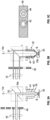
- a cylinder 29 (also referred to herein as an "attachment” or a "cylinder attachment”) can be fastened to nosepiece 23 of FMIS 100 (e.g., via screws or other fasteners), and an objective 35 (including annular darkfield channel 41 and brightfield channel 42) can be fastened to cylinder 29, above darkfield channel 41.
- a darkfield insert 51 having a ring of lights 46 e.g., LED lights 46
- cylinder 29 can be fastened into any nosepiece and to be used with any objective.
- cylinder 29 can be any suitable shape.
- the ring of lights included on darkfield insert 51 can include any suitable light that emits one or more wavelengths, and can be flexibly interchanged with another insert 51 having a ring of lights that includes a different type of light and emits a different wavelength (or set of wavelengths).
- a filter slider 52 a type of slider, with multiple emission/excitation filters F1, F2, F3...FN can be coupled to cylinder 29, below darkfield insert 51.
- filter F1 of slider 52 includes an aperture that allows the light from lights 46, when activated, to pass through unfiltered via darkfield channel 41 to a specimen.
- Filter F2 of slider 52 includes an excitation filter that allows only certain darkfield and brightfield wavelengths to reach a specimen.
- the excitation filter can include an aperture in the center, and only filter the darkfield light that reaches a specimen.
- filter F3 can include different filters for the brightfield and darkfield channels.
- the darkfield filter can be configured to filter the darkfield excitation light
- the brightfield filter can be configured as an emission filter to filter the light emitted from a specimen before it reaches one or more imaging devices.
- Slider 52 can include other suitable filters that target specific excitation wavelengths from reaching a specimen and/or target specific emission wavelengths from reaching one or more imaging devices.
- excitation and emission filters in any suitable configuration, can be used to reflect and transmit the desired illumination sources and wavelengths.
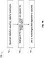
- FIG. 7A shows at a high level, an example method 700 for illuminating a specimen using a FM inspection system to achieve desired spectral emissions and other desired illumination for image capture, in accordance with some embodiments of the disclosed subject matter.
- method 700 can use FMIS 100.
- a specimen to be examined can be placed on specimen stage 30.
- the specimen is brought into focus before the light sources and filters of FMIS 100 are selected.
- control module 110 activates and adjusts one or more of the wavelengths and intensity of light from the light source(s), as well as the corresponding excitation and emission filters, according to stored information for a particular specimen, specimen class and/or any other suitable classification group.
- the stored information can include a map that identifies the type and location of known features on a specimen ("specimen feature map" or "feature map").
- the stored information can also include the material composition of a specimen, the optimal FM inspection system settings for capturing different images of the specimen at different regions of interest (e.g., by specifying the wavelength and intensity of light to direct at a specimen, by selecting and adjusting the appropriate excitation and/or emission filters). Further, the stored information can include information on type and location of known or expected defects of a specimen. Methods for selecting suitable stored information are further discussed in connection with FIG. 8 .
- Steps 720 and 730 can be repeated as many times as desired to capture different images of the specimen. For example, adjustments can be made to the intensity and wavelengths of light sources 25, 25a and/or 28 and corresponding excitation and emission filters to capture different images of the specimen. Adjustments to the light sources can be made, for example, based on stored information for a specimen, including specimen composition, known or expected defects of the specimen, and/or a specimen feature map. Further, wavelengths of light sources 25, 25a and/or 28 and corresponding filters can be adjusted for different regions of interest of the specimen (as indicated by a specimen feature map or otherwise), and images can be captured for each region of interest.
- wavelengths of light sources 25, 25a and/or 28 and corresponding filters can be selected in a range appropriate to provide desired excitation to the specimen and/or region of interest.
- different images of a specimen can be captured by adjusting the type of illumination provided to the specimen, such as, applying brightfield, darkfield, a combination of brightfield and darkfield, and/or DIC illumination.
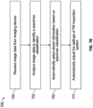
- FIG. 7B illustrates steps of an example process 705 for identifying a specimen classification and automatically adjusting the light sources and filters for FMIS 100, according to some aspects of the disclosed technology.
- Process 705 begins with step 740 which image data is received, for example, by an image processing system e.g., image processing module 834 (as shown in FIG. 8 ).
- the image data can be included in a received image of a specimen that is taken by an imaging device, as part of FMIS 100.
- the image data can include all or a portion of a specimen that is disposed on a stage of FMIS 100.
- the image data is analyzed to identify a classification of the specimen.
- image analysis may be performed to identify a subset of the specimen, such as a particular region, feature or material within the specimen.
- machine learning classifiers, computer vision, and/or artificial intelligence can be used to identify/classify the specimen and features on a specimen.
- An example classification method using convolutional neural networks (CNNs) is shown in FIG. 10 .
- stored information can be automatically selected based on the specimen (or feature) classification (step 760).
- the specimen/feature classification can be used to query a database (e.g., stored information database 836) that contains stored information associated with: a specimen, the material composition of a specimen, specimen feature types, and/or other suitable classification group.
- stored information appropriate for the specimen can be automatically identified and retrieved.
- the stored information can contain a variety of settings data that describe configurations of FMIS 100 that can be used to achieve the optimal illumination and image capture for the specimen, feature, and/or material being observed.
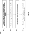
- FIG. 7C illustrates steps of an example process 710 for automatically identifying and/or classifying specimen defects, according to some aspects of the disclosed technology.
- step 780 can follow step 770 discussed above with respect to FIG. 7B .
- step 780 image data, including fluorescence, is received from the imaging device following application of adjustments/settings of the FM inspection system.
- step 780 can be performed subsequent to the automatic classification of the specimen, as describe in step 770, above.
- the image data received in step 780 can represent an image of the specimen taken under optimized or improved lighting conditions, as realized by the settings selection performed for the FM inspection system.
- the new image data including fluorescence
- a defect detection classifier that is configured to automatically identify/detect and/or classify defects/features of the specimen.
- Defect/feature detection and classification can be performed without knowledge of the specimen classification or type.
- a specimen classification and/or associated stored information can be used as inputs to the defect detection classifier, and thereby used to inform the process of defect/feature detection and identification.
- one or more defects/features of the specimen are identified and/or classified.
- the process of identifying and/or classifying specimen defects/features can be carried out in different ways, depending on the desired implementation.
- defect/feature identification can be used to automatically generate or update a feature map and/or stored information associated with the given specimen and/or specimen classification (step 795).
- identification of novel defects/features can be used to improve (train) future defect/feature classification calculations, as well as to improve the automated process of adjusting FM inspection system settings, as described in process 705.
- defect/feature identification and/or classification can be used to trigger an alert, for example to notify a user of the FM inspection system as to the existence of the detected defect/feature and/or defect/feature type (classification).
- FIG. 8 shows the general configuration of an embodiment of computer analysis system 115, in accordance with some embodiments of the disclosed subject matter.
- computer analysis system 115 is illustrated as a localized computing system in which various components are coupled via a bus 805, it is understood that various components and functional computational units (modules) can be implemented as separate physical or virtual systems.
- one or more components and/or modules can be implemented in physically separate and remote devices, such as, using virtual processes (e.g., virtual machines or containers) instantiated in a cloud environment.
- virtual processes e.g., virtual machines or containers
- Computer analysis system 115 includes a processing unit (e.g., CPU/s and/or processor/s) 810 and bus 805 that couples various system components including system memory 815, such as read only memory (ROM) 820 and random access memory (RAM) 825, to processor/s 810.
- processing unit e.g., CPU/s and/or processor/s
- bus 805 that couples various system components including system memory 815, such as read only memory (ROM) 820 and random access memory (RAM) 825, to processor/s 810.
- Memory 815 can include various memory types with different performance characteristics, such as memory cache 812.
- Processor 810 is coupled to storage device 830, which is configured to store software and instructions necessary for implementing one or more functional modules and/or database systems, such as stored information database 836.
- Each of these modules and/or database systems can be configured to control processor 810 as well as a special-purpose processor where software instructions are incorporated into the actual processor design.
- image processing module 834 and the stored information database 836 can be completely self-contained systems.
- processing module 834 can be implemented as a discrete image processing system, without departing from the scope of the disclosed technology.
- input device 845 can represent any number of input mechanisms, such as a microphone for speech, a touch-sensitive screen for gesture or graphical input, keyboard, mouse, motion input and so forth.
- An output device 835 can also be one or more of a number of output mechanisms known to those of skill in the art.
- multimodal systems can enable a user to provide multiple types of input to communicate with computer analysis system 115, for example, to convey specimen information relating to a specimen type/classification, or other characteristics.
- Communications interface 840 can generally govern and manage the user input and system output. There is no restriction on operating on any particular hardware arrangement and therefore the basic features here may easily be substituted for improved hardware or firmware arrangements as they are developed.
- Storage device 830 is a non-transitory memory and can be a hard disk or other types of computer readable media that can store data accessible by a computer, such as magnetic cassettes, flash memory cards, solid state memory devices, digital versatile disks, cartridges, random access memories (RAMs) 825, read only memory (ROM) 820, and hybrids thereof.
- RAMs random access memories
- ROM read only memory
- stored information database 836 can be configured to receive, store and update context data associated with a specimen, a specimen class and/or or other suitable specimen classification.
- Context data for each specimen/specimen class/specimen classification can include, but is not limited to: a computer aided design (CAD) file of a specimen and/or features of a specimen, a feature map identifying features and their locations, images of specimens/features of specimens caputred by FMIS 100, images of known specimens and/or features, known dimensions, material composition, mechanical and/or physical properties of a specimen, spectral variation maps for known materials or specimens, common stacking faults, structural defects or other defects associated with a specimen, optimal FM inspection settings for features of a specimen, a specimen or specimen classification, identification of regions of interest/or materials of interest to examine.
- CAD computer aided design
- Storage information database 836 can be coupled to image processing module 834 and can transmit data to and receive data from image processing module 834.
- context data can include data related to the FMIS 100 being used to inspect a specimen such as: the number of light sources, the wavelength range and intensity for each light source, the number of imaging devices and the different types of excitation/emission filters and their locations, of FMIS 100; the range of possible distances between specimen stage 30 and objective 35.
- Processor 810 can include an image processing module 834.
- Image processing module 834 can be used in conjunction with stored information database 836 to classify a specimen based on: image data, including fluorescence, received in a specimen image(s); context data retrieved from stored information database 836, and/or other received specimen characteristics, such as those manually provided by a user, for example, via input 845. Additionally, image processing module can be configured to classify specific specimen features, determine other physical and/or mechanical specimen properties (e.g., specimen reflectivity, specimen dimensions, specimen material composition). Classifications of specimen types, and specimen features/properties can be stored in stored information database 836.
- additional context data assoicated with the determined specimen type/features can be retrieved from stored information database 836 and sent to control module module 110 to adjust the settings of the FMIS 100 to capture specific specimen images and/or to guide the inspection of the specimen by FMIS 100 (e.g., by capturing images of specific features and/or regions of interest).
- an image processing module 834 can receive an entire specimen scan, or one or more images of a specimen.
- Image processing module 834 as shown in FIG. 9 , can apply one or more artificial intelligence algorithm(s) to classify a specimen type, as well as features on the specimen.
- machine learning classification schemes can utilize one or more of the following, alone or in combination: hidden Markov models; recurrent neural networks; convolutional neural networks (CNNs); deep learning; Bayesian symbolic methods; general adversarial networks; support vector machines; image registration methods; applicable rule-based system. Where regression algorithms are used, they may include including but are not limited to: a Stochastic Gradient Descent Regressor, and/or a Passive Aggressive Regressor, etc.
- Machine learning classification models can also be based on clustering algorithms (e.g., a Mini-batch K-means clustering algorithm), a recommendation algorithm (e.g., a Miniwise Hashing algorithm, or Euclidean LSH algorithm), and/or an anomaly detection algorithm, such as a Local outlier factor.
- machine learning models can employ a dimensionality reduction approach, such as, one or more of: a Mini-batch Dictionary Learning algorithm, an Incremental Principal Component Analysis (PCA) algorithm, a Latent Dirichlet Allocation algorithm, and/or a Mini-batch K-means algorithm, etc.
- PCA Incremental Principal Component Analysis
- machine learning models can be used to perform classification of
- image data from specimen images can be provided as an input to a machine learning classification system, for example, by image processing module 834.
- Classifier output specifies a sample or feature classification that can then be used to identify specific regions of interest on a specimen for further inspection by FMIS 100, and to provide instructions to control module 110 of FMIS 100 on the type of lights sources and filters that should be used to inspect those areas of interest.
- Such algorithms, networks, machines and systems provide examples of structures used with respect to any "means for determining a feature of a specimen using artificial intelligence" or "means for determining a region of interest of a specimen for further inspection using artificial intelligence” or "means for determining a feature of a specimen using artificial intelligence.”
- the image processing module can apply one or more artificial intelligence algorithm(s) to: i) detect the feature; ii) classify the feature type; iii) determine location of the feature on the specimen; iv) determine the material composition of the specimen/feature; v) determine optimal settings for FMIS 100 (e.g., the wavelength excitation setting, the wavelength emission setting, the illumination technique applied).to inspect a feature/specimen/material.
- one or more artificial intelligence algorithm(s) to: i) detect the feature; ii) classify the feature type; iii) determine location of the feature on the specimen; iv) determine the material composition of the specimen/feature; v) determine optimal settings for FMIS 100 (e.g., the wavelength excitation setting, the wavelength emission setting, the illumination technique applied).to inspect a feature/specimen/material.
- the algorithm(s) used by image processing module 834 can consider context date like location of the feature on a specimen, the type of specimen being inspected, the physical and mechanical properties of the specimen being inspected, similar features on the same or similar specimen, a reference feature map for the inspected specimen, the FM inspection system settings used to generate the specimen scan or specimen image.
- Examples of machine- learning artificial intelligence based image processing algorithm that can be used by image processing module 834 is image registration as described by: Barbara Zitova,”Image Registration Methods: A Survey,” Image and Vision Computing , October 11, 2003, Volume 21, Issue 11, pp. 977-1000 .
- the disclosed methods are just examples and are not intended to be limiting.
- machine-learning/artificial intelligence models can be trained using multiple sources of training data, including, but not limited to: a computer aided design (CAD) file of a specimen and/or features of a specimen, a specimen feature map identifying features and their locations on a specimen, images of known specimens and/or features, and/or information about known specimens (e.g., a specimen's dimensions, a speciman's material composition, the mechanical and/or physical properties of a specimen, spectral variation maps for known materials or specimens, common stacking faults, structural defects, feature maps that identify where features within a specimen classification are commonly located).
- CAD computer aided design
- an image processing algorithm 905 is first trained with training data 920 so that image processing module 834 can recognize and classify a specimen, and detect and recognize features on a specimen.
- Multiple training techniques may be used and may depend upon the particular classifier model being used.
- a CNN such as a 13-layer CNN, etc., may be trained over multiple epochs using stochastic gradient descent to explore a respective error space.
- 80 epochs are used for training and the stochastic gradient descent can include a momentum factor.
- an adaptive learning rate can be used such as, for example and without imputing limitation, an adjustment to the learning rate from 0.1 (e.g., as a step value in the stochastic gradient descent) during early epochs to 0.01 in later epochs.
- Training data 920 can include labeled examples of known types of specimens and features. For each classification being trained for (e.g., feature, feature type, type of defect, etc.), training data 920 can further include labeled imaged of deformed features (these can be actual deformed features or deformed features that were simulated according to predefined parameters) and training data 920 can include labeled images of such deformed features. Training data 920 can also include labeled images of each defect type rotated from 0-360 degrees. Training data 920 can also include labeled images of each defect type generated at different sizes. One example of training data 920 are images including labeled stacking faults having different structures, shapes and sizes, and the corresponding fluorescence emission for each type of stacking fault.
- labeled images can also include additional context data like information specifying the settings for FMIS 100 (e.g., wavelength excitation setting, wavelength emission setting, lighting technique applied), the material composition of a feature or a specimen, location of a feature on a specimen, physical/mechanical properties of the feature and/or any other suitable characteristic.
- training data can also include unlabeled data.
- image processing module 834 can be applied by image processing module 834 to a received specimen scan(s) or image(s) of a specimen to classify specimen type, detect features, classify fault type, determine feature and/or fault locations, determine specimen composition, and determine optimal FM inspection system settings for detecting a feature/specimen.
- the output data can be displayed visually, printed, or generated in file form and stored in database 836 or transmitted to other components for further processing.
- output data can be sent to a feature map generator module 832 to generate a feature map for the specimen.
- the output data may comprise multiple images.
- the generated feature map can identify and locate features on the specimen.
- the generated feature map can be displayed visually, printed, or generated in file form and stored in stored information database 836 or transmitted to other modules for further processing.
- the generated feature map can be used to focus further inspection by FMIS 100 on specific features and/or regions of a specimen.
- stored information can be retrieved from stored information database 836.
- instructions can be retrieved from stored information database 836 for applying different lights sources and illumination techniques, at different wavelengths and intensity levels, using different excitation/emission filters to capture different images and transmitted to control module 110.
- different bandpass emission filters before one or more imaging device, different fluorescence emissions can be detected and different features of a specimen identified (e.g., irregularities or defects in the surface) of a specimen.
- FIG.10 describes one embodiment for training image processing module 834 that uses a deep convolution network classifier 1005.
- Classifier 1005 can be trained using simulated augmented data 1007. For example, known defects for different types of specimens can be generated at different orientations, different sizes, different pixel intensities, different locations on a specimen (1006 and 1009). The shapes of these known defects can be blurred and/or distorted.
- one or more candidate images of FMIS 100 can be input into a classifier (1009).
- the image (1001) is first processed by detecting certain regions and extracting features from those regions (1002 and 1003). Classifier 1005 is then used to analyze the extracted features and to classify the features into types and locate those features on the specimen (1010).
- the known defects include stacking faults having different structures, sizes and shapes.
- any suitable computer readable media can be used for storing instructions for performing the functions and/or processes described herein.
- computer readable media can be transitory or non-transitory.
- non-transitory computer readable media can include media such as non-transitory magnetic media (such as hard disks, floppy disks, etc.), non-transitory optical media (such as compact discs, digital video discs, Blu-ray discs, etc.), non-transitory semiconductor media (such as flash memory, electrically programmable read only memory (EPROM), electrically erasable programmable read only memory (EEPROM), etc.), any suitable media that is not fleeting or devoid of any semblance of permanence during transmission, and/or any suitable tangible media.
- EPROM electrically programmable read only memory
- EEPROM electrically erasable programmable read only memory
- transitory computer readable media can include signals on networks, in wires, conductors, optical fibers, circuits, and any suitable media that is fleeting and devoid of any semblance of permanence during transmission, and/or any suitable intangible media.
- a cloud-based computing system is a system that provides virtualized computing resources, software and/or information to client devices.
- the computing resources, software and/or information can be virtualized by maintaining centralized services and resources that the edge devices can access over a communication interface, such as a network.
- the cloud can provide various cloud computing services via cloud elements, such as software as a service (SaaS) (e.g., collaboration services, email services, enterprise resource planning services, content services, communication services, etc.), infrastructure as a service (IaaS) (e.g., security services, networking services, systems management services, etc.), platform as a service (PaaS) (e.g., web services, streaming services, application development services, etc.), and other types of services such as desktop as a service (DaaS), information technology management as a service (ITaaS), managed software as a service (MSaaS), mobile backend as a service (MBaaS), etc.
- SaaS software as a service
- IaaS infrastructure as a service
- PaaS platform as a service
- DaaS desktop as a service
- ITaaS information technology management as a service
- MSaaS managed software as a service
- MaaS mobile backend as a service
- the present disclosure also relates to an apparatus for performing the operations herein.
- This apparatus may be specially constructed for the required purposes, or it may comprise a general-purpose computer selectively activated or reconfigured by a computer program stored on a computer readable medium that can be accessed by the computer.
- a computer program may be stored in a computer readable storage medium, such as, but is not limited to, any type of disk including floppy disks, optical disks, CD-ROMs, magnetic-optical disks, read-only memories (ROMs), random access memories (RAMs), EPROMs, EEPROMs, magnetic or optical cards, application specific integrated circuits (ASICs), or any type of non-transient computer-readable storage medium suitable for storing electronic instructions.
- the computers referred to in the specification may include a single processor or may be architectures employing multiple processor designs for increased computing capability.
Landscapes
- Physics & Mathematics (AREA)
- Engineering & Computer Science (AREA)
- General Physics & Mathematics (AREA)
- Analytical Chemistry (AREA)
- Chemical & Material Sciences (AREA)
- Multimedia (AREA)
- Optics & Photonics (AREA)
- Health & Medical Sciences (AREA)
- General Health & Medical Sciences (AREA)
- Life Sciences & Earth Sciences (AREA)
- Theoretical Computer Science (AREA)
- Molecular Biology (AREA)
- Biomedical Technology (AREA)
- Computer Vision & Pattern Recognition (AREA)
- Signal Processing (AREA)
- Pathology (AREA)
- Biochemistry (AREA)
- Immunology (AREA)
- Quality & Reliability (AREA)
- Nuclear Medicine, Radiotherapy & Molecular Imaging (AREA)
- Microscoopes, Condenser (AREA)
- Investigating, Analyzing Materials By Fluorescence Or Luminescence (AREA)
- Investigating Materials By The Use Of Optical Means Adapted For Particular Applications (AREA)
- Image Analysis (AREA)
Claims (13)
- Mikroskopiesystem, umfassend:einem Rahmen;eine oder mehrere inkohärente Lichtquellen (25, 25a, 28), die mit dem Rahmen verbunden sind und die konfiguriert sind, um mindestens eine erste Wellenlänge von Licht, die eine Probe zum Fluoreszieren veranlasst, und eine zweite Wellenlänge von Licht, die die Probe nicht zum Fluoreszieren veranlasst, zu emittieren, wobei das emittierte Licht konfiguriert ist, um auf die Probe gerichtet zu sein;einen Anregungsfilter (15), der mit dem Rahmen verbunden ist und der konfiguriert ist, um Licht von der einen oder den mehreren inkohärenten Lichtquellen zu filtern, wobei das gefilterte Licht konfiguriert ist, um einer vorbestimmten, der Probe zugehörigen Bandlückenenergie zu entsprechen;ein Objektiv (35), das mit dem Rahmen verbunden ist, wobei das Objektiv einen Hellfeldkanal (42) und einen Dunkelfeldkanal (41) umfasst;einen Objektivwechselrevolver (23), der über einen Aufsatz mit dem Objektiv verbunden ist;einen Schieber (40), der mit dem Rahmen verbunden ist und der entlang eines Strahlengangs zwischen dem Objektiv und der einen oder den mehreren inkohärenten Lichtquellen positioniert ist, wobei der Schieber mindestens eine Konfiguration einschließt, die konfiguriert ist, um Licht entlang des Stahlengangs zu mindestens dem Dunkelfeldkanal zu übertragen, der konfiguriert ist, um das Licht in einem schrägen Winkel auf die Probe zu richten;einen Emissionsfilter (18, 19), der mit dem Rahmen verbunden ist und der zum Filtern ausgewählter Wellenlängen von Licht, das von der Probe zu einer Empfangskamera reflektiert wird, konfiguriert ist; undeine Steuereinheit (110), umfassend:einen oder mehrere Prozessoren (810); undeinen Speicher (815), der Anweisungen speichert, die, als Ergebnis eines Ausführens durch den einen oder die mehreren Prozessoren, das Mikroskopiesystem veranlassen, um:Bilddaten von der Empfangskamera zu erhalten, wobei die Bilddaten auf dem gerichteten Licht basieren, das von der Probe reflektiert wird;die Probe basierend auf den empfangenen Bilddaten mit einem trainierten Klassifikator zu klassifizieren;gespeicherte Systemkonfigurationen abzurufen, die zu einer Klassifizierung der Probe zugehörig sind;die gespeicherten Systemkonfigurationen auf eine oder mehrere der inkohärenten Lichtquellen, den Anregungsfilter, den Emissionsfilter oder die Empfangskamera anzuwenden;zusätzliche Bilddaten von der Empfangskamera zu erhalten, wobei die zusätzlichen Bilddaten erhalten werden, nachdem die Systemkonfigurationen angewendet wurden;Probendefekte mit einem Bilddatenmodel zu identifizieren, das auf den erhaltenen zusätzlichen Bilddaten basiert, wobei das Bilddatenmodell ein trainierter Defekterfassungsklassifikator ist; undeine Merkmalskarte basierend auf den Probendefekten zu erzeugen.
- System nach Anspruch 1, wobei mindestens eine Konfiguration des Schiebers konfiguriert ist, um Licht sowohl zu dem Hellfeldkanal als auch zu dem Dunkelfeldkanal zu übertragen.
- System nach Anspruch 1 oder Anspruch 2, weiter umfassend mindestens ein zweite Kamera, und wobei das emittierte Licht sichtbares und nicht sichtbares Licht umfasst, das auf entsprechende Kameras gerichtet ist; und/oder weiter umfassend eine oder mehrere zusätzliche Kameras, die mit dem Rahmen verbunden sind, wobei jede zusätzliche Kamera konfiguriert ist, um entsprechende spezifische Wellenlängen von Licht zu empfangen.
- System nach Anspruch 1, Anspruch 2 oder Anspruch 3, wobei die eine oder die mehreren inkohärenten Lichtquellen weiter umfassen:eine erste Lichtquelle, die mit dem Rahmen verbunden ist und die konfiguriert ist, um reflektiertes Licht von der einen oder den mehreren inkohärenten Lichtquellen zu der Probe zu emittieren; undeine zusätzliche Lichtquelle, die unterhalb der Probe am Rahmen befestigt ist und die konfiguriert ist, um die Lichtintensität auf der Probe zu erhöhen, indem sie auf die Probe gerichtetes Licht gleichzeitig mit dem von der einen oder den mehreren inkohärenten Lichtquellen emittierten Licht emittiert.
- System nach Anspruch 1 oder nach einem der Ansprüche 2 bis 4, weiter umfassend einen Strahlteiler (20), der mit dem Rahmen verbunden ist und der konfiguriert ist, um emittiertes Licht in Richtung zu der Probe zu richten.
- Verfahren, umfassend:Emittieren von einer oder mehreren inkohärenten Lichtquellen (25, 25a, 28, 46) mindestens einer ersten Wellenlänge von Licht, die eine Probe zum Fluoreszieren veranlasst, und eine zweite Wellenlänge von Licht, die die Probe nicht zum Fluoreszieren veranlasst, wobei das emittierte Licht auf die Probe gerichtet ist;Filtern des emittierten Lichts durch einen Anregungsfilter (15, F1, F2, F3), wobei das gefilterte Licht einer vorbestimmten Bandlückenenergie entspricht;Übertragen des emittierten Lichts (40, 52) über einen Dunkelfeldkanal eines Objektivs (35) in einem schrägen Winkel durch einen Schieber zu der Probe;Richten, unter Verwendung eines Emissionsfilters (18, 19), von der Probe reflektiertes Licht auf eine Empfangskamera, wobei das gerichtete Licht, das von der Probe reflektiert wird, ausgewählte Wellenlängen umfasst;Erhalten, von der Empfangskamera, von Bilddaten, die auf dem gerichteten Licht basieren, das von der Probe reflektiert wird;Klassifizieren der Probe mit einem trainierten Klassifikator basierend auf den Bilddaten; Abrufen gespeicherter Systemkonfigurationen, die zu der Klassifizierung der Probe zugehörig sind;Anwenden der Systemkonfigurationen auf eine oder mehrere inkohärente Lichtquellen, den Anregungsfilter, den Emissionsfilter oder die Empfangskamera;Erhalten zusätzlicher Bilddaten von der Empfangskamera, wobei die zusätzlichen Bilddaten erhalten werden, nachdem die Systemkonfigurationen angewendet sind;Identifizieren von Probendefekten mit einem Bilddatenmodell, das auf den erhaltenen zusätzlichen Bilddaten basiert, wobei das Bilddatenmodell ein trainierter Defekterfassungsklassifikator ist; undErzeugen einer Merkmalskarte basierend auf den Probendefekten.
- Verfahren nach Anspruch 6, weiter umfassend ein Übertragen des gefilterten Lichts zu der Probe durch den Schieber zu einem Hellfeldkanal des Objektivs.
- Verfahren nach Anspruch 6 oder 7, wobei ein über dem Dunkelfeldkanal des Objektivs positionierter Dunkelfeldeinsatz, der einen Ring von Lichtern (46) umfasst, Licht in einem schrägen Winkel über den Dunkelfeldkanal des Objektivs zu der Probe emittiert; und/oder wobei das emittierte Licht sichtbares und nicht sichtbares Licht umfasst, und weiter umfassend ein Empfangen, durch eine zweite Kamera, mindestens eines Teils des gerichteten Lichts, das von der Probe reflektiert wird.
- Verfahren nach Anspruch 6, Anspruch 7 oder Anspruch 8, weiter umfassend ein Empfangen, durch eine oder mehrere zusätzliche Kameras, spezifischer Wellenlängen des von der Probe reflektierten Lichts.
- Verfahren nach Anspruch 6 oder nach einem der Ansprüche 7 bis 9, weiter umfassend:Emittieren eines ersten Lichts von einer ersten Lichtquelle von der einen oder den mehreren inkohärenten Lichtquellen in Richtung zu der Probe; undErhöhen einer Lichtintensität auf der Probe durch Emittieren eines zweiten Lichts, das von einer zusätzlichen Lichtquelle von der einen oder den mehreren inkohärenten Lichtquellen von unterhalb der Probe auf die Probe gerichtet ist, wobei das zusätzliche Licht gleichzeitig mit dem von der ersten Lichtquelle von der einen oder der mehreren inkohärenten Lichtquellen emittierten Licht emittiert wird.
- Verfahren nach Anspruch 6 oder nach einem der Ansprüche 7 bis 10, weiter umfassend ein Richten des emittierten Lichts in Richtung zu der Probe mit einem Strahlteiler (20).
- Mikroskopieeinrichtung, umfassend:eine oder mehrere inkohärente Lichtquellen (25, 25a, 28), die konfiguriert sind, um mindestens eine erste Wellenlänge von Licht, die eine Probe zum Fluoreszieren veranlasst, und eine zweite Wellenlänge von Licht, die die Probe nicht zum Fluoreszieren veranlasst, zu emittieren, wobei das emittierte Licht konfiguriert ist, um auf die Probe gerichtet zu sein;einen Anregungsfilter (15), der konfiguriert ist, um Licht von der einen oder den mehreren Lichtquellen zu filtern, wobei das gefilterte Licht konfiguriert ist, um einer vorbestimmten, der Probe zugehörigen Bandlückenenergie zu entsprechen;ein Objektiv (35), umfassend einen Hellfeldkanal (42) und einen Dunkelfeldkanal (41);einen Objektivwechselrevolver (23), der über einen Aufsatz mit dem Objektiv verbunden ist;einen Dunkelfeldeinsatz (51), der am Aufsatz befestigt und über dem Dunkelfeldkanal des Objektivs positioniert ist, wobei der Dunkelfeldeinsatz einen Ring von Lichtern (46) umfasst, der konfiguriert ist, um Licht in einem schrägen Winkel auf die Probe zu projizieren;einen Emissionsfilter (18, 19), der zum Filtern ausgewählter Wellenlängen des von der Probe zu einer Empfangskamera reflektierten Lichts konfiguriert ist; undeinen oder mehrere Prozessoren (810); undeinen Speicher (815), der Anweisungen speichert, die, wenn sie durch den einen oder die mehreren Prozessoren ausgeführt werden, das den einen oder die mehreren Prozessoren veranlassen, um:Bilddaten von der Empfangskamera zu empfangen, wobei die Bilddaten auf dem gerichteten Licht basieren, das von der Probe reflektiert wird;die Probe basierend auf den empfangenen Bilddaten mit einem trainierten Klassifikator zu klassifizieren; gespeicherte Systemkonfigurationen abzurufen, die zu einer Klassifizierung der Probe zugehörig sind;die Systemkonfigurationen auf eine oder mehrere der Lichtquellen, den Anregungsfilter, den Emissionsfilter oder die Empfangskamera anzuwenden;zusätzliche Bilddaten von der Empfangskamera zu empfangen, wobei die zusätzlichen Bilddaten empfangen werden, nachdem die Systemkonfigurationen angewendet wurden;Probendefekte mit einem Bilddatenmodel zu identifizieren, das auf den empfangenen zusätzlichen Bilddaten basiert, wobei das Bilddatenmodell ein trainierter Defekterfassungsklassifikator ist; undeine Merkmalskarte basierend auf den Probendefekten zu erzeugen.
- Mikroskopieeinrichtung nach Anspruch 12, weiter umfassend einen Filterschieber (52), der unterhalb des Dunkelfeldeinsatzes (51) positioniert ist, wobei der Filterschieber konfiguriert ist, um mehrere Typen von Anregungsfiltern bereitzustellen; und einen oder mehrere zusätzliche Emissionsfilter für einen oder mehrere von dem Hellfeldkanal oder dem Dunkelfeldkanal.
Priority Applications (1)
| Application Number | Priority Date | Filing Date | Title |
|---|---|---|---|
| EP25168435.3A EP4557759A3 (de) | 2019-02-07 | 2020-02-04 | Fluoreszenzmikroskopieinspektionssysteme, -vorrichtung und -verfahren |
Applications Claiming Priority (3)
| Application Number | Priority Date | Filing Date | Title |
|---|---|---|---|
| US201962802246P | 2019-02-07 | 2019-02-07 | |
| US16/399,058 US10578850B1 (en) | 2019-02-07 | 2019-04-30 | Fluorescence microscopy inspection systems, apparatus and methods |
| PCT/US2020/016497 WO2020163267A1 (en) | 2019-02-07 | 2020-02-04 | Fluorescence microscopy inspection systems, apparatus and methods |
Related Child Applications (2)
| Application Number | Title | Priority Date | Filing Date |
|---|---|---|---|
| EP25168435.3A Division EP4557759A3 (de) | 2019-02-07 | 2020-02-04 | Fluoreszenzmikroskopieinspektionssysteme, -vorrichtung und -verfahren |
| EP25168435.3A Division-Into EP4557759A3 (de) | 2019-02-07 | 2020-02-04 | Fluoreszenzmikroskopieinspektionssysteme, -vorrichtung und -verfahren |
Publications (3)
| Publication Number | Publication Date |
|---|---|
| EP3909236A1 EP3909236A1 (de) | 2021-11-17 |
| EP3909236A4 EP3909236A4 (de) | 2022-10-12 |
| EP3909236B1 true EP3909236B1 (de) | 2025-05-14 |
Family
ID=71944815
Family Applications (2)
| Application Number | Title | Priority Date | Filing Date |
|---|---|---|---|
| EP25168435.3A Pending EP4557759A3 (de) | 2019-02-07 | 2020-02-04 | Fluoreszenzmikroskopieinspektionssysteme, -vorrichtung und -verfahren |
| EP20753126.0A Active EP3909236B1 (de) | 2019-02-07 | 2020-02-04 | Systeme, vorrichtung und verfahren zur inspektion von fluoreszenzmikroskopie |
Family Applications Before (1)
| Application Number | Title | Priority Date | Filing Date |
|---|---|---|---|
| EP25168435.3A Pending EP4557759A3 (de) | 2019-02-07 | 2020-02-04 | Fluoreszenzmikroskopieinspektionssysteme, -vorrichtung und -verfahren |
Country Status (6)
| Country | Link |
|---|---|
| US (3) | US11294162B2 (de) |
| EP (2) | EP4557759A3 (de) |
| JP (2) | JP7226856B2 (de) |
| KR (2) | KR102911716B1 (de) |
| CN (1) | CN113412613B (de) |
| WO (1) | WO2020163267A1 (de) |
Families Citing this family (18)
| Publication number | Priority date | Publication date | Assignee | Title |
|---|---|---|---|---|
| CN113646877B (zh) * | 2019-03-28 | 2023-08-18 | 浜松光子学株式会社 | 检查装置及检查方法 |
| WO2021067726A1 (en) * | 2019-10-03 | 2021-04-08 | The Regents Of The University Of California | Fluorescence imitating brightfield imaging |
| EP4027182B1 (de) | 2021-01-08 | 2024-10-30 | Leica Microsystems CMS GmbH | Lichtwand-fluoreszenzmikroskopie für eine vielzahl von proben |
| JP7238041B2 (ja) * | 2021-07-29 | 2023-03-13 | キヤノン株式会社 | 計測装置、計測方法、基板処理装置、および物品の製造方法 |
| EP4198604B1 (de) * | 2021-12-17 | 2025-10-29 | Thermo Electron Scientific Instruments LLC | Verfahren und system zur positionierung einer probe |
| CN114295565B (zh) * | 2021-12-28 | 2023-08-08 | 上海集成电路装备材料产业创新中心有限公司 | 测定图像传感器量子效率的方法、装置、设备和介质 |
| CN114581782B (zh) * | 2022-05-06 | 2022-08-16 | 南京航空航天大学 | 一种基于由粗到精检测策略的细微缺陷检测方法 |
| CN115825076B (zh) * | 2022-11-07 | 2024-05-28 | 睿励科学仪器(上海)有限公司 | 一种缺陷检测装置和检测方法 |
| KR102946366B1 (ko) * | 2022-12-07 | 2026-04-01 | (주)넥스틴 | 실시간 가변 기능을 갖는 암시야 검사 장치 |
| WO2024134240A1 (en) * | 2022-12-20 | 2024-06-27 | Bit Group France | Optical flow cytometer for fluorescence and scattering measurements by segmentation of beam emitted by a single non-coherent light source |
| US12561788B2 (en) * | 2022-12-27 | 2026-02-24 | Samsung Electronics Co., Ltd. | Fluorescence microscopy metrology system and method of operating fluorescence microscopy metrology system |
| KR20240135295A (ko) * | 2023-03-03 | 2024-09-10 | 삼성전자주식회사 | 측정 장비 및 이를 이용하는 측정 방법. |
| CN116429766A (zh) * | 2023-03-23 | 2023-07-14 | 长园视觉科技(珠海)有限公司 | 基于多通道分离的方法、系统、装置及存储介质 |
| KR102674967B1 (ko) * | 2023-04-24 | 2024-06-13 | 주식회사 큐리오시스 | 다채널 형광 필터세트와 광원이 합쳐진 형광 필터블록 조립체 |
| WO2025144684A1 (en) * | 2023-12-28 | 2025-07-03 | Nanotronics Imaging, Inc. | Fluorescence microscopy inspection systems, apparatus and methods |
| CN117492161B (zh) * | 2023-12-29 | 2024-04-12 | 深圳市迈腾电子有限公司 | 均光片定位与纠偏方法、电子设备与计算机可读介质 |
| CN118032806A (zh) * | 2024-01-31 | 2024-05-14 | 清软微视(杭州)科技有限公司 | 暗场缺陷检测装置 |
| KR102900483B1 (ko) * | 2024-03-19 | 2025-12-16 | 한국표준과학연구원 | 색선별 거울 없이 형광 이미지를 획득할 수 있는 명암시야 현미경 |
Family Cites Families (56)
| Publication number | Priority date | Publication date | Assignee | Title |
|---|---|---|---|---|
| JPH03266809A (ja) * | 1990-03-16 | 1991-11-27 | Mitsutoyo Corp | 紫外域用落射蛍光顕微鏡 |
| JPH0537650A (ja) | 1991-07-31 | 1993-02-12 | Ricos:Kk | 音声応答装置 |
| JPH08145888A (ja) * | 1994-11-16 | 1996-06-07 | Olympus Optical Co Ltd | 蛍光測色装置 |
| JP3526489B2 (ja) * | 1995-05-25 | 2004-05-17 | オリンパス株式会社 | 落射蛍光顕微鏡 |
| JP3445722B2 (ja) * | 1997-05-14 | 2003-09-08 | 出光石油化学株式会社 | 表面検査装置および表面検査方法 |
| US6259807B1 (en) | 1997-05-14 | 2001-07-10 | Applied Imaging Corp. | Identification of objects of interest using multiple illumination schemes and finding overlap of features in corresponding multiple images |
| JP2000162134A (ja) * | 1998-12-01 | 2000-06-16 | Nidek Co Ltd | 表面検査装置 |
| JP2000283931A (ja) * | 1999-03-30 | 2000-10-13 | Idemitsu Petrochem Co Ltd | 表面検査装置および表面検査方法 |
| KR100806023B1 (ko) * | 2000-03-24 | 2008-02-26 | 올림푸스 가부시키가이샤 | 현미경 장치 |
| JP2002202459A (ja) * | 2000-12-28 | 2002-07-19 | Yoshihiro Ota | 暗視野落射顕微鏡 |
| US20040207836A1 (en) | 2002-09-27 | 2004-10-21 | Rajeshwar Chhibber | High dynamic range optical inspection system and method |
| US7027143B1 (en) * | 2002-10-15 | 2006-04-11 | Kla-Tencor Technologies Corp. | Methods and systems for inspecting reticles using aerial imaging at off-stepper wavelengths |
| US7525659B2 (en) * | 2003-01-15 | 2009-04-28 | Negevtech Ltd. | System for detection of water defects |
| JP2004290234A (ja) * | 2003-03-25 | 2004-10-21 | Shiseido Co Ltd | 皮膚の蛍光測定方法およびその装置 |
| CN100514044C (zh) | 2003-11-28 | 2009-07-15 | 财团法人工业技术研究院 | 多重反射荧光探头 |
| CN102156346B (zh) * | 2005-02-21 | 2012-07-18 | 奥林巴斯株式会社 | 微弱光标本摄像单元及微弱光标本摄像装置 |
| TWI439684B (zh) | 2005-07-06 | 2014-06-01 | Nanometrics Inc | 具自晶圓或其他工件特定材料層所發射光致發光信號優先偵測之光致發光成像 |
| US7532314B1 (en) * | 2005-07-14 | 2009-05-12 | Battelle Memorial Institute | Systems and methods for biological and chemical detection |
| JP4778755B2 (ja) * | 2005-09-09 | 2011-09-21 | 株式会社日立ハイテクノロジーズ | 欠陥検査方法及びこれを用いた装置 |
| JP4723362B2 (ja) | 2005-11-29 | 2011-07-13 | 株式会社日立ハイテクノロジーズ | 光学式検査装置及びその方法 |
| JP2008116405A (ja) * | 2006-11-07 | 2008-05-22 | Hitachi High-Technologies Corp | 欠陥検査方法及びその装置 |
| JP4936867B2 (ja) | 2006-12-05 | 2012-05-23 | 株式会社キーエンス | 拡大画像観察装置、拡大画像観察方法 |
| CA2698545C (en) | 2007-09-07 | 2014-07-08 | Fluidigm Corporation | Copy number variation determination, methods and systems |
| CN102089616B (zh) * | 2008-06-03 | 2013-03-13 | 焕·J·郑 | 干涉缺陷检测和分类 |
| JP5387328B2 (ja) | 2009-08-31 | 2014-01-15 | ソニー株式会社 | 蛍光像取得装置、蛍光像取得方法及び蛍光像取得プログラム |
| US9035267B2 (en) * | 2010-01-04 | 2015-05-19 | Bt Imaging Pty Ltd | In-line photoluminescence imaging of semiconductor devices |
| SG184961A1 (en) * | 2010-04-28 | 2012-11-29 | Kla Tencor Corp | Ring light illuminator and beam shaper for ring light illuminator |
| US9163987B2 (en) | 2010-08-24 | 2015-10-20 | Kla-Tencor Corporation | Defect inspection and photoluminescence measurement system |
| US8947777B2 (en) | 2011-02-25 | 2015-02-03 | Utah State University Research Foundation | Multiple petal deployable telescope |
| CN103140788A (zh) | 2011-09-30 | 2013-06-05 | 三洋电机株式会社 | 分束器以及观察装置 |
| US20130260382A1 (en) | 2012-02-21 | 2013-10-03 | Inscopix, Inc. | Systems and methods for utilizing microscopy |
| US9575304B2 (en) | 2012-06-25 | 2017-02-21 | Huron Technologies International Inc. | Pathology slide scanners for fluorescence and brightfield imaging and method of operation |
| CN109387494B (zh) * | 2012-07-06 | 2023-01-24 | Bt成像股份有限公司 | 检查半导体材料的方法与分析半导体材料的方法和系统 |
| JP6108772B2 (ja) | 2012-11-05 | 2017-04-05 | オリンパス株式会社 | 顕微鏡及び暗視野対物レンズ |
| HK1221135A1 (zh) * | 2013-09-18 | 2017-05-26 | 伊鲁米吉有限公司 | 光学窥器 |
| US10317347B2 (en) | 2013-11-01 | 2019-06-11 | Kla-Tencor Corp. | Determining information for defects on wafers |
| WO2015105831A1 (en) * | 2014-01-08 | 2015-07-16 | Colorado Seminary, Which Owns And Operates The University Of Denver | A wavelength dispersive microscope spectrofluorometer for characterizing multiple particles simultaneously |
| WO2015175433A1 (en) | 2014-05-12 | 2015-11-19 | Cellomics, Inc. | Automated imaging of chromophore labeled samples |
| US10437034B2 (en) | 2014-10-14 | 2019-10-08 | Nanotronics Imaging, Inc. | Unique oblique lighting technique using a brightfield darkfield objective and imaging method relating thereto |
| JP6555680B2 (ja) | 2015-01-26 | 2019-08-07 | オリンパス株式会社 | 顕微鏡用照明装置 |
| HK1246401A1 (zh) * | 2015-03-13 | 2018-09-07 | Genea Ip Holdings Pty Limited | 用於显微镜的方法及设备 |
| WO2016201177A1 (en) | 2015-06-12 | 2016-12-15 | Techshot, Inc. | Integrated illuminator and condenser for microscopes |
| US9567159B2 (en) | 2015-07-10 | 2017-02-14 | Triton Manufacturing, Inc. | Method and apparatus for constructing steel garbage dumpsters |
| US10067072B2 (en) * | 2015-07-10 | 2018-09-04 | Kla-Tencor Corporation | Methods and apparatus for speckle suppression in laser dark-field systems |
| DE102016109945A1 (de) * | 2015-11-05 | 2017-05-11 | Leica Microsystems Cms Gmbh | Mikroskop für die Durchlicht- und Fluoreszenzmikroskopie |
| US10360477B2 (en) * | 2016-01-11 | 2019-07-23 | Kla-Tencor Corp. | Accelerating semiconductor-related computations using learning based models |
| US10346740B2 (en) * | 2016-06-01 | 2019-07-09 | Kla-Tencor Corp. | Systems and methods incorporating a neural network and a forward physical model for semiconductor applications |
| US11580398B2 (en) | 2016-10-14 | 2023-02-14 | KLA-Tenor Corp. | Diagnostic systems and methods for deep learning models configured for semiconductor applications |
| US10234402B2 (en) | 2017-01-05 | 2019-03-19 | Kla-Tencor Corporation | Systems and methods for defect material classification |
| JP7029821B2 (ja) | 2017-02-10 | 2022-03-04 | ナノトロニクス イメージング インコーポレイテッド | 顕微鏡検査において大面積の撮像を容易にするためのカメラと検体の整列 |
| US11067784B2 (en) | 2017-05-01 | 2021-07-20 | Bae Systems Information And Electronic Systems Integration Inc. | System and techniques for detecting fluorescing particles on a target |
| WO2018229709A1 (en) | 2017-06-14 | 2018-12-20 | Camtek Ltd. | Automatic defect classification |
| US10146041B1 (en) | 2018-05-01 | 2018-12-04 | Nanotronics Imaging, Inc. | Systems, devices and methods for automatic microscope focus |
| CN108956507B (zh) * | 2018-09-20 | 2024-03-01 | 河南农业大学 | 叶绿素光谱检测仪 |
| US10578850B1 (en) | 2019-02-07 | 2020-03-03 | Nanotronics Imaging, Inc. | Fluorescence microscopy inspection systems, apparatus and methods |
| US20240126063A1 (en) | 2019-02-07 | 2024-04-18 | Nanotronics Imaging, Inc. | Fluorescence microscopy inspection systems, apparatus and methods |
-
2020
- 2020-01-24 US US16/751,303 patent/US11294162B2/en active Active
- 2020-02-04 EP EP25168435.3A patent/EP4557759A3/de active Pending
- 2020-02-04 KR KR1020247019632A patent/KR102911716B1/ko active Active
- 2020-02-04 WO PCT/US2020/016497 patent/WO2020163267A1/en not_active Ceased
- 2020-02-04 EP EP20753126.0A patent/EP3909236B1/de active Active
- 2020-02-04 JP JP2021545880A patent/JP7226856B2/ja active Active
- 2020-02-04 CN CN202080013058.3A patent/CN113412613B/zh active Active
- 2020-02-04 KR KR1020217027949A patent/KR102675890B1/ko active Active
-
2022
- 2022-04-04 US US17/657,818 patent/US11662563B2/en active Active
-
2023
- 2023-02-02 JP JP2023014840A patent/JP2023052870A/ja active Pending
- 2023-05-26 US US18/324,317 patent/US12298489B2/en active Active
Also Published As
| Publication number | Publication date |
|---|---|
| EP3909236A4 (de) | 2022-10-12 |
| EP4557759A2 (de) | 2025-05-21 |
| US20230296872A1 (en) | 2023-09-21 |
| US20220221703A1 (en) | 2022-07-14 |
| JP7226856B2 (ja) | 2023-02-21 |
| KR102911716B1 (ko) | 2026-01-12 |
| US11662563B2 (en) | 2023-05-30 |
| KR102675890B1 (ko) | 2024-06-14 |
| US11294162B2 (en) | 2022-04-05 |
| CN113412613A (zh) | 2021-09-17 |
| JP2022520542A (ja) | 2022-03-31 |
| EP3909236A1 (de) | 2021-11-17 |
| JP2023052870A (ja) | 2023-04-12 |
| KR20240096890A (ko) | 2024-06-26 |
| EP4557759A3 (de) | 2025-08-20 |
| KR20210122293A (ko) | 2021-10-08 |
| WO2020163267A1 (en) | 2020-08-13 |
| US12298489B2 (en) | 2025-05-13 |
| CN113412613B (zh) | 2024-01-09 |
| US20200257100A1 (en) | 2020-08-13 |
Similar Documents
| Publication | Publication Date | Title |
|---|---|---|
| EP3909236B1 (de) | Systeme, vorrichtung und verfahren zur inspektion von fluoreszenzmikroskopie | |
| US10578850B1 (en) | Fluorescence microscopy inspection systems, apparatus and methods | |
| KR102539921B1 (ko) | 자동으로 생성된 결함 피처를 가진 반도체 구조의 검사를 위한 방법 및 시스템 | |
| US20240126063A1 (en) | Fluorescence microscopy inspection systems, apparatus and methods | |
| US11995802B2 (en) | System, method and apparatus for macroscopic inspection of reflective specimens | |
| US20220383480A1 (en) | Macro inspection systems, apparatus and methods | |
| TWI821499B (zh) | 檢測系統及用於對度量衡缺陷分段之方法 | |
| TWI834005B (zh) | 干擾過濾之深度學習網路 | |
| KR102495449B1 (ko) | 다중 산란 신호에 기초한 매립된 파티클 깊이 비닝 | |
| TW202407331A (zh) | 多模式光學檢測 | |
| WO2025144684A1 (en) | Fluorescence microscopy inspection systems, apparatus and methods |
Legal Events
| Date | Code | Title | Description |
|---|---|---|---|
| STAA | Information on the status of an ep patent application or granted ep patent |
Free format text: STATUS: THE INTERNATIONAL PUBLICATION HAS BEEN MADE |
|
| PUAI | Public reference made under article 153(3) epc to a published international application that has entered the european phase |
Free format text: ORIGINAL CODE: 0009012 |
|
| STAA | Information on the status of an ep patent application or granted ep patent |
Free format text: STATUS: REQUEST FOR EXAMINATION WAS MADE |
|
| 17P | Request for examination filed |
Effective date: 20210813 |
|
| AK | Designated contracting states |
Kind code of ref document: A1 Designated state(s): AL AT BE BG CH CY CZ DE DK EE ES FI FR GB GR HR HU IE IS IT LI LT LU LV MC MK MT NL NO PL PT RO RS SE SI SK SM TR |
|
| DAV | Request for validation of the european patent (deleted) | ||
| DAX | Request for extension of the european patent (deleted) | ||
| A4 | Supplementary search report drawn up and despatched |
Effective date: 20220912 |
|
| RIC1 | Information provided on ipc code assigned before grant |
Ipc: G01N 21/88 20060101ALI20220906BHEP Ipc: G01N 21/64 20060101ALI20220906BHEP Ipc: G02B 21/00 20060101ALI20220906BHEP Ipc: G06V 20/69 20220101ALI20220906BHEP Ipc: G06T 7/00 20170101ALI20220906BHEP Ipc: G02B 21/18 20060101ALI20220906BHEP Ipc: H04N 5/247 20060101ALI20220906BHEP Ipc: G06K 9/00 20060101ALI20220906BHEP Ipc: G02B 21/36 20060101ALI20220906BHEP Ipc: G02B 21/10 20060101ALI20220906BHEP Ipc: G02B 21/12 20060101ALI20220906BHEP Ipc: G02B 21/16 20060101ALI20220906BHEP Ipc: H04N 7/18 20060101AFI20220906BHEP |
|
| GRAP | Despatch of communication of intention to grant a patent |
Free format text: ORIGINAL CODE: EPIDOSNIGR1 |
|
| STAA | Information on the status of an ep patent application or granted ep patent |
Free format text: STATUS: GRANT OF PATENT IS INTENDED |
|
| RIC1 | Information provided on ipc code assigned before grant |
Ipc: H04N 23/90 20230101ALI20241115BHEP Ipc: G01N 21/88 20060101ALI20241115BHEP Ipc: G01N 21/64 20060101ALI20241115BHEP Ipc: G02B 21/00 20060101ALI20241115BHEP Ipc: G06V 20/69 20220101ALI20241115BHEP Ipc: G06T 7/00 20170101ALI20241115BHEP Ipc: G02B 21/18 20060101ALI20241115BHEP Ipc: G02B 21/36 20060101ALI20241115BHEP Ipc: G02B 21/10 20060101ALI20241115BHEP Ipc: G02B 21/12 20060101ALI20241115BHEP Ipc: G02B 21/16 20060101ALI20241115BHEP Ipc: H04N 7/18 20060101AFI20241115BHEP |
|
| INTG | Intention to grant announced |
Effective date: 20241202 |
|
| RAP3 | Party data changed (applicant data changed or rights of an application transferred) |
Owner name: NANOTRONICS IMAGING, INC. |
|
| GRAS | Grant fee paid |
Free format text: ORIGINAL CODE: EPIDOSNIGR3 |
|
| GRAA | (expected) grant |
Free format text: ORIGINAL CODE: 0009210 |
|
| STAA | Information on the status of an ep patent application or granted ep patent |
Free format text: STATUS: THE PATENT HAS BEEN GRANTED |
|
| AK | Designated contracting states |
Kind code of ref document: B1 Designated state(s): AL AT BE BG CH CY CZ DE DK EE ES FI FR GB GR HR HU IE IS IT LI LT LU LV MC MK MT NL NO PL PT RO RS SE SI SK SM TR |
|
| REG | Reference to a national code |
Ref country code: GB Ref legal event code: FG4D |
|
| REG | Reference to a national code |
Ref country code: CH Ref legal event code: EP |
|
| REG | Reference to a national code |
Ref country code: IE Ref legal event code: FG4D |
|
| REG | Reference to a national code |
Ref country code: DE Ref legal event code: R096 Ref document number: 602020051288 Country of ref document: DE |
|
| REG | Reference to a national code |
Ref country code: NL Ref legal event code: MP Effective date: 20250514 |
|
| P01 | Opt-out of the competence of the unified patent court (upc) registered |
Free format text: CASE NUMBER: UPC_APP_5133_3909236/2025 Effective date: 20250829 |
|
| PG25 | Lapsed in a contracting state [announced via postgrant information from national office to epo] |
Ref country code: PT Free format text: LAPSE BECAUSE OF FAILURE TO SUBMIT A TRANSLATION OF THE DESCRIPTION OR TO PAY THE FEE WITHIN THE PRESCRIBED TIME-LIMIT Effective date: 20250915 Ref country code: ES Free format text: LAPSE BECAUSE OF FAILURE TO SUBMIT A TRANSLATION OF THE DESCRIPTION OR TO PAY THE FEE WITHIN THE PRESCRIBED TIME-LIMIT Effective date: 20250514 Ref country code: FI Free format text: LAPSE BECAUSE OF FAILURE TO SUBMIT A TRANSLATION OF THE DESCRIPTION OR TO PAY THE FEE WITHIN THE PRESCRIBED TIME-LIMIT Effective date: 20250514 |
|
| REG | Reference to a national code |
Ref country code: LT Ref legal event code: MG9D |
|
| PG25 | Lapsed in a contracting state [announced via postgrant information from national office to epo] |
Ref country code: NO Free format text: LAPSE BECAUSE OF FAILURE TO SUBMIT A TRANSLATION OF THE DESCRIPTION OR TO PAY THE FEE WITHIN THE PRESCRIBED TIME-LIMIT Effective date: 20250814 Ref country code: GR Free format text: LAPSE BECAUSE OF FAILURE TO SUBMIT A TRANSLATION OF THE DESCRIPTION OR TO PAY THE FEE WITHIN THE PRESCRIBED TIME-LIMIT Effective date: 20250815 |
|
| PG25 | Lapsed in a contracting state [announced via postgrant information from national office to epo] |
Ref country code: PL Free format text: LAPSE BECAUSE OF FAILURE TO SUBMIT A TRANSLATION OF THE DESCRIPTION OR TO PAY THE FEE WITHIN THE PRESCRIBED TIME-LIMIT Effective date: 20250514 Ref country code: NL Free format text: LAPSE BECAUSE OF FAILURE TO SUBMIT A TRANSLATION OF THE DESCRIPTION OR TO PAY THE FEE WITHIN THE PRESCRIBED TIME-LIMIT Effective date: 20250514 |
|
| REG | Reference to a national code |
Ref country code: AT Ref legal event code: MK05 Ref document number: 1795799 Country of ref document: AT Kind code of ref document: T Effective date: 20250514 |
|
| PG25 | Lapsed in a contracting state [announced via postgrant information from national office to epo] |
Ref country code: BG Free format text: LAPSE BECAUSE OF FAILURE TO SUBMIT A TRANSLATION OF THE DESCRIPTION OR TO PAY THE FEE WITHIN THE PRESCRIBED TIME-LIMIT Effective date: 20250514 |
|
| PG25 | Lapsed in a contracting state [announced via postgrant information from national office to epo] |
Ref country code: HR Free format text: LAPSE BECAUSE OF FAILURE TO SUBMIT A TRANSLATION OF THE DESCRIPTION OR TO PAY THE FEE WITHIN THE PRESCRIBED TIME-LIMIT Effective date: 20250514 |
|
| PG25 | Lapsed in a contracting state [announced via postgrant information from national office to epo] |
Ref country code: AT Free format text: LAPSE BECAUSE OF FAILURE TO SUBMIT A TRANSLATION OF THE DESCRIPTION OR TO PAY THE FEE WITHIN THE PRESCRIBED TIME-LIMIT Effective date: 20250514 |
|
| PG25 | Lapsed in a contracting state [announced via postgrant information from national office to epo] |
Ref country code: RS Free format text: LAPSE BECAUSE OF FAILURE TO SUBMIT A TRANSLATION OF THE DESCRIPTION OR TO PAY THE FEE WITHIN THE PRESCRIBED TIME-LIMIT Effective date: 20250814 |
|
| PG25 | Lapsed in a contracting state [announced via postgrant information from national office to epo] |
Ref country code: IS Free format text: LAPSE BECAUSE OF FAILURE TO SUBMIT A TRANSLATION OF THE DESCRIPTION OR TO PAY THE FEE WITHIN THE PRESCRIBED TIME-LIMIT Effective date: 20250914 |
|
| PG25 | Lapsed in a contracting state [announced via postgrant information from national office to epo] |
Ref country code: LV Free format text: LAPSE BECAUSE OF FAILURE TO SUBMIT A TRANSLATION OF THE DESCRIPTION OR TO PAY THE FEE WITHIN THE PRESCRIBED TIME-LIMIT Effective date: 20250514 |
|
| PG25 | Lapsed in a contracting state [announced via postgrant information from national office to epo] |
Ref country code: SM Free format text: LAPSE BECAUSE OF FAILURE TO SUBMIT A TRANSLATION OF THE DESCRIPTION OR TO PAY THE FEE WITHIN THE PRESCRIBED TIME-LIMIT Effective date: 20250514 Ref country code: DK Free format text: LAPSE BECAUSE OF FAILURE TO SUBMIT A TRANSLATION OF THE DESCRIPTION OR TO PAY THE FEE WITHIN THE PRESCRIBED TIME-LIMIT Effective date: 20250514 |
|
| PG25 | Lapsed in a contracting state [announced via postgrant information from national office to epo] |
Ref country code: CZ Free format text: LAPSE BECAUSE OF FAILURE TO SUBMIT A TRANSLATION OF THE DESCRIPTION OR TO PAY THE FEE WITHIN THE PRESCRIBED TIME-LIMIT Effective date: 20250514 |
|
| PG25 | Lapsed in a contracting state [announced via postgrant information from national office to epo] |
Ref country code: EE Free format text: LAPSE BECAUSE OF FAILURE TO SUBMIT A TRANSLATION OF THE DESCRIPTION OR TO PAY THE FEE WITHIN THE PRESCRIBED TIME-LIMIT Effective date: 20250514 |
|
| PG25 | Lapsed in a contracting state [announced via postgrant information from national office to epo] |
Ref country code: SK Free format text: LAPSE BECAUSE OF FAILURE TO SUBMIT A TRANSLATION OF THE DESCRIPTION OR TO PAY THE FEE WITHIN THE PRESCRIBED TIME-LIMIT Effective date: 20250514 Ref country code: RO Free format text: LAPSE BECAUSE OF FAILURE TO SUBMIT A TRANSLATION OF THE DESCRIPTION OR TO PAY THE FEE WITHIN THE PRESCRIBED TIME-LIMIT Effective date: 20250514 |
|
| PG25 | Lapsed in a contracting state [announced via postgrant information from national office to epo] |
Ref country code: IT Free format text: LAPSE BECAUSE OF FAILURE TO SUBMIT A TRANSLATION OF THE DESCRIPTION OR TO PAY THE FEE WITHIN THE PRESCRIBED TIME-LIMIT Effective date: 20250514 |
|
| REG | Reference to a national code |
Ref country code: DE Ref legal event code: R097 Ref document number: 602020051288 Country of ref document: DE |
|
| PLBE | No opposition filed within time limit |
Free format text: ORIGINAL CODE: 0009261 |
|
| STAA | Information on the status of an ep patent application or granted ep patent |
Free format text: STATUS: NO OPPOSITION FILED WITHIN TIME LIMIT |
|
| REG | Reference to a national code |
Ref country code: CH Ref legal event code: L10 Free format text: ST27 STATUS EVENT CODE: U-0-0-L10-L00 (AS PROVIDED BY THE NATIONAL OFFICE) Effective date: 20260325 |
|
| PGFP | Annual fee paid to national office [announced via postgrant information from national office to epo] |
Ref country code: DE Payment date: 20260326 Year of fee payment: 7 |
|
| PGFP | Annual fee paid to national office [announced via postgrant information from national office to epo] |
Ref country code: FR Payment date: 20260325 Year of fee payment: 7 |
|
| 26N | No opposition filed |
Effective date: 20260217 |