EP3905331B1 - Dispositif d'affichage et son procédé de réparation - Google Patents
Dispositif d'affichage et son procédé de réparation Download PDFInfo
- Publication number
- EP3905331B1 EP3905331B1 EP19905505.4A EP19905505A EP3905331B1 EP 3905331 B1 EP3905331 B1 EP 3905331B1 EP 19905505 A EP19905505 A EP 19905505A EP 3905331 B1 EP3905331 B1 EP 3905331B1
- Authority
- EP
- European Patent Office
- Prior art keywords
- electrode
- light emitting
- rel2
- rel1
- emitting elements
- Prior art date
- Legal status (The legal status is an assumption and is not a legal conclusion. Google has not performed a legal analysis and makes no representation as to the accuracy of the status listed.)
- Active
Links
Images


Classifications
-
- H—ELECTRICITY
- H10—SEMICONDUCTOR DEVICES; ELECTRIC SOLID-STATE DEVICES NOT OTHERWISE PROVIDED FOR
- H10H—INORGANIC LIGHT-EMITTING SEMICONDUCTOR DEVICES HAVING POTENTIAL BARRIERS
- H10H29/00—Integrated devices, or assemblies of multiple devices, comprising at least one light-emitting semiconductor element covered by group H10H20/00
- H10H29/10—Integrated devices comprising at least one light-emitting semiconductor component covered by group H10H20/00
- H10H29/14—Integrated devices comprising at least one light-emitting semiconductor component covered by group H10H20/00 comprising multiple light-emitting semiconductor components
- H10H29/142—Two-dimensional arrangements, e.g. asymmetric LED layout
-
- G—PHYSICS
- G09—EDUCATION; CRYPTOGRAPHY; DISPLAY; ADVERTISING; SEALS
- G09G—ARRANGEMENTS OR CIRCUITS FOR CONTROL OF INDICATING DEVICES USING STATIC MEANS TO PRESENT VARIABLE INFORMATION
- G09G3/00—Control arrangements or circuits, of interest only in connection with visual indicators other than cathode-ray tubes
- G09G3/20—Control arrangements or circuits, of interest only in connection with visual indicators other than cathode-ray tubes for presentation of an assembly of a number of characters, e.g. a page, by composing the assembly by combination of individual elements arranged in a matrix no fixed position being assigned to or needed to be assigned to the individual characters or partial characters
- G09G3/22—Control arrangements or circuits, of interest only in connection with visual indicators other than cathode-ray tubes for presentation of an assembly of a number of characters, e.g. a page, by composing the assembly by combination of individual elements arranged in a matrix no fixed position being assigned to or needed to be assigned to the individual characters or partial characters using controlled light sources
- G09G3/30—Control arrangements or circuits, of interest only in connection with visual indicators other than cathode-ray tubes for presentation of an assembly of a number of characters, e.g. a page, by composing the assembly by combination of individual elements arranged in a matrix no fixed position being assigned to or needed to be assigned to the individual characters or partial characters using controlled light sources using electroluminescent panels
- G09G3/32—Control arrangements or circuits, of interest only in connection with visual indicators other than cathode-ray tubes for presentation of an assembly of a number of characters, e.g. a page, by composing the assembly by combination of individual elements arranged in a matrix no fixed position being assigned to or needed to be assigned to the individual characters or partial characters using controlled light sources using electroluminescent panels semiconductive, e.g. using light-emitting diodes [LED]
- G09G3/3208—Control arrangements or circuits, of interest only in connection with visual indicators other than cathode-ray tubes for presentation of an assembly of a number of characters, e.g. a page, by composing the assembly by combination of individual elements arranged in a matrix no fixed position being assigned to or needed to be assigned to the individual characters or partial characters using controlled light sources using electroluminescent panels semiconductive, e.g. using light-emitting diodes [LED] organic, e.g. using organic light-emitting diodes [OLED]
- G09G3/3225—Control arrangements or circuits, of interest only in connection with visual indicators other than cathode-ray tubes for presentation of an assembly of a number of characters, e.g. a page, by composing the assembly by combination of individual elements arranged in a matrix no fixed position being assigned to or needed to be assigned to the individual characters or partial characters using controlled light sources using electroluminescent panels semiconductive, e.g. using light-emitting diodes [LED] organic, e.g. using organic light-emitting diodes [OLED] using an active matrix
- G09G3/3233—Control arrangements or circuits, of interest only in connection with visual indicators other than cathode-ray tubes for presentation of an assembly of a number of characters, e.g. a page, by composing the assembly by combination of individual elements arranged in a matrix no fixed position being assigned to or needed to be assigned to the individual characters or partial characters using controlled light sources using electroluminescent panels semiconductive, e.g. using light-emitting diodes [LED] organic, e.g. using organic light-emitting diodes [OLED] using an active matrix with pixel circuitry controlling the current through the light-emitting element
-
- G—PHYSICS
- G09—EDUCATION; CRYPTOGRAPHY; DISPLAY; ADVERTISING; SEALS
- G09G—ARRANGEMENTS OR CIRCUITS FOR CONTROL OF INDICATING DEVICES USING STATIC MEANS TO PRESENT VARIABLE INFORMATION
- G09G3/00—Control arrangements or circuits, of interest only in connection with visual indicators other than cathode-ray tubes
- G09G3/20—Control arrangements or circuits, of interest only in connection with visual indicators other than cathode-ray tubes for presentation of an assembly of a number of characters, e.g. a page, by composing the assembly by combination of individual elements arranged in a matrix no fixed position being assigned to or needed to be assigned to the individual characters or partial characters
- G09G3/22—Control arrangements or circuits, of interest only in connection with visual indicators other than cathode-ray tubes for presentation of an assembly of a number of characters, e.g. a page, by composing the assembly by combination of individual elements arranged in a matrix no fixed position being assigned to or needed to be assigned to the individual characters or partial characters using controlled light sources
- G09G3/30—Control arrangements or circuits, of interest only in connection with visual indicators other than cathode-ray tubes for presentation of an assembly of a number of characters, e.g. a page, by composing the assembly by combination of individual elements arranged in a matrix no fixed position being assigned to or needed to be assigned to the individual characters or partial characters using controlled light sources using electroluminescent panels
- G09G3/32—Control arrangements or circuits, of interest only in connection with visual indicators other than cathode-ray tubes for presentation of an assembly of a number of characters, e.g. a page, by composing the assembly by combination of individual elements arranged in a matrix no fixed position being assigned to or needed to be assigned to the individual characters or partial characters using controlled light sources using electroluminescent panels semiconductive, e.g. using light-emitting diodes [LED]
-
- H—ELECTRICITY
- H10—SEMICONDUCTOR DEVICES; ELECTRIC SOLID-STATE DEVICES NOT OTHERWISE PROVIDED FOR
- H10H—INORGANIC LIGHT-EMITTING SEMICONDUCTOR DEVICES HAVING POTENTIAL BARRIERS
- H10H20/00—Individual inorganic light-emitting semiconductor devices having potential barriers, e.g. light-emitting diodes [LED]
- H10H20/80—Constructional details
- H10H20/83—Electrodes
- H10H20/831—Electrodes characterised by their shape
-
- H—ELECTRICITY
- H10—SEMICONDUCTOR DEVICES; ELECTRIC SOLID-STATE DEVICES NOT OTHERWISE PROVIDED FOR
- H10H—INORGANIC LIGHT-EMITTING SEMICONDUCTOR DEVICES HAVING POTENTIAL BARRIERS
- H10H20/00—Individual inorganic light-emitting semiconductor devices having potential barriers, e.g. light-emitting diodes [LED]
- H10H20/80—Constructional details
- H10H20/85—Packages
- H10H20/857—Interconnections, e.g. lead-frames, bond wires or solder balls
-
- H—ELECTRICITY
- H10—SEMICONDUCTOR DEVICES; ELECTRIC SOLID-STATE DEVICES NOT OTHERWISE PROVIDED FOR
- H10W—GENERIC PACKAGES, INTERCONNECTIONS, CONNECTORS OR OTHER CONSTRUCTIONAL DETAILS OF DEVICES COVERED BY CLASS H10
- H10W90/00—Package configurations
-
- G—PHYSICS
- G09—EDUCATION; CRYPTOGRAPHY; DISPLAY; ADVERTISING; SEALS
- G09G—ARRANGEMENTS OR CIRCUITS FOR CONTROL OF INDICATING DEVICES USING STATIC MEANS TO PRESENT VARIABLE INFORMATION
- G09G2300/00—Aspects of the constitution of display devices
- G09G2300/04—Structural and physical details of display devices
- G09G2300/0421—Structural details of the set of electrodes
- G09G2300/0426—Layout of electrodes and connections
-
- G—PHYSICS
- G09—EDUCATION; CRYPTOGRAPHY; DISPLAY; ADVERTISING; SEALS
- G09G—ARRANGEMENTS OR CIRCUITS FOR CONTROL OF INDICATING DEVICES USING STATIC MEANS TO PRESENT VARIABLE INFORMATION
- G09G2300/00—Aspects of the constitution of display devices
- G09G2300/04—Structural and physical details of display devices
- G09G2300/0439—Pixel structures
- G09G2300/0443—Pixel structures with several sub-pixels for the same colour in a pixel, not specifically used to display gradations
-
- G—PHYSICS
- G09—EDUCATION; CRYPTOGRAPHY; DISPLAY; ADVERTISING; SEALS
- G09G—ARRANGEMENTS OR CIRCUITS FOR CONTROL OF INDICATING DEVICES USING STATIC MEANS TO PRESENT VARIABLE INFORMATION
- G09G2300/00—Aspects of the constitution of display devices
- G09G2300/08—Active matrix structure, i.e. with use of active elements, inclusive of non-linear two terminal elements, in the pixels together with light emitting or modulating elements
- G09G2300/0809—Several active elements per pixel in active matrix panels
- G09G2300/0814—Several active elements per pixel in active matrix panels used for selection purposes, e.g. logical AND for partial update
-
- G—PHYSICS
- G09—EDUCATION; CRYPTOGRAPHY; DISPLAY; ADVERTISING; SEALS
- G09G—ARRANGEMENTS OR CIRCUITS FOR CONTROL OF INDICATING DEVICES USING STATIC MEANS TO PRESENT VARIABLE INFORMATION
- G09G2300/00—Aspects of the constitution of display devices
- G09G2300/08—Active matrix structure, i.e. with use of active elements, inclusive of non-linear two terminal elements, in the pixels together with light emitting or modulating elements
- G09G2300/0809—Several active elements per pixel in active matrix panels
- G09G2300/0819—Several active elements per pixel in active matrix panels used for counteracting undesired variations, e.g. feedback or autozeroing
-
- G—PHYSICS
- G09—EDUCATION; CRYPTOGRAPHY; DISPLAY; ADVERTISING; SEALS
- G09G—ARRANGEMENTS OR CIRCUITS FOR CONTROL OF INDICATING DEVICES USING STATIC MEANS TO PRESENT VARIABLE INFORMATION
- G09G2300/00—Aspects of the constitution of display devices
- G09G2300/08—Active matrix structure, i.e. with use of active elements, inclusive of non-linear two terminal elements, in the pixels together with light emitting or modulating elements
- G09G2300/0809—Several active elements per pixel in active matrix panels
- G09G2300/0842—Several active elements per pixel in active matrix panels forming a memory circuit, e.g. a dynamic memory with one capacitor
- G09G2300/0861—Several active elements per pixel in active matrix panels forming a memory circuit, e.g. a dynamic memory with one capacitor with additional control of the display period without amending the charge stored in a pixel memory, e.g. by means of additional select electrodes
- G09G2300/0866—Several active elements per pixel in active matrix panels forming a memory circuit, e.g. a dynamic memory with one capacitor with additional control of the display period without amending the charge stored in a pixel memory, e.g. by means of additional select electrodes by means of changes in the pixel supply voltage
-
- G—PHYSICS
- G09—EDUCATION; CRYPTOGRAPHY; DISPLAY; ADVERTISING; SEALS
- G09G—ARRANGEMENTS OR CIRCUITS FOR CONTROL OF INDICATING DEVICES USING STATIC MEANS TO PRESENT VARIABLE INFORMATION
- G09G2310/00—Command of the display device
- G09G2310/02—Addressing, scanning or driving the display screen or processing steps related thereto
- G09G2310/0243—Details of the generation of driving signals
- G09G2310/0251—Precharge or discharge of pixel before applying new pixel voltage
-
- G—PHYSICS
- G09—EDUCATION; CRYPTOGRAPHY; DISPLAY; ADVERTISING; SEALS
- G09G—ARRANGEMENTS OR CIRCUITS FOR CONTROL OF INDICATING DEVICES USING STATIC MEANS TO PRESENT VARIABLE INFORMATION
- G09G2330/00—Aspects of power supply; Aspects of display protection and defect management
- G09G2330/08—Fault-tolerant or redundant circuits, or circuits in which repair of defects is prepared
-
- G—PHYSICS
- G09—EDUCATION; CRYPTOGRAPHY; DISPLAY; ADVERTISING; SEALS
- G09G—ARRANGEMENTS OR CIRCUITS FOR CONTROL OF INDICATING DEVICES USING STATIC MEANS TO PRESENT VARIABLE INFORMATION
- G09G2330/00—Aspects of power supply; Aspects of display protection and defect management
- G09G2330/10—Dealing with defective pixels
-
- H—ELECTRICITY
- H10—SEMICONDUCTOR DEVICES; ELECTRIC SOLID-STATE DEVICES NOT OTHERWISE PROVIDED FOR
- H10H—INORGANIC LIGHT-EMITTING SEMICONDUCTOR DEVICES HAVING POTENTIAL BARRIERS
- H10H20/00—Individual inorganic light-emitting semiconductor devices having potential barriers, e.g. light-emitting diodes [LED]
- H10H20/01—Manufacture or treatment
-
- H—ELECTRICITY
- H10—SEMICONDUCTOR DEVICES; ELECTRIC SOLID-STATE DEVICES NOT OTHERWISE PROVIDED FOR
- H10H—INORGANIC LIGHT-EMITTING SEMICONDUCTOR DEVICES HAVING POTENTIAL BARRIERS
- H10H20/00—Individual inorganic light-emitting semiconductor devices having potential barriers, e.g. light-emitting diodes [LED]
- H10H20/80—Constructional details
- H10H20/81—Bodies
- H10H20/819—Bodies characterised by their shape, e.g. curved or truncated substrates
- H10H20/821—Bodies characterised by their shape, e.g. curved or truncated substrates of the light-emitting regions, e.g. non-planar junctions
Definitions
- Various embodiments of the present disclosure relate to a display device, and more particularly, to a display device including a subminiature light emitting element and a method of repairing the display device.
- a light emitting diode may have relatively satisfactory durability even under poor environmental conditions, and have excellent performances in terms of lifetime and luminance. Recently, research on the technology of applying such light emitting diodes to various display devices has become appreciably more active.
- US 2018/175106 A1 relates to a light emitting device and display device including the same.
- US 2017/256522 A1 relates to a micro-printed display.
- Various embodiments of the present disclosure are directed to a display device capable of operating a defective pixel as a normal pixel, and a method of repairing the display device.
- a display device in accordance with an embodiment of the present invention is disclosed as recited in claim 1.
- the first connection pattern may be formed integrally with the first electrode patterns.
- the display device may include: a first contact electrode extending along the first electrode, and configured to couple the first electrode with one end of opposite ends of the light emitting element; and a second contact electrode extending along the second electrode, and configured to couple the second electrode with a remaining end of the opposite ends of the light emitting element.
- At least one of the first contact electrode and the second contact electrode may include at least two second electrode patterns spaced apart from each other, and the second electrode patterns may be coupled by at least one second connection pattern.
- the second connection pattern may be formed integrally with one of the first contact electrode and the second contact electrode.
- the second connection pattern may be formed integrally with the first contact electrode.
- the first electrode may be disposed between the second connection pattern and the light emitting elements.
- the second connection pattern may be formed integrally with the second contact electrode.
- the second electrode may be disposed between the second connection pattern and the light emitting elements.
- the first connection pattern and at least a portion of the second connection pattern may overlap with each other.
- first connection pattern and the second electrode pattern may be spaced apart from each other.
- the number of first connection patterns and the number of second connection patterns may differ from each other.
- a display device in accordance with an embodiment of the present invention is disclosed as recited in claim 9.
- connection pattern may be formed integrally with the first contact electrode.
- the first electrode may be disposed between the connection pattern and the light emitting elements.
- connection pattern may be formed integrally with the second contact electrode.
- the second electrode may be disposed between the connection pattern and the light emitting elements.
- An embodiment of the present invention provides a method of repairing a display device as recited in claim 11.
- separating the electrode pattern may include, when a contact electrode couples the electrode pattern with one end of opposite ends of the light emitting element, separating the contact electrode coupled to the normal light emitting element of the plurality of light emitting elements from the contact electrode coupled to the defective light emitting element.
- the method may include, when the first electrode includes the electrode patterns, forming a first cutting line on a first contact electrode configured to couple the first electrode with one end of opposite ends of the light emitting element; and forming, on the first contact electrode, a second cutting line to be spaced apart from the first cutting line.
- the junction between the defective light emitting element and the first contact electrode may be disposed between the first cutting line and the second cutting line.
- the first cutting line and the second cutting line may be formed on the first electrode.
- the method may include, when the second electrode includes the electrode patterns, forming a first cutting line on a second contact electrode configured to couple the second electrode with one end of opposite ends of the light emitting element; and forming, on the second contact electrode, a second cutting line to be spaced apart from the first cutting line.
- the junction between the defective light emitting element and the second contact electrode may be disposed between the first cutting line and the second cutting line.
- the first cutting line and the second cutting line may be formed on the second electrode.
- the defective light emitting element may be easily repaired, and the sub-pixel may be normally operated using the other light emitting elements.
- FIG. 1 is a perspective view illustrating a light emitting diode in accordance with an embodiment of the present disclosure.
- a light emitting element LD in accordance with an embodiment of the present disclosure may include a first conductive semiconductor layer 11, a second conductive semiconductor layer 13, and an active layer 12 interposed between the first conductive semiconductor layer 11 and the second conductive semiconductor layer 13.
- the light emitting element LD may have a structure formed by successively stacking the first conductive semiconductor layer 11, the active layer 12, and the second conductive semiconductor layer 13.
- the light emitting element LD may be provided in a rod shape extending in one direction.
- the words "rod shape” may embrace a rod-like shape or a bar-like shape extending in a longitudinal direction (L) (i.e., having an aspect ratio greater than 1).
- the light emitting element LD may have a rod shape formed by successively stacking the first conductive semiconductor layer 11, the active layer 12, and the second conductive semiconductor layer 13 in the longitudinal direction (L) of the light emitting element LD, and have one end and the other end based on the active layer 12.
- One of the first and second conductive semiconductor layers 11 and 13 may be disposed on the one end of the light emitting element LD, and the other of the first and second conductive semiconductor layers 11 and 13 may be disposed on the other end.
- the light emitting element LD may be fabricated in a small size having a diameter and/or length corresponding to, e.g., a micro-scale or nano-scale size.
- the size of the light emitting element LD in accordance with an embodiment of the present disclosure is not limited to this, and the size of the light emitting element LD may be changed to satisfy requirements for the display device to which the light emitting element LD is applied.
- the first conductive semiconductor layer 11 may include, for example, at least one n-type semiconductor layer.
- the first conductive semiconductor layer 11 may include a semiconductor layer which includes any one semiconductor material of InAlGaN, GaN, AlGaN, InGaN, AlN, and InN, and is doped with a first conductive dopant such as Si, Ge, or Sn.
- the material forming the first conductive semiconductor layer 11 is not limited to this, and the first conductive semiconductor layer 11 may be formed of various other materials.
- the active layer 12 may be formed on the first conductive semiconductor layer 11 and have a single or multiple quantum well structure.
- a cladding layer (not shown) doped with a conductive dopant may be formed on and/or under the active layer 12.
- the cladding layer may be formed of an AlGaN layer or an InAlGaN layer.
- material such as AlGaN or AlInGaN may be employed to form the active layer 12.
- the light emitting element LD emits light by coupling of electron-hole pairs in the active layer 12.
- the second conductive semiconductor layer 13 may be provided on the active layer 12 and include a semiconductor layer of a type different from that of the first conductive semiconductor layer 11.
- the second conductive semiconductor layer 13 may include at least one p-type semiconductor layer.
- the second conductive semiconductor layer 13 may include a semiconductor layer which includes any one semiconductor material of InAlGaN, GaN, AlGaN, InGaN, AlN, and InN, and is doped with a second conductive dopant such as Mg.
- the material forming the second conductive semiconductor layer 13 is not limited to this, and the second conductive semiconductor layer 13 may be formed of various other materials.
- the light emitting element LD may not only include the first conductive semiconductor layer 11, the active layer 12, and the second conductive semiconductor layer 13, but may also include a fluorescent layer, another active layer, another semiconductor layer, and/or an electrode layer provided on and/or under each layer.
- the light emitting element LD may include an electrode layer disposed on the second conductive semiconductor layer 13.
- the light emitting element LD may further include an insulating film 14.
- the insulating film 14 may be omitted, or may be provided to cover only some of the first conductive semiconductor layer 11, the active layer 12, and the second conductive semiconductor layer 13.
- the insulating film 14 may be provided on a portion of the light emitting element LD, other than the opposite ends thereof, so that the opposite ends of the light emitting element LD may be exposed.
- the light emitting element LD may be formed such that the entirety of the side surface of the cylindrical body thereof is enclosed by the insulating film 14.
- the insulating film 14 may be provided to enclose at least a portion of an outer circumferential surface of the first conductive semiconductor layer 11, the active layer 12, and/or the second conductive semiconductor layer 13.
- the insulating film 14 may be provided to enclose at least the outer circumferential surface of the active layer 12.
- the insulating film 14 may include a transparent insulating material.
- the insulating film 14 may include at least one insulating material selected from the group consisting of SiO 2 , Si 3 N 4 , Al 2 O 3 , and TiO 2 , but the present disclosure is not limited thereto. In other words, various materials having insulating properties may be employed.
- the active layer 12 may be prevented from short-circuiting with a first and/or second electrode (not illustrated).
- the insulating film 14 occurrence of a defect on the surface of the light emitting element LD may be minimized, whereby the lifetime and efficiency of the light emitting element LD may be improved.
- the insulating film 14 may prevent an undesired short-circuit from occurring between the light emitting elements LD adjacent to each other.
- the light emitting element LD may be employed as a light source for various display devices.
- the light emitting element LD may be used in a lighting device or a self-emissive display device.
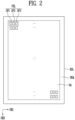
- FIG. 2 illustrates a display device in accordance with an embodiment of the present disclosure, and is a schematic plan view illustrating a display device using the light emitting element illustrated in FIG. 1 as a light emitting source.
- FIG. 2 schematically illustrates the structure of the display device, focused on a display area DA on which an image is displayed.
- at least one driving circuit e.g., a scan driver and a data driver
- a plurality of signal lines may be further provided in the display device.
- the display device in accordance with the embodiment of the present disclosure may include a base layer BSL, a plurality of pixels PXL provided on the base layer BSL and each including at least one light emitting element LD, a driver (not illustrated) provided on the base layer BSL and configured to drive the pixels PXL, and a line component (not illustrated) provided to couple the pixels PXL with the driver.
- the display device may be classified into a passive-matrix type display device and an active-matrix type display device according to a method of driving the light emitting element LD.
- each of the pixels PXL may include a driving transistor configured to control the amount of current to be supplied to the light emitting element LD, and a switching transistor configured to transmit data signals to the driving transistor.
- passive-matrix type display devices capable of selectively turning on each pixel PXL taking into account the resolution, the contrast, and the working speed have been mainstreamed.
- the present disclosure is not limited thereto.
- passive-matrix type display devices in which pixels PXL may be turned on by groups may also employ components (e.g., first and second electrodes) for driving the light emitting element LD.
- the base layer BSL may be a substrate of the display device, and include a display area DA and a non-display area NDA.
- the display area DA may be an area in which the pixels PXL for displaying an image are provided.
- the non-display area NDA may be an area in which the driver for driving the pixels PXL and some of the line component for coupling the pixels PXL to the driver are provided.
- the present disclosure is not limited thereto, and the locations thereof may be changed.
- the display area DA may have various shapes.
- the display area DA may be provided in various forms such as a closed polygon including sides formed of linear lines, a circle, an ellipse or the like including a side formed of a curved line, and a semicircle, a semi-ellipse or the like including sides formed of a linear line and a curved line.
- the non-display area NDA may be provided on at least one side of the display area DA. Although in the drawing there is illustrated a structure where the non-display area NDA encloses the display area DA, the present disclosure is not limited thereto.
- the base layer BSL may be a rigid substrate or a flexible substrate, and the present disclosure is not limited thereto.
- the base layer BSL may be a rigid substrate made of glass or reinforced glass, or a flexible substrate formed of a thin film made of plastic or metal.
- the base layer BSL may be a transparent substrate, but it is not limited thereto.
- the base layer BSL may be a translucent substrate, an opaque substrate, or a reflective substrate.
- the pixels PXL may be provided in the display area DA on the base layer BSL.
- Each of the pixels PXL refers to a smallest unit for displaying an image, and a plurality of pixels may be provided.
- Each of the pixels PXL may include a light emitting element LD configured to be driven in response to a scan signal and a data signal.
- the light emitting element LD may have a small size corresponding to the nanometer scale or the micrometer scale, and be coupled in parallel to light emitting elements LD disposed adjacent thereto.
- the light emitting element LD may form a light source of the corresponding pixel PXL.
- each of the pixels PXL may include a plurality of sub-pixels SP1, SP2, and SP3.
- each pixel PXL may include a first sub-pixel SP1, a second sub-pixel SP2, and a third sub-pixel SP3 which are configured to emit different colors of light.
- the first sub-pixel SP1 may be a red sub-pixel configured to emit red light
- the second sub-pixel SP2 may be a green sub-pixel configured to emit green light
- the third sub-pixel SP3 may be a blue sub-pixel configured to emit blue light.
- the color, type, and/or number of sub-pixels that form each pixel PXL are not limited to the foregoing examples.
- FIG. 2 illustrates that the pixels PXL are disposed in the display area DA in the form of a matrix in a first direction DR1 and a second direction DR2 different from the first direction DR1
- the disposition of the pixels PXL may be changed in various ways without being limited to the foregoing example.
- disposition of the plurality of sub-pixels of each of the pixels PXL may also be changed in various ways.
- the driver may provide a driving signal to each pixel PXL through the line component and thus control the operation of the pixel PXL.
- the line component is omitted for the convenience sake of explanation.
- the driver may include a scan driver configured to provide scan signals to the pixels PXL through scan lines, an emission driver configured to provide emission control signals to the pixels PXL through emission control lines, a data driver configured to provide data signals to the pixels PXL through data lines, and a timing controller.
- the timing controller may control the scan driver, the emission driver, and the data driver.
- FIGS. 3a to 3d are circuit diagrams illustrating examples of a unit light emitting area of the display device of FIG. 2 in accordance with various embodiments.
- each of the first to third sub-pixels may be configured of an active pixel.
- the type, the configuration, and/or the driving method of each of the first to third sub-pixels is not particularly limited.
- each of the first to third sub-pixels may be configured of a pixel of a passive or active display device which can have various known structures.
- the first to third sub-pixels may have substantially the same structure or similar structures.
- the first sub-pixel of the first to third sub-pixels will be described as a representative example.
- the first sub-pixel SP1 may include an emission area EMA configured to generate light having a luminance corresponding to a data signal, and a peripheral area disposed around the emission area EMA.
- the pixel driving circuit 144 for driving the emission area EMA may be disposed in the peripheral area.
- the pixel driving circuit 144 and the emission area EMA are illustrated as being separated from each other, a portion of the pixel driving circuit 144 may be disposed in the emission area EMA.
- the emission area EMA may include a plurality of light emitting elements LD coupled in parallel to each other between a first driving power supply VDD and a second driving power supply VSS.
- the first driving power supply VDD and the second driving power supply VSS may have different potentials.
- the first driving power supply VDD may be set as a high-potential power supply
- the second driving power supply VSS may be set as a low-potential power supply.
- a difference in potential between the first and second driving power supplies VDD and VSS may be set to a threshold voltage of the light emitting elements LD or more during an emission period of the first sub-pixel SP1.
- a first electrode (e.g., an anode electrode) of each of the light emitting elements LD may be coupled to the first driving power supply VDD via the pixel driving circuit 144.
- a second electrode (e.g., a cathode electrode) of each of the light emitting elements LD may be coupled to the second driving power supply VSS.
- Each of the light emitting elements LD may emit light at a luminance corresponding to driving current that is controlled by the pixel driving circuit 144.
- FIGS. 3a to 3d illustrate that the light emitting elements LD are coupled in parallel to each other in the same direction (e.g., a forward direction) between the first and second driving power supplies VDD and VSS, the present disclosure is not limited thereto.
- some of the light emitting elements LD may be coupled to each other in the forward direction between the first and second driving power supplies VDD and VSS, and the other light emitting elements LD may be coupled to each other in the reverse direction.
- One of the first and second driving power supplies VDD and VSS may be supplied in the form of an AC voltage.
- the light emitting elements LD may alternately emit light by the same connection direction groups.
- the first sub-pixel SP1 may include only a single light emitting element LD.
- the pixel driving circuit 144 may include first and second transistors T1 and T2, and a storage capacitor Cst.
- the structure of the pixel driving circuit 144 is not limited to that of the embodiment illustrated in FIG. 3a .
- a first electrode of the first transistor (T1; switching transistor) is coupled to a data line Dj, and a second electrode thereof is coupled to a first node N1.
- the first electrode and the second electrode of the first transistor T1 may be different electrodes. If the first electrode is a source electrode, the second electrode is a drain electrode.
- a gate electrode of the first transistor T1 is coupled to the scan line Si.
- the first transistor T1 When a scan signal having a voltage (e.g., a low-level voltage) capable of turning on the first transistor T1 is supplied from the scan line Si, the first transistor T1 is turned on to electrically couple the data line Dj with the first node N1.
- a data signal of a corresponding frame is supplied to the data line Dj, whereby the data signal is transmitted to the first node N1.
- the data signal transmitted to the first node N1 may be charged to the storage capacitor Cst.
- a first electrode of the second transistor (T2; driving transistor) is coupled to the first driving power supply VDD, and a second electrode of the second transistor (T2; driving transistor) is electrically coupled to the first electrode of each of the light emitting elements LD.
- a gate electrode of the second transistor T2 is coupled to the first node N1. As such, the second transistor T2 may control the amount of driving current to be supplied to the light emitting elements LD in response to the voltage of the first node N1.
- One electrode of the storage capacitor Cst is coupled to the first driving power supply VDD, and the other electrode thereof is coupled to the first node N1.
- the storage capacitor Cst is charged with a voltage corresponding to a data signal supplied to the first node N1, and maintains the charged voltage until a data signal of a subsequent frame is supplied.
- FIG. 3a illustrates the pixel driving circuit 144 having a relatively simple structure including the first transistor T1 configured to transmit the data signal to the first sub-pixel SP1, the storage capacitor Cst configured to store the data signal, and the second transistor T2 configured to supply driving current corresponding to the data signal to the light emitting elements LD.
- the present disclosure is not limited thereto, and the structure of the pixel driving circuit 144 may be changed in various ways.
- the pixel driving circuit 144 may further include at least one transistor element such as a transistor element configured to compensate for the threshold voltage of the second transistor T2, a transistor element configured to initialize the first node N1, and/or a transistor element configured to control an emission time of the light emitting elements LD, or other circuit elements such as a boosting capacitor for boosting the voltage of the first node N1.
- FIG. 3a illustrates that the transistors, e.g., the first and second transistors T1 and T2, included in the pixel driving circuit 144 are formed of P-type transistors, the type of the transistor is not limited thereto.
- the first and second transistors T1 and T2 included in the pixel driving circuit 144 may be an N-type transistor.
- the pixel driving circuit 144 may further include a third transistor T3 as well as including the first and second transistors T1 and T2.
- the third transistor T3 may be coupled between a j-th data line Dj and the anode electrode of each of the light emitting elements LD.
- the gate electrode of the third transistor T3 may be coupled to the control line CLi so that the third transistor T3 may be turned on when a control signal is supplied to the control line CLi, and be turned off in other cases.
- FIG. 3b illustrates that all of the first to third transistors T1 to T3 are formed of P-type transistors, but the present disclosure is not limited thereto.
- at least one of the first to third transistors T1 to T3 included in the pixel driving circuit 144 may be formed of an N-type transistor, or all of the first to third transistors T1 to T3 may be N-type transistors.
- the first and second transistors T1 and T2 may be N-type transistors.
- the configuration and operation of the pixel driving circuit 144 illustrated in FIG. 3c other than a change in connection positions of some components due to a change in the type of transistor, are similar to those of the pixel driving circuit 144 of FIG. 3a . Therefore, detailed descriptions pertaining to this will be omitted.
- the pixel driving circuit 144 may be coupled to the scan line Si and the data line Dj of the first sub-pixel SP1.
- the pixel driving circuit 144 of the first sub-pixel SP1 may be coupled to an i-th scan line Si and a j-th data line Dj of the display area DA.
- the pixel driving circuit 144 may also be coupled to at least one other scan line.
- the first sub-pixel SP1 disposed on the i-th row of the display area DA may be further coupled to an i-1-th scan line Si-1 and/or an i+1-th scan line Si+1.
- the pixel driving circuit 144 may be coupled not only to the first and second driving power supplies VDD and VSS but also to a third power supply.
- the pixel driving circuit 144 may also be coupled to an initialization power supply Vint.
- the pixel driving circuit 144 may include first to seventh transistors T1 to T7, and a storage capacitor Cst.
- One electrode of the first transistor (T1; driving transistor), e.g., a source electrode, may be coupled to the first driving power supply VDD via the fifth transistor T5, and the other electrode thereof, e.g., a drain electrode, may be coupled to one end of light emitting elements LD via the sixth transistor T6.
- a gate electrode of the first transistor T1 may be coupled to a first node N1.
- the first transistor T1 may control driving current flowing between the first driving power supply VDD and the second driving power supply VSS via the light emitting elements LD in response to the voltage of the first node N1.
- the second transistor may be coupled between the j-th data line Dj coupled to the first sub-pixel SP1 and the source electrode of the first transistor T1.
- a gate electrode of the second transistor T2 is coupled to the i-th scan line Si coupled to the first sub-pixel SP1.
- a scan signal having a gate-on voltage e.g., a low-level voltage
- the second transistor T2 is turned on to electrically couple the j-th data line Dj to the source electrode of the first transistor T1.
- a data signal supplied from the j-th data line Dj may be transmitted to the first transistor T1.
- the third transistor T3 is coupled between the drain electrode of the first transistor T1 and the first node N1.
- a gate electrode of the third transistor T3 is coupled to the i-th scan line Si.
- the third transistor T3 is turned on to electrically couple the drain electrode of the first transistor T1 to the first node N1. Therefore, when the third transistor T3 is turned on, the first transistor T1 may be connected in the form of a diode.
- the fourth transistor T4 may be coupled between the first node N1 and the initialization power supply Vint.
- a gate electrode of the fourth transistor T4 is coupled to a previous scan line, e.g., an i-1-th scan line Si-1.
- the fourth transistor T4 is turned on so that the voltage of the initialization power supply Vint may be transmitted to the first node N1.
- the initialization power supply Vint may have a voltage equal to or less than the minimum voltage of the data signal.
- the fifth transistor T5 is coupled between the first driving power supply VDD and the first transistor T1.
- a gate electrode of the fifth transistor T5 is coupled to a corresponding emission control line, e.g., an i-th emission control line Ei.
- the fifth transistor T5 may be turned off when an emission control signal having a gate-off voltage is supplied to the i-th emission control line Ei, and may be turned on in other cases.
- the sixth transistor T6 is coupled between the first transistor T1 and one end of the light emitting elements LD.
- a gate electrode of the sixth transistor T6 may be coupled to the i-th emission control line Ei.
- the sixth transistor T6 may be turned off when an emission control signal having a gate-off voltage is supplied to the i-th emission control line Ei, and may be turned on in other cases.
- the seventh transistor T7 is coupled between the one end of the light emitting elements LD and the initialization power supply Vint.
- a gate electrode of the seventh transistor T7 is coupled to any one of scan lines of a subsequent stage, e.g., to the i+1-th scan line Si+1.
- the seventh transistor T7 may be turned on so that the voltage of the initialization power supply Vint may be supplied to the first end of the light emitting elements LD.
- the storage capacitor Cst is coupled between the first driving power supply VDD and the first node N1.
- the storage capacitor Cst may store a voltage corresponding both to the data signal applied to the first node N1 during each frame period and to the threshold voltage of the first transistor T1.
- FIG. 3d illustrates that all of the first to seventh transistors T1 to T7 are formed of P-type transistors, but the present disclosure is not limited thereto.
- at least one of the first to seventh transistors T1 to T7 included in the pixel driving circuit 144 may be formed of an N-type transistor, or all of the first to seventh transistors T1 to T7 may be N-type transistors.
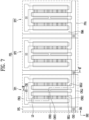
- FIG. 4 is a plan view schematically illustrating first to third sub-pixels included in one of the pixels illustrated in FIG. 2 in accordance with an embodiment of the present disclosure.
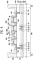
- FIG. 5 is a sectional view taken along line I-I' of FIG. 4 .
- FIG. 4 illustrates that a plurality of light emitting elements LD provided in each sub-pixel are horizontally aligned
- the arrangement of the light emitting elements LD is not limited thereto.
- at least some of the light emitting elements LD may be aligned in a direction intersecting with the horizontal direction.
- illustration of transistors coupled to the light emitting elements LD, and signal lines coupled to the transistors has been omitted in FIGS. 4 and 5 .
- FIGS. 4 and 5 illustrate a simplified structure of the one pixel PXL, e.g., showing that each electrode has only a single electrode layer, the present disclosure is not limited thereto.
- the display device in accordance with an embodiment of the present disclosure may include a base layer BSL on which a plurality of pixels PXL are provided.
- Each of the pixels PXL may include a first sub-pixel SP1, a second sub-pixel SP2, and a third sub-pixel SP3 which are provided on the base layer BSL.
- the first sub-pixel SP1 may be a red sub-pixel configured to emit red light
- the second sub-pixel SP2 may be a green sub-pixel configured to emit green light
- the third sub-pixel SP3 may be a blue sub-pixel configured to emit blue light.
- the color, type, and/or number of sub-pixels that form each pixel PXL are not limited to the foregoing examples.
- Each of the first to third sub-pixels SP1 to SP3 may include an emission area EMA configured to emit light, and a peripheral area PPA disposed around a perimeter of the emission area EMA.
- Each of the first to third sub-pixels SP1 to SP3 may include a base layer BSL, a pixel circuit layer PCL, and a display element layer DPL.
- the pixel circuit layer PCL may include a buffer layer BFL disposed on the base layer BSL, first and second transistors T1 and T2 disposed on the buffer layer BFL, and a driving voltage line DVL. Furthermore, the pixel circuit layer PCL of each of the first to third sub-pixels SP1 to SP3 may further include a passivation layer PSV which is disposed on the first and second transistors T1 and T2 and the driving voltage line DVL.
- the base layer BSL may be a rigid or flexible substrate, and the material or properties thereof are not particularly limited.
- the base layer BSL may be a rigid substrate made of glass or reinforced glass, or a flexible substrate formed of a thin film made of plastic or metal.
- the base layer BSL may be a transparent substrate, but the present disclosure is not limited thereto, and the base layer BSL may be a translucent substrate, an opaque substrate, or a reflective substrate.
- the base layer BSL may have a multilayer structure.
- the buffer layer BFL may prevent impurities from being diffused into the first and second transistors T1 and T2.
- the buffer layer BFL may be omitted depending on the material of the substrate SUB or processing conditions.
- the first transistor T1 may be electrically coupled with some of the light emitting elements LD provided on the display element layer DPL of the corresponding sub-pixel.
- the first transistor T1 may be a driving transistor configured to drive the light emitting elements LD.
- the second transistor T2 may be a switching transistor configured to switch the first transistor T1.
- Each of the first and second transistors T1 and T2 may include a semiconductor layer SCL, a gate electrode GE, a source electrode SE, and a drain electrode DE.
- the semiconductor layer SCL may be disposed on the buffer layer BFL.
- the semiconductor layer SCL may include a source area which comes into contact with the source electrode SE, and a drain area which comes into contact with the drain electrode DE.
- An area between the source area and the drain area may be a channel area.
- the semiconductor layer SCL may be a semiconductor pattern formed of polysilicon, amorphous silicon, an oxide semiconductor, etc.
- the channel area may be an intrinsic semiconductor, which is an undoped semiconductor pattern.
- Each of the source area and the drain area may be a semiconductor pattern doped with an impurity.
- the gate electrode GE may be provided on the semiconductor layer SCL with the gate insulating layer GI interposed therebetween.
- the source electrode SE and the drain electrode DE may respectively come into contact with the source area and the drain area of the semiconductor layer SCL through corresponding contact holes which pass through an interlayer insulating layer ILD and the gate insulating layer GI.
- first and second transistors T1 and T2 are LTPS thin-film transistors, the first and second transistors T1 and T2 are not limited thereto.
- the driving voltage line DVL is illustrated as being disposed on the interlayer insulating layer ILD, the location of the driving voltage line DVL is not limited thereto.
- the driving voltage line DVL may be disposed on any one of the insulating layers included in the pixel circuit layer PCL.
- the second driving power supply (refer to VSS of FIG. 3a ) may be applied to the driving voltage line DVL.
- the passivation layer PSV may include a first contact hole CH1 which exposes a portion of the drain electrode DE of the first transistor T1, and a second contact hole CH2 which exposes a portion of the driving voltage line DVL.
- the display element layer DPL may be disposed on the pixel circuit layer PCL.
- the display element layer DPL may include a wall PW, a bank BNK, first and second electrodes REL1 and REL2, first and second connection lines CNL1 and CNL2, a plurality of light emitting elements LD, first and second contact electrodes CNE1 and CNE2, etc.
- the wall PW may be provided on the passivation layer PSV in the emission area EMA of each of the first to third sub-pixels SP1 to SP3.
- a bank BNK formed of the same material as that of the wall PW may be formed and/or provided between adjacent sub-pixels to define the emission area EMA of each sub-pixel.
- the adjacent walls PW may be disposed on the passivation layer PSV and spaced apart from each other by a length L of one light emitting element LD or more.
- the light emitting elements LD may be disposed between the adjacent walls PW in the emission area EMA.
- the wall PW may include a curved surface having a cross-sectional shape such as a semicircle, or a semiellipse which is reduced in width upward from one surface of the passivation layer PSV.
- the wall PW is illustrated as having a trapezoidal cross-section.
- the shape of each of the walls PW is not limited to the foregoing examples, and may be changed in various ways within a range in which the efficiency of light emitted from each of the light emitting elements LD can be enhanced.
- the bank BNK may be further disposed on the passivation layer PSV.
- the bank BNK may be disposed in the peripheral area PPA between the adjacent sub-pixels SP1 to SP3 and define the emission area EMA of each of the sub-pixels SP1 to SP3.
- the bank BNK may prevent light emitted from the sub-pixels SP1 to SP3 from traveling to the adjacent sub-pixels SP1 to SP3.
- the wall PW and the bank BNK may be formed of the same material on the same layer.
- the wall PW and the bank BNK may be formed of organic insulating material including organic material, the present disclosure is not limited thereto.
- the first connection line CNL1 may be electrically coupled with the pixel circuit layer PCL through the first contact hole CH1 formed in the passivation layer PSV.
- the first connection line CNL1 may be connected with a portion of the drain electrode DE of the first transistor T1 of the pixel circuit layer PCL.
- the first contact hole CH1 is illustrated as being formed in the peripheral area PPA, the first contact hole CH1 may be formed in the emission area EMA.
- the first connection line CNL1 may extend from each of the first to third sub-pixels SP1 to SP3 in the first direction DR1. To independently drive each of the first to third sub-pixels SP1 to SP3, one first connection line CNL1 may be provided in each sub-pixel.
- the second connection line CNL2 may also be electrically coupled with the pixel circuit layer PCL through the second contact hole CH2 formed in the passivation layer PSV.
- the second connection line CNL2 may be connected with a portion of the driving voltage line DVL of the pixel circuit layer PCL.
- the second connection line CNL2 may extend in a direction parallel to a direction in which the first connection line CNL1 extends.
- the second connection line CNL2 may be provided in common to the first to third sub-pixels SP1 to SP3. Therefore, the first to third sub-pixels SP1 to SP3 may be coupled in common to the second connection line CNL2.
- Each of the first and second electrodes REL1 and REL2 may be provided in the emission area EMA of each of the first to third sub-pixels SP1 to SP3 and extend in the second direction DR2 intersecting with the first direction DR1.
- the first and second electrodes REL1 and REL2 may be provided on the same plane and spaced apart from each other by a predetermined distance.
- first and second electrodes REL1 and REL2 are disposed in each of the sub-pixels SP1 to SP3
- one or more first and second electrodes REL1 and REL2 may be disposed in each of the sub-pixels SP1 to SP3.
- the first and second electrodes REL1 and REL2 may be alternately disposed.
- the first electrode REL1 may be coupled to the first connection line CNL1.
- the first electrode REL1 may be integrally coupled with the first connection line CNL1.
- the first electrode REL1 diverges from the first connection line CNL1 in the second direction DR2.
- the first electrode REL1 has two first electrode patterns, the number of first electrodes REL1 and the number of first electrode patterns are not limited thereto.
- the first connection line CNL1 may be regarded as one area of the first electrode RELL.
- the present disclosure is not limited thereto.
- the first electrode REL1 and the first connection line CNL1 may be individually formed and electrically coupled to each other through a contact hole, via hole, or the like, which is not illustrated.
- the first electrode REL1 may be disposed adjacent to one end of the opposite ends EP1 and EP2 of each of the light emitting elements LD.
- the first electrode REL1 is disposed adjacent to the first end EP1 of the light emitting elements LD, and the first electrode REL1 is electrically coupled to the first end EP1 of the light emitting elements LD through the first contact electrode CNE1. Therefore, a signal of the first transistor T1 that is applied to the first electrode REL1 may be transmitted to each of the light emitting elements LD through the first contact electrode CNE1.
- the second electrode REL2 may be coupled to the second connection line CNL2.
- the second electrode REL2 may be integrally coupled with the second connection line CNL2.
- the number of second electrodes REL2 and the number of first electrode patterns are not limited thereto.
- the second connection line CNL2 may be regarded as one area of the second electrode REL2.
- the present disclosure is not limited thereto.
- the second electrode REL2 and the second connection line CNL2 may be individually formed and electrically coupled to each other through a contact hole, via hole, or the like, which is not illustrated.
- the second electrode REL2 may be disposed adjacent to the other end of the opposite ends EP1 and EP2 of each of the light emitting elements LD.
- the second electrode REL2 is electrically coupled to the second end EP2 of the light emitting elements LD through the second contact electrode CNE2.
- the voltage of the second driving power supply VSS applied to the second electrode REL2 may be transmitted to each of the light emitting elements LD.
- Each of the first and second electrodes REL1 and REL2 may function as an alignment electrode for aligning the light emitting elements LD in the emission area EMA of each of the first to third sub-pixels SP1 to SP3.
- a first alignment voltage may be applied to the first electrode REL1 through the first connection line CNL1
- a second alignment voltage may be applied to the second electrode REL2 through the second connection line CNL2.
- the first alignment voltage and the second alignment voltage may have different voltage levels.
- predetermined alignment voltages having different voltage levels are respectively applied to the first electrode REL1 and the second electrode REL2, an electric field may be formed between the first electrode REL1 and the second electrode REL2.
- the light emitting elements LD may be aligned between the first electrode REL1 and the second electrode REL2.
- the second electrodes REL2 and the first electrodes REL1 may be alternately disposed.
- the second electrode REL2 is disposed between the first electrodes REL1.
- each of the first and second electrodes REL1 and REL2 may function as a driving electrode for driving the light emitting elements LD.
- the first and second electrodes REL1 and REL2 provided on the wall PW may be made of material having a predetermined reflectivity to allow light emitted from the opposite ends EP1 and EP2 of each of the light emitting elements LD to travel in a direction (e.g., in a frontal direction) in which an image of the display device is displayed.
- the first and second electrodes REL1 and REL2 may function as reflectors for enhancing the efficiency of light emitted from the light emitting elements LD.
- first and second electrodes REL1 and REL2, and the first and second connection lines CNL1 and CNL2 may be formed of conductive material having a predetermined reflectivity.
- Metal for example, Ag, Mg, Al, Pt, Pd, Au, Ni, Nd, Ir, Cr, Ti, and an alloy thereof may be used as the conductive material.
- the materials of the first and second electrodes REL1 and REL2, and the first and second connection lines CNL1 and CNL2 are not limited to the foregoing materials.
- each of the first and second electrodes REL1 and REL2 and the first and second connection lines CNL1 and CNL2 may have a multilayer structure formed by stacking two or more materials among metals, alloys, conductive oxides, and conductive polymers.
- first and second electrodes REL1 and REL2 may be an anode electrode, and the other may be a cathode electrode.
- first electrode REL1 may be an anode electrode
- second electrode REL2 may be a cathode electrode.
- At least one first connection pattern CNP1 may be disposed in the emission area EMA.
- the at least one first connection pattern CNP1 may couple two first electrode patterns spaced apart from each other.
- at least one first connection pattern CNP1 may couple the first electrode patterns of the first electrode REL1 or the first electrode patterns of the second electrode REL2.
- FIG. 1 there is illustrated the case where at least one first connection pattern CNP1 couples the first electrode patterns of the second electrode REL2.
- the first connection pattern CNP1 may be spaced apart from the second connection line CNL2 and be disposed in the emission area EMA of each of the sub-pixels SP1 to SP3.
- the first connection pattern CNP1 may be integrally formed with the second electrode REL2.
- the first connection pattern CNP1 may function to minimize the non-emission area of the sub-pixel.
- a portion of the second electrode REL2 that is coupled to the defective light emitting element may be disconnected (open).
- the other light emitting elements LD are coupled with the second electrode REL2 by the first connection pattern CNP1 and thus may be normally operated.
- Each of the light emitting elements LD may be formed of a light emitting diode which is made of material having an inorganic crystal structure and has a subminiature size, e.g., corresponding to the nanoscale or the microscale.
- the present disclosure is not limited thereto.
- the number of light emitting elements LD provided in each sub-pixel may be changed in various ways.
- Each of the light emitting elements LD may include a stacked emission pattern formed by successively stacking a first conductive semiconductor layer 11, an active layer 12, and a second conductive semiconductor layer 13 in the longitudinal direction (L) of each light emitting element LD. Furthermore, each of the light emitting elements LD may further include an insulating film 14 which encloses an outer circumferential surface of the stacked emission pattern. In an embodiment of the present disclosure, each of the light emitting elements LD may have a cylindrical shape.
- each light emitting element LD may have a first end EP1 corresponding to any one of a lower portion of the cylinder and an upper portion of the cylinder, and a second end EP2 corresponding to the other of the lower portion of the cylinder and the upper portion of the cylinder.
- Any one of the first conductive semiconductor layer 11 and the second conductive semiconductor layer 13 may be disposed on the first end EP1 of each light emitting element LD, and the other of the first conductive semiconductor layer 11 and the second conductive semiconductor layer 13 may be disposed on the second end EP2 thereof.
- the light emitting elements LD may be aligned between the first electrode REL1 and the second electrode REL2.
- a second insulating layer INS2 may be provided on the light emitting elements LD to cover a portion of an upper surface of each of the light emitting elements LD.
- a first insulating layer INS1 may be provided between each of the light emitting elements LD and the passivation layer PSV.
- the first insulating layer INS1 may be filled into space between the passivation layer PSV and each of the light emitting elements LD to stably support the light emitting elements LD and prevent the light emitting elements LD from being removed from the passivation layer PSV.
- the first insulating layer INS1 may be formed of an inorganic insulating layer including inorganic material, or an organic insulating layer including organic material. Although in an embodiment of the present disclosure the first insulating layer INS1 may be formed of inorganic insulating layer having an advantage in protecting the light emitting elements LD from the pixel circuit layer PCL, the present disclosure is not limited thereto. In an embodiment, the first insulating layer INS1 may be formed of an organic insulating layer that has an advantage in planarization of support surfaces of the light emitting elements LD.
- the second insulating layer INS2 may be disposed on the light emitting elements LD.
- the second insulating layer INS2 may be an organic insulating layer including organic material.
- the second insulating layer INS2 may be provided on a portion of the upper surface of each of the light emitting elements LD such that the opposite ends EP1 and EP2 of each of the light emitting elements LD may be exposed to the outside.
- the first and second contact electrodes CNE1 and CNE2 may be coupled to the exposed opposite ends EP1 and EP2 of the light emitting elements LD.
- the first and second contact electrodes CNE1 and CNE2 may be provided on the same plane, and may be spaced apart from each other by a predetermined distance on the second insulating layer INS2 and thus electrically and/or physically separated from each other.
- the first contact electrode CNE1 and the second contact electrode CNE2 may be provided on the same layer and formed through the same fabricating process.
- the first and second contact electrodes CNE1 and CNE2 may be provided on different layers.
- the first and second contact electrodes CNE1 and CNE2 may be coupled with the first and second electrodes REL1 and REL2 exposed from the first insulating layer INS1.
- the first and second contact electrodes CNE1 and CNE2 along with the first and second electrodes REL1 and REL2 may be disposed on the wall PW.
- the first and second contact electrodes CNE1 and CNE2 may extend in a direction in which the first and second electrodes REL1 and REL2 extend, and may respectively overlap with the first and second electrodes REL1 and REL2 on the corresponding walls PW.
- the first contact electrode CNE1 may include second electrode patterns respectively coupled with the first electrode patterns of the first electrode RELL.
- the second contact electrode CNE2 may also include second electrode patterns respectively coupled with the first electrode patterns of the second electrode REL2.
- the first and second contact electrodes CNE1 and CNE2 may be formed of transparent conductive material to allow light emitted from the light emitting elements LD to travel in the frontal direction of the display device by the first and second electrodes REL1 and REL2.
- a third insulating layer INS3 for covering the first and second contact electrodes CNE1 and CNE2 may be provided on the first and second contact electrodes CNE1 and CNE2.
- the third insulating layer INS3 may prevent the first and second contact electrodes CNE1 and CNE2 from being exposed to the outside, thus preventing the first and second contact electrodes CNE1 and CNE2 from being corroded.
- the third insulating layer INS3 may be formed of an inorganic insulating layer including inorganic material, or an organic insulating layer including organic material.
- the third insulating layer INS3 may have a single layer structure as shown in the drawing, the present disclosure is not limited thereto.
- the third insulating layer INS3 may have a multilayer structure.
- the third insulating layer INS3 may have a structure formed by alternately stacking a plurality of inorganic insulating layers and a plurality of organic insulating layers.
- the third insulating layer INS3 may have a structure formed by sequentially stacking a first inorganic insulating layer, an organic insulating layer, and a second inorganic insulating layer.
- the opposite ends EP1 and EP2 of the light emitting elements LD may be respectively coupled to the first electrode REL1 and the second electrode REL2 through the first and second contact electrodes CNE1 and CNE2 so that predetermined voltages can be respectively applied to the opposite ends EP1 and EP2, and each of the light emitting elements LD can emit light by coupling of electron-hole pairs in the active layer 12 of the light emitting element LD.
- the active layer 12 may emit light having a wavelength range from 400 nm to 900 nm.
- the wavelength range of light emitted from the active layer 12 is not limited thereto, and may be changed in various ways.
- the first electrode patterns of the second electrode REL2 may be coupled to each other through at least one first connection pattern CNP1, so that even when some light emitting elements LD are defective, the number of light emitting elements LD that do not emit light can be minimized.
- the first connection pattern CNP1 may be formed in various shapes and couple the first electrode patterns of the second electrode REL2 to each other.
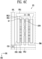
- FIGS. 6a to 6c are plan views of the sub-pixel of FIG. 4 showing various shapes of the first connection pattern.
- the first electrode patterns of the second electrode REL2 may be coupled to each other through a plurality of first connection patterns CNP1.
- the plurality of first connection patterns CNP1 may be disposed in a direction perpendicular to a direction in which the second electrodes REL2 extend, as illustrated in FIGS. 6a and 6b , or may be disposed in a diagonal direction, as illustrated in FIG. 6c .
- the second electrode patterns of one of the first contact electrode CNE1 and the second contact electrode CNE2 may be coupled through at least one second connection pattern CNP2.
- FIG. 7 is a plan view schematically illustrating first to third sub-pixels included in one of the pixels illustrated in FIG. 2 in accordance with an another embodiment of the present disclosure.
- FIG. 8 is a sectional view taken along line II-II' of FIG. 7 .
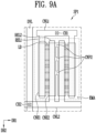
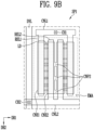
- FIGS. 9a to 9d are plan views of a sub-pixel of FIG. 7 showing various shapes of a second connection pattern.
- the second electrode patterns of the second contact electrode CNE2 may be coupled through the second connection pattern CNP2.
- the second electrode patterns of the second contact electrode CNE2 and the second connection pattern CNP2 may be formed integrally with each other.
- a plurality of second connection patterns CNP2 may be provided.
- the first electrode patterns of one of the first electrode REL1 and the second electrode REL2 may be coupled through at least one first connection pattern CNP1.
- the second electrode patterns of one of the first contact electrode CNE1 and the second contact electrode CNE2 may be coupled through at least one second connection pattern CNP2.
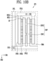
- FIG. 10a is a plan view schematically illustrating first to third sub-pixels included in one of the pixels illustrated in FIG. 2 in accordance with an another embodiment of the present disclosure.
- FIGS. 10b and 10c are plan views of a sub-pixel of FIG. 10a in which first and second connection patterns are spaced apart from each other.
- the first electrode patterns of the second electrode REL2 may be coupled through the first connection pattern CNP1
- the second electrode patterns of the second contact electrode CNE2 may be coupled through the second connection pattern CNP2.
- the first connection pattern CNP1 and the second connection pattern CNP2 may completely overlap with each other, or at least partially overlap with each other.
- the first connection pattern CNP1 and the second connection pattern CNP2 may be spaced apart from each other rather than overlapping with each other.
- the number of first connection patterns CNP1 and the number of second connection patterns CNP2 may differ from each other.
- At least one first connection pattern CNP1 may couple the first electrode patterns of the first electrode REL1.
- a sub-pixel may be repaired by cutting off a portion of the first electrode REL1.
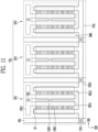
- FIG. 11 is a plan view schematically illustrating first to third sub-pixels included in one of the pixels illustrated in FIG. 2 in accordance with a modification of an embodiment of the present disclosure.
- FIGS. 12a and 12b are plan views of a sub-pixel of FIG. 11 showing various shapes of a connection pattern.
- the first connection pattern CNP1 disposed in the emission area EMA may couple the first electrode patterns of the first electrode REL1.
- the first connection pattern CNP1 may be integrally formed with the first electrode patterns of the first electrode REL1.
- the first electrodes REL1 may be disposed between the second electrodes REL2.
- a portion of the first electrode REL1 that is coupled with the defective light emitting element may be disconnected (open).
- the other portion of the first electrode REL1 may be coupled by the first connection pattern CNP1, so that the number of light emitting elements LD that do not emit may be minimized.
- the first contact electrode CNE1 may include the second electrode patterns, so that the second electrode patterns of the first contact electrode CNE1 can be integrated with the second connection pattern CNP2.
- the first electrode patterns of the first electrode REL1 may be coupled through the first connection pattern CNP1
- the second electrode patterns of the first contact electrode CNE1 may be coupled through the second connection pattern CNP2.
- first connection pattern CNP1 and the second connection pattern CNP2 may be spaced apart from each other not to overlap with each other.
- the number of first connection patterns CNP1 and the number of second connection patterns CNP2 may differ from each other.
- the display device when the sub-pixels SP1 to SP3 in which defective light emitting elements DLD are disposed are repaired, some of the first electrodes REL1 and the first contact electrodes CNE1 or the second electrodes REL2 and the second contact electrodes CNE2 that are coupled through at least one of the first and second connection patterns CNP1 and CNP2 may be opened, so that the number of light emitting elements LD that do not emit light may be minimized.
- the first connection pattern CNP1 directly couples the first electrode patterns of the first electrode REL1 or the second connection pattern CNP2 is formed integrally with the second electrode patterns of the first contact electrode CNE1 so that the first electrode patterns of the first electrode REL1 are indirectly coupled by the second connection patterns CNP2, peripherals of the first electrode REL1 that are coupled with defective light emitting elements DLD may be opened.
- FIG. 13a is a view illustrating a defect caused by a defective light emitting element in accordance with an embodiment of the present disclosure, and illustrates only a sub-pixel of a pixel illustrated in FIG. 2 .
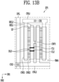
- FIG. 13b is a diagram illustrating a repair method of FIG. 13a .
- FIG. 13c is a diagram of FIG. 13b illustrating an emission area after a repair operation.
- the first electrode REL1 and the second electrode REL2 may be short-circuited by the defective light emitting elements DLD. In this case, signals cannot be transmitted through the first contact hole (CH1 of FIG. 4 ) to some light emitting elements LD disposed in parallel with the defective light emitting elements DLD.
- signals may not be transmitted through the first contact hole (CH1 of FIG. 4 ) to light emitting elements LD that are disposed closer to a distal end of the first electrode REL1 than are the defective light emitting elements DLD. Therefore, an area including the light emitting elements LD to which signals cannot be transmitted through the first contact hole (CH1 of FIG. 4 ) may be a non-emission area NEMA.
- a portion of the first electrode pattern coupled to the first connection pattern CNP1 among one ends of the defective light emitting elements DLD may be disconnected (open), so that defects of the sub-pixel attributable to the defective light emitting elements DLD can be repaired.
- the location of the defective light emitting elements DLD is checked, and then a portion of the second electrode REL2 is cut off through a process such as a laser cutting process.
- a first cutting line CL1 is formed on the second contact electrode CNE2 that couples the second electrode REL2 with one end of the opposite ends of each defective light emitting element DLD.
- a second cutting line CL2 is formed on the second contact electrode CNE2 at a position spaced apart from the first cutting line CL1.
- the junction between the defective light emitting elements DLD and the second contact electrode CNE2 is disposed between the first cutting line CL1 and the second cutting line CL2.
- the location of the defective light emitting elements DLD is checked, and then a portion of the first electrode REL1 may be cut off through a process such as a laser cutting process.
- the first cutting line CL1 is formed on the first contact electrode CNE1 that couples the first electrode REL1 with one end of the opposite ends of each defective light emitting element DLD.
- the second cutting line CL2 is formed on the first contact electrode CNE1 at a position spaced apart from the first cutting line CL1.
- the junction between the defective light emitting elements DLD and the first contact electrode CNE1 is disposed between the first cutting line CL1 and the second cutting line CL2.
- the first electrode REL1 and the first contact electrode CNE1 or the second electrode REL2 and the second contact electrode CNE2 in an area coupled with the defective light emitting elements DLD may float. Therefore, signals of the pixel circuit layer cannot be transmitted to only the defective light emitting elements DLD, so that only an area where the defective light emitting elements DLD are disposed is a non-emission area NEMA, and the other light emitting elements LD may receive the signals of the pixel circuit layer through the connection pattern CNP and normally emit light. Consequently, the size of a non-emission area formed by a repair may be minimized.
Landscapes
- Engineering & Computer Science (AREA)
- Physics & Mathematics (AREA)
- Computer Hardware Design (AREA)
- General Physics & Mathematics (AREA)
- Theoretical Computer Science (AREA)
- Electroluminescent Light Sources (AREA)
- Devices For Indicating Variable Information By Combining Individual Elements (AREA)
Claims (14)
- Dispositif d'affichage comprenant :une couche de base (BSL) incluant une zone d'affichage (DA) et une zone de non-affichage (NDA) ; etune pluralité de pixels (PXL) fournis dans la zone d'affichage (DA) et comprenant chacun une pluralité de sous-pixels (SP1, SP2, SP3) incluant chacun une zone d'émission (EMA) configurée pour émettre de la lumière et une zone périphérique (PPA) fournie autour de la zone d'émission (EMA),dans lequel les sous-pixels (SP1, SP2, SP3) comprennent :au moins une première électrode (REL1) et au moins une deuxième électrode (REL2) s'étendant dans une direction et espacées l'une de l'autre ; etune pluralité d'éléments électroluminescents (LD) disposés entre la première électrode (REL1) et la deuxième électrode (REL2) et configurés pour émettre de la lumière,dans lequel au moins une de la première électrode (REL1) et de la deuxième électrode (REL2) comprend au moins deux premiers motifs d'électrode espacés l'un de l'autre, et les premiers motifs d'électrode sont couplés par au moins un premier motif de connexion (CNP1) disposé dans la zone d'émission (EMA),dans lequel :(i) il existe deux deuxièmes électrodes (REL2) qui sont adjacentes l'une à l'autre, et la première électrode (REL1) est disposée entre les deux deuxièmes électrodes (REL2) adjacentes l'une à l'autre, et
dans lequel la première électrode (REL1) inclut les au moins deux premiers motifs d'électrode ; ou(ii) il existe deux premières électrodes (REL1) qui sont adjacentes l'une à l'autre, et la deuxième électrode (REL2) est disposée entre les deux premières électrodes (REL1) adjacentes l'une à l'autre, etdans lequel la deuxième électrode (REL2) inclut les au moins deux premiers motifs d'électrode. - Dispositif d'affichage selon la revendication 1, dans lequel le premier motif de connexion (CNP1) est formé d'un seul tenant avec les premiers motifs d'électrode.
- Dispositif d'affichage selon la revendication 1 ou la revendication 2, comprenant :une première électrode de contact (CNE1) s'étendant le long de la première électrode (REL1) et configurée pour coupler la première électrode (REL1) à une extrémité d'extrémités opposées de l'élément électroluminescent (LD) ; etune deuxième électrode de contact (CNE2) s'étendant le long de la deuxième électrode (REL2) et configurée pour coupler la deuxième électrode (REL2) à une extrémité résiduelle des extrémités opposées de l'élément électroluminescent (LD),dans lequel au moins une de la première électrode de contact (CNE1) et de la deuxième électrode de contact (CNE2) comprend au moins deux deuxièmes motifs d'électrode espacés l'un de l'autre, et les deuxièmes motifs d'électrode sont couplés par au moins un deuxième motif de connexion (CNP2).
- Dispositif d'affichage selon la revendication 3, dans lequel le deuxième motif de connexion (CNP2) est formé d'un seul tenant avec une de la première électrode de contact (CNE1) et de la deuxième électrode de contact (CNE2).
- Dispositif d'affichage selon la revendication 4,dans lequel le deuxième motif de connexion (CNP2) est formé d'un seul tenant avec la première électrode de contact (CNE1), etdans lequel la première électrode (REL1) est disposée entre le deuxième motif de connexion (CNP2) et les éléments électroluminescents (LD).
- Dispositif d'affichage selon la revendication 4,dans lequel le deuxième motif de connexion (CNP2) est formé d'un seul tenant avec la deuxième électrode de contact (CNE2), etdans lequel la deuxième électrode (REL2) est disposée entre le deuxième motif de connexion (CNP2) et les éléments électroluminescents (LD).
- Dispositif d'affichage selon l'une quelconque des revendications 3 à 6, dans lequel :(i) le premier motif de connexion (CNP1) et au moins une partie du deuxième motif de connexion (CNP2) se chevauchent ; ou(ii) le premier motif de connexion (CNP1) et le deuxième motif d'électrode sont espacés l'un de l'autre.
- Dispositif d'affichage selon l'une quelconque des revendications 3 à 7, dans lequel un nombre de premiers motifs de connexion (CNP1) et un nombre de deuxièmes motifs de connexion (CNP2) diffèrent l'un de l'autre.
- Dispositif d'affichage comprenant :une couche de base (BSL) incluant une zone d'affichage (DA) et une zone de non-affichage (NDA) ; etune pluralité de pixels (PXL) fournis dans la zone d'affichage (DA) et comprenant chacun une pluralité de sous-pixels (SP1, SP2, SP3) incluant chacun une zone d'émission (EMA) configurée pour émettre de la lumière et une zone périphérique (PPA) fournie autour de la zone d'émission (EMA),dans lequel les sous-pixels (SP1, SP2, SP3) comprennent :au moins une première électrode (REL1) et au moins une deuxième électrode (REL2) s'étendant dans une direction et espacées l'une de l'autre ;une pluralité d'éléments électroluminescents (LD) disposés entre la première électrode (REL1) et la deuxième électrode (REL2) et configurés pour émettre de la lumière ;une première électrode de contact (CNE1) s'étendant le long de la première électrode (REL1) et configurée pour coupler la première électrode (REL1) à une extrémité d'extrémités opposées de l'élément électroluminescent (LD) ; etune deuxième électrode de contact (CNE2) s'étendant le long de la deuxième électrode (REL2) et configurée pour coupler la deuxième électrode (REL2) à une extrémité résiduelle des extrémités opposées de l'élément électroluminescent (LD),dans lequel au moins une de la première électrode (REL1) et de la deuxième électrode (REL2) comprend au moins deux premiers motifs d'électrode espacés l'un de l'autre, etcaractérisé en ce qu'au moins une de la première électrode de contact (CNE1) et de la deuxième électrode de contact (CNE2) comprend au moins deux deuxièmes motifs d'électrode espacés l'un de l'autre, et les deuxièmes motifs d'électrode sont couplés par au moins un motif de connexion (CNP2) disposé dans la zone d'émission (EMA).
- Dispositif d'affichage selon la revendication 9, dans lequel :(i) le motif de connexion (CNP1, CNP2) est formé d'un seul tenant avec la première électrode de contact (CNE1), et
dans lequel la première électrode (REL1) est disposée entre le motif de connexion (CNP2) et les éléments électroluminescents (LD) ; ou(ii) le motif de connexion (CNP2) est formé d'un seul tenant avec la deuxième électrode de contact (CNE2), etdans lequel la deuxième électrode (REL2) est disposée entre le motif de connexion (CNP1, CNP2) et les éléments électroluminescents (LD). - Procédé de réparation d'un dispositif d'affichage,dans lequel le dispositif d'affichage est un dispositif d'affichage selon l'une quelconque des revendications 1 à 10,le procédé comprenant la séparation du motif d'électrode couplé à un élément électroluminescent normal (LD) de la pluralité d'éléments électroluminescents (LD) du motif d'électrode couplé à un élément électroluminescent défectueux (DLD) de la pluralité d'éléments électroluminescents (LD).
- Procédé selon la revendication 11, dans lequel la séparation du motif d'électrode comprend, lorsqu'une électrode de contact couple le motif d'électrode à une extrémité d'extrémités opposées de l'élément électroluminescent (LD),
la séparation de l'électrode de contact couplée à l'élément électroluminescent normal (LD) de la pluralité d'éléments électroluminescents (LD) de l'électrode de contact couplée à l'élément électroluminescent défectueux (DLD). - Procédé selon la revendication 12, comprenant, lorsque la première électrode (REL1) inclut les motifs d'électrode,la formation d'une première ligne de coupe (CL1) sur une première électrode de contact (CNE1) configurée pour coupler la première électrode (REL1) à une extrémité d'extrémités opposées de l'élément électroluminescent (LD) ; etla formation, sur la première électrode de contact (CNE1), d'une deuxième ligne de coupe (CL2) à espacer de la première ligne de coupe (CL1),dans lequel une jonction entre l'élément électroluminescent défectueux (DLD) et la première électrode de contact (CNE1) est disposée entre la première ligne de coupe (CL1) et la deuxième ligne de coupe (CL2), facultativement dans lequel la première ligne de coupe (CL1) et la deuxième ligne de coupe (CL2) sont formées sur la première électrode (REL1).
- Procédé selon la revendication 12, comprenant, lorsque la deuxième électrode (REL2) inclut les motifs d'électrode,la formation d'une première ligne de coupe (CL1) sur une deuxième électrode de contact (CNE2) configurée pour coupler la deuxième électrode (REL2) à une extrémité d'extrémités opposées de l'élément électroluminescent (LD) ; etla formation, sur la deuxième électrode de contact (CNE2), d'une deuxième ligne de coupe (CL2) à espacer de la première ligne de coupe (CL1),dans lequel une jonction entre l'élément électroluminescent défectueux (DLD) et la deuxième électrode de contact (CNE2) est disposée entre la première ligne de coupe (CL1) et la deuxième ligne de coupe (CL2), facultativement dans lequel la première ligne de coupe (CL1) et la deuxième ligne de coupe (CL2) sont formées sur la deuxième électrode (REL2).
Applications Claiming Priority (2)
| Application Number | Priority Date | Filing Date | Title |
|---|---|---|---|
| KR1020180168397A KR102731596B1 (ko) | 2018-12-24 | 2018-12-24 | 표시 장치 및 그의 리페어 방법 |
| PCT/KR2019/008073 WO2020138610A1 (fr) | 2018-12-24 | 2019-07-02 | Dispositif d'affichage et son procédé de réparation |
Publications (3)
| Publication Number | Publication Date |
|---|---|
| EP3905331A1 EP3905331A1 (fr) | 2021-11-03 |
| EP3905331A4 EP3905331A4 (fr) | 2022-09-28 |
| EP3905331B1 true EP3905331B1 (fr) | 2025-04-02 |
Family
ID=71127169
Family Applications (1)
| Application Number | Title | Priority Date | Filing Date |
|---|---|---|---|
| EP19905505.4A Active EP3905331B1 (fr) | 2018-12-24 | 2019-07-02 | Dispositif d'affichage et son procédé de réparation |
Country Status (5)
| Country | Link |
|---|---|
| US (1) | US12051715B2 (fr) |
| EP (1) | EP3905331B1 (fr) |
| KR (1) | KR102731596B1 (fr) |
| CN (1) | CN113228289B9 (fr) |
| WO (1) | WO2020138610A1 (fr) |
Families Citing this family (19)
| Publication number | Priority date | Publication date | Assignee | Title |
|---|---|---|---|---|
| KR102666845B1 (ko) | 2018-11-20 | 2024-05-21 | 삼성디스플레이 주식회사 | 화소, 이를 구비하는 표시 장치, 및 그의 제조 방법 |
| JP7379114B2 (ja) * | 2019-11-25 | 2023-11-14 | 株式会社ジャパンディスプレイ | 表示装置 |
| KR102828397B1 (ko) * | 2020-02-19 | 2025-07-02 | 삼성디스플레이 주식회사 | 표시 장치 |
| JP7429581B2 (ja) * | 2020-03-27 | 2024-02-08 | 株式会社ジャパンディスプレイ | 表示装置 |
| KR102858557B1 (ko) * | 2020-07-24 | 2025-09-11 | 삼성디스플레이 주식회사 | 표시 장치 |
| KR102772712B1 (ko) * | 2020-08-26 | 2025-02-28 | 삼성디스플레이 주식회사 | 화소 및 이를 포함한 표시 장치 |
| KR102416253B1 (ko) | 2020-09-16 | 2022-07-05 | (주)에스티아이 | 발광 소자를 구비한 표시 장치의 개보수 장치 |
| KR20220067564A (ko) | 2020-11-16 | 2022-05-25 | 삼성디스플레이 주식회사 | 표시 장치 |
| KR20220088574A (ko) | 2020-12-18 | 2022-06-28 | 삼성디스플레이 주식회사 | 표시 장치 및 이의 제조 방법 |
| KR102456972B1 (ko) * | 2021-01-08 | 2022-10-20 | 삼성디스플레이 주식회사 | 디스플레이 장치의 검사 방법 및 디스플레이 장치의 검사 장치 |
| KR102837340B1 (ko) | 2021-03-11 | 2025-07-23 | 삼성디스플레이 주식회사 | 표시 장치 및 이의 리페어 방법 |
| KR102835473B1 (ko) * | 2021-03-16 | 2025-07-17 | 삼성디스플레이 주식회사 | 표시 장치 |
| KR102839235B1 (ko) | 2021-04-20 | 2025-07-30 | 삼성디스플레이 주식회사 | 표시 장치 |
| KR102855344B1 (ko) | 2021-05-10 | 2025-09-08 | 삼성디스플레이 주식회사 | 표시 장치 및 그의 제조 방법 |
| KR102886143B1 (ko) * | 2021-05-10 | 2025-11-14 | 삼성디스플레이 주식회사 | 표시 장치 |
| KR20230067805A (ko) * | 2021-11-09 | 2023-05-17 | 삼성디스플레이 주식회사 | 화소 및 이를 구비한 표시 장치 |
| KR20230069283A (ko) * | 2021-11-11 | 2023-05-19 | 삼성디스플레이 주식회사 | 표시 장치 |
| WO2023206372A1 (fr) * | 2022-04-29 | 2023-11-02 | 厦门市芯颖显示科技有限公司 | Dispositif d'affichage à diodes électroluminescentes et son procédé de fabrication |
| KR20250083243A (ko) | 2023-11-28 | 2025-06-10 | 삼성디스플레이 주식회사 | 표시 장치 및 이의 제조 방법 |
Family Cites Families (15)
| Publication number | Priority date | Publication date | Assignee | Title |
|---|---|---|---|---|
| TWI272872B (en) | 2002-12-13 | 2007-02-01 | Lg Philips Lcd Co Ltd | Dual panel-type organic electroluminescent display device and method of fabricating the same |
| KR100642490B1 (ko) | 2004-09-16 | 2006-11-02 | 엘지.필립스 엘시디 주식회사 | 유기전계발광 소자 및 그 제조방법 |
| KR101182233B1 (ko) | 2010-06-11 | 2012-09-12 | 삼성디스플레이 주식회사 | 유기 발광 표시 장치 |
| KR20130087894A (ko) * | 2012-01-30 | 2013-08-07 | 일진엘이디(주) | 발광 소자 및 그 리페어 방법 |
| KR101485166B1 (ko) | 2013-04-25 | 2015-01-22 | 삼성디스플레이 주식회사 | 유기 발광 표시 장치 및 마스크 유닛 |
| CN105453284B (zh) * | 2013-07-09 | 2018-03-20 | Psi株式会社 | 超小型发光二极管电极组件及其制造方法 |
| KR102123979B1 (ko) * | 2013-12-09 | 2020-06-17 | 엘지디스플레이 주식회사 | 리페어 구조를 갖는 유기발광표시장치 |
| KR102401983B1 (ko) | 2015-09-30 | 2022-05-25 | 엘지디스플레이 주식회사 | 투명표시장치 및 투명표시패널 |
| KR20170049283A (ko) | 2015-10-28 | 2017-05-10 | 엘지디스플레이 주식회사 | 화소 리페어 구조를 갖는 유기발광표시장치 및 이의 화소 리페어 방법 |
| KR102482493B1 (ko) | 2015-10-28 | 2022-12-28 | 엘지디스플레이 주식회사 | 발광 다이오드 표시 장치 및 이의 제조 방법과 리페어 방법 |
| KR101845907B1 (ko) * | 2016-02-26 | 2018-04-06 | 피에스아이 주식회사 | 초소형 led 모듈을 포함하는 디스플레이 장치 |
| US10153257B2 (en) | 2016-03-03 | 2018-12-11 | X-Celeprint Limited | Micro-printed display |
| KR102825974B1 (ko) | 2016-09-13 | 2025-06-30 | 삼성디스플레이 주식회사 | 표시 장치 |
| KR102707509B1 (ko) * | 2016-12-19 | 2024-09-23 | 삼성디스플레이 주식회사 | 발광장치 및 그의 제조방법 |
| KR102587215B1 (ko) | 2016-12-21 | 2023-10-12 | 삼성디스플레이 주식회사 | 발광 장치 및 이를 구비한 표시 장치 |
-
2018
- 2018-12-24 KR KR1020180168397A patent/KR102731596B1/ko active Active
-
2019
- 2019-07-02 EP EP19905505.4A patent/EP3905331B1/fr active Active
- 2019-07-02 US US17/417,730 patent/US12051715B2/en active Active
- 2019-07-02 WO PCT/KR2019/008073 patent/WO2020138610A1/fr not_active Ceased
- 2019-07-02 CN CN201980085925.1A patent/CN113228289B9/zh active Active
Also Published As
| Publication number | Publication date |
|---|---|
| US20220077227A1 (en) | 2022-03-10 |
| WO2020138610A1 (fr) | 2020-07-02 |
| KR102731596B1 (ko) | 2024-11-22 |
| CN113228289B9 (zh) | 2025-01-07 |
| CN113228289A (zh) | 2021-08-06 |
| EP3905331A4 (fr) | 2022-09-28 |
| CN113228289B (zh) | 2024-11-29 |
| KR20200079379A (ko) | 2020-07-03 |
| US12051715B2 (en) | 2024-07-30 |
| EP3905331A1 (fr) | 2021-11-03 |
Similar Documents
| Publication | Publication Date | Title |
|---|---|---|
| EP3905331B1 (fr) | Dispositif d'affichage et son procédé de réparation | |
| US11855053B2 (en) | Display device and method for manufacturing same | |
| US20250336898A1 (en) | Light-emitting device, method for manufacturing same, and display device comprising same | |
| EP3855495B1 (fr) | Dispositif d'affichage et son procédé de fabrication | |
| EP3826067B1 (fr) | Dispositif électroluminescent et dispositif d'affichage le comprenant | |
| EP3863058B1 (fr) | Appareil d'affichage et son procédé de fabrication | |
| US20250098371A1 (en) | Display device and method for manufacturing same | |
| EP3890020B1 (fr) | Dispositif d'affichage | |
| EP3836217B1 (fr) | Dispositif d'affichage et son procédé de fabrication | |
| US12068356B2 (en) | Light-emitting device with insulating layer between electrodes on different layers | |
| EP3869559A1 (fr) | Dispositif d'affichage | |
| EP3823049A1 (fr) | Appareil électroluminescent, son procédé de fabrication et appareil d'affichage équipé de celui-ci | |
| EP3968383A1 (fr) | Pixel et dispositif d'affichage le comprenant | |
| KR102553231B1 (ko) | 표시 장치 및 그의 제조 방법 | |
| US20220028923A1 (en) | Light emitting device and display device including the same | |
| EP4080572A1 (fr) | Dispositif d'affichage et son procédé de fabrication | |
| EP3958318B1 (fr) | Dispositif d'affichage et son procédé de fabrication |
Legal Events
| Date | Code | Title | Description |
|---|---|---|---|
| STAA | Information on the status of an ep patent application or granted ep patent |
Free format text: STATUS: THE INTERNATIONAL PUBLICATION HAS BEEN MADE |
|
| PUAI | Public reference made under article 153(3) epc to a published international application that has entered the european phase |
Free format text: ORIGINAL CODE: 0009012 |
|
| STAA | Information on the status of an ep patent application or granted ep patent |
Free format text: STATUS: REQUEST FOR EXAMINATION WAS MADE |
|
| 17P | Request for examination filed |
Effective date: 20210706 |
|
| AK | Designated contracting states |
Kind code of ref document: A1 Designated state(s): AL AT BE BG CH CY CZ DE DK EE ES FI FR GB GR HR HU IE IS IT LI LT LU LV MC MK MT NL NO PL PT RO RS SE SI SK SM TR |
|
| DAV | Request for validation of the european patent (deleted) | ||
| DAX | Request for extension of the european patent (deleted) | ||
| REG | Reference to a national code |
Ref country code: DE Free format text: PREVIOUS MAIN CLASS: H01L0027150000 Ref country code: DE Ref legal event code: R079 Ref document number: 602019068253 Country of ref document: DE Free format text: PREVIOUS MAIN CLASS: H01L0027150000 Ipc: H01L0025075000 |
|
| A4 | Supplementary search report drawn up and despatched |
Effective date: 20220829 |
|
| RIC1 | Information provided on ipc code assigned before grant |
Ipc: H01L 33/00 20100101ALN20220823BHEP Ipc: H01L 33/24 20100101ALN20220823BHEP Ipc: H01L 33/62 20100101ALN20220823BHEP Ipc: G09G 3/3233 20160101ALI20220823BHEP Ipc: H01L 25/075 20060101AFI20220823BHEP |
|
| P01 | Opt-out of the competence of the unified patent court (upc) registered |
Effective date: 20230516 |
|
| STAA | Information on the status of an ep patent application or granted ep patent |
Free format text: STATUS: EXAMINATION IS IN PROGRESS |
|
| 17Q | First examination report despatched |
Effective date: 20240207 |
|
| GRAP | Despatch of communication of intention to grant a patent |
Free format text: ORIGINAL CODE: EPIDOSNIGR1 |
|
| STAA | Information on the status of an ep patent application or granted ep patent |
Free format text: STATUS: GRANT OF PATENT IS INTENDED |
|
| RIC1 | Information provided on ipc code assigned before grant |
Ipc: H01L 33/00 20100101ALN20241001BHEP Ipc: H01L 33/24 20100101ALN20241001BHEP Ipc: H01L 33/62 20100101ALN20241001BHEP Ipc: G09G 3/3233 20160101ALI20241001BHEP Ipc: H01L 25/075 20060101AFI20241001BHEP |
|
| INTG | Intention to grant announced |
Effective date: 20241031 |
|
| GRAS | Grant fee paid |
Free format text: ORIGINAL CODE: EPIDOSNIGR3 |
|
| GRAA | (expected) grant |
Free format text: ORIGINAL CODE: 0009210 |
|
| STAA | Information on the status of an ep patent application or granted ep patent |
Free format text: STATUS: THE PATENT HAS BEEN GRANTED |
|
| AK | Designated contracting states |
Kind code of ref document: B1 Designated state(s): AL AT BE BG CH CY CZ DE DK EE ES FI FR GB GR HR HU IE IS IT LI LT LU LV MC MK MT NL NO PL PT RO RS SE SI SK SM TR |
|
| REG | Reference to a national code |
Ref country code: GB Ref legal event code: FG4D |
|
| REG | Reference to a national code |
Ref country code: CH Ref legal event code: EP |
|
| REG | Reference to a national code |
Ref country code: DE Ref legal event code: R096 Ref document number: 602019068253 Country of ref document: DE |
|
| REG | Reference to a national code |
Ref country code: IE Ref legal event code: FG4D |
|
| REG | Reference to a national code |
Ref country code: NL Ref legal event code: FP |
|
| PGFP | Annual fee paid to national office [announced via postgrant information from national office to epo] |
Ref country code: GB Payment date: 20250624 Year of fee payment: 7 |
|
| PGFP | Annual fee paid to national office [announced via postgrant information from national office to epo] |
Ref country code: NL Payment date: 20250623 Year of fee payment: 7 |
|
| PGFP | Annual fee paid to national office [announced via postgrant information from national office to epo] |
Ref country code: FR Payment date: 20250624 Year of fee payment: 7 |
|
| REG | Reference to a national code |
Ref country code: AT Ref legal event code: MK05 Ref document number: 1782184 Country of ref document: AT Kind code of ref document: T Effective date: 20250402 |
|
| PG25 | Lapsed in a contracting state [announced via postgrant information from national office to epo] |
Ref country code: PT Free format text: LAPSE BECAUSE OF FAILURE TO SUBMIT A TRANSLATION OF THE DESCRIPTION OR TO PAY THE FEE WITHIN THE PRESCRIBED TIME-LIMIT Effective date: 20250804 Ref country code: FI Free format text: LAPSE BECAUSE OF FAILURE TO SUBMIT A TRANSLATION OF THE DESCRIPTION OR TO PAY THE FEE WITHIN THE PRESCRIBED TIME-LIMIT Effective date: 20250402 Ref country code: ES Free format text: LAPSE BECAUSE OF FAILURE TO SUBMIT A TRANSLATION OF THE DESCRIPTION OR TO PAY THE FEE WITHIN THE PRESCRIBED TIME-LIMIT Effective date: 20250402 |
|
| PGFP | Annual fee paid to national office [announced via postgrant information from national office to epo] |
Ref country code: DE Payment date: 20250624 Year of fee payment: 7 |
|
| REG | Reference to a national code |
Ref country code: LT Ref legal event code: MG9D |
|
| PG25 | Lapsed in a contracting state [announced via postgrant information from national office to epo] |
Ref country code: NO Free format text: LAPSE BECAUSE OF FAILURE TO SUBMIT A TRANSLATION OF THE DESCRIPTION OR TO PAY THE FEE WITHIN THE PRESCRIBED TIME-LIMIT Effective date: 20250702 Ref country code: GR Free format text: LAPSE BECAUSE OF FAILURE TO SUBMIT A TRANSLATION OF THE DESCRIPTION OR TO PAY THE FEE WITHIN THE PRESCRIBED TIME-LIMIT Effective date: 20250703 |
|
| PG25 | Lapsed in a contracting state [announced via postgrant information from national office to epo] |
Ref country code: PL Free format text: LAPSE BECAUSE OF FAILURE TO SUBMIT A TRANSLATION OF THE DESCRIPTION OR TO PAY THE FEE WITHIN THE PRESCRIBED TIME-LIMIT Effective date: 20250402 |
|
| PG25 | Lapsed in a contracting state [announced via postgrant information from national office to epo] |
Ref country code: BG Free format text: LAPSE BECAUSE OF FAILURE TO SUBMIT A TRANSLATION OF THE DESCRIPTION OR TO PAY THE FEE WITHIN THE PRESCRIBED TIME-LIMIT Effective date: 20250402 |
|
| PG25 | Lapsed in a contracting state [announced via postgrant information from national office to epo] |
Ref country code: HR Free format text: LAPSE BECAUSE OF FAILURE TO SUBMIT A TRANSLATION OF THE DESCRIPTION OR TO PAY THE FEE WITHIN THE PRESCRIBED TIME-LIMIT Effective date: 20250402 |
|
| PG25 | Lapsed in a contracting state [announced via postgrant information from national office to epo] |
Ref country code: AT Free format text: LAPSE BECAUSE OF FAILURE TO SUBMIT A TRANSLATION OF THE DESCRIPTION OR TO PAY THE FEE WITHIN THE PRESCRIBED TIME-LIMIT Effective date: 20250402 |
|
| PG25 | Lapsed in a contracting state [announced via postgrant information from national office to epo] |
Ref country code: RS Free format text: LAPSE BECAUSE OF FAILURE TO SUBMIT A TRANSLATION OF THE DESCRIPTION OR TO PAY THE FEE WITHIN THE PRESCRIBED TIME-LIMIT Effective date: 20250702 |
|
| PG25 | Lapsed in a contracting state [announced via postgrant information from national office to epo] |
Ref country code: IS Free format text: LAPSE BECAUSE OF FAILURE TO SUBMIT A TRANSLATION OF THE DESCRIPTION OR TO PAY THE FEE WITHIN THE PRESCRIBED TIME-LIMIT Effective date: 20250802 |
|
| PG25 | Lapsed in a contracting state [announced via postgrant information from national office to epo] |
Ref country code: LV Free format text: LAPSE BECAUSE OF FAILURE TO SUBMIT A TRANSLATION OF THE DESCRIPTION OR TO PAY THE FEE WITHIN THE PRESCRIBED TIME-LIMIT Effective date: 20250402 |
|
| REG | Reference to a national code |
Ref country code: DE Ref legal event code: R079 Ref document number: 602019068253 Country of ref document: DE Free format text: PREVIOUS MAIN CLASS: H01L0025075000 Ipc: H10H0029240000 |
|
| REG | Reference to a national code |
Ref country code: DE Ref legal event code: R097 Ref document number: 602019068253 Country of ref document: DE |
|
| PG25 | Lapsed in a contracting state [announced via postgrant information from national office to epo] |
Ref country code: SM Free format text: LAPSE BECAUSE OF FAILURE TO SUBMIT A TRANSLATION OF THE DESCRIPTION OR TO PAY THE FEE WITHIN THE PRESCRIBED TIME-LIMIT Effective date: 20250402 Ref country code: DK Free format text: LAPSE BECAUSE OF FAILURE TO SUBMIT A TRANSLATION OF THE DESCRIPTION OR TO PAY THE FEE WITHIN THE PRESCRIBED TIME-LIMIT Effective date: 20250402 |
|
| PG25 | Lapsed in a contracting state [announced via postgrant information from national office to epo] |
Ref country code: CZ Free format text: LAPSE BECAUSE OF FAILURE TO SUBMIT A TRANSLATION OF THE DESCRIPTION OR TO PAY THE FEE WITHIN THE PRESCRIBED TIME-LIMIT Effective date: 20250402 |
|
| PG25 | Lapsed in a contracting state [announced via postgrant information from national office to epo] |
Ref country code: EE Free format text: LAPSE BECAUSE OF FAILURE TO SUBMIT A TRANSLATION OF THE DESCRIPTION OR TO PAY THE FEE WITHIN THE PRESCRIBED TIME-LIMIT Effective date: 20250402 |
|
| PG25 | Lapsed in a contracting state [announced via postgrant information from national office to epo] |
Ref country code: SK Free format text: LAPSE BECAUSE OF FAILURE TO SUBMIT A TRANSLATION OF THE DESCRIPTION OR TO PAY THE FEE WITHIN THE PRESCRIBED TIME-LIMIT Effective date: 20250402 Ref country code: RO Free format text: LAPSE BECAUSE OF FAILURE TO SUBMIT A TRANSLATION OF THE DESCRIPTION OR TO PAY THE FEE WITHIN THE PRESCRIBED TIME-LIMIT Effective date: 20250402 |
|
| PG25 | Lapsed in a contracting state [announced via postgrant information from national office to epo] |
Ref country code: IT Free format text: LAPSE BECAUSE OF FAILURE TO SUBMIT A TRANSLATION OF THE DESCRIPTION OR TO PAY THE FEE WITHIN THE PRESCRIBED TIME-LIMIT Effective date: 20250402 |
|
| PLBE | No opposition filed within time limit |
Free format text: ORIGINAL CODE: 0009261 |
|
| STAA | Information on the status of an ep patent application or granted ep patent |
Free format text: STATUS: NO OPPOSITION FILED WITHIN TIME LIMIT |
|
| REG | Reference to a national code |
Ref country code: CH Ref legal event code: L10 Free format text: ST27 STATUS EVENT CODE: U-0-0-L10-L00 (AS PROVIDED BY THE NATIONAL OFFICE) Effective date: 20260211 |
|
| REG | Reference to a national code |
Ref country code: CH Ref legal event code: H13 Free format text: ST27 STATUS EVENT CODE: U-0-0-H10-H13 (AS PROVIDED BY THE NATIONAL OFFICE) Effective date: 20260224 |
|
| 26N | No opposition filed |
Effective date: 20260105 |
|
| PG25 | Lapsed in a contracting state [announced via postgrant information from national office to epo] |
Ref country code: LU Free format text: LAPSE BECAUSE OF NON-PAYMENT OF DUE FEES Effective date: 20250702 |