EP3892761A1 - Vapour-phase epitaxial growth method, and method for producing substrate equipped with epitaxial layer - Google Patents
Vapour-phase epitaxial growth method, and method for producing substrate equipped with epitaxial layer Download PDFInfo
- Publication number
- EP3892761A1 EP3892761A1 EP21176448.5A EP21176448A EP3892761A1 EP 3892761 A1 EP3892761 A1 EP 3892761A1 EP 21176448 A EP21176448 A EP 21176448A EP 3892761 A1 EP3892761 A1 EP 3892761A1
- Authority
- EP
- European Patent Office
- Prior art keywords
- sic
- container
- tac
- epitaxial layer
- vapor
- Prior art date
- Legal status (The legal status is an assumption and is not a legal conclusion. Google has not performed a legal analysis and makes no representation as to the accuracy of the status listed.)
- Pending
Links
- 239000000758 substrate Substances 0.000 title claims abstract description 112
- 238000004519 manufacturing process Methods 0.000 title claims description 20
- 238000000034 method Methods 0.000 title description 69
- 238000000927 vapour-phase epitaxy Methods 0.000 title 1
- 238000010438 heat treatment Methods 0.000 claims description 51
- 239000004065 semiconductor Substances 0.000 claims description 13
- 239000000463 material Substances 0.000 abstract description 31
- 125000004432 carbon atom Chemical group C* 0.000 abstract description 14
- 238000005530 etching Methods 0.000 abstract description 14
- 125000004429 atom Chemical group 0.000 abstract description 10
- 229910010271 silicon carbide Inorganic materials 0.000 description 172
- HBMJWWWQQXIZIP-UHFFFAOYSA-N silicon carbide Chemical compound [Si+]#[C-] HBMJWWWQQXIZIP-UHFFFAOYSA-N 0.000 description 138
- 229910003468 tantalcarbide Inorganic materials 0.000 description 93
- 229910052751 metal Inorganic materials 0.000 description 34
- 239000002184 metal Substances 0.000 description 34
- 239000012808 vapor phase Substances 0.000 description 24
- 150000001875 compounds Chemical class 0.000 description 13
- 239000013078 crystal Substances 0.000 description 11
- 238000005229 chemical vapour deposition Methods 0.000 description 10
- 238000002474 experimental method Methods 0.000 description 7
- 239000007789 gas Substances 0.000 description 6
- 230000015572 biosynthetic process Effects 0.000 description 5
- 238000000859 sublimation Methods 0.000 description 5
- 230000008022 sublimation Effects 0.000 description 5
- 229910052799 carbon Inorganic materials 0.000 description 4
- 230000007547 defect Effects 0.000 description 4
- NFFIWVVINABMKP-UHFFFAOYSA-N methylidynetantalum Chemical compound [Ta]#C NFFIWVVINABMKP-UHFFFAOYSA-N 0.000 description 4
- 229910052710 silicon Inorganic materials 0.000 description 4
- 238000001179 sorption measurement Methods 0.000 description 4
- 108010083687 Ion Pumps Proteins 0.000 description 3
- 238000001000 micrograph Methods 0.000 description 3
- 238000001451 molecular beam epitaxy Methods 0.000 description 3
- 239000007787 solid Substances 0.000 description 3
- GUVRBAGPIYLISA-UHFFFAOYSA-N tantalum atom Chemical compound [Ta] GUVRBAGPIYLISA-UHFFFAOYSA-N 0.000 description 3
- WFKWXMTUELFFGS-UHFFFAOYSA-N tungsten Chemical compound [W] WFKWXMTUELFFGS-UHFFFAOYSA-N 0.000 description 3
- 229910052721 tungsten Inorganic materials 0.000 description 3
- 239000010937 tungsten Substances 0.000 description 3
- OKTJSMMVPCPJKN-UHFFFAOYSA-N Carbon Chemical compound [C] OKTJSMMVPCPJKN-UHFFFAOYSA-N 0.000 description 2
- XUIMIQQOPSSXEZ-UHFFFAOYSA-N Silicon Chemical compound [Si] XUIMIQQOPSSXEZ-UHFFFAOYSA-N 0.000 description 2
- 229910004448 Ta2C Inorganic materials 0.000 description 2
- 238000006243 chemical reaction Methods 0.000 description 2
- 230000000694 effects Effects 0.000 description 2
- 239000012535 impurity Substances 0.000 description 2
- 150000002500 ions Chemical class 0.000 description 2
- 239000007791 liquid phase Substances 0.000 description 2
- 230000008018 melting Effects 0.000 description 2
- 238000002844 melting Methods 0.000 description 2
- 230000000644 propagated effect Effects 0.000 description 2
- 230000005855 radiation Effects 0.000 description 2
- 239000010703 silicon Substances 0.000 description 2
- 239000000243 solution Substances 0.000 description 2
- UONOETXJSWQNOL-UHFFFAOYSA-N tungsten carbide Chemical compound [W+]#[C-] UONOETXJSWQNOL-UHFFFAOYSA-N 0.000 description 2
- QIJNJJZPYXGIQM-UHFFFAOYSA-N 1lambda4,2lambda4-dimolybdacyclopropa-1,2,3-triene Chemical compound [Mo]=C=[Mo] QIJNJJZPYXGIQM-UHFFFAOYSA-N 0.000 description 1
- -1 3C-SiC Chemical compound 0.000 description 1
- 229910039444 MoC Inorganic materials 0.000 description 1
- ZOKXTWBITQBERF-UHFFFAOYSA-N Molybdenum Chemical compound [Mo] ZOKXTWBITQBERF-UHFFFAOYSA-N 0.000 description 1
- 229910004474 Ta5Si3 Inorganic materials 0.000 description 1
- 229910004217 TaSi2 Inorganic materials 0.000 description 1
- 229910026551 ZrC Inorganic materials 0.000 description 1
- OTCHGXYCWNXDOA-UHFFFAOYSA-N [C].[Zr] Chemical compound [C].[Zr] OTCHGXYCWNXDOA-UHFFFAOYSA-N 0.000 description 1
- 238000003763 carbonization Methods 0.000 description 1
- 230000015556 catabolic process Effects 0.000 description 1
- 230000007613 environmental effect Effects 0.000 description 1
- PCHJSUWPFVWCPO-UHFFFAOYSA-N gold Chemical compound [Au] PCHJSUWPFVWCPO-UHFFFAOYSA-N 0.000 description 1
- 229910052737 gold Inorganic materials 0.000 description 1
- 239000010931 gold Substances 0.000 description 1
- WHJFNYXPKGDKBB-UHFFFAOYSA-N hafnium;methane Chemical compound C.[Hf] WHJFNYXPKGDKBB-UHFFFAOYSA-N 0.000 description 1
- 239000011261 inert gas Substances 0.000 description 1
- 238000002347 injection Methods 0.000 description 1
- 239000007924 injection Substances 0.000 description 1
- 238000004949 mass spectrometry Methods 0.000 description 1
- 150000001247 metal acetylides Chemical class 0.000 description 1
- 239000007769 metal material Substances 0.000 description 1
- 229910052750 molybdenum Inorganic materials 0.000 description 1
- 239000011733 molybdenum Substances 0.000 description 1
- 229910052758 niobium Inorganic materials 0.000 description 1
- 239000010955 niobium Substances 0.000 description 1
- GUCVJGMIXFAOAE-UHFFFAOYSA-N niobium atom Chemical compound [Nb] GUCVJGMIXFAOAE-UHFFFAOYSA-N 0.000 description 1
- 239000008188 pellet Substances 0.000 description 1
- 238000005498 polishing Methods 0.000 description 1
- 229920006395 saturated elastomer Polymers 0.000 description 1
- 239000002904 solvent Substances 0.000 description 1
- 230000001629 suppression Effects 0.000 description 1
- 229910052715 tantalum Inorganic materials 0.000 description 1
- 238000005979 thermal decomposition reaction Methods 0.000 description 1
- 238000001947 vapour-phase growth Methods 0.000 description 1
- XLYOFNOQVPJJNP-UHFFFAOYSA-N water Substances O XLYOFNOQVPJJNP-UHFFFAOYSA-N 0.000 description 1
- 239000003643 water by type Substances 0.000 description 1
Images


Classifications
-
- C—CHEMISTRY; METALLURGY
- C30—CRYSTAL GROWTH
- C30B—SINGLE-CRYSTAL GROWTH; UNIDIRECTIONAL SOLIDIFICATION OF EUTECTIC MATERIAL OR UNIDIRECTIONAL DEMIXING OF EUTECTOID MATERIAL; REFINING BY ZONE-MELTING OF MATERIAL; PRODUCTION OF A HOMOGENEOUS POLYCRYSTALLINE MATERIAL WITH DEFINED STRUCTURE; SINGLE CRYSTALS OR HOMOGENEOUS POLYCRYSTALLINE MATERIAL WITH DEFINED STRUCTURE; AFTER-TREATMENT OF SINGLE CRYSTALS OR A HOMOGENEOUS POLYCRYSTALLINE MATERIAL WITH DEFINED STRUCTURE; APPARATUS THEREFOR
- C30B23/00—Single-crystal growth by condensing evaporated or sublimed materials
- C30B23/02—Epitaxial-layer growth
- C30B23/06—Heating of the deposition chamber, the substrate or the materials to be evaporated
- C30B23/063—Heating of the substrate
-
- C—CHEMISTRY; METALLURGY
- C30—CRYSTAL GROWTH
- C30B—SINGLE-CRYSTAL GROWTH; UNIDIRECTIONAL SOLIDIFICATION OF EUTECTIC MATERIAL OR UNIDIRECTIONAL DEMIXING OF EUTECTOID MATERIAL; REFINING BY ZONE-MELTING OF MATERIAL; PRODUCTION OF A HOMOGENEOUS POLYCRYSTALLINE MATERIAL WITH DEFINED STRUCTURE; SINGLE CRYSTALS OR HOMOGENEOUS POLYCRYSTALLINE MATERIAL WITH DEFINED STRUCTURE; AFTER-TREATMENT OF SINGLE CRYSTALS OR A HOMOGENEOUS POLYCRYSTALLINE MATERIAL WITH DEFINED STRUCTURE; APPARATUS THEREFOR
- C30B23/00—Single-crystal growth by condensing evaporated or sublimed materials
- C30B23/02—Epitaxial-layer growth
- C30B23/025—Epitaxial-layer growth characterised by the substrate
-
- C—CHEMISTRY; METALLURGY
- C30—CRYSTAL GROWTH
- C30B—SINGLE-CRYSTAL GROWTH; UNIDIRECTIONAL SOLIDIFICATION OF EUTECTIC MATERIAL OR UNIDIRECTIONAL DEMIXING OF EUTECTOID MATERIAL; REFINING BY ZONE-MELTING OF MATERIAL; PRODUCTION OF A HOMOGENEOUS POLYCRYSTALLINE MATERIAL WITH DEFINED STRUCTURE; SINGLE CRYSTALS OR HOMOGENEOUS POLYCRYSTALLINE MATERIAL WITH DEFINED STRUCTURE; AFTER-TREATMENT OF SINGLE CRYSTALS OR A HOMOGENEOUS POLYCRYSTALLINE MATERIAL WITH DEFINED STRUCTURE; APPARATUS THEREFOR
- C30B23/00—Single-crystal growth by condensing evaporated or sublimed materials
- C30B23/02—Epitaxial-layer growth
- C30B23/06—Heating of the deposition chamber, the substrate or the materials to be evaporated
-
- C—CHEMISTRY; METALLURGY
- C30—CRYSTAL GROWTH
- C30B—SINGLE-CRYSTAL GROWTH; UNIDIRECTIONAL SOLIDIFICATION OF EUTECTIC MATERIAL OR UNIDIRECTIONAL DEMIXING OF EUTECTOID MATERIAL; REFINING BY ZONE-MELTING OF MATERIAL; PRODUCTION OF A HOMOGENEOUS POLYCRYSTALLINE MATERIAL WITH DEFINED STRUCTURE; SINGLE CRYSTALS OR HOMOGENEOUS POLYCRYSTALLINE MATERIAL WITH DEFINED STRUCTURE; AFTER-TREATMENT OF SINGLE CRYSTALS OR A HOMOGENEOUS POLYCRYSTALLINE MATERIAL WITH DEFINED STRUCTURE; APPARATUS THEREFOR
- C30B29/00—Single crystals or homogeneous polycrystalline material with defined structure characterised by the material or by their shape
- C30B29/10—Inorganic compounds or compositions
- C30B29/36—Carbides
-
- C—CHEMISTRY; METALLURGY
- C30—CRYSTAL GROWTH
- C30B—SINGLE-CRYSTAL GROWTH; UNIDIRECTIONAL SOLIDIFICATION OF EUTECTIC MATERIAL OR UNIDIRECTIONAL DEMIXING OF EUTECTOID MATERIAL; REFINING BY ZONE-MELTING OF MATERIAL; PRODUCTION OF A HOMOGENEOUS POLYCRYSTALLINE MATERIAL WITH DEFINED STRUCTURE; SINGLE CRYSTALS OR HOMOGENEOUS POLYCRYSTALLINE MATERIAL WITH DEFINED STRUCTURE; AFTER-TREATMENT OF SINGLE CRYSTALS OR A HOMOGENEOUS POLYCRYSTALLINE MATERIAL WITH DEFINED STRUCTURE; APPARATUS THEREFOR
- C30B35/00—Apparatus not otherwise provided for, specially adapted for the growth, production or after-treatment of single crystals or of a homogeneous polycrystalline material with defined structure
- C30B35/002—Crucibles or containers
-
- H—ELECTRICITY
- H01—ELECTRIC ELEMENTS
- H01L—SEMICONDUCTOR DEVICES NOT COVERED BY CLASS H10
- H01L21/00—Processes or apparatus adapted for the manufacture or treatment of semiconductor or solid state devices or of parts thereof
- H01L21/02—Manufacture or treatment of semiconductor devices or of parts thereof
- H01L21/02104—Forming layers
- H01L21/02365—Forming inorganic semiconducting materials on a substrate
- H01L21/02367—Substrates
- H01L21/0237—Materials
- H01L21/02373—Group 14 semiconducting materials
- H01L21/02378—Silicon carbide
-
- H—ELECTRICITY
- H01—ELECTRIC ELEMENTS
- H01L—SEMICONDUCTOR DEVICES NOT COVERED BY CLASS H10
- H01L21/00—Processes or apparatus adapted for the manufacture or treatment of semiconductor or solid state devices or of parts thereof
- H01L21/02—Manufacture or treatment of semiconductor devices or of parts thereof
- H01L21/02104—Forming layers
- H01L21/02365—Forming inorganic semiconducting materials on a substrate
- H01L21/02367—Substrates
- H01L21/0237—Materials
- H01L21/02387—Group 13/15 materials
- H01L21/02389—Nitrides
-
- H—ELECTRICITY
- H01—ELECTRIC ELEMENTS
- H01L—SEMICONDUCTOR DEVICES NOT COVERED BY CLASS H10
- H01L21/00—Processes or apparatus adapted for the manufacture or treatment of semiconductor or solid state devices or of parts thereof
- H01L21/02—Manufacture or treatment of semiconductor devices or of parts thereof
- H01L21/02104—Forming layers
- H01L21/02365—Forming inorganic semiconducting materials on a substrate
- H01L21/02367—Substrates
- H01L21/02433—Crystal orientation
-
- H—ELECTRICITY
- H01—ELECTRIC ELEMENTS
- H01L—SEMICONDUCTOR DEVICES NOT COVERED BY CLASS H10
- H01L21/00—Processes or apparatus adapted for the manufacture or treatment of semiconductor or solid state devices or of parts thereof
- H01L21/02—Manufacture or treatment of semiconductor devices or of parts thereof
- H01L21/02104—Forming layers
- H01L21/02365—Forming inorganic semiconducting materials on a substrate
- H01L21/02518—Deposited layers
- H01L21/02521—Materials
- H01L21/02524—Group 14 semiconducting materials
- H01L21/02529—Silicon carbide
-
- H—ELECTRICITY
- H01—ELECTRIC ELEMENTS
- H01L—SEMICONDUCTOR DEVICES NOT COVERED BY CLASS H10
- H01L21/00—Processes or apparatus adapted for the manufacture or treatment of semiconductor or solid state devices or of parts thereof
- H01L21/02—Manufacture or treatment of semiconductor devices or of parts thereof
- H01L21/02104—Forming layers
- H01L21/02365—Forming inorganic semiconducting materials on a substrate
- H01L21/02612—Formation types
- H01L21/02617—Deposition types
- H01L21/02631—Physical deposition at reduced pressure, e.g. MBE, sputtering, evaporation
Definitions
- the present invention mainly relates to a method for vapor-phase growth of an epitaxial layer of single crystalline SiC on an underlying substrate.
- SiC silicon carbide
- SiC has high mechanical strength and high radiation resistance.
- SiC shows high valence controlability of electrons and holes by adding an impurity and has features in a wide forbidden band width (e.g., 2.2 eV in 3C-type single crystalline SiC), a high breakdown field, and a high saturated drift velocity of electrons.
- a wide forbidden band width e.g., 2.2 eV in 3C-type single crystalline SiC
- SiC has been hopefully expected as a material for next-generation power devices capable of achieving high temperature, high frequency, high withstand voltage, and high environmental resistance, which cannot be achieved by existing semiconductor materials.
- SiC has attracted attention as a substrate for a light-emitting diode (LED).
- LED light-emitting diode
- Patent Literatures 1 and 2 disclose methods for forming SiC epitaxial layers.
- PTL 1 describes that the SiC epitaxial layer is formed by chemical vapor deposition (CVD).
- CVD chemical vapor deposition
- a defect generation suppression layer whose growth velocity is reduced to 1 ⁇ m/h or less is introduced so that an epitaxial layer with a small amount of defects can be formed.
- This method for forming an epitaxial layer includes the step of causing SiC bulk crystal to grow using a seed crystal addition and sublimation technique and the step of causing liquid-phase growth of an epitaxial layer on a bulk crystal surface.
- a liquid-phase growth is performed so that micropipe defects having propagated from the seed crystal to the bulk crystal substrate are closed, which achieves formation of a SiC epitaxial layer containing a small amount of micropipe defects.
- the CVD method of PTL 1 has a low growth velocity, and thus, the process period is long especially in a case of forming a relatively thick epitaxial layer. Thus, this method increases manufacturing costs, and therefore, is not suitable for mass production.
- the amount of supply of a source gas varies depending on the height and place, for example, of the substrate, and thus, the growth velocity can be nonuniform.
- the present invention has been made in view of the circumstances described above, and a primary object of the present invention is to provide a method for forming a SiC epitaxial layer with high purity in a short time.
- a first aspect of the present invention provides a vapor-phase epitaxial growth method as follows. Specifically, in a state in which a SiC container of a material including polycrystalline SiC is housed in a TaC container of a material including TaC and in which an underlying substrate is housed in the SiC container, the TaC container is heated with a temperature gradient such that inside of the TaC container is at a Si vapor pressure. Consequently, C atoms sublimated by etching of the inner surface of the SiC container are bonded to Si atoms in an atmosphere, thereby performing an epitaxial layer growth step of causing an epitaxial layer of single crystalline SiC to grow on the underlying substrate.
- the process temperature in heating can be increased to about 2000°C, and thus, a high-purity SiC epitaxial layer can be formed in a short time.
- a material for the epitaxial layer is the SiC container, the epitaxial layer can be caused to grow uniformly, as compared to, for example, CVD in which a source gas is introduced.
- a material for the underlying substrate is preferably an Al compound or a N compound.
- the underlying substrate is not limited to SiC, and thus, a versatile epitaxial growth method can be obtained.
- a material for the underlying substrate may be SiC, and an off-angle to a ⁇ 11-20> direction or a ⁇ 1-100> direction may be 1° or less.
- the underlying substrate is SiC and the off-angle is small, a terrace expands, and a high-quality epitaxial layer of SiC can be easily formed independently of crystalline polymorphism of the underlying substrate.
- the temperature gradient is preferably 2°C/mm or less.
- the pressure of C atoms in the SiC container increases, and thus, an epitaxial layer is allowed to grow sufficiently even with a small temperature gradient as described above.
- the heater and heating control can be simplified.
- the underlying substrate in the epitaxial layer growth step, preferably includes a plurality of underlying substrates placed in the SiC container so that the epitaxial layer is formed on each of the plurality of underlying substrates.
- the epitaxial layers can be formed at the same time on the plurality of underlying substrates, and thus, the process can be performed efficiently.
- the use of the method of the aspect of the present invention enables the epitaxial layer to be uniformly formed independently of the position in the SiC container, and thus, quality does not degrade.
- an inner surface of the TaC container is preferably Si or a Si compound and heating in growth of the epitaxial layer sublimates Si atoms from the inner surface of the TaC container so that inside of the TaC container is at a Si vapor pressure.
- a labor of an operator can be alleviated, as compared to a method of placing solid Si or the like in the TaC container.
- a uniform Si atmosphere can be obtained.
- crystalline polymorphism of the epitaxial layer is preferably 3C-SiC.
- crystalline polymorphism of the epitaxial layer may be 4H-SiC or 6H-SiC.
- epitaxial layers of various types of crystalline polymorphism are allowed to grow with advantages of some aspects of the present invention.
- a second aspect of the present invention provides a method for producing a substrate with an epitaxial layer using the vapor-phase epitaxial growth method described above.
- the method for producing a substrate with an epitaxial layer is preferably as follows.
- the underlying substrate is made of SiC.
- the underlying substrate is housed in the TaC container without interposition of a SiC container and is heated under a Si vapor pressure, thereby etching the underlying substrate.
- the TaC container can be used not only for forming the epitaxial layer but also for etching.
- FIG. 1 is a schematic view illustrating the high-temperature vacuum furnace 11 for use in a heat treatment.
- FIG. 2 is a cross-sectional view illustrating a main heating chamber and a preheating chamber of the high-temperature vacuum furnace 11 in detail.
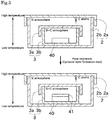
- FIG. 3 is cross-sectional schematic views illustrating a process of causing an epitaxial layer to grow using the TaC container 2 and the SiC container 3.
- the high-temperature vacuum furnace 11 includes a main heating chamber 21 capable of heating an object (e.g., an underlying substrate) to temperatures of 1000°C or more and 2300°C or less and a preheating chamber 22 capable of preheating the object to temperatures of 500°C or more.
- the preheating chamber 22 is disposed below the main heating chamber 21, and adjacent to the main heating chamber 21 vertically (in top-bottom directions).
- the high-temperature vacuum furnace 11 includes a heat insulating chamber 23 disposed below the preheating chamber 22.
- the heat insulating chamber 23 is vertically adjacent to the preheating chamber 22.
- the high-temperature vacuum furnace 11 includes a vacuum chamber 19.
- the main heating chamber 21 and the preheating chamber 22 are disposed inside the vacuum chamber 19.
- the vacuum chamber 19 is connected to a turbo-molecular pump 34 serving as a vacuum generator, and a vacuum of 10 -2 Pa or less and preferably 10 -7 Pa or less, for example, can be obtained in the vacuum chamber 19.
- a gate valve 25 is disposed between the turbo-molecular pump 34 and the vacuum chamber 19.
- the turbo-molecular pump 34 is connected to an auxiliary rotary pump 26.
- the high-temperature vacuum furnace 11 includes a movement mechanism 27 capable of moving the object vertically between the preheating chamber 22 and the main heating chamber 21.
- the movement mechanism 27 includes a support 28 capable of supporting the object and a cylinder 29 capable of moving the support 28 vertically.
- the cylinder 29 includes a cylinder rod 30, and one end of the cylinder rod 30 is coupled to the support 28.
- the high-temperature vacuum furnace 11 is provided with a vacuum gauge 31 for measuring the degree of vacuum and a mass spectrometer 32 for mass spectrometry.
- the vacuum chamber 19 is connected to an unillustrated stock room for storing the object through a transport path 65.
- the transport path 65 can be opened and closed by a gate valve 66.
- the main heating chamber 21 has a regular hexagon shape in cross-sectional plan view, and is disposed in an upper portion of the internal space of the vacuum chamber 19. As illustrated in FIG. 2 , the main heating chamber 21 incorporates a mesh meter 33 as a heater.
- a first multilayer heat reflection metal plate 71 is fixed to a side wall and a ceiling of the main heating chamber 21, and is configured to reflect heat of the mesh meter 33 toward the center of the main heating chamber 21.
- a layout is made in the main heating chamber 21, in which the mesh heater 33 is disposed to surround the object as a heat treatment object, and the multilayer heat reflection metal plate 71 is disposed outside the mesh meter 33.
- the mesh meter 33 is configured to have its width increase toward the top, for example, or is configured such that electric power to be supplied increases toward the top. Accordingly, a temperature gradient can be provided in the main heating chamber 21.
- the temperature of the main heating chamber 21 can be increased to temperatures of 1000°C or more and 2300°C or less, for example.
- the ceiling of the main heating chamber 21 is closed by the first multilayer heat reflection metal plate 71, whereas a through hole 55 is formed in the first multilayer heat reflection metal plate 71 at the bottom.
- the object can move through the through hole 55 between the main heating chamber 21 and the preheating chamber 22 adjacent to the bottom of the main heating chamber 21.
- the support 28 has a configuration in which a second multilayer heat reflection metal plate 72, a third multilayer heat reflection metal plate 73, and a fourth multilayer heat reflection metal plate 74 are arranged in this order from the top with intervals.
- the three multilayer heat reflection metal plates 72 through 74 are each oriented horizontally and are coupled to one another by a column 35 oriented vertically.
- a receiver 36 is disposed in space sandwiched between the second multilayer heat reflection metal plate 72 and the third multilayer heat reflection metal plate 73 so that the TaC container 2 housing the object can be placed on the receiver 36.
- the receiver 36 is made of tantalum carbide.
- An end of the cylinder rod 30 of the cylinder 29 has a flange that is fixed to a lower surface of the fourth multilayer heat reflection metal plate 74.
- the preheating chamber 22 is formed by surrounding space below the main heating chamber 21 by multilayer heat reflection metal plates 76.
- the preheating chamber 22 is configured to have a circular shape in cross-sectional plan view.
- the preheating chamber 22 does not include a heater such as the mesh meter 33.
- a through hole 56 is formed in the multilayer heat reflection metal plate 76 at the bottom of the preheating chamber 22.
- a passage hole 50 is formed in a portion of the multilayer heat reflection metal plate 76 constituting a side wall of the preheating chamber 22, the portion facing the transport path 65.
- the high-temperature vacuum furnace 11 also includes an opening/closing member 51 that can close the passage hole 50.
- the heat insulating chamber 23 disposed adjacent to the bottom of the preheating chamber 22 is defined by the multilayer heat reflection metal plate 76 at the top and by multilayer heat reflection metal plates 77 at the bottom and the side.
- a through hole 57 is formed in the multilayer heat reflection metal plate 77 covering the bottom of the heat insulating chamber 23 so that the cylinder rod 30 can be inserted therethrough.
- the multilayer heat reflection metal plate 77 has a housing recess 58 at a position corresponding to the upper end of the through hole 57.
- the housing recess 58 can accommodate the fourth multilayer heat reflection metal plate 74 of the support 28.
- Each of the multilayer heat reflection metal plates 71 through 74, 76, and 77 has a structure in which metal plates (made of tungsten) are stacked with predetermined intervals.
- a multilayer heat reflection metal plate having a similar structure is used for a portion closing the passage hole 50.
- any material may be used as long as the material has sufficient heating properties to thermal radiation of the mesh meter 33 and has a melting point higher than an ambient temperature.
- a high-melting-point metal material such as tantalum, niobium, or molybdenum may be used for the multilayer heat reflection metal plates 71 through 74, 76, and 77.
- Carbides such as tungsten carbide, zirconium carbide, tantalum carbide, hafnium carbide, and molybdenum carbide may be used as the multilayer heat reflection metal plates 71 through 74, 76, and 77. Reflection surfaces of the multilayer heat reflection metal plates 71 through 74, 76, and 77 may be further provided with an infrared reflection film of, for example, gold or tungsten carbide.
- Each of the multilayer heat reflection metal plates 72 through 74 of the support 28 has a structure in which perforated-metal tungsten plates each having a large number of small through holes are stacked with predetermined intervals with the through holes displaced from one another.
- the number of stacked layers of the second multilayer heat reflection metal plate 72 at the uppermost layer of the support 28 is smaller than that of the first multilayer heat reflection metal plate 71 of the main heating chamber 21.
- the object is introduced from the transport path 65 into the vacuum chamber 19 and is placed on the receiver 36 in the preheating chamber 22.
- the mesh meter 33 is then driven in this state, the main heating chamber 21 is heated to a predetermined temperature of 1000°C or more and 2300°C or less (e.g., about 1900°C).
- the driving of the turbo-molecular pump 34 adjusts the pressure in the vacuum chamber 19 to 10 -3 Pa or less and preferably 10 -5 Pa or less.
- the number of stacked layers of the second multilayer heat reflection metal plate 72 of the support 28 is smaller than that of the first multilayer heat reflection metal plate 71.
- a part of heat generated by the mesh meter 33 is appropriately supplied (distributed) to the preheating chamber 22 through the second multilayer heat reflection metal plate 72 so that the object in the preheating chamber 22 can be preheated to a predetermined temperature of 500°C or more (e.g., 800°C). That is, preheating can be achieved without a heater in the preheating chamber 22, and the configuration of the preheating chamber 22 can be simplified.
- the preheat treatment described above is performed in a predetermined time, and then, the cylinder 29 is driven to lift the support 28. Consequently, the object passes through the through hole 55 from below and moves into the main heating chamber 21. As a result, a main heat treatment starts immediately, and the temperature of the object in the main heating chamber 21 can be rapidly increased to a predetermined temperature (about 1900°C).
- the TaC container 2 is a fitted container including an upper container 2a and a lower container 2b that can be fitted to each other. With this configuration, although the internal space of the TaC container 2 is sealed, a small amount of gas atoms can move from the inside of the TaC container 2 to the outside (or in the opposite direction).
- the TaC container 2 is configured to exert C-atom adsorption ion pump function described later in the case of performing a high-temperature treatment under vacuum.
- the TaC container 2 is made of a tantalum metal and is configured to expose a tantalum carbide layer in the internal space.
- the TaC container 2 is configured such that a TaC layer is formed as the innermost layer (layer closest to the object), a Ta 2 C layer is formed outside the TaC layer, and a tantalum metal as a base material is formed outside the Ta 2 C layer.
- the TaC container 2 shows the function of continuously adsorbing carbon atoms from a surface of the tantalum carbide layer and taking the carbon atoms therein.
- the TaC container 2 of this embodiment has the C-atom adsorption ion pump function (ion getter function).
- the innermost TaC layer is supplemented with Si.
- Si supplemented to this TaC layer is sublimated, and Si vapor is generated.
- Si vapor and C vapor contained in the atmosphere in the TaC container 2 only the C vapor is selectively occluded in the TaC container 2, and thus, the atmosphere in the TaC container 2 can be maintained as a high-purity Si atmosphere.
- a source of Si is not limited to the structure that supplies Si to an inner wall of the TaC container 2, and the inner wall of the TaC container 2 may be made of Ta x Si y (e.g., TaSi 2 or Ta 5 Si 3 ) or other Si compounds, for example. Alternatively, solid Si (Si pellet) may be disposed in the TaC container 2.
- the SiC container 3 is configured to include polycrystalline SiC such as 3C-SiC.
- the entire SiC container 3 is constituted by SiC.
- a part (e.g., inner surface) of the SiC container 3 may be made of polycrystalline SiC as long as Si vapor and C vapor are generated in the internal space during the heat treatment.
- the SiC container 3 is a fitted container including an upper container 3a and a lower container 3b that can be fitted to each other, in the same manner as the TaC container 2. With this configuration, although the internal space of the SiC container 3 is sealed, a small amount of gas atoms can move from the inside of the SiC container 3 to the outside (or in the opposite direction). Accordingly, Si vapor generated in the TaC container 2 moves from the outside of the SiC container 3 to the inside of the SiC container 3 so that Si vapor can be supplied to the internal space of the SiC container 3. As illustrated in FIG. 3 , since the SiC container 3 is placed in the TaC container 2, the SiC container 3 is smaller in size than the TaC container 2.
- the SiC container 3 houses at least one underlying substrate 40.
- the underlying substrate 40 is a substrate serving as a base or an underlying layer for forming an epitaxial layer 41.
- the underlying substrate 40 may be a SiC substrate or may be a substrate of a material except SiC (e.g., an Al compound or a N compound).
- SiC substrate e.g., an Al compound or a N compound.
- crystalline polymorphism is optional, and may be 3C-SiC, 4H-SiC, or 6H-SiC, for example.
- the off-angle (see FIG. 5 ) relative to the ⁇ 11-20> direction or the ⁇ 1-100> direction may be 1° or less or larger than 1°.
- the epitaxial layer 41 may be formed on any one of the Si surface and the C surface of the underlying substrate 40.
- the epitaxial layer 41 of single crystalline 3C-SiC is formed on the underlying substrate 40 by a vapor-phase epitaxial growth method.
- the underlying substrate 40 is housed in the SiC container 3, and the SiC container 3 is further housed in the TaC container 2.
- a temperature gradient is provided in such a manner that the temperature in an upper portion of the TaC container 2 (where the epitaxial layer 41 is formed) is high.
- the temperature gradient is preferably 2°C/mm or less, and more preferably about 1°C/mm. In this state, the TaC container 2 is heated at a temperature of 1600°C or more and 2300°C or less.
- Si supplied to the inner surface of the TaC container 2 is sublimated, and the inside of the TaC container 2 has an equilibrium vapor pressure of Si.
- sublimation of Si makes the inside of the TaC container 2 at an equilibrium vapor pressure of Si.
- the SiC container 3 is heated at high temperatures under a Si vapor pressure, and thus, the SiC container 3 is subjected to etching (Si vapor pressure etching). Specifically, the following reaction is performed. To put it briefly, by heating SiC under a Si vapor pressure, SiC is sublimated as Si 2 C or SiC 2 , for example, through thermal decomposition and chemical reaction with Si. In the SiC container 3, a high C partial pressure is generated, and the C component is transferred to the surface of the underlying substrate 40 using a temperature gradient of 2°C/mm or less as a driving force, and 3C-SiC is crystallized.
- the SiC container 3 is subjected to Si vapor pressure etching so that carbonization of the SiC container 3 can be prevented and C atoms (or the C compound) can be sublimated from the SiC container 3.
- the TaC container 2 has the C-atom adsorption ion pump function as described above, the space inside the TaC container 2 and outside the SiC container 3 has a high-purity Si atmosphere.
- C atoms are not absorbed in the inside of the SiC container 3, and thus, the inside of the SiC container 3 has a C atmosphere.
- Si vapor generated from the Si source of the TaC container 2 also enters the inside of the SiC container 3 through a gap between the upper container 3a and the lower container 3b of the SiC container 3.
- the inside of the SiC container 3 has a Si+C atmosphere.
- the epitaxial layer 41 of single crystalline 3C-SiC can be formed on the surface of the underlying substrate 40 (epitaxial layer growth step). In this manner, a substrate with the epitaxial layer can be produced.
- 3C-SiC is configured such that Si atoms and C atoms are stacked, and a monomolecular layer of Si and C has a height of 0.25 nm.
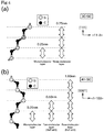
- 4H-SiC the direction of sequence is reversed at every two molecular layers as illustrated FIG. 4(b) , whereas in 3C-SiC, the direction of sequence is not reversed and is uniform.
- the underlying substrate 40 is covered with the TaC container 2 and the SiC container 3 as described above so that the partial pressure of C vapor in the SiC container 3 can be increased.
- the epitaxial layer 41 is allowed to grow sufficiently.
- a wider range of temperature gradient is necessary for obtaining an effective growth velocity.
- a precise heater and fine control are needed, which leads to an increase in manufacturing costs.
- this embodiment only requires that the temperature gradient be 2°C/mm or less, about 1°C/mm, or 1°C/mm or less, and thus, manufacturing costs can be reduced.
- the epitaxial layer 41 of single crystalline 3C-SiC can be formed even using an underlying substrate 40 of a material except SiC.
- the epitaxial layer 41 of single crystalline 3C-SiC can also be formed using an underlying substrate 40 of a material except 3C-SiC.
- SiC can grow on 4H-SiC using an MBE (molecular beam epitaxy) technique and a CVD (chemical vapor deposition) technique.
- MBE mo beam epitaxy
- CVD chemical vapor deposition
- a sublimation proximity method is expected to have a high growth temperature and a high growth velocity, but has poor uniformity in a substrate surface.
- the method of this embodiment is suitable for a heat treatment at high temperatures of 1600°C or more, and epitaxial growth of SiC is performed in a semi-closed system of the Poly-SiC container, and thus, has high uniformity.
- the off-angle of the SiC substrate is large (e.g., larger than 1°)
- step flow growth occurs so that crystalline polymorphism of the underlying substrate 40 can be easily propagated.
- 4H-SiC as the epitaxial layer 41 grows on 4H-SiC as the underlying substrate 40.
- the off-angle of the SiC substrate is preferably small (e.g., 1° or less).
- FIG. 7 shows results of this experiment.
- FIG. 7(a) is a micrograph of the Si surface and the C surface of the epitaxial layer 41 in the case of epitaxial growth performed by placing the SiC container 3 outside the TaC container 2.
- FIG. 7(b) is a micrograph of the Si surface and the C surface of the epitaxial layer 41 in the case of epitaxial growth performed by placing the SiC container 3 inside the TaC container 2.
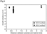
- FIG. 8 In this experiment, the underlying substrate 40 was placed in various environments, and heated at 1800°C with a temperature gradient of about 1°C/mm to compare the amount of growth of the epitaxial layer 41. In particular, the experiment was conducted with variations of a distance L from the surface of the underlying substrate 40 to the material (the SiC container 3 or a polycrystalline SiC plate 45).
- the experiment was conducted with variations of a distance L from the surface of the underlying substrate 40 to the material (the SiC container 3 or a polycrystalline SiC plate 45).
- FIGs. 8(a) and 8(b) one underlying substrate 40 is housed in one SiC container 3
- FIGs. 8(c) and 8(d) two underlying substrates 40 are housed in one SiC container 3.
- FIG. 8 does not show the TaC container 2, each SiC container 3 is housed in the TaC container 2.
- FIG. 9 shows results of this experiment.
- FIG. 9 is a graph showing a correspondence between a distance L from the surface of the underlying substrate 40 to a material and a growth velocity of the epitaxial layer 41 formed on the underlying substrate 40 in each of the underlying substrates 40 used in FIGs. 8(a) through 8(d) .
- all the underlying substrates 40 have substantially the same growth velocity.
- the epitaxial layer 41 is uniformly formed independently of the position in the SiC container 3.
- FIGs. 8(c) and 8(d) by housing the plurality of underlying substrates 40 in one SiC container 3, the epitaxial layer 41 can be efficiently formed.
- the growth velocity of the epitaxial layer 41 is 6 to 8 ⁇ m/h at 1800°C, which is six to eight times as high as that in the CVD method of PTL 1.
- the heating temperature can be 1800°C or more, and thus, a higher growth velocity can be achieved.
- the temperature gradient may be further increased to be higher than 1°C/mm. This can achieve a higher growth velocity.
- the TaC container 2 of this embodiment can be used not only for the process of forming the epitaxial layer 41 but also for the process of etching the underlying substrate 40 (SiC substrate).
- SiC substrate the inside of the TaC container 2 can be maintained in a high-purity Si atmosphere, as illustrated in FIG. 10 , a SiC substrate directly (without interposition of the SiC container 3) disposed in the TaC container 2 can be etched by heating at 1600°C or more (the Si vapor pressure etching).
- the etching step may be performed at any time, and may be performed in order to planarize a SiC substrate after being cut out from an ingot and subjected to mechanical polishing (i.e., before formation of the epitaxial layer 41) or in order to planarize the epitaxial layer 41 roughened by injection of ions (impurity) (i.e., after formation of the epitaxial layer 41), for example.
- vapor-phase epitaxial growth is performed with the SiC container 3 housed in the TaC container 2 and the underlying substrate 40 housed in the SiC container 3 so that single crystalline 3C-SiC is caused to grow as the epitaxial layer 41 on the underlying substrate 40.
- single crystal 4H-SiC or single crystal 6H-SiC for example, can be caused to grow as an epitaxial layer 41 on the underlying substrate 40.
- Crystalline polymorphism of the epitaxial layer 41 to grow can be selected by changing the off-angle and the temperature, for example, of the underlying substrate 40.
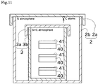
- FIG. 11 illustrates an embodiment in which a plurality of underlying substrates 40 are housed in one SiC container 3 that is housed in a TaC container 2.
- the epitaxial layers 41 of single crystalline 3C-SiC having similar growth velocities and qualities can be formed independently of the position of the SiC container 3 by using the method of an aspect of the present invention, substrates with the epitaxial layers 41 can be efficiently formed.
- the TaC container 2 in a state in which the SiC container 3 of a material including polycrystalline SiC is housed in the TaC container 2 of a material including TaC and the underlying substrates 40 are housed in this SiC container 3, the TaC container 2 is heated with a temperature gradient in such a manner that the inside of the TaC container 2 is at a Si vapor pressure. Consequently, C atoms sublimated by etching of the inner surface of the SiC container 3 are bonded to Si atoms in an atmosphere in the SiC container 3, and thereby, the epitaxial layers 41 of single crystalline SiC (e.g., 3C-SiC, 4H-SiC, or 6H-SiC) grows on the underlying substrates 40.
- the epitaxial layers 41 of single crystalline SiC e.g., 3C-SiC, 4H-SiC, or 6H-SiC
- a high-purity epitaxial layer 41 of single crystalline SiC can be formed at high velocity.
- the material for the epitaxial layers 41 is the SiC container 3, the epitaxial layers 41 are allowed to grow uniformly, as compared to, for example, CVD in which a source gas is introduced.
- a material for the underlying substrate 40 may be an Al compound or a N compound
- a material for the epitaxial layer 41 may be SiC
- an off-angle to the ⁇ 11-20> direction or the ⁇ 1-100> direction may be 1° or less.
- the underlying substrate 40 is not limited to SiC, and thus, a versatile epitaxial growth method can be achieved.
- the underlying substrate 40 is SiC and the off-angle is small, a terrace expands, and a high-quality epitaxial layer of single crystalline SiC can be easily formed independently of crystalline polymorphism of the underlying substrate 40.
- the temperature gradient is preferably 2°C/mm or less.
- the pressure of C atoms in the SiC container 3 is increased, and thus, an epitaxial layer is allowed to grow sufficiently even with a small temperature difference as described above.
- the heater and heating control can be simplified.
- the plurality of underlying substrates 40 are placed in the SiC container 3 and the epitaxial layer 41 is caused to grow on each of the plurality of underlying substrates 40.
- the epitaxial layers 41 can be formed at the same time on the plurality of underlying substrates 40, and therefore the process can be performed efficiently.
- the use of the method of the aspect of the present invention enables the epitaxial layer 41 to be formed uniformly independently of the position in the SiC container 3, and thus, quality does not degrade.
- the inner surface of the TaC container 2 is made of Si or a Si compound, and Si atoms are sublimated from the inner surface of the TaC container 2 by heating during growth of the epitaxial layer 41 so that the inside of the TaC container 2 is at a Si vapor pressure.
- a labor of an operator can be alleviated, as compared to a method of placing solid Si or the like in the TaC container 2.
- a uniform Si atmosphere can be obtained.
- the shapes of the TaC container 2 and the SiC container 3 described above are examples, and may be changed as appropriate.
- the TaC container 2 and the SiC container 3 may have different shapes or may have the same (analogous) shape.
- the TaC container 2 or the SiC container 3 may have a plurality of spaces.
- One TaC container 2 may house a plurality of SiC containers 3, and each of the SiC containers 3 may house a plurality of underlying substrates 40 so that the epitaxial layers 41 can be formed thereon.
- an inert gas e.g., an Ar gas
- an inert gas may be introduced during formation of the epitaxial layer 41 to reduce the growth velocity of the epitaxial layer 41.
- Atmospheres of the internal space of the TaC container 2 and the internal space of the SiC container 3 vary depending on the amount of the Si source, the degree of carbon adsorption function of TaC, the volume of the TaC container 2, the volume of the SiC container 3, and so forth. Thus, by making these factors different from one another, the growth velocity and quality, for example, of the epitaxial layer 41 can be controlled.
Abstract
Description
- The present invention mainly relates to a method for vapor-phase growth of an epitaxial layer of single crystalline SiC on an underlying substrate.
- As a material for semiconductor waters, silicon carbide (SiC) has attracted attention in recent years. SiC has high mechanical strength and high radiation resistance. In addition, SiC shows high valence controlability of electrons and holes by adding an impurity and has features in a wide forbidden band width (e.g., 2.2 eV in 3C-type single crystalline SiC), a high breakdown field, and a high saturated drift velocity of electrons. For such reasons, SiC has been hopefully expected as a material for next-generation power devices capable of achieving high temperature, high frequency, high withstand voltage, and high environmental resistance, which cannot be achieved by existing semiconductor materials. Furthermore, SiC has attracted attention as a substrate for a light-emitting diode (LED).
- A technique for forming an epitaxial layer has been known in a method for producing a semiconductor water using SiC.
Patent Literatures 1 and 2 (PTLs 1 and 2) disclose methods for forming SiC epitaxial layers. -
PTL 1 describes that the SiC epitaxial layer is formed by chemical vapor deposition (CVD). In the process of causing the epitaxial layer to grow, a defect generation suppression layer whose growth velocity is reduced to 1 µm/h or less is introduced so that an epitaxial layer with a small amount of defects can be formed. - Another known technique for causing an epitaxial layer to grow is as follows. This method for forming an epitaxial layer includes the step of causing SiC bulk crystal to grow using a seed crystal addition and sublimation technique and the step of causing liquid-phase growth of an epitaxial layer on a bulk crystal surface. In the step of causing an epitaxial layer to glow, a liquid-phase growth is performed so that micropipe defects having propagated from the seed crystal to the bulk crystal substrate are closed, which achieves formation of a SiC epitaxial layer containing a small amount of micropipe defects.
- PTL1:
Japanese Patent Application Laid-Open No. 2007-284298 - However, the CVD method of
PTL 1 has a low growth velocity, and thus, the process period is long especially in a case of forming a relatively thick epitaxial layer. Thus, this method increases manufacturing costs, and therefore, is not suitable for mass production. In a case of employing the CVD method, the amount of supply of a source gas varies depending on the height and place, for example, of the substrate, and thus, the growth velocity can be nonuniform. - In the method using the seed crystal addition and sublimation technique described above, in the step of causing the epitaxial layer to grow, an element for increasing solubility of an melted material obtained by melting SiC is mixed in a silicon melt. Thus, this element might be unintentionally mixed in epitaxial crystal, and different polymorphs might also be mixed because of a high solvent (carbon) concentration in the silicon melt. As a result, a failure might occur in forming a high-purity epitaxial layer.
- The present invention has been made in view of the circumstances described above, and a primary object of the present invention is to provide a method for forming a SiC epitaxial layer with high purity in a short time.
- Problems to be solved by the present invention are as described above. Solutions to the problems and advantageous effects thereof will now be described.
- A first aspect of the present invention provides a vapor-phase epitaxial growth method as follows. Specifically, in a state in which a SiC container of a material including polycrystalline SiC is housed in a TaC container of a material including TaC and in which an underlying substrate is housed in the SiC container, the TaC container is heated with a temperature gradient such that inside of the TaC container is at a Si vapor pressure. Consequently, C atoms sublimated by etching of the inner surface of the SiC container are bonded to Si atoms in an atmosphere, thereby performing an epitaxial layer growth step of causing an epitaxial layer of single crystalline SiC to grow on the underlying substrate.
- In addition, since SiC has high heat resistance, the process temperature in heating can be increased to about 2000°C, and thus, a high-purity SiC epitaxial layer can be formed in a short time. Furthermore, since a material for the epitaxial layer is the SiC container, the epitaxial layer can be caused to grow uniformly, as compared to, for example, CVD in which a source gas is introduced.
- In the vapor-phase epitaxial growth method, a material for the underlying substrate is preferably an Al compound or a N compound.
- Accordingly, with the method of an aspect of the present invention, the underlying substrate is not limited to SiC, and thus, a versatile epitaxial growth method can be obtained.
- In the vapor-phase epitaxial growth method, a material for the underlying substrate may be SiC, and an off-angle to a <11-20> direction or a <1-100> direction may be 1° or less.
- As a result, in a case where the underlying substrate is SiC and the off-angle is small, a terrace expands, and a high-quality epitaxial layer of SiC can be easily formed independently of crystalline polymorphism of the underlying substrate.
- In the vapor-phase epitaxial growth method, in the epitaxial layer growth step, the temperature gradient is preferably 2°C/mm or less.
- Thus, with the method of an aspect of the present invention, the pressure of C atoms in the SiC container increases, and thus, an epitaxial layer is allowed to grow sufficiently even with a small temperature gradient as described above. As a result, the heater and heating control can be simplified.
- In the vapor-phase epitaxial growth method, in the epitaxial layer growth step, the underlying substrate preferably includes a plurality of underlying substrates placed in the SiC container so that the epitaxial layer is formed on each of the plurality of underlying substrates.
- Accordingly, the epitaxial layers can be formed at the same time on the plurality of underlying substrates, and thus, the process can be performed efficiently. In particular, the use of the method of the aspect of the present invention enables the epitaxial layer to be uniformly formed independently of the position in the SiC container, and thus, quality does not degrade.
- Preferably, in the vapor-phase epitaxial growth method, an inner surface of the TaC container is preferably Si or a Si compound and heating in growth of the epitaxial layer sublimates Si atoms from the inner surface of the TaC container so that inside of the TaC container is at a Si vapor pressure.
- Accordingly, a labor of an operator can be alleviated, as compared to a method of placing solid Si or the like in the TaC container. In addition, by forming Si or the like over a wide range of the inner surface of TaC, a uniform Si atmosphere can be obtained.
- In the vapor-phase epitaxial growth method, crystalline polymorphism of the epitaxial layer is preferably 3C-SiC.
- Alternatively, in the vapor-phase epitaxial growth method, crystalline polymorphism of the epitaxial layer may be 4H-SiC or 6H-SiC.
- Accordingly, epitaxial layers of various types of crystalline polymorphism are allowed to grow with advantages of some aspects of the present invention.
- A second aspect of the present invention provides a method for producing a substrate with an epitaxial layer using the vapor-phase epitaxial growth method described above.
- With this method, a substrate with a high-purity epitaxial layer can be efficiently produced.
- The method for producing a substrate with an epitaxial layer is preferably as follows. The underlying substrate is made of SiC. The underlying substrate is housed in the TaC container without interposition of a SiC container and is heated under a Si vapor pressure, thereby etching the underlying substrate.
- In this manner, the TaC container can be used not only for forming the epitaxial layer but also for etching.
-
- [
FIG. 1 ] A schematic view illustrating a high-temperature vacuum furnace for use in a heat treatment. - [
FIG. 2 ] A cross-sectional structural drawing illustrating a main heating chamber and a preheating chamber of the high-temperature vacuum furnace in detail. - [
FIG. 3 ] Cross-sectional schematic views illustrating a process of causing an epitaxial layer to grow using a TaC container and a SiC container. - [
FIG. 4 ] Cross-sectional schematic views for describing atomic arrangements and stacking periods of 3C-SiC single crystal and 4H-SiC single crystal. - [
FIG. 5 ] A view illustrating an off-angle of a SiC substrate. - [
FIG. 6 ] A view illustrating a state in which an epitaxial layer grows with SiC containers disposed inside and outside of a TaC container. - [
FIG. 7 ] Micrographs showing a Si surface and a C surface of an epitaxial layer that has grown with SiC containers disposed inside and outside of a TaC container. - [
FIG. 8 ] Cross-sectional schematic views illustrating four patterns of heat treatment with different treatment conditions (especially a distance from an underlying substrate to a material). - [
FIG. 9 ] A graph showing a relationship between the position of an underlying substrate and a growth velocity. - [
FIG. 10 ] Cross-sectional schematic views illustrating a process of performing etching using TaC. - [
FIG. 11 ] A cross-sectional schematic view illustrating a state in which 3C-SiC epitaxial layers are formed at the same time on a plurality of underlying substrates. - Hereinafter, an embodiment of the present invention will be described with reference to the drawings.
- First, referring to
FIGs. 1 through 3 , a high-temperature vacuum furnace 11, aTaC container 2, and aSiC container 3 for performing a heat treatment will be described.FIG. 1 is a schematic view illustrating the high-temperature vacuum furnace 11 for use in a heat treatment.FIG. 2 is a cross-sectional view illustrating a main heating chamber and a preheating chamber of the high-temperature vacuum furnace 11 in detail.FIG. 3 is cross-sectional schematic views illustrating a process of causing an epitaxial layer to grow using theTaC container 2 and theSiC container 3. - As illustrated in
FIGs. 1 and2 , the high-temperature vacuum furnace 11 includes amain heating chamber 21 capable of heating an object (e.g., an underlying substrate) to temperatures of 1000°C or more and 2300°C or less and a preheatingchamber 22 capable of preheating the object to temperatures of 500°C or more. The preheatingchamber 22 is disposed below themain heating chamber 21, and adjacent to themain heating chamber 21 vertically (in top-bottom directions). The high-temperature vacuum furnace 11 includes aheat insulating chamber 23 disposed below the preheatingchamber 22. Theheat insulating chamber 23 is vertically adjacent to the preheatingchamber 22. - The high-
temperature vacuum furnace 11 includes avacuum chamber 19. Themain heating chamber 21 and the preheatingchamber 22 are disposed inside thevacuum chamber 19. Thevacuum chamber 19 is connected to a turbo-molecular pump 34 serving as a vacuum generator, and a vacuum of 10-2 Pa or less and preferably 10-7 Pa or less, for example, can be obtained in thevacuum chamber 19. Agate valve 25 is disposed between the turbo-molecular pump 34 and thevacuum chamber 19. The turbo-molecular pump 34 is connected to an auxiliaryrotary pump 26. - The high-
temperature vacuum furnace 11 includes amovement mechanism 27 capable of moving the object vertically between the preheatingchamber 22 and themain heating chamber 21. Themovement mechanism 27 includes asupport 28 capable of supporting the object and acylinder 29 capable of moving thesupport 28 vertically. Thecylinder 29 includes acylinder rod 30, and one end of thecylinder rod 30 is coupled to thesupport 28. The high-temperature vacuum furnace 11 is provided with avacuum gauge 31 for measuring the degree of vacuum and amass spectrometer 32 for mass spectrometry. - The
vacuum chamber 19 is connected to an unillustrated stock room for storing the object through atransport path 65. Thetransport path 65 can be opened and closed by agate valve 66. - The
main heating chamber 21 has a regular hexagon shape in cross-sectional plan view, and is disposed in an upper portion of the internal space of thevacuum chamber 19. As illustrated inFIG. 2 , themain heating chamber 21 incorporates amesh meter 33 as a heater. A first multilayer heatreflection metal plate 71 is fixed to a side wall and a ceiling of themain heating chamber 21, and is configured to reflect heat of themesh meter 33 toward the center of themain heating chamber 21. - In this manner, a layout is made in the
main heating chamber 21, in which themesh heater 33 is disposed to surround the object as a heat treatment object, and the multilayer heatreflection metal plate 71 is disposed outside themesh meter 33. Themesh meter 33 is configured to have its width increase toward the top, for example, or is configured such that electric power to be supplied increases toward the top. Accordingly, a temperature gradient can be provided in themain heating chamber 21. The temperature of themain heating chamber 21 can be increased to temperatures of 1000°C or more and 2300°C or less, for example. - The ceiling of the
main heating chamber 21 is closed by the first multilayer heatreflection metal plate 71, whereas a throughhole 55 is formed in the first multilayer heatreflection metal plate 71 at the bottom. The object can move through the throughhole 55 between themain heating chamber 21 and the preheatingchamber 22 adjacent to the bottom of themain heating chamber 21. - A part of the
support 28 of themovement mechanism 27 is inserted in the throughhole 55. Thesupport 28 has a configuration in which a second multilayer heatreflection metal plate 72, a third multilayer heatreflection metal plate 73, and a fourth multilayer heatreflection metal plate 74 are arranged in this order from the top with intervals. - The three multilayer heat
reflection metal plates 72 through 74 are each oriented horizontally and are coupled to one another by acolumn 35 oriented vertically. Areceiver 36 is disposed in space sandwiched between the second multilayer heatreflection metal plate 72 and the third multilayer heatreflection metal plate 73 so that theTaC container 2 housing the object can be placed on thereceiver 36. In this embodiment, thereceiver 36 is made of tantalum carbide. - An end of the
cylinder rod 30 of thecylinder 29 has a flange that is fixed to a lower surface of the fourth multilayer heatreflection metal plate 74. With this configuration, when thecylinder 29 is caused to extend and contract, the object on thereceiver 36 can be moved upward and downward together with the three multilayer heatreflection metal plates 72 through 74. - The preheating
chamber 22 is formed by surrounding space below themain heating chamber 21 by multilayer heatreflection metal plates 76. The preheatingchamber 22 is configured to have a circular shape in cross-sectional plan view. The preheatingchamber 22 does not include a heater such as themesh meter 33. - As illustrated in
FIG. 2 , a throughhole 56 is formed in the multilayer heatreflection metal plate 76 at the bottom of the preheatingchamber 22. Apassage hole 50 is formed in a portion of the multilayer heatreflection metal plate 76 constituting a side wall of the preheatingchamber 22, the portion facing thetransport path 65. The high-temperature vacuum furnace 11 also includes an opening/closingmember 51 that can close thepassage hole 50. - The
heat insulating chamber 23 disposed adjacent to the bottom of the preheatingchamber 22 is defined by the multilayer heatreflection metal plate 76 at the top and by multilayer heatreflection metal plates 77 at the bottom and the side. A throughhole 57 is formed in the multilayer heatreflection metal plate 77 covering the bottom of theheat insulating chamber 23 so that thecylinder rod 30 can be inserted therethrough. - The multilayer heat
reflection metal plate 77 has ahousing recess 58 at a position corresponding to the upper end of the throughhole 57. Thehousing recess 58 can accommodate the fourth multilayer heatreflection metal plate 74 of thesupport 28. - Each of the multilayer heat
reflection metal plates 71 through 74, 76, and 77 has a structure in which metal plates (made of tungsten) are stacked with predetermined intervals. In the opening/closingmember 51, a multilayer heat reflection metal plate having a similar structure is used for a portion closing thepassage hole 50. - As a material for the multilayer heat
reflection metal plates 71 through 74, 76, and 77, any material may be used as long as the material has sufficient heating properties to thermal radiation of themesh meter 33 and has a melting point higher than an ambient temperature. Instead of tungsten used above, a high-melting-point metal material such as tantalum, niobium, or molybdenum may be used for the multilayer heatreflection metal plates 71 through 74, 76, and 77. Carbides such as tungsten carbide, zirconium carbide, tantalum carbide, hafnium carbide, and molybdenum carbide may be used as the multilayer heatreflection metal plates 71 through 74, 76, and 77. Reflection surfaces of the multilayer heatreflection metal plates 71 through 74, 76, and 77 may be further provided with an infrared reflection film of, for example, gold or tungsten carbide. - Each of the multilayer heat
reflection metal plates 72 through 74 of thesupport 28 has a structure in which perforated-metal tungsten plates each having a large number of small through holes are stacked with predetermined intervals with the through holes displaced from one another. - The number of stacked layers of the second multilayer heat
reflection metal plate 72 at the uppermost layer of thesupport 28 is smaller than that of the first multilayer heatreflection metal plate 71 of themain heating chamber 21. - In this state, the object is introduced from the
transport path 65 into thevacuum chamber 19 and is placed on thereceiver 36 in the preheatingchamber 22. When themesh meter 33 is then driven in this state, themain heating chamber 21 is heated to a predetermined temperature of 1000°C or more and 2300°C or less (e.g., about 1900°C). At this time, the driving of the turbo-molecular pump 34 adjusts the pressure in thevacuum chamber 19 to 10-3 Pa or less and preferably 10-5 Pa or less. - Here, as described above, the number of stacked layers of the second multilayer heat
reflection metal plate 72 of thesupport 28 is smaller than that of the first multilayer heatreflection metal plate 71. Thus, a part of heat generated by themesh meter 33 is appropriately supplied (distributed) to the preheatingchamber 22 through the second multilayer heatreflection metal plate 72 so that the object in the preheatingchamber 22 can be preheated to a predetermined temperature of 500°C or more (e.g., 800°C). That is, preheating can be achieved without a heater in the preheatingchamber 22, and the configuration of the preheatingchamber 22 can be simplified. - The preheat treatment described above is performed in a predetermined time, and then, the
cylinder 29 is driven to lift thesupport 28. Consequently, the object passes through the throughhole 55 from below and moves into themain heating chamber 21. As a result, a main heat treatment starts immediately, and the temperature of the object in themain heating chamber 21 can be rapidly increased to a predetermined temperature (about 1900°C). - As illustrated in
FIG. 3 , theTaC container 2 is a fitted container including anupper container 2a and alower container 2b that can be fitted to each other. With this configuration, although the internal space of theTaC container 2 is sealed, a small amount of gas atoms can move from the inside of theTaC container 2 to the outside (or in the opposite direction). In addition, theTaC container 2 is configured to exert C-atom adsorption ion pump function described later in the case of performing a high-temperature treatment under vacuum. Specifically, theTaC container 2 is made of a tantalum metal and is configured to expose a tantalum carbide layer in the internal space. - More specifically, the
TaC container 2 is configured such that a TaC layer is formed as the innermost layer (layer closest to the object), a Ta2C layer is formed outside the TaC layer, and a tantalum metal as a base material is formed outside the Ta2C layer. Thus, as long as the high-temperature treatment continues under vacuum as described above, theTaC container 2 shows the function of continuously adsorbing carbon atoms from a surface of the tantalum carbide layer and taking the carbon atoms therein. In this regard, theTaC container 2 of this embodiment has the C-atom adsorption ion pump function (ion getter function). The innermost TaC layer is supplemented with Si. Accordingly, in the heat treatment, Si supplemented to this TaC layer is sublimated, and Si vapor is generated. In Si vapor and C vapor contained in the atmosphere in theTaC container 2, only the C vapor is selectively occluded in theTaC container 2, and thus, the atmosphere in theTaC container 2 can be maintained as a high-purity Si atmosphere. - A source of Si is not limited to the structure that supplies Si to an inner wall of the
TaC container 2, and the inner wall of theTaC container 2 may be made of TaxSiy (e.g., TaSi2 or Ta5Si3) or other Si compounds, for example. Alternatively, solid Si (Si pellet) may be disposed in theTaC container 2. - The
SiC container 3 is configured to include polycrystalline SiC such as 3C-SiC. In this embodiment, theentire SiC container 3 is constituted by SiC. A part (e.g., inner surface) of theSiC container 3 may be made of polycrystalline SiC as long as Si vapor and C vapor are generated in the internal space during the heat treatment. - The
SiC container 3 is a fitted container including anupper container 3a and alower container 3b that can be fitted to each other, in the same manner as theTaC container 2. With this configuration, although the internal space of theSiC container 3 is sealed, a small amount of gas atoms can move from the inside of theSiC container 3 to the outside (or in the opposite direction). Accordingly, Si vapor generated in theTaC container 2 moves from the outside of theSiC container 3 to the inside of theSiC container 3 so that Si vapor can be supplied to the internal space of theSiC container 3. As illustrated inFIG. 3 , since theSiC container 3 is placed in theTaC container 2, theSiC container 3 is smaller in size than theTaC container 2. TheSiC container 3 houses at least oneunderlying substrate 40. - The underlying
substrate 40 is a substrate serving as a base or an underlying layer for forming anepitaxial layer 41. The underlyingsubstrate 40 may be a SiC substrate or may be a substrate of a material except SiC (e.g., an Al compound or a N compound). In the case of the SiC substrate, crystalline polymorphism is optional, and may be 3C-SiC, 4H-SiC, or 6H-SiC, for example. In a case where the underlyingsubstrate 40 is a SiC substrate, the off-angle (seeFIG. 5 ) relative to the <11-20> direction or the <1-100> direction may be 1° or less or larger than 1°. Theepitaxial layer 41 may be formed on any one of the Si surface and the C surface of theunderlying substrate 40. - Next, an epitaxial growth step will be described. In this embodiment, the
epitaxial layer 41 of single crystalline 3C-SiC is formed on theunderlying substrate 40 by a vapor-phase epitaxial growth method. Specifically, as illustrated inFIG. 3 , the underlyingsubstrate 40 is housed in theSiC container 3, and theSiC container 3 is further housed in theTaC container 2. A temperature gradient is provided in such a manner that the temperature in an upper portion of the TaC container 2 (where theepitaxial layer 41 is formed) is high. The temperature gradient is preferably 2°C/mm or less, and more preferably about 1°C/mm. In this state, theTaC container 2 is heated at a temperature of 1600°C or more and 2300°C or less. - With this heat treatment, Si supplied to the inner surface of the
TaC container 2 is sublimated, and the inside of theTaC container 2 has an equilibrium vapor pressure of Si. In the case of using another Si source, sublimation of Si makes the inside of theTaC container 2 at an equilibrium vapor pressure of Si. Accordingly, theSiC container 3 is heated at high temperatures under a Si vapor pressure, and thus, theSiC container 3 is subjected to etching (Si vapor pressure etching). Specifically, the following reaction is performed. To put it briefly, by heating SiC under a Si vapor pressure, SiC is sublimated as Si2C or SiC2, for example, through thermal decomposition and chemical reaction with Si. In theSiC container 3, a high C partial pressure is generated, and the C component is transferred to the surface of theunderlying substrate 40 using a temperature gradient of 2°C/mm or less as a driving force, and 3C-SiC is crystallized. - The
SiC container 3 is subjected to Si vapor pressure etching so that carbonization of theSiC container 3 can be prevented and C atoms (or the C compound) can be sublimated from theSiC container 3. Here, since theTaC container 2 has the C-atom adsorption ion pump function as described above, the space inside theTaC container 2 and outside theSiC container 3 has a high-purity Si atmosphere. On the other hand, C atoms are not absorbed in the inside of theSiC container 3, and thus, the inside of theSiC container 3 has a C atmosphere. In addition, Si vapor generated from the Si source of theTaC container 2 also enters the inside of theSiC container 3 through a gap between theupper container 3a and thelower container 3b of theSiC container 3. Accordingly, the inside of theSiC container 3 has a Si+C atmosphere. Thus, by performing the heat treatment with a temperature gradient, theepitaxial layer 41 of single crystalline 3C-SiC can be formed on the surface of the underlying substrate 40 (epitaxial layer growth step). In this manner, a substrate with the epitaxial layer can be produced. - With reference to
FIG. 4 , molecular sequences of 4H-SiC and 3C-SiC will be briefly described. As illustrated inFIG. 4(a) , 3C-SiC is configured such that Si atoms and C atoms are stacked, and a monomolecular layer of Si and C has a height of 0.25 nm. In 4H-SiC, the direction of sequence is reversed at every two molecular layers as illustratedFIG. 4(b) , whereas in 3C-SiC, the direction of sequence is not reversed and is uniform. - Here, the underlying
substrate 40 is covered with theTaC container 2 and theSiC container 3 as described above so that the partial pressure of C vapor in theSiC container 3 can be increased. Thus, even with a temperature gradient of about 1°C/mm, theepitaxial layer 41 is allowed to grow sufficiently. In a known sublimation technique or other techniques, a wider range of temperature gradient is necessary for obtaining an effective growth velocity. To increase the range of temperature gradient, however, a precise heater and fine control are needed, which leads to an increase in manufacturing costs. In view of this, this embodiment only requires that the temperature gradient be 2°C/mm or less, about 1°C/mm, or 1°C/mm or less, and thus, manufacturing costs can be reduced. - By causing the
epitaxial layer 41 to grow with the technique of this embodiment, theepitaxial layer 41 of single crystalline 3C-SiC can be formed even using anunderlying substrate 40 of a material except SiC. Theepitaxial layer 41 of single crystalline 3C-SiC can also be formed using anunderlying substrate 40 of a material except 3C-SiC. In addition, SiC can grow on 4H-SiC using an MBE (molecular beam epitaxy) technique and a CVD (chemical vapor deposition) technique. The MBE technique and the CVD technique, however, are not suitable for a heat treatment at 1600°C or more, for example, and thus, the growth velocity has an upper limit. On the other hand, a sublimation proximity method is expected to have a high growth temperature and a high growth velocity, but has poor uniformity in a substrate surface. On the other hand, the method of this embodiment is suitable for a heat treatment at high temperatures of 1600°C or more, and epitaxial growth of SiC is performed in a semi-closed system of the Poly-SiC container, and thus, has high uniformity. - In a case where the off-angle of the SiC substrate is large (e.g., larger than 1°), step flow growth occurs so that crystalline polymorphism of the
underlying substrate 40 can be easily propagated. Thus, 4H-SiC as theepitaxial layer 41 grows on 4H-SiC as the underlyingsubstrate 40. Thus, in a case where theepitaxial layer 41 of the 3C-SiC is needed, the off-angle of the SiC substrate is preferably small (e.g., 1° or less). - Next, an experiment for determining advantages in housing the
SiC container 3 in theTaC container 2 will be described with reference toFIGs. 6 and7 . As illustrated inFIG. 6 , in this experiment, theSiC containers 3 were placed inside and outside theTaC container 2, and theepitaxial layer 41 was caused to grow on theunderlying substrate 40 in eachSiC container 3. -
FIG. 7 shows results of this experiment.FIG. 7(a) is a micrograph of the Si surface and the C surface of theepitaxial layer 41 in the case of epitaxial growth performed by placing theSiC container 3 outside theTaC container 2.FIG. 7(b) is a micrograph of the Si surface and the C surface of theepitaxial layer 41 in the case of epitaxial growth performed by placing theSiC container 3 inside theTaC container 2. By disposing theSiC container 3 inside theTaC container 2 in this manner, the surface of theepitaxial layer 41 is planalized, thereby forming a high-quality epitaxial layer 41. The growth velocity also increases about five times in the case of disposing theSiC container 3 inside theTaC container 2. By covering theunderlying substrate 40 with theSiC container 3 and theTaC container 2 in the manner described above, the high-quality epitaxial layer 41 can be formed at high speed. - Thereafter, an experiment for confirming uniform formation of the
epitaxial layer 41 irrespective of the position in theSiC container 3 will be described with reference toFIGs. 8 and9 . As illustrated inFIG. 8 , in this experiment, the underlyingsubstrate 40 was placed in various environments, and heated at 1800°C with a temperature gradient of about 1°C/mm to compare the amount of growth of theepitaxial layer 41. In particular, the experiment was conducted with variations of a distance L from the surface of theunderlying substrate 40 to the material (theSiC container 3 or a polycrystalline SiC plate 45). InFIGs. 8(a) and 8(b) , one underlyingsubstrate 40 is housed in oneSiC container 3, whereas inFIGs. 8(c) and 8(d) , twounderlying substrates 40 are housed in oneSiC container 3. AlthoughFIG. 8 does not show theTaC container 2, eachSiC container 3 is housed in theTaC container 2. -
FIG. 9 shows results of this experiment.FIG. 9 is a graph showing a correspondence between a distance L from the surface of theunderlying substrate 40 to a material and a growth velocity of theepitaxial layer 41 formed on theunderlying substrate 40 in each of theunderlying substrates 40 used inFIGs. 8(a) through 8(d) . As shown inFIG. 9 , all theunderlying substrates 40 have substantially the same growth velocity. Thus, it was confirmed that if the temperature gradient is uniform, theepitaxial layer 41 is uniformly formed independently of the position in theSiC container 3. As illustrated inFIGs. 8(c) and 8(d) , by housing the plurality ofunderlying substrates 40 in oneSiC container 3, theepitaxial layer 41 can be efficiently formed. - As illustrated in
FIG. 9 , the growth velocity of theepitaxial layer 41 is 6 to 8 µm/h at 1800°C, which is six to eight times as high as that in the CVD method ofPTL 1. In the method of this embodiment, the heating temperature can be 1800°C or more, and thus, a higher growth velocity can be achieved. The temperature gradient may be further increased to be higher than 1°C/mm. This can achieve a higher growth velocity. - The
TaC container 2 of this embodiment can be used not only for the process of forming theepitaxial layer 41 but also for the process of etching the underlying substrate 40 (SiC substrate). As described above, since the inside of theTaC container 2 can be maintained in a high-purity Si atmosphere, as illustrated inFIG. 10 , a SiC substrate directly (without interposition of the SiC container 3) disposed in theTaC container 2 can be etched by heating at 1600°C or more (the Si vapor pressure etching). - The etching step may be performed at any time, and may be performed in order to planarize a SiC substrate after being cut out from an ingot and subjected to mechanical polishing (i.e., before formation of the epitaxial layer 41) or in order to planarize the
epitaxial layer 41 roughened by injection of ions (impurity) (i.e., after formation of the epitaxial layer 41), for example. - In the above-described process, vapor-phase epitaxial growth is performed with the
SiC container 3 housed in theTaC container 2 and theunderlying substrate 40 housed in theSiC container 3 so that single crystalline 3C-SiC is caused to grow as theepitaxial layer 41 on theunderlying substrate 40. With a similar process,single crystal 4H-SiC or single crystal 6H-SiC, for example, can be caused to grow as anepitaxial layer 41 on theunderlying substrate 40. Crystalline polymorphism of theepitaxial layer 41 to grow can be selected by changing the off-angle and the temperature, for example, of theunderlying substrate 40. -
FIG. 11 illustrates an embodiment in which a plurality ofunderlying substrates 40 are housed in oneSiC container 3 that is housed in aTaC container 2. As described above, since theepitaxial layers 41 of single crystalline 3C-SiC having similar growth velocities and qualities can be formed independently of the position of theSiC container 3 by using the method of an aspect of the present invention, substrates with theepitaxial layers 41 can be efficiently formed. - As described above, in this embodiment, in a state in which the
SiC container 3 of a material including polycrystalline SiC is housed in theTaC container 2 of a material including TaC and theunderlying substrates 40 are housed in thisSiC container 3, theTaC container 2 is heated with a temperature gradient in such a manner that the inside of theTaC container 2 is at a Si vapor pressure. Consequently, C atoms sublimated by etching of the inner surface of theSiC container 3 are bonded to Si atoms in an atmosphere in theSiC container 3, and thereby, theepitaxial layers 41 of single crystalline SiC (e.g., 3C-SiC, 4H-SiC, or 6H-SiC) grows on theunderlying substrates 40. - Accordingly, a high-
purity epitaxial layer 41 of single crystalline SiC can be formed at high velocity. In addition, since the material for theepitaxial layers 41 is theSiC container 3, theepitaxial layers 41 are allowed to grow uniformly, as compared to, for example, CVD in which a source gas is introduced. - In the vapor-phase epitaxial growth method of this embodiment, a material for the
underlying substrate 40 may be an Al compound or a N compound, a material for theepitaxial layer 41 may be SiC, and an off-angle to the <11-20> direction or the <1-100> direction may be 1° or less. - Accordingly, with the method of an aspect of the present invention, the underlying
substrate 40 is not limited to SiC, and thus, a versatile epitaxial growth method can be achieved. As a result, in a case where the underlyingsubstrate 40 is SiC and the off-angle is small, a terrace expands, and a high-quality epitaxial layer of single crystalline SiC can be easily formed independently of crystalline polymorphism of theunderlying substrate 40. - In the vapor-phase epitaxial growth method of this embodiment, the temperature gradient is preferably 2°C/mm or less.
- Thus, with the method of an aspect of the present invention, the pressure of C atoms in the
SiC container 3 is increased, and thus, an epitaxial layer is allowed to grow sufficiently even with a small temperature difference as described above. As a result, the heater and heating control can be simplified. - In the vapor-phase epitaxial growth method of this embodiment, the plurality of
underlying substrates 40 are placed in theSiC container 3 and theepitaxial layer 41 is caused to grow on each of the plurality ofunderlying substrates 40. - Accordingly, the
epitaxial layers 41 can be formed at the same time on the plurality ofunderlying substrates 40, and therefore the process can be performed efficiently. In particular, the use of the method of the aspect of the present invention enables theepitaxial layer 41 to be formed uniformly independently of the position in theSiC container 3, and thus, quality does not degrade. - In the vapor-phase epitaxial growth method of this embodiment, the inner surface of the
TaC container 2 is made of Si or a Si compound, and Si atoms are sublimated from the inner surface of theTaC container 2 by heating during growth of theepitaxial layer 41 so that the inside of theTaC container 2 is at a Si vapor pressure. - Accordingly, a labor of an operator can be alleviated, as compared to a method of placing solid Si or the like in the
TaC container 2. In addition, by forming Si or the like over a wide range of the inner surface of TaC, a uniform Si atmosphere can be obtained. - The foregoing description is directed to a preferred embodiment of the present invention, and the configuration described above may be changed, for example, as follows.
- The shapes of the
TaC container 2 and theSiC container 3 described above are examples, and may be changed as appropriate. For example, theTaC container 2 and theSiC container 3 may have different shapes or may have the same (analogous) shape. As illustrated inFIG. 8(d) , theTaC container 2 or theSiC container 3 may have a plurality of spaces. OneTaC container 2 may house a plurality ofSiC containers 3, and each of theSiC containers 3 may house a plurality ofunderlying substrates 40 so that theepitaxial layers 41 can be formed thereon. - For example, to control the amount of growth of the
epitaxial layer 41 accurately, an inert gas (e.g., an Ar gas) may be introduced during formation of theepitaxial layer 41 to reduce the growth velocity of theepitaxial layer 41. - Atmospheres of the internal space of the
TaC container 2 and the internal space of the SiC container 3 (especially partial pressures of Si and C) vary depending on the amount of the Si source, the degree of carbon adsorption function of TaC, the volume of theTaC container 2, the volume of theSiC container 3, and so forth. Thus, by making these factors different from one another, the growth velocity and quality, for example, of theepitaxial layer 41 can be controlled. -
- 2
- TaC container
- 2a
- upper container
- 2b
- lower container
- 3
- SiC container
- 3a
- upper container
- 3b
- lower container
- 11
- high-temperature vacuum furnace
- 40
- SiC substrate
- 41
- epitaxial layer
- 45
- polycrystalline SiC plate
- [Item 1]
A vapor-phase epitaxial growth method for performing an epitaxial layer growth step, wherein
in a state in which a SiC container of a material including polycrystalline SiC is housed in a TaC container of a material including TaC and in which an underlying substrate is housed in the SiC container,
the TaC container is heated with a temperature gradient such that inside of the TaC container is at a Si vapor pressure, and
C atoms sublimated by etching of an inner surface of the SiC container are bonded to Si atoms in an atmosphere, thereby causing an epitaxial layer of single crystalline SiC to grow on the underlying substrate. - [Item 2]
The vapor-phase epitaxial growth method according toitem 1, wherein a material for the underlying substrate is an Al compound or a N compound. - [Item 3]
The vapor-phase epitaxial growth method according toitem 1, wherein
a material for the underlying substrate is SiC, and
an off-angle to a <11-20> direction or a <1-100> direction is 1° or less. - [Item 4]
The vapor-phase epitaxial growth method according toitem 1, wherein
in the epitaxial layer growth step, the temperature gradient is 2°C/mm or less. - [Item 5]
The vapor-phase epitaxial growth method according toitem 1, wherein
in the epitaxial layer growth step, the underlying substrate comprises a plurality of underlying substrates, and
the plurality of underlying substrates are placed in the SiC container so that the epitaxial layer grows on each of the underlying substrates. - [Item 6]
The vapor-phase epitaxial growth method according toitem 1, wherein
an inner surface of the TaC container is made of Si or a Si compound, and
heating in growth of the epitaxial layer sublimates Si atoms from the inner surface of the TaC container so that inside of the TaC container is at the Si vapor pressure. - [Item 7]
The vapor-phase epitaxial growth method according toitem 1, wherein
crystalline polymorphism of the epitaxial layer is 3C-SiC. - [Item 8]
The vapor-phase epitaxial growth method according toitem 1, wherein
crystalline polymorphism of the epitaxial layer is 4H-SiC or 6H-SiC. - [Item 9]
A method for producing a substrate with an epitaxial layer, the method using the vapor-phase epitaxial growth method according toitem 1. - [Item 10]
The method for producing a substrate with an epitaxial layer according toitem 9, wherein
a material for the underlying substrate is SiC,
the underlying substrate is housed in the TaC container without interposition of a SiC container and is heated under a Si vapor pressure, thereby etching the underlying substrate.
Claims (10)
- A manufacturing device of SiC semiconductor substrates, the device comprising:a SiC container (3) in which Si vapor and C vapor are generated in the internal space during the heat treatment; anda high-temperature vacuum furnace (11) capable of heating the SiC container in Si atmosphere.
- The manufacturing device of SiC semiconductor substrates according to claim 1, wherein
the SiC container is housed in Si atmosphere and an underlying substrate (40) is housed in the SiC container. - The manufacturing device of SiC semiconductor substrates according to claim 1 or 2, wherein
the high-temperature vacuum furnace is capable of heating with a temperature gradient. - The manufacturing device of SiC semiconductor substrates according to any one of claims 1 to 3, the device further comprising:
a TaC container (2) in which Si vapor is generated in the internal space during the heat treatment. - The manufacturing device of SiC semiconductor substrates according to claim 4, wherein
the SiC container is housed in the TaC container. - A manufacturing device of SiC semiconductor substrates, the device comprising:a SiC container (3) in which Si vapor and C vapor are generated in the internal space during the heat treatment; anda TaC container (2) in which Si vapor is generated in the internal space during the heat treatment.
- The manufacturing device of SiC semiconductor substrates according to claim 6, wherein
the SiC container is housed in TaC container and an underlying substrate (40) is housed in the SiC container. - The manufacturing device of SiC semiconductor substrates according to any one of claims 4 to 7, wherein
the TaC container includes a TaC layer and a source of Si. - The manufacturing device of SiC semiconductor substrates according to any one of claims 1 to 8, wherein
the SiC container is configured to include polycrystalline SiC. - The manufacturing device of SiC semiconductor substrates according to any one of claims 1 to 9, wherein
the underlying substrate comprises a plurality of underlying substrates, and
the plurality of underlying substrates are placed in the SiC container.
Applications Claiming Priority (3)
| Application Number | Priority Date | Filing Date | Title |
|---|---|---|---|
| JP2016092073 | 2016-04-28 | ||
| EP17789663.6A EP3450595B1 (en) | 2016-04-28 | 2017-04-27 | Vapour-phase epitaxial growth method, and method for producing substrate equipped with epitaxial layer |
| PCT/JP2017/016738 WO2017188381A1 (en) | 2016-04-28 | 2017-04-27 | Vapour-phase epitaxial growth method, and method for producing substrate equipped with epitaxial layer |
Related Parent Applications (2)
| Application Number | Title | Priority Date | Filing Date |
|---|---|---|---|
| EP17789663.6A Division EP3450595B1 (en) | 2016-04-28 | 2017-04-27 | Vapour-phase epitaxial growth method, and method for producing substrate equipped with epitaxial layer |
| EP17789663.6A Division-Into EP3450595B1 (en) | 2016-04-28 | 2017-04-27 | Vapour-phase epitaxial growth method, and method for producing substrate equipped with epitaxial layer |
Publications (1)
| Publication Number | Publication Date |
|---|---|
| EP3892761A1 true EP3892761A1 (en) | 2021-10-13 |
Family
ID=60159696
Family Applications (3)
| Application Number | Title | Priority Date | Filing Date |
|---|---|---|---|
| EP21176448.5A Pending EP3892761A1 (en) | 2016-04-28 | 2017-04-27 | Vapour-phase epitaxial growth method, and method for producing substrate equipped with epitaxial layer |
| EP17789663.6A Active EP3450595B1 (en) | 2016-04-28 | 2017-04-27 | Vapour-phase epitaxial growth method, and method for producing substrate equipped with epitaxial layer |
| EP21176449.3A Pending EP3892762A1 (en) | 2016-04-28 | 2017-04-27 | Vapour-phase epitaxial growth method, and method for producing substrate equipped with epitaxial layer |
Family Applications After (2)
| Application Number | Title | Priority Date | Filing Date |
|---|---|---|---|
| EP17789663.6A Active EP3450595B1 (en) | 2016-04-28 | 2017-04-27 | Vapour-phase epitaxial growth method, and method for producing substrate equipped with epitaxial layer |
| EP21176449.3A Pending EP3892762A1 (en) | 2016-04-28 | 2017-04-27 | Vapour-phase epitaxial growth method, and method for producing substrate equipped with epitaxial layer |
Country Status (5)
| Country | Link |
|---|---|
| US (4) | US11359307B2 (en) |
| EP (3) | EP3892761A1 (en) |
| JP (3) | JP6721904B2 (en) |
| CN (3) | CN114351248A (en) |
| WO (1) | WO2017188381A1 (en) |
Families Citing this family (21)
| Publication number | Priority date | Publication date | Assignee | Title |
|---|---|---|---|---|
| CN114351248A (en) | 2016-04-28 | 2022-04-15 | 学校法人关西学院 | Vapor phase epitaxial growth method and preparation method of substrate with epitaxial layer |
| CN113227466A (en) * | 2018-11-05 | 2021-08-06 | 学校法人关西学院 | SiC semiconductor substrate, and method and apparatus for manufacturing same |
| WO2020095872A1 (en) * | 2018-11-05 | 2020-05-14 | 学校法人関西学院 | Sic semiconductor substrate, method for manufacturing same, and device for manufacturing same |
| JP7242990B2 (en) * | 2018-12-03 | 2023-03-22 | 株式会社レゾナック | SiC chemical vapor deposition apparatus and method for manufacturing SiC epitaxial wafer |
| WO2020179795A1 (en) * | 2019-03-05 | 2020-09-10 | 学校法人関西学院 | METHOD AND APPARATUS FOR PRODUCING SiC SUBSTRATE |
| US20220181149A1 (en) * | 2019-03-05 | 2022-06-09 | Kwansei Gakuin Educational Foundation | METHOD AND DEVICE FOR MANUFACTURING SiC SUBSTRATE, AND METHOD FOR REDUCING MACRO-STEP BUNCHING OF SiC SUBSTRATE |
| JP7464808B2 (en) * | 2019-03-05 | 2024-04-10 | 学校法人関西学院 | Method and apparatus for manufacturing SiC substrate, and method for reducing process-affected layer of SiC substrate |
| JPWO2020203516A1 (en) * | 2019-03-29 | 2020-10-08 | ||
| CN114144546A (en) * | 2019-03-29 | 2022-03-04 | 学校法人关西学院 | Semiconductor substrate manufacturing apparatus capable of being applied to large-diameter semiconductor substrate |
| CN114174564A (en) * | 2019-04-26 | 2022-03-11 | 学校法人关西学院 | Method for manufacturing semiconductor substrate, apparatus for manufacturing the same, and epitaxial growth method |
| WO2020218482A1 (en) * | 2019-04-26 | 2020-10-29 | 学校法人関西学院 | Method for manufacturing sic substrate, manufacturing device for same, and method for epitaxial growth |
| US20220290324A1 (en) * | 2019-08-06 | 2022-09-15 | Kwansei Gakuin Educational Foundation | SiC SUBSTRATE PRODUCTION METHOD |
| WO2021025084A1 (en) * | 2019-08-06 | 2021-02-11 | 学校法人関西学院 | SiC SEED CRYSTAL AND METHOD FOR PRODUCING SAME, SiC INGOT PRODUCED BY GROWING SAID SiC SEED CRYSTAL AND METHOD FOR PRODUCING SAME, AND SiC WAFER PRODUCED FROM SAID SiC INGOT AND SiC WAFER WITH EPITAXIAL FILM AND METHODS RESPECTIVELY FOR PRODUCING SAID SiC WAFER AND SAID SiC WAFER WITH EPITAXIAL FILM |
| JP7274154B2 (en) * | 2019-08-06 | 2023-05-16 | 株式会社デンソー | SiC substrate manufacturing method |
| EP4036281A4 (en) * | 2019-09-27 | 2023-08-02 | Kwansei Gakuin Educational Foundation | Sic single crystal manufacturing method, sic single crystal manufacturing device, and sic single crystal wafer |
| US20220375749A1 (en) * | 2019-09-27 | 2022-11-24 | Kwansei Gakuin Educational Foundation | Method of manufacturing sic semiconductor device and sic semiconductor device |
| CN114424322A (en) * | 2019-09-27 | 2022-04-29 | 学校法人关西学院 | Method for manufacturing SiC substrate |
| WO2021060365A1 (en) * | 2019-09-27 | 2021-04-01 | 学校法人関西学院 | Method for producing semiconductor substrates and device for producing semiconductor substrates |
| TWI748622B (en) * | 2020-08-28 | 2021-12-01 | 李輝雄 | Organic matter degradation method |
| CN113078047A (en) * | 2021-03-30 | 2021-07-06 | 芜湖启迪半导体有限公司 | Bonded Si substrate, preparation method thereof, and method for preparing Si/3C-SiC heterostructure and 3C-SiC film |
| CN114373972A (en) * | 2022-01-14 | 2022-04-19 | 东莞富瑟尔科技有限公司 | Molten salt diffusion compounding device and method |
Citations (7)
| Publication number | Priority date | Publication date | Assignee | Title |
|---|---|---|---|---|
| JPH1187257A (en) * | 1997-09-11 | 1999-03-30 | Fuji Electric Co Ltd | Heat treatment of silicon carbide substrate |
| EP1026290A1 (en) * | 1997-09-12 | 2000-08-09 | Showa Denko Kabushiki Kaisha | Method and apparatus for producing silicon carbide single crystal |
| JP2007284298A (en) | 2006-04-18 | 2007-11-01 | Nippon Steel Corp | Epitaxial silicon carbide single crystal substrate and method for producing the same |
| JP2009007193A (en) * | 2007-06-27 | 2009-01-15 | Kwansei Gakuin | Heat treatment apparatus and heat treatment method |
| JP2010064919A (en) * | 2008-09-10 | 2010-03-25 | Showa Denko Kk | Method for annealing silicon carbide single crystal material, silicon carbide single crystal wafer, and silicon carbide semiconductor |
| JP2013189323A (en) * | 2012-03-12 | 2013-09-26 | Sumitomo Electric Ind Ltd | Method for manufacturing silicon carbide single crystal |
| EP3450595A1 (en) | 2016-04-28 | 2019-03-06 | Kwansei Gakuin Educational Foundation | Vapour-phase epitaxial growth method, and method for producing substrate equipped with epitaxial layer |
Family Cites Families (20)
| Publication number | Priority date | Publication date | Assignee | Title |
|---|---|---|---|---|
| GB1458445A (en) * | 1974-02-21 | 1976-12-15 | Fiz Tekh Inst Ioffe | Method of producing epitaxial deposits of semiconductor silicon carbide |
| US4649002A (en) * | 1985-04-01 | 1987-03-10 | Kennecott Corporation | System for preventing decomposition of silicon carbide articles during sintering |
| US5679153A (en) | 1994-11-30 | 1997-10-21 | Cree Research, Inc. | Method for reducing micropipe formation in the epitaxial growth of silicon carbide and resulting silicon carbide structures |
| DE19581382D2 (en) | 1994-12-01 | 1997-08-21 | Siemens Ag | Method and device for producing silicon carbide single crystals by sublimation growth |
| US5989340A (en) * | 1995-11-14 | 1999-11-23 | Siemens Aktiengesellschaft | Process and device for sublimation growing of silicon carbide monocrystals |
| JP2981879B2 (en) * | 1998-03-06 | 1999-11-22 | 日本ピラー工業株式会社 | Single crystal SiC and method for producing the same |
| JP4482642B2 (en) * | 2003-10-21 | 2010-06-16 | 学校法人関西学院 | Single crystal silicon carbide growth method |
| JP4035136B2 (en) * | 2004-02-04 | 2008-01-16 | 松下電器産業株式会社 | Method for fixing seed crystal and method for producing single crystal using the fixing method |
| US7323052B2 (en) * | 2005-03-24 | 2008-01-29 | Cree, Inc. | Apparatus and method for the production of bulk silicon carbide single crystals |
| ITMI20062213A1 (en) * | 2006-11-20 | 2008-05-21 | Lpe Spa | REACTOR TO GROW CRYSTALS |
| JP4521588B2 (en) * | 2007-12-25 | 2010-08-11 | 株式会社エコトロン | Method for producing single crystal SiC film |
| JP5564682B2 (en) * | 2010-04-28 | 2014-07-30 | 学校法人関西学院 | Manufacturing method of semiconductor device |
| JP2011243619A (en) * | 2010-05-14 | 2011-12-01 | Sumitomo Electric Ind Ltd | Manufacturing method of silicon carbide substrate, manufacturing method of semiconductor device, and silicon carbide substrate and semiconductor device |
| JP5561676B2 (en) * | 2010-07-21 | 2014-07-30 | 学校法人関西学院 | SiC semiconductor wafer heat treatment equipment |
| TWI600081B (en) * | 2012-11-16 | 2017-09-21 | Toyo Tanso Co Ltd | Surface treatment method of single crystal silicon carbide substrate and single crystal silicon carbide substrate |
| JP6093154B2 (en) * | 2012-11-16 | 2017-03-08 | 東洋炭素株式会社 | Method for manufacturing container |
| US8940614B2 (en) * | 2013-03-15 | 2015-01-27 | Dow Corning Corporation | SiC substrate with SiC epitaxial film |
| JP6226648B2 (en) * | 2013-09-04 | 2017-11-08 | 昭和電工株式会社 | Method for manufacturing SiC epitaxial wafer |
| US10753010B2 (en) * | 2014-09-25 | 2020-08-25 | Pallidus, Inc. | Vapor deposition apparatus and techniques using high puritiy polymer derived silicon carbide |
| JP2017105697A (en) * | 2015-11-26 | 2017-06-15 | 東洋炭素株式会社 | PRODUCTION METHOD OF THIN SiC WAFER, AND THIN SiC WAFER |
-
2017
- 2017-04-27 CN CN202111339283.9A patent/CN114351248A/en active Pending
- 2017-04-27 JP JP2018514703A patent/JP6721904B2/en active Active
- 2017-04-27 CN CN202111338480.9A patent/CN114293247A/en active Pending
- 2017-04-27 US US16/096,475 patent/US11359307B2/en active Active
- 2017-04-27 WO PCT/JP2017/016738 patent/WO2017188381A1/en active Application Filing
- 2017-04-27 EP EP21176448.5A patent/EP3892761A1/en active Pending
- 2017-04-27 CN CN201780026022.7A patent/CN109072478B/en active Active
- 2017-04-27 EP EP17789663.6A patent/EP3450595B1/en active Active
- 2017-04-27 EP EP21176449.3A patent/EP3892762A1/en active Pending
-
2020
- 2020-06-09 JP JP2020099759A patent/JP6980202B2/en active Active
- 2020-06-09 JP JP2020099758A patent/JP6980201B2/en active Active
-
2022
- 2022-05-02 US US17/734,511 patent/US20220259759A1/en not_active Abandoned
- 2022-05-02 US US17/734,578 patent/US20220259760A1/en active Pending
-
2023
- 2023-10-17 US US18/380,897 patent/US20240044042A1/en active Pending
Patent Citations (7)
| Publication number | Priority date | Publication date | Assignee | Title |
|---|---|---|---|---|
| JPH1187257A (en) * | 1997-09-11 | 1999-03-30 | Fuji Electric Co Ltd | Heat treatment of silicon carbide substrate |
| EP1026290A1 (en) * | 1997-09-12 | 2000-08-09 | Showa Denko Kabushiki Kaisha | Method and apparatus for producing silicon carbide single crystal |
| JP2007284298A (en) | 2006-04-18 | 2007-11-01 | Nippon Steel Corp | Epitaxial silicon carbide single crystal substrate and method for producing the same |
| JP2009007193A (en) * | 2007-06-27 | 2009-01-15 | Kwansei Gakuin | Heat treatment apparatus and heat treatment method |
| JP2010064919A (en) * | 2008-09-10 | 2010-03-25 | Showa Denko Kk | Method for annealing silicon carbide single crystal material, silicon carbide single crystal wafer, and silicon carbide semiconductor |
| JP2013189323A (en) * | 2012-03-12 | 2013-09-26 | Sumitomo Electric Ind Ltd | Method for manufacturing silicon carbide single crystal |
| EP3450595A1 (en) | 2016-04-28 | 2019-03-06 | Kwansei Gakuin Educational Foundation | Vapour-phase epitaxial growth method, and method for producing substrate equipped with epitaxial layer |
Also Published As
| Publication number | Publication date |
|---|---|
| EP3450595A1 (en) | 2019-03-06 |
| JP6721904B2 (en) | 2020-07-15 |
| WO2017188381A1 (en) | 2017-11-02 |
| JP2020169120A (en) | 2020-10-15 |
| CN109072478A (en) | 2018-12-21 |
| EP3450595A4 (en) | 2019-12-04 |
| US20220259760A1 (en) | 2022-08-18 |
| CN109072478B (en) | 2021-12-03 |
| EP3450595B1 (en) | 2021-07-14 |
| CN114351248A (en) | 2022-04-15 |
| JP6980201B2 (en) | 2021-12-15 |
| US11359307B2 (en) | 2022-06-14 |
| US20240044042A1 (en) | 2024-02-08 |
| US20190136409A1 (en) | 2019-05-09 |
| JP6980202B2 (en) | 2021-12-15 |
| JPWO2017188381A1 (en) | 2019-03-07 |
| EP3892762A1 (en) | 2021-10-13 |
| JP2020147499A (en) | 2020-09-17 |
| US20220259759A1 (en) | 2022-08-18 |
| CN114293247A (en) | 2022-04-08 |
Similar Documents
| Publication | Publication Date | Title |
|---|---|---|
| US20220259759A1 (en) | Container made of sic | |
| JP6311834B2 (en) | Manufacturing method of nitride semiconductor substrate | |
| JP5464544B2 (en) | Single crystal SiC substrate with epitaxial growth layer, carbon supply feed substrate, and SiC substrate with carbon nanomaterial | |
| JP2009188117A (en) | METHOD OF MANUFACTURING SURFACE-MODIFIED SINGLE CRYSTAL SiC SUBSTRATE, SINGLE CRYSTAL SiC SUBSTRATE WITH EPITAXIAL GROWTH LAYER, SEMICONDUCTOR CHIP, SEED SUBSTRATE FOR SINGLE CRYSTAL SiC GROWTH, AND POLYCRYSTAL SiC SUBSTRATE WITH SINGLE CRYSTAL GROWTH LAYER | |
| JP5540349B2 (en) | Manufacturing method of semiconductor wafer | |
| KR101910696B1 (en) | Semiconductor wafer manufacturing method, and semiconductor wafer | |
| JP4431643B2 (en) | Single crystal silicon carbide growth method | |
| KR100749860B1 (en) | Apparatus for growing single crystal and method for growing single crystal | |
| JP4482642B2 (en) | Single crystal silicon carbide growth method | |
| JP4850807B2 (en) | Crucible for growing silicon carbide single crystal and method for producing silicon carbide single crystal using the same | |
| JP2013187420A (en) | Semiconductor device, method for forming ohmic electrode, and method for manufacturing semiconductor device | |
| KR200412993Y1 (en) | Apparatus for growing single crystal |
Legal Events
| Date | Code | Title | Description |
|---|---|---|---|
| PUAI | Public reference made under article 153(3) epc to a published international application that has entered the european phase |
Free format text: ORIGINAL CODE: 0009012 |
|
| STAA | Information on the status of an ep patent application or granted ep patent |
Free format text: STATUS: THE APPLICATION HAS BEEN PUBLISHED |
|
| AC | Divisional application: reference to earlier application |
Ref document number: 3450595 Country of ref document: EP Kind code of ref document: P |
|
| AK | Designated contracting states |
Kind code of ref document: A1 Designated state(s): AL AT BE BG CH CY CZ DE DK EE ES FI FR GB GR HR HU IE IS IT LI LT LU LV MC MK MT NL NO PL PT RO RS SE SI SK SM TR |
|
| STAA | Information on the status of an ep patent application or granted ep patent |
Free format text: STATUS: REQUEST FOR EXAMINATION WAS MADE |
|
| 17P | Request for examination filed |
Effective date: 20220406 |
|
| RBV | Designated contracting states (corrected) |
Designated state(s): AL AT BE BG CH CY CZ DE DK EE ES FI FR GB GR HR HU IE IS IT LI LT LU LV MC MK MT NL NO PL PT RO RS SE SI SK SM TR |
|
| STAA | Information on the status of an ep patent application or granted ep patent |
Free format text: STATUS: EXAMINATION IS IN PROGRESS |
|
| 17Q | First examination report despatched |
Effective date: 20240122 |