WO2017188381A1 - Vapour-phase epitaxial growth method, and method for producing substrate equipped with epitaxial layer - Google Patents
Vapour-phase epitaxial growth method, and method for producing substrate equipped with epitaxial layer Download PDFInfo
- Publication number
- WO2017188381A1 WO2017188381A1 PCT/JP2017/016738 JP2017016738W WO2017188381A1 WO 2017188381 A1 WO2017188381 A1 WO 2017188381A1 JP 2017016738 W JP2017016738 W JP 2017016738W WO 2017188381 A1 WO2017188381 A1 WO 2017188381A1
- Authority
- WO
- WIPO (PCT)
- Prior art keywords
- sic
- container
- epitaxial layer
- tac
- vapor phase
- Prior art date
Links
Images


Classifications
-
- C—CHEMISTRY; METALLURGY
- C30—CRYSTAL GROWTH
- C30B—SINGLE-CRYSTAL GROWTH; UNIDIRECTIONAL SOLIDIFICATION OF EUTECTIC MATERIAL OR UNIDIRECTIONAL DEMIXING OF EUTECTOID MATERIAL; REFINING BY ZONE-MELTING OF MATERIAL; PRODUCTION OF A HOMOGENEOUS POLYCRYSTALLINE MATERIAL WITH DEFINED STRUCTURE; SINGLE CRYSTALS OR HOMOGENEOUS POLYCRYSTALLINE MATERIAL WITH DEFINED STRUCTURE; AFTER-TREATMENT OF SINGLE CRYSTALS OR A HOMOGENEOUS POLYCRYSTALLINE MATERIAL WITH DEFINED STRUCTURE; APPARATUS THEREFOR
- C30B23/00—Single-crystal growth by condensing evaporated or sublimed materials
- C30B23/02—Epitaxial-layer growth
- C30B23/06—Heating of the deposition chamber, the substrate or the materials to be evaporated
- C30B23/063—Heating of the substrate
-
- C—CHEMISTRY; METALLURGY
- C30—CRYSTAL GROWTH
- C30B—SINGLE-CRYSTAL GROWTH; UNIDIRECTIONAL SOLIDIFICATION OF EUTECTIC MATERIAL OR UNIDIRECTIONAL DEMIXING OF EUTECTOID MATERIAL; REFINING BY ZONE-MELTING OF MATERIAL; PRODUCTION OF A HOMOGENEOUS POLYCRYSTALLINE MATERIAL WITH DEFINED STRUCTURE; SINGLE CRYSTALS OR HOMOGENEOUS POLYCRYSTALLINE MATERIAL WITH DEFINED STRUCTURE; AFTER-TREATMENT OF SINGLE CRYSTALS OR A HOMOGENEOUS POLYCRYSTALLINE MATERIAL WITH DEFINED STRUCTURE; APPARATUS THEREFOR
- C30B23/00—Single-crystal growth by condensing evaporated or sublimed materials
- C30B23/02—Epitaxial-layer growth
- C30B23/025—Epitaxial-layer growth characterised by the substrate
-
- C—CHEMISTRY; METALLURGY
- C30—CRYSTAL GROWTH
- C30B—SINGLE-CRYSTAL GROWTH; UNIDIRECTIONAL SOLIDIFICATION OF EUTECTIC MATERIAL OR UNIDIRECTIONAL DEMIXING OF EUTECTOID MATERIAL; REFINING BY ZONE-MELTING OF MATERIAL; PRODUCTION OF A HOMOGENEOUS POLYCRYSTALLINE MATERIAL WITH DEFINED STRUCTURE; SINGLE CRYSTALS OR HOMOGENEOUS POLYCRYSTALLINE MATERIAL WITH DEFINED STRUCTURE; AFTER-TREATMENT OF SINGLE CRYSTALS OR A HOMOGENEOUS POLYCRYSTALLINE MATERIAL WITH DEFINED STRUCTURE; APPARATUS THEREFOR
- C30B23/00—Single-crystal growth by condensing evaporated or sublimed materials
- C30B23/02—Epitaxial-layer growth
- C30B23/06—Heating of the deposition chamber, the substrate or the materials to be evaporated
-
- C—CHEMISTRY; METALLURGY
- C30—CRYSTAL GROWTH
- C30B—SINGLE-CRYSTAL GROWTH; UNIDIRECTIONAL SOLIDIFICATION OF EUTECTIC MATERIAL OR UNIDIRECTIONAL DEMIXING OF EUTECTOID MATERIAL; REFINING BY ZONE-MELTING OF MATERIAL; PRODUCTION OF A HOMOGENEOUS POLYCRYSTALLINE MATERIAL WITH DEFINED STRUCTURE; SINGLE CRYSTALS OR HOMOGENEOUS POLYCRYSTALLINE MATERIAL WITH DEFINED STRUCTURE; AFTER-TREATMENT OF SINGLE CRYSTALS OR A HOMOGENEOUS POLYCRYSTALLINE MATERIAL WITH DEFINED STRUCTURE; APPARATUS THEREFOR
- C30B29/00—Single crystals or homogeneous polycrystalline material with defined structure characterised by the material or by their shape
- C30B29/10—Inorganic compounds or compositions
- C30B29/36—Carbides
-
- C—CHEMISTRY; METALLURGY
- C30—CRYSTAL GROWTH
- C30B—SINGLE-CRYSTAL GROWTH; UNIDIRECTIONAL SOLIDIFICATION OF EUTECTIC MATERIAL OR UNIDIRECTIONAL DEMIXING OF EUTECTOID MATERIAL; REFINING BY ZONE-MELTING OF MATERIAL; PRODUCTION OF A HOMOGENEOUS POLYCRYSTALLINE MATERIAL WITH DEFINED STRUCTURE; SINGLE CRYSTALS OR HOMOGENEOUS POLYCRYSTALLINE MATERIAL WITH DEFINED STRUCTURE; AFTER-TREATMENT OF SINGLE CRYSTALS OR A HOMOGENEOUS POLYCRYSTALLINE MATERIAL WITH DEFINED STRUCTURE; APPARATUS THEREFOR
- C30B35/00—Apparatus not otherwise provided for, specially adapted for the growth, production or after-treatment of single crystals or of a homogeneous polycrystalline material with defined structure
- C30B35/002—Crucibles or containers
-
- H—ELECTRICITY
- H01—ELECTRIC ELEMENTS
- H01L—SEMICONDUCTOR DEVICES NOT COVERED BY CLASS H10
- H01L21/00—Processes or apparatus adapted for the manufacture or treatment of semiconductor or solid state devices or of parts thereof
- H01L21/02—Manufacture or treatment of semiconductor devices or of parts thereof
- H01L21/02104—Forming layers
- H01L21/02365—Forming inorganic semiconducting materials on a substrate
- H01L21/02367—Substrates
- H01L21/0237—Materials
- H01L21/02373—Group 14 semiconducting materials
- H01L21/02378—Silicon carbide
-
- H—ELECTRICITY
- H01—ELECTRIC ELEMENTS
- H01L—SEMICONDUCTOR DEVICES NOT COVERED BY CLASS H10
- H01L21/00—Processes or apparatus adapted for the manufacture or treatment of semiconductor or solid state devices or of parts thereof
- H01L21/02—Manufacture or treatment of semiconductor devices or of parts thereof
- H01L21/02104—Forming layers
- H01L21/02365—Forming inorganic semiconducting materials on a substrate
- H01L21/02367—Substrates
- H01L21/0237—Materials
- H01L21/02387—Group 13/15 materials
- H01L21/02389—Nitrides
-
- H—ELECTRICITY
- H01—ELECTRIC ELEMENTS
- H01L—SEMICONDUCTOR DEVICES NOT COVERED BY CLASS H10
- H01L21/00—Processes or apparatus adapted for the manufacture or treatment of semiconductor or solid state devices or of parts thereof
- H01L21/02—Manufacture or treatment of semiconductor devices or of parts thereof
- H01L21/02104—Forming layers
- H01L21/02365—Forming inorganic semiconducting materials on a substrate
- H01L21/02367—Substrates
- H01L21/02433—Crystal orientation
-
- H—ELECTRICITY
- H01—ELECTRIC ELEMENTS
- H01L—SEMICONDUCTOR DEVICES NOT COVERED BY CLASS H10
- H01L21/00—Processes or apparatus adapted for the manufacture or treatment of semiconductor or solid state devices or of parts thereof
- H01L21/02—Manufacture or treatment of semiconductor devices or of parts thereof
- H01L21/02104—Forming layers
- H01L21/02365—Forming inorganic semiconducting materials on a substrate
- H01L21/02518—Deposited layers
- H01L21/02521—Materials
- H01L21/02524—Group 14 semiconducting materials
- H01L21/02529—Silicon carbide
-
- H—ELECTRICITY
- H01—ELECTRIC ELEMENTS
- H01L—SEMICONDUCTOR DEVICES NOT COVERED BY CLASS H10
- H01L21/00—Processes or apparatus adapted for the manufacture or treatment of semiconductor or solid state devices or of parts thereof
- H01L21/02—Manufacture or treatment of semiconductor devices or of parts thereof
- H01L21/02104—Forming layers
- H01L21/02365—Forming inorganic semiconducting materials on a substrate
- H01L21/02612—Formation types
- H01L21/02617—Deposition types
- H01L21/02631—Physical deposition at reduced pressure, e.g. MBE, sputtering, evaporation
Definitions
- the present invention mainly relates to a method for vapor-phase growth of an epitaxial layer of single crystal SiC on a base substrate.
- SiC silicon carbide
- SiC is excellent in mechanical strength and resistant to radiation.
- SiC can easily control the valence electrons of electrons and holes by adding impurities, and has a wide forbidden band width (eg, 2.2 eV for 3C-type single crystal SiC), a high breakdown electric field, and an electron saturation drift. It has the feature of having speed.
- SiC is expected as a material for next-generation power devices that can realize high temperatures, high frequencies, withstand voltages, and environmental resistance that cannot be realized with the above-described existing semiconductor materials. It is also attracting attention as a substrate for LEDs (light emitting diodes).
- Patent Documents 1 and 2 disclose a method of forming an SiC epitaxial layer.
- an SiC epitaxial layer is formed by a CVD (Chemical Vapor Deposition) method.
- CVD Chemical Vapor Deposition
- this epitaxial layer forming method includes a step of growing a bulk crystal of SiC using a seed crystal addition sublimation technique and a step of liquid phase growing an epitaxial layer on the surface of the bulk crystal.
- this epitaxial layer by performing liquid phase growth, it is possible to close the micropipe defects propagated from the seed crystal to the bulk crystal substrate, and it is possible to form an SiC epitaxial layer with few micropipe defects. It becomes.
- the CVD method of Patent Document 1 has a slow growth rate, the processing time becomes long particularly when a relatively thick epitaxial layer is formed. Therefore, the manufacturing cost increases and it is not suitable for mass production.
- the growth rate may be non-uniform because the supply amount of the source gas varies depending on the height and location of the substrate.
- the present invention has been made in view of the above circumstances, and a main object thereof is to provide a method for forming a high purity SiC epitaxial layer in a short time.
- the following vapor phase epitaxial growth method is provided. That is, in a state where a SiC container made of a material containing polycrystalline SiC is housed inside a TaC container made of a material containing TaC, and a base substrate is housed inside the SiC container, The TaC container is heated with a temperature gradient so as to have a Si vapor pressure. As a result, the epitaxial growth of the single crystal SiC epitaxial layer is grown on the base substrate by combining C atoms sublimated by etching the inner surface of the SiC container and Si atoms in the atmosphere. A process is performed.
- SiC has excellent heat resistance
- the process temperature during heating can be increased to nearly 2000 ° C., so that a high-purity SiC epitaxial layer can be formed in a short time.
- the raw material of an epitaxial layer is a SiC container, an epitaxial layer can be grown uniformly compared with CVD etc. which introduce
- the material of the base substrate is preferably an Al compound or an N compound.
- the base substrate is not limited to SiC by using the method of the present invention, a highly versatile epitaxial growth method can be realized.
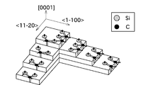
- the material of the base substrate may be SiC, and the off angle with respect to the ⁇ 11-20> direction or the ⁇ 1-100> direction may be 1 ° or less.
- the terrace is widened, and a high-quality SiC epitaxial layer is easily formed regardless of the crystal polymorph of the base substrate.
- the temperature gradient is 2 ° C./mm or less in the epitaxial layer growth step.
- the epitaxial layer can be sufficiently grown even with the low temperature gradient as described above. Therefore, the heating device or heating control can be simplified.
- the epitaxial layer growth step it is preferable that in the epitaxial layer growth step, a plurality of the underlying substrates are arranged in the SiC container, and the epitaxial layers are grown on each of the plurality of the underlying substrates.
- an epitaxial layer can be simultaneously formed on a plurality of base substrates, so that the processing can be made efficient.
- the epitaxial layer can be uniformly formed regardless of the position in the SiC container, so that the quality does not deteriorate.
- the inner surface of the TaC container is made of Si or Si compound, and by heating during the growth of the epitaxial layer, Si atoms are sublimated from the inner surface of the TaC container, so that the inside of the TaC container is Si vapor pressure is preferred.
- the crystal polymorph of the epitaxial layer is preferably 3C—SiC.
- the crystal polymorph of the epitaxial layer may be 4H—SiC or 6H—SiC.
- a method for manufacturing a substrate with an epitaxial layer using the vapor phase epitaxial growth method is provided.
- the material of the base substrate is SiC.
- the base substrate is accommodated in the TaC container without passing through the SiC container and heated under Si vapor pressure to etch the base substrate.
- the TaC container can be used not only at the time of forming the epitaxial layer but also at the time of etching.
- FIG. 3 is a schematic cross-sectional view showing a state in which a 3C—SiC epitaxial layer is simultaneously formed on a plurality of base substrates.
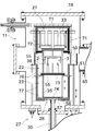
- FIG. 1 is a schematic diagram showing a high-temperature vacuum furnace 11 used for heat treatment.
- FIG. 2 is a cross-sectional view showing the main heating chamber and the preheating chamber of the high-temperature vacuum furnace 11 in detail.
- FIG. 3 is a schematic cross-sectional view showing a process of growing an epitaxial layer using the TaC container 2 and the SiC container 3.
- the high-temperature vacuum furnace 11 includes a main heating chamber 21 capable of heating an object to be processed (such as a base substrate) to a temperature of 1000 ° C. to 2300 ° C., and an object to be processed. And a preheating chamber 22 that can be preheated to a temperature of 500 ° C. or higher.
- the preheating chamber 22 is disposed below the main heating chamber 21 and is adjacent to the main heating chamber 21 in the vertical direction.
- the high-temperature vacuum furnace 11 includes a heat insulating chamber 23 disposed below the preheating chamber 22.
- the heat insulation chamber 23 is adjacent to the preheating chamber 22 in the vertical direction.
- the high-temperature vacuum furnace 11 includes a vacuum chamber 19, and the main heating chamber 21 and the preheating chamber 22 are provided inside the vacuum chamber 19.
- a turbo molecular pump 34 as a vacuum forming device is connected to the vacuum chamber 19 so that a vacuum of, for example, 10 ⁇ 2 Pa or less, preferably 10 ⁇ 7 Pa or less can be obtained in the vacuum chamber 19. Yes.
- a gate valve 25 is interposed between the turbo molecular pump 34 and the vacuum chamber 19. Further, an auxiliary rotary pump 26 is connected to the turbo molecular pump 34.
- the high-temperature vacuum furnace 11 includes a moving mechanism 27 that can move an object to be processed in the vertical direction between the preheating chamber 22 and the main heating chamber 21.
- the moving mechanism 27 includes a support body 28 that can support an object to be processed, and a cylinder portion 29 that can move the support body 28 up and down.
- the cylinder portion 29 includes a cylinder rod 30, and one end of the cylinder rod 30 is connected to the support body 28.
- the high-temperature vacuum furnace 11 is provided with a vacuum gauge 31 for measuring the degree of vacuum and a mass analyzer 32 for performing mass spectrometry.
- the vacuum chamber 19 is connected to a stock chamber (not shown) for storing an object to be processed through a transfer path 65.
- the transport path 65 can be opened and closed by a gate valve 66.
- the main heating chamber 21 is formed in a regular hexagonal shape in a plan sectional view and is disposed in the upper part of the internal space of the vacuum chamber 19. As shown in FIG. 2, a mesh heater 33 as a heater is provided inside the main heating chamber 21.
- a first multilayer heat reflecting metal plate 71 is fixed to the side wall or ceiling of the main heating chamber 21, and the heat of the mesh heater 33 is directed toward the center of the main heating chamber 21 by the first multilayer heat reflecting metal plate 71. It is configured to reflect.
- the mesh heater 33 is disposed so as to surround the workpiece to be heat-treated in the main heating chamber 21, and the multilayer heat-reflecting metal plate 71 is disposed on the outside thereof. Further, the mesh heater 33 is configured to increase in width toward the upper side, for example, or configured to increase the electric power supplied toward the upper side. Thereby, a temperature gradient can be provided in the main heating chamber 21.
- the main heating chamber 21 can be heated to a temperature of 1000 ° C. or higher and 2300 ° C. or lower, for example.
- the ceiling side of the main heating chamber 21 is closed by a first multilayer heat reflecting metal plate 71, while a through hole 55 is formed in the first multilayer heat reflecting metal plate 71 on the bottom surface.
- the object to be processed can move between the main heating chamber 21 and the preheating chamber 22 adjacent to the lower side of the main heating chamber 21 through the through hole 55.
- the support 28 has a configuration in which the second multilayer heat-reflecting metal plate 72, the third multilayer heat-reflecting metal plate 73, and the fourth multilayer heat-reflecting metal plate 74 are arranged at intervals from each other in order from the top. .
- the three multilayer heat-reflecting metal plates 72 to 74 are all arranged horizontally and are connected to each other by a column portion 35 provided in the vertical direction.
- the receiving stand 36 is arrange
- the TaC container 2 in which the to-be-processed object was accommodated on this receiving stand 36 is shown. It is configured so that it can be placed.
- the cradle 36 is made of tantalum carbide.
- a flange is formed at the end of the cylinder rod 30 of the cylinder portion 29, and this flange is fixed to the lower surface of the fourth multilayer heat reflecting metal plate 74.
- the preheating chamber 22 is configured by surrounding the lower space of the main heating chamber 21 with a multilayer heat reflecting metal plate 76.
- the preheating chamber 22 is configured to be circular in a plan sectional view. In the preheating chamber 22, no heating means such as the mesh heater 33 is provided.
- a through hole 56 is formed in the multilayer heat reflecting metal plate 76 at the bottom surface of the preheating chamber 22. Further, in the multilayer heat reflecting metal plate 76 that forms the side wall of the preheating chamber 22, a passage hole 50 is formed at a portion facing the transport path 65. Further, the high temperature vacuum furnace 11 includes an opening / closing member 51 capable of closing the passage hole 50.
- the heat insulating chamber 23 adjacent to the lower side of the preheating chamber 22 is partitioned on the upper side by the multilayer heat reflecting metal plate 76 and on the lower side and the side portion by the multilayer heat reflecting metal plate 77.
- a through-hole 57 is formed in the multilayer heat reflecting metal plate 77 covering the lower side of the heat insulation chamber 23 so that the cylinder rod 30 can be inserted.
- the multi-layer heat reflecting metal plate 77 is formed with a storage recess 58.
- the storage recess 58 can store a fourth multilayer heat-reflecting metal plate 74 included in the support 28.
- Each of the multilayer heat reflecting metal plates 71 to 74, 76, 77 has a structure in which metal plates (made of tungsten) are laminated at a predetermined interval. Also in the opening / closing member 51, a multilayer heat reflecting metal plate having the same configuration is used for a portion that closes the passage hole 50.
- any material can be used for the multilayer heat-reflecting metal plates 71 to 74, 76, and 77 as long as it has sufficient heating characteristics against the heat radiation of the mesh heater 33 and has a melting point higher than the ambient temperature.
- refractory metal materials such as tantalum, niobium, and molybdenum can be used as the multilayer heat reflecting metal plates 71 to 74, 76, and 77 in addition to the tungsten.
- carbides such as tungsten carbide, zirconium carbide, tantalum carbide, hafnium carbide, and molybdenum carbide can be used as the multilayer heat reflecting metal plates 71 to 74, 76, and 77.
- an infrared reflection film made of gold, tungsten carbide or the like may be further formed on the reflection surface.
- the multilayer heat-reflecting metal plates 72 to 74 provided in the support 28 have a structure in which tungsten plates having a punch metal structure having a large number of small through holes are laminated at predetermined intervals while different positions of the through holes are provided. It has become.
- the number of stacked second multilayer heat reflecting metal plates 72 provided in the uppermost layer of the support 28 is smaller than the number of stacked first multilayer heat reflecting metal plates 71 in the main heating chamber 21.
- the object to be processed is introduced into the vacuum chamber 19 from the conveyance path 65 and placed on the cradle 36 in the preheating chamber 22.
- the mesh heater 33 is driven in this state, the main heating chamber 21 is heated to a predetermined temperature (for example, about 1900 ° C.) between 1000 ° C. and 2300 ° C.
- the pressure in the vacuum chamber 19 is adjusted to 10 ⁇ 3 Pa or less, preferably 10 ⁇ 5 Pa or less by driving the turbo molecular pump 34.
- the number of laminated second multilayer heat reflecting metal plates 72 of the support 28 is smaller than the number of laminated first multilayer heat reflecting metal plates 71. Accordingly, part of the heat generated by the mesh heater 33 is appropriately supplied (distributed) to the preheating chamber 22 via the second multilayer heat reflecting metal plate 72, and the object to be processed in the preheating chamber 22 is heated to 500 ° C. or higher. Can be preheated to a predetermined temperature (for example, 800 ° C.). That is, preheating can be realized without installing a heater in the preheating chamber 22, and a simple structure of the preheating chamber 22 can be realized.
- a predetermined temperature for example, 800 ° C.
- the cylinder part 29 is driven and the support 28 is raised.
- the object to be processed passes through the through hole 55 from the lower side and moves into the main heating chamber 21.
- the main heat treatment is immediately started, and the object to be processed in the main heating chamber 21 can be rapidly heated to a predetermined temperature (about 1900 ° C.).
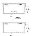
- the TaC container 2 is a fitting container provided with an upper container 2a and a lower container 2b that can be fitted to each other, as shown in FIG. With this configuration, the internal space of the TaC container 2 is sealed, but some gas atoms can move from the inside of the TaC container 2 to the outside (or vice versa). Further, the TaC container 2 is configured to exhibit a C atom adsorption ion pump function described later when high temperature processing is performed under vacuum. Specifically, the TaC container 2 is made of a tantalum metal and has a tantalum carbide layer. It is configured to be exposed to the internal space.
- a TaC layer is formed in the innermost layer (layer closest to the object to be processed), a Ta 2 C layer is formed outside the TaC layer, The tantalum metal as a base material is formed on the outside. Therefore, as long as the high temperature treatment is continued under vacuum as described above, the TaC container 2 has a function of continuously adsorbing and taking in carbon atoms from the surface of the tantalum carbide layer. In this sense, the TaC container 2 of this embodiment has a C atom adsorption ion pump function (ion getter function). Further, Si is added to the innermost TaC layer. Thereby, the Si sublimates during the heat treatment to generate Si vapor. And since only C vapor
- the Si supply source is not limited to the structure in which Si is applied to the inner wall of the TaC container 2.
- the inner wall of the TaC container 2 is made of Ta x Si y (for example, TaSi 2 or Ta 5 Si 3 ).
- other Si compounds may be used.
- solid Si Si pellet may be disposed inside the TaC container 2.
- the SiC container 3 includes polycrystalline SiC such as 3C-SiC.
- the entire SiC container 3 is made of SiC.
- a part (for example, the inner surface) of the SiC container 3 may be made of polycrystalline SiC.
- the SiC container 3 is a fitting container including an upper container 3a and a lower container 3b that can be fitted to each other, like the TaC container 2. With this configuration, the internal space of the SiC container 3 is sealed, but some gas atoms can move from the inside of the SiC container 3 to the outside (or vice versa). Thereby, the Si vapor generated inside the TaC container 2 can move from the outside to the inside of the SiC container 3 and can be supplied to the internal space of the SiC container 3.
- the SiC container 3 is smaller than the TaC container 2 because it is disposed inside the TaC container 2. Further, at least one base substrate 40 is accommodated in the SiC container 3.
- the base substrate 40 is a base or a base substrate for forming the epitaxial layer 41.
- the base substrate 40 may be a SiC substrate or a substrate made of a material other than SiC (for example, an Al compound or an N compound).
- the crystal polymorphism is arbitrary, and can be composed of, for example, 3C—SiC, 4H—SiC, or 6H—SiC.
- the off angle (see FIG. 5) with respect to the ⁇ 11-20> direction or the ⁇ 1-100> direction may be 1 ° or less, or may be larger than 1 °. good.
- the epitaxial layer 41 may be formed on either the Si surface or the C surface of the base substrate 40.
- an epitaxial layer 41 of single crystal 3C—SiC is formed on the base substrate 40 by a vapor phase epitaxial growth method.
- the base substrate 40 is accommodated in the SiC container 3, and the SiC container 3 is further accommodated in the TaC container 2.
- a temperature gradient is provided so that the upper side of the TaC container 2 (the side on which the epitaxial layer 41 is formed) becomes high temperature.
- the temperature gradient is preferably 2 ° C./mm or less, more preferably about 1 ° C./mm. In this state, the TaC container 2 is heated at a high temperature of 1600 ° C. or higher and 2300 ° C. or lower.
- Si applied to the inner surface of the TaC container 2 is sublimated, and the inside of the TaC container 2 becomes the equilibrium vapor pressure of Si.
- the inside of the TaC container 2 becomes the equilibrium vapor pressure of Si by sublimation of Si.
- the SiC container 3 is heated at a high temperature under the Si vapor pressure, the SiC container 3 is etched (Si vapor pressure etching). Specifically, the following reaction is performed. Briefly, when SiC is heated under Si vapor pressure, SiC is sublimated as Si 2 C or SiC 2 due to thermal decomposition and chemical reaction with Si.
- a high C partial pressure is generated inside the SiC container 3, and a C component is transported to the surface of the base substrate 40 with a temperature gradient of 2 ° C./mm or less as a driving force, so that 3C—SiC is crystallized.
- the SiC container 3 When the SiC container 3 is etched by Si vapor pressure, carbonization of the SiC container 3 can be prevented, and C atoms (or C compounds) can be sublimated from the SiC container 3.
- the TaC container 2 since the TaC container 2 has a C atom adsorption ion pump function as described above, the inside of the TaC container 2 and the outside of the SiC container 3 is a high-purity Si atmosphere. On the other hand, the inside of the SiC container 3 becomes a C atmosphere because C atoms are not absorbed. Further, Si vapor generated from the Si source of the TaC container 2 also enters the inside of the SiC container 3 through the gap between the upper container 3a and the lower container 3b of the SiC container 3.
- the inside of the SiC container 3 becomes an Si + C atmosphere. Therefore, by performing heat treatment while providing a temperature gradient, the single crystal 3C—SiC epitaxial layer 41 can be formed on the surface of the base substrate 40 (epitaxial layer growth step). Thereby, a substrate with an epitaxial layer can be manufactured.
- 3C—SiC is configured such that Si atoms and C atoms are stacked, and the height of the monomolecular layer made of Si and C is 0.25 nm.
- the arrangement direction of 4H—SiC is reversed every two molecular layers, while 3C—SiC is constant without reversing the arrangement direction.
- the partial pressure of the C vapor inside the SiC container 3 can be increased by covering the base substrate 40 with the TaC container 2 and the SiC container 3 as described above. Therefore, the epitaxial layer 41 can be sufficiently grown even when the temperature gradient is about 1 ° C./mm.
- a conventionally known sublimation method or the like requires a temperature gradient with a larger height difference in order to realize an effective growth rate.
- a precise heating device and fine control are required, which increases the manufacturing cost.
- the temperature gradient may be 2 ° C./mm or less, about 1 ° C./mm, or 1 ° C./mm or less, so that the manufacturing cost can be reduced.
- the single crystal 3C—SiC epitaxial layer 41 can be formed even if the base substrate 40 is other than SiC. Further, even if the base substrate 40 is other than 3C—SiC, the single crystal 3C—SiC epitaxial layer 41 can be formed. SiC can also be grown on 4H—SiC by performing MBE (molecular beam epitaxy) and CVD (chemical vapor deposition). However, the MBE method and the CVD method are unsuitable for heat treatment at a high temperature of 1600 ° C. or higher, for example, and therefore have an upper limit on the growth rate.
- MBE molecular beam epitaxy
- CVD chemical vapor deposition
- the proximity sublimation method can be expected to increase the growth temperature and increase the growth rate, but the uniformity in the substrate surface is a problem.
- the method of this embodiment is suitable for heat treatment at a high temperature of 1600 ° C. or higher, and the epitaxial growth of SiC is performed in a quasi-closed system called a Poly-SiC container, so that the uniformity is high.
- the off-angle of the SiC substrate is large (for example, greater than 1 °), step flow growth occurs, and it becomes easy to inherit the crystal polymorph of the base substrate 40. Therefore, the 4H—SiC that is the base substrate 40 is formed on the base substrate 40. Then, 4H—SiC as the epitaxial layer 41 grows. Therefore, when the 3C—SiC epitaxial layer 41 is required, it is preferable that the off-angle of the SiC substrate is small (for example, 1 ° or less).
- the SiC container 3 is disposed inside and outside the TaC container 2, and the epitaxial layer 41 is grown on the base substrate 40 inside each SiC container 3.
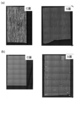
- FIG. 7A is a photomicrograph of the Si surface and the C surface of the epitaxial layer 41 when the SiC container 3 is disposed outside the TaC container 2 and epitaxially grown.
- FIG. 7B is a photomicrograph of the Si surface and the C surface of the epitaxial layer 41 when the SiC container 3 is disposed inside the TaC container 2 and epitaxially grown.
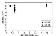
- the base substrate 40 was placed in various environments, heated at 1800 ° C. and a temperature gradient of about 1 ° C./mm, and the growth amounts of the epitaxial layers 41 were compared.
- the experiment was performed by changing the distance L from the surface of the base substrate 40 to the raw material (SiC container 3 or polycrystalline SiC plate 45).
- one base substrate 40 is accommodated in one SiC container 3.
- one SiC container 3 is stored. Two base substrates 40 are accommodated.
- the TaC container 2 is omitted, but each SiC container 3 is accommodated in the TaC container 2.
- FIG. 9 shows the distance L from the surface of the base substrate 40 to the raw material and the growth rate of the epitaxial layer 41 formed on the base substrate 40 for the base substrate 40 used in FIGS. 8A to 8D.
- the epitaxial layer 41 can be efficiently formed by housing a plurality of base substrates 40 in one SiC container 3.
- the growth rate of the epitaxial layer 41 is 6 to 8 ⁇ m / h at 1800 ° C., which is 6 to 8 times that of the CVD method of Patent Document 1.
- the heating temperature can be set to 1800 ° C. or higher, a higher growth rate can be realized.
- a higher growth rate can also be realized by making the temperature gradient larger than 1 ° C./mm.
- the TaC container 2 of the present embodiment can be used not only for the process of forming the epitaxial layer 41 but also for the process of etching the base substrate 40 (SiC substrate).
- SiC substrate the base substrate 40
- a SiC substrate is disposed directly on the TaC container 2 (without the SiC container 3).
- the SiC substrate can be etched (the above-described Si vapor pressure etching).
- etching may be performed to flatten the SiC substrate after being cut out from the ingot and mechanically polished (that is, before the formation of the epitaxial layer 41), or ions ( Etching may be performed to planarize the rough epitaxial layer 41 by implanting (impurities) (that is, after the epitaxial layer 41 is formed).
- the SiC container 3 is accommodated in the TaC container 2
- the base substrate 40 is accommodated in the SiC container 3, and vapor phase epitaxial growth is performed, whereby single crystal 3C—SiC is used as the epitaxial layer 41 to form the base substrate 40.
- the crystal polymorph of the epitaxial layer 41 to be grown can be selected by changing the off-angle and temperature of the base substrate 40.
- FIG. 11 shows an embodiment in which a plurality of base substrates 40 are accommodated in one SiC container 3 and accommodated in the TaC container 2.
- the single crystal 3C-SiC epitaxial layer 41 having the same growth rate and quality can be formed regardless of the position of the SiC container 3, so that the substrate with the epitaxial layer 41 is formed. It can be formed efficiently.
- the SiC container 3 made of a material containing polycrystalline SiC is housed in the TaC container 2 made of a material containing TaC, and the inside of the SiC container 3 is inside.
- the TaC container 2 is heated with a temperature gradient so that the inside of the TaC container 2 has a Si vapor pressure.
- C atoms sublimated by etching the inner surface of the SiC container 3 and Si atoms in the atmosphere inside the SiC container 3 are bonded to each other, so that single crystal SiC (3C— An epitaxial layer 41 of SiC, 4H—SiC, 6H—SiC, etc.) is grown.
- the high purity single crystal SiC epitaxial layer 41 can be formed at high speed. Moreover, since the raw material of the epitaxial layer 41 is the SiC container 3, the epitaxial layer 41 can be grown uniformly compared with CVD etc. which introduce
- the material of the base substrate 40 may be an Al compound or an N compound, and the material of the epitaxial layer 41 is SiC, in the ⁇ 11-20> direction or ⁇
- the off angle with respect to the 1-100> direction may be 1 ° or less.
- the base substrate 40 is not limited to SiC by using the method of the present invention, a highly versatile epitaxial growth method can be realized. Thereby, when the base substrate 40 is SiC and the off-angle is small, the terrace is widened, and an epitaxial layer of high-quality single crystal SiC is easily formed regardless of the crystal polymorph of the base substrate 40.
- the temperature gradient is 2 ° C./mm or less.
- the epitaxial layer can be sufficiently grown even with the low temperature difference as described above. Therefore, the heating device or heating control can be simplified.
- a plurality of base substrates 40 are arranged in the SiC container 3, and the epitaxial layer 41 is grown on each of the plurality of base substrates 40.
- the epitaxial layer 41 can be simultaneously formed on the plurality of base substrates 40, the processing can be made efficient.
- the epitaxial layer 41 can be uniformly formed regardless of the position in the SiC container 3 by using the method of the present invention, the quality does not deteriorate.
- the inner surface of the TaC container 2 is made of Si or Si compound, and by heating during the growth of the epitaxial layer 41, Si atoms are sublimated from the inner surface of the TaC container 2, The inside of the TaC container 2 is set to Si vapor pressure.
- the shapes of the TaC container 2 and the SiC container 3 described above are arbitrary and can be changed as appropriate.
- the TaC container 2 and the SiC container 3 may have different shapes or the same (similar) shape.
- the TaC container 2 or the SiC container 3 may have a plurality of spaces as shown in FIG.
- a plurality of SiC containers 3 may be accommodated in one TaC container 2, or a plurality of base substrates 40 may be accommodated in the SiC container 3 to form the epitaxial layer 41.
- an inert gas Ar gas or the like
- Ar gas Ar gas or the like
- the atmosphere in the internal space of the TaC container 2 and the internal space of the SiC container 3 is the amount of the Si source, the degree of TaC carbon adsorption function, the volume of the TaC container 2, and the volume of the SiC container 3. Therefore, the growth rate and quality of the epitaxial layer 41 can be controlled by making them different.
Abstract
Description
2a 上容器
2b 下容器
3 SiC容器
3a 上容器
3b 下容器
11 高温真空炉
40 SiC基板
41 エピタキシャル層
45 多結晶SiCプレート 2
Claims (10)
- TaCを含む材料で構成されるTaC容器の内部に、多結晶SiCを含む材料で構成されるSiC容器を収容し、当該SiC容器の内部に下地基板を収容した状態で、
当該TaC容器内がSi蒸気圧となるように、かつ、温度勾配を設けて前記TaC容器を加熱することで、
前記SiC容器の内面がエッチングされることで昇華したC原子と、雰囲気中のSi原子と、が結合することで、前記下地基板上に単結晶SiCのエピタキシャル層を成長させるエピタキシャル層成長工程を行うことを特徴とする気相エピタキシャル成長方法。 In a state where a SiC container made of a material containing polycrystalline SiC is housed inside a TaC container made of a material containing TaC, and a base substrate is housed inside the SiC container,
By heating the TaC container with a temperature gradient so that the inside of the TaC container has a Si vapor pressure,
An epitaxial layer growth step of growing an epitaxial layer of single-crystal SiC on the base substrate by combining C atoms sublimated by etching the inner surface of the SiC container and Si atoms in the atmosphere. A vapor phase epitaxial growth method characterized by the above. - 請求項1に記載の気相エピタキシャル成長方法であって、
前記下地基板の材料がAl化合物又はN化合物であることを特徴とする気相エピタキシャル成長方法。 The vapor phase epitaxial growth method according to claim 1,
A vapor phase epitaxial growth method, wherein the material of the base substrate is an Al compound or an N compound. - 請求項1に記載の気相エピタキシャル成長方法であって、
前記下地基板の材料がSiCであり、<11-20>方向又は<1-100>方向に対するオフ角が1°以下であることを特徴とする気相エピタキシャル成長方法。 The vapor phase epitaxial growth method according to claim 1,
A vapor phase epitaxial growth method characterized in that a material of the base substrate is SiC and an off angle with respect to the <11-20> direction or the <1-100> direction is 1 ° or less. - 請求項1に記載の気相エピタキシャル成長方法であって、
エピタキシャル層成長工程では、温度勾配が2℃/mm以下であることを特徴とする気相エピタキシャル成長方法。 The vapor phase epitaxial growth method according to claim 1,
A vapor phase epitaxial growth method characterized in that in the epitaxial layer growth step, the temperature gradient is 2 ° C./mm or less. - 請求項1に記載の気相エピタキシャル成長方法であって、
エピタキシャル層成長工程では、前記SiC容器に複数枚の前記下地基板を配置して、当該複数枚の前記下地基板のそれぞれに前記エピタキシャル層を成長させることを特徴とする気相エピタキシャル成長方法。 The vapor phase epitaxial growth method according to claim 1,
In the epitaxial layer growth step, a plurality of the underlying substrates are arranged in the SiC container, and the epitaxial layer is grown on each of the multiple underlying substrates. - 請求項1に記載の気相エピタキシャル成長方法であって、
前記TaC容器の内面をSi又はSi化合物とし、前記エピタキシャル層の成長時の加熱により、当該TaC容器の内面からSi原子が昇華することで、当該TaC容器内をSi蒸気圧とすることを特徴とする気相エピタキシャル成長方法。 The vapor phase epitaxial growth method according to claim 1,
The inner surface of the TaC container is made of Si or a Si compound, and Si atoms are sublimated from the inner surface of the TaC container by heating during the growth of the epitaxial layer, thereby making the inside of the TaC container have a Si vapor pressure. Vapor phase epitaxial growth method. - 請求項1に記載の気相エピタキシャル成長方法であって、
前記エピタキシャル層の結晶多形が3C-SiCであることを特徴とする気相エピタキシャル成長方法。 The vapor phase epitaxial growth method according to claim 1,
A vapor phase epitaxial growth method, wherein the crystal polymorph of the epitaxial layer is 3C-SiC. - 請求項1に記載の気相エピタキシャル成長方法であって、
前記エピタキシャル層の結晶多形が4H-SiC又は6H-SiCであることを特徴とする気相エピタキシャル成長方法。 The vapor phase epitaxial growth method according to claim 1,
A vapor phase epitaxial growth method, wherein the crystal polymorph of the epitaxial layer is 4H—SiC or 6H—SiC. - 請求項1に記載の気相エピタキシャル成長方法を用いることを特徴とするエピタキシャル層付き基板の製造方法。 A method for producing a substrate with an epitaxial layer, wherein the vapor phase epitaxial growth method according to claim 1 is used.
- 請求項9に記載のエピタキシャル層付き基板の製造方法であって、
前記下地基板の材料はSiCであり、前記下地基板をSiC容器を介さず前記TaC容器に収容してSi蒸気圧下で加熱することで当該下地基板をエッチングすることを特徴とするエピタキシャル層付き基板の製造方法。 It is a manufacturing method of the substrate with an epitaxial layer according to claim 9,
The material of the base substrate is SiC, the base substrate is accommodated in the TaC container without passing through the SiC container, and the base substrate is etched by heating under Si vapor pressure. Production method.
Priority Applications (11)
| Application Number | Priority Date | Filing Date | Title |
|---|---|---|---|
| EP17789663.6A EP3450595B1 (en) | 2016-04-28 | 2017-04-27 | Vapour-phase epitaxial growth method, and method for producing substrate equipped with epitaxial layer |
| CN202111339283.9A CN114351248A (en) | 2016-04-28 | 2017-04-27 | Vapor phase epitaxial growth method and preparation method of substrate with epitaxial layer |
| JP2018514703A JP6721904B2 (en) | 2016-04-28 | 2017-04-27 | Vapor phase epitaxial growth method and method for manufacturing substrate with epitaxial layer |
| EP21176448.5A EP3892761A1 (en) | 2016-04-28 | 2017-04-27 | Vapour-phase epitaxial growth method, and method for producing substrate equipped with epitaxial layer |
| CN201780026022.7A CN109072478B (en) | 2016-04-28 | 2017-04-27 | Vapor phase epitaxial growth method and preparation method of substrate with epitaxial layer |
| EP21176449.3A EP3892762A1 (en) | 2016-04-28 | 2017-04-27 | Vapour-phase epitaxial growth method, and method for producing substrate equipped with epitaxial layer |
| US16/096,475 US11359307B2 (en) | 2016-04-28 | 2017-04-27 | Vapour-phase epitaxial growth method, and method for producing substrate equipped with epitaxial layer |
| CN202111338480.9A CN114293247A (en) | 2016-04-28 | 2017-04-27 | Vapor phase epitaxial growth method and preparation method of substrate with epitaxial layer |
| US17/734,578 US20220259760A1 (en) | 2016-04-28 | 2022-05-02 | Manufacturing device for sic semiconductor substrate |
| US17/734,511 US20220259759A1 (en) | 2016-04-28 | 2022-05-02 | Container made of sic |
| US18/380,897 US20240044042A1 (en) | 2016-04-28 | 2023-10-17 | Method of using sic container |
Applications Claiming Priority (2)
| Application Number | Priority Date | Filing Date | Title |
|---|---|---|---|
| JP2016-092073 | 2016-04-28 | ||
| JP2016092073 | 2016-04-28 |
Related Child Applications (3)
| Application Number | Title | Priority Date | Filing Date |
|---|---|---|---|
| US16/096,475 A-371-Of-International US11359307B2 (en) | 2016-04-28 | 2017-04-27 | Vapour-phase epitaxial growth method, and method for producing substrate equipped with epitaxial layer |
| US17/734,578 Division US20220259760A1 (en) | 2016-04-28 | 2022-05-02 | Manufacturing device for sic semiconductor substrate |
| US17/734,511 Division US20220259759A1 (en) | 2016-04-28 | 2022-05-02 | Container made of sic |
Publications (1)
| Publication Number | Publication Date |
|---|---|
| WO2017188381A1 true WO2017188381A1 (en) | 2017-11-02 |
Family
ID=60159696
Family Applications (1)
| Application Number | Title | Priority Date | Filing Date |
|---|---|---|---|
| PCT/JP2017/016738 WO2017188381A1 (en) | 2016-04-28 | 2017-04-27 | Vapour-phase epitaxial growth method, and method for producing substrate equipped with epitaxial layer |
Country Status (5)
| Country | Link |
|---|---|
| US (4) | US11359307B2 (en) |
| EP (3) | EP3892762A1 (en) |
| JP (3) | JP6721904B2 (en) |
| CN (3) | CN114351248A (en) |
| WO (1) | WO2017188381A1 (en) |
Cited By (19)
| Publication number | Priority date | Publication date | Assignee | Title |
|---|---|---|---|---|
| WO2020095872A1 (en) * | 2018-11-05 | 2020-05-14 | 学校法人関西学院 | Sic semiconductor substrate, method for manufacturing same, and device for manufacturing same |
| WO2020095873A1 (en) * | 2018-11-05 | 2020-05-14 | 学校法人関西学院 | Sic semiconductor substrate, and, production method therefor and production device therefor |
| JP2020092113A (en) * | 2018-12-03 | 2020-06-11 | 昭和電工株式会社 | SiC CHEMICAL VAPOR DEPOSITION APPARATUS AND MANUFACTURING METHOD OF SiC EPITAXIAL WAFER |
| JPWO2020179793A1 (en) * | 2019-03-05 | 2020-09-10 | ||
| JPWO2020179794A1 (en) * | 2019-03-05 | 2020-09-10 | ||
| WO2020203517A1 (en) * | 2019-03-29 | 2020-10-08 | 学校法人関西学院 | Semiconductor substrate manufacturing device applicable to large-diameter semiconductor substrate |
| WO2020203516A1 (en) * | 2019-03-29 | 2020-10-08 | 学校法人関西学院 | Device for manufacturing semiconductor substrate comprising temperature gradient inversion means and method for manufacturing semiconductor substrate |
| WO2020218482A1 (en) * | 2019-04-26 | 2020-10-29 | 学校法人関西学院 | Method for manufacturing sic substrate, manufacturing device for same, and method for epitaxial growth |
| WO2020218483A1 (en) * | 2019-04-26 | 2020-10-29 | 学校法人関西学院 | Method of manufacturing semiconductor substrate, manufacturing apparatus therefor, and epitaxial growth method |
| WO2021025084A1 (en) * | 2019-08-06 | 2021-02-11 | 学校法人関西学院 | SiC SEED CRYSTAL AND METHOD FOR PRODUCING SAME, SiC INGOT PRODUCED BY GROWING SAID SiC SEED CRYSTAL AND METHOD FOR PRODUCING SAME, AND SiC WAFER PRODUCED FROM SAID SiC INGOT AND SiC WAFER WITH EPITAXIAL FILM AND METHODS RESPECTIVELY FOR PRODUCING SAID SiC WAFER AND SAID SiC WAFER WITH EPITAXIAL FILM |
| WO2021025086A1 (en) * | 2019-08-06 | 2021-02-11 | 学校法人関西学院 | SiC SUBSTRATE PRODUCTION METHOD |
| WO2021025077A1 (en) * | 2019-08-06 | 2021-02-11 | 株式会社デンソー | METHOD FOR MANUFACTURING SiC SUBSTRATE |
| WO2021060365A1 (en) * | 2019-09-27 | 2021-04-01 | 学校法人関西学院 | Method for producing semiconductor substrates and device for producing semiconductor substrates |
| WO2021060366A1 (en) * | 2019-09-27 | 2021-04-01 | 学校法人関西学院 | Method of manufacturing sic semiconductor device and sic semiconductor device |
| WO2021060368A1 (en) * | 2019-09-27 | 2021-04-01 | 学校法人関西学院 | Sic single crystal manufacturing method, sic single crystal manufacturing device, and sic single crystal wafer |
| WO2021060367A1 (en) * | 2019-09-27 | 2021-04-01 | 学校法人関西学院 | Method for manufacturing sic substrate |
| JP2022039876A (en) * | 2020-08-28 | 2022-03-10 | 李輝雄 | Organic material cracker and organic material cracking method |
| CN114174567A (en) * | 2019-03-05 | 2022-03-11 | 学校法人关西学院 | Method and apparatus for manufacturing SiC substrate |
| TWI833919B (en) | 2019-03-05 | 2024-03-01 | 學校法人關西學院 | Silicon carbide substrate, method for manufacturing silicon carbide substrate, device for manufacturing silicon carbide substrate, and method for reducing processing-degraded layer of silicon carbide substrate |
Families Citing this family (3)
| Publication number | Priority date | Publication date | Assignee | Title |
|---|---|---|---|---|
| CN114351248A (en) * | 2016-04-28 | 2022-04-15 | 学校法人关西学院 | Vapor phase epitaxial growth method and preparation method of substrate with epitaxial layer |
| CN113078047A (en) * | 2021-03-30 | 2021-07-06 | 芜湖启迪半导体有限公司 | Bonded Si substrate, preparation method thereof, and method for preparing Si/3C-SiC heterostructure and 3C-SiC film |
| CN114373972A (en) * | 2022-01-14 | 2022-04-19 | 东莞富瑟尔科技有限公司 | Molten salt diffusion compounding device and method |
Citations (3)
| Publication number | Priority date | Publication date | Assignee | Title |
|---|---|---|---|---|
| JP2009007193A (en) * | 2007-06-27 | 2009-01-15 | Kwansei Gakuin | Heat treatment apparatus and heat treatment method |
| JP2010064919A (en) * | 2008-09-10 | 2010-03-25 | Showa Denko Kk | Method for annealing silicon carbide single crystal material, silicon carbide single crystal wafer, and silicon carbide semiconductor |
| JP2013189323A (en) * | 2012-03-12 | 2013-09-26 | Sumitomo Electric Ind Ltd | Method for manufacturing silicon carbide single crystal |
Family Cites Families (24)
| Publication number | Priority date | Publication date | Assignee | Title |
|---|---|---|---|---|
| GB1458445A (en) * | 1974-02-21 | 1976-12-15 | Fiz Tekh Inst Ioffe | Method of producing epitaxial deposits of semiconductor silicon carbide |
| US4649002A (en) * | 1985-04-01 | 1987-03-10 | Kennecott Corporation | System for preventing decomposition of silicon carbide articles during sintering |
| US5679153A (en) | 1994-11-30 | 1997-10-21 | Cree Research, Inc. | Method for reducing micropipe formation in the epitaxial growth of silicon carbide and resulting silicon carbide structures |
| DE59506491D1 (en) | 1994-12-01 | 1999-09-02 | Siemens Ag | METHOD AND DEVICE FOR PRODUCING SILICON CARBIDE CRYSTALS BY SUBLIMATION BREEDING |
| US5989340A (en) * | 1995-11-14 | 1999-11-23 | Siemens Aktiengesellschaft | Process and device for sublimation growing of silicon carbide monocrystals |
| JP3550967B2 (en) * | 1997-09-11 | 2004-08-04 | 富士電機ホールディングス株式会社 | Heat treatment method for silicon carbide substrate |
| EP1026290B1 (en) | 1997-09-12 | 2009-08-26 | Showa Denko Kabushiki Kaisha | Method and apparatus for producing silicon carbide single crystal |
| JP2981879B2 (en) * | 1998-03-06 | 1999-11-22 | 日本ピラー工業株式会社 | Single crystal SiC and method for producing the same |
| JP4482642B2 (en) * | 2003-10-21 | 2010-06-16 | 学校法人関西学院 | Single crystal silicon carbide growth method |
| JP4035136B2 (en) * | 2004-02-04 | 2008-01-16 | 松下電器産業株式会社 | Method for fixing seed crystal and method for producing single crystal using the fixing method |
| US7323052B2 (en) * | 2005-03-24 | 2008-01-29 | Cree, Inc. | Apparatus and method for the production of bulk silicon carbide single crystals |
| JP4954593B2 (en) | 2006-04-18 | 2012-06-20 | 新日本製鐵株式会社 | Epitaxial silicon carbide single crystal substrate manufacturing method, and device using the obtained epitaxial silicon carbide single crystal substrate |
| ITMI20062213A1 (en) * | 2006-11-20 | 2008-05-21 | Lpe Spa | REACTOR TO GROW CRYSTALS |
| JP4521588B2 (en) * | 2007-12-25 | 2010-08-11 | 株式会社エコトロン | Method for producing single crystal SiC film |
| JP5564682B2 (en) * | 2010-04-28 | 2014-07-30 | 学校法人関西学院 | Manufacturing method of semiconductor device |
| JP2011243619A (en) * | 2010-05-14 | 2011-12-01 | Sumitomo Electric Ind Ltd | Manufacturing method of silicon carbide substrate, manufacturing method of semiconductor device, and silicon carbide substrate and semiconductor device |
| JP5561676B2 (en) * | 2010-07-21 | 2014-07-30 | 学校法人関西学院 | SiC semiconductor wafer heat treatment equipment |
| TWI600081B (en) * | 2012-11-16 | 2017-09-21 | Toyo Tanso Co Ltd | Surface treatment method of single crystal silicon carbide substrate and single crystal silicon carbide substrate |
| JP6093154B2 (en) * | 2012-11-16 | 2017-03-08 | 東洋炭素株式会社 | Method for manufacturing container |
| US8940614B2 (en) * | 2013-03-15 | 2015-01-27 | Dow Corning Corporation | SiC substrate with SiC epitaxial film |
| JP6226648B2 (en) * | 2013-09-04 | 2017-11-08 | 昭和電工株式会社 | Method for manufacturing SiC epitaxial wafer |
| US10753010B2 (en) * | 2014-09-25 | 2020-08-25 | Pallidus, Inc. | Vapor deposition apparatus and techniques using high puritiy polymer derived silicon carbide |
| JP2017105697A (en) * | 2015-11-26 | 2017-06-15 | 東洋炭素株式会社 | PRODUCTION METHOD OF THIN SiC WAFER, AND THIN SiC WAFER |
| CN114351248A (en) | 2016-04-28 | 2022-04-15 | 学校法人关西学院 | Vapor phase epitaxial growth method and preparation method of substrate with epitaxial layer |
-
2017
- 2017-04-27 CN CN202111339283.9A patent/CN114351248A/en active Pending
- 2017-04-27 EP EP21176449.3A patent/EP3892762A1/en active Pending
- 2017-04-27 CN CN201780026022.7A patent/CN109072478B/en active Active
- 2017-04-27 US US16/096,475 patent/US11359307B2/en active Active
- 2017-04-27 WO PCT/JP2017/016738 patent/WO2017188381A1/en active Application Filing
- 2017-04-27 EP EP21176448.5A patent/EP3892761A1/en active Pending
- 2017-04-27 JP JP2018514703A patent/JP6721904B2/en active Active
- 2017-04-27 CN CN202111338480.9A patent/CN114293247A/en active Pending
- 2017-04-27 EP EP17789663.6A patent/EP3450595B1/en active Active
-
2020
- 2020-06-09 JP JP2020099759A patent/JP6980202B2/en active Active
- 2020-06-09 JP JP2020099758A patent/JP6980201B2/en active Active
-
2022
- 2022-05-02 US US17/734,578 patent/US20220259760A1/en active Pending
- 2022-05-02 US US17/734,511 patent/US20220259759A1/en not_active Abandoned
-
2023
- 2023-10-17 US US18/380,897 patent/US20240044042A1/en active Pending
Patent Citations (3)
| Publication number | Priority date | Publication date | Assignee | Title |
|---|---|---|---|---|
| JP2009007193A (en) * | 2007-06-27 | 2009-01-15 | Kwansei Gakuin | Heat treatment apparatus and heat treatment method |
| JP2010064919A (en) * | 2008-09-10 | 2010-03-25 | Showa Denko Kk | Method for annealing silicon carbide single crystal material, silicon carbide single crystal wafer, and silicon carbide semiconductor |
| JP2013189323A (en) * | 2012-03-12 | 2013-09-26 | Sumitomo Electric Ind Ltd | Method for manufacturing silicon carbide single crystal |
Non-Patent Citations (1)
| Title |
|---|
| See also references of EP3450595A4 * |
Cited By (50)
| Publication number | Priority date | Publication date | Assignee | Title |
|---|---|---|---|---|
| WO2020095872A1 (en) * | 2018-11-05 | 2020-05-14 | 学校法人関西学院 | Sic semiconductor substrate, method for manufacturing same, and device for manufacturing same |
| EP3879010A4 (en) * | 2018-11-05 | 2022-07-13 | Kwansei Gakuin Educational Foundation | Sic semiconductor substrate, and, production method therefor and production device therefor |
| CN113227465A (en) * | 2018-11-05 | 2021-08-06 | 学校法人关西学院 | SiC semiconductor substrate, and method and apparatus for manufacturing same |
| JP7464806B2 (en) | 2018-11-05 | 2024-04-10 | 学校法人関西学院 | SiC semiconductor substrate, its manufacturing method and manufacturing device |
| CN113227465B (en) * | 2018-11-05 | 2024-03-29 | 学校法人关西学院 | SiC semiconductor substrate, and method and apparatus for manufacturing the same |
| JP7278550B2 (en) | 2018-11-05 | 2023-05-22 | 学校法人関西学院 | SiC semiconductor substrate, its manufacturing method, and its manufacturing apparatus |
| WO2020095873A1 (en) * | 2018-11-05 | 2020-05-14 | 学校法人関西学院 | Sic semiconductor substrate, and, production method therefor and production device therefor |
| JPWO2020095872A1 (en) * | 2018-11-05 | 2021-09-24 | 学校法人関西学院 | SiC semiconductor substrate, its manufacturing method, and its manufacturing equipment |
| US20210399095A1 (en) * | 2018-11-05 | 2021-12-23 | Kwansei Gakuin Educational Foundation | Sic semiconductor substrate, and, production method therefor and production device therefor |
| CN113227466A (en) * | 2018-11-05 | 2021-08-06 | 学校法人关西学院 | SiC semiconductor substrate, and method and apparatus for manufacturing same |
| EP3879011A4 (en) * | 2018-11-05 | 2022-07-20 | Kwansei Gakuin Educational Foundation | Sic semiconductor substrate, method for manufacturing same, and device for manufacturing same |
| JPWO2020095873A1 (en) * | 2018-11-05 | 2021-10-07 | 学校法人関西学院 | SiC semiconductor substrate, its manufacturing method, and its manufacturing equipment |
| JP7242990B2 (en) | 2018-12-03 | 2023-03-22 | 株式会社レゾナック | SiC chemical vapor deposition apparatus and method for manufacturing SiC epitaxial wafer |
| JP2020092113A (en) * | 2018-12-03 | 2020-06-11 | 昭和電工株式会社 | SiC CHEMICAL VAPOR DEPOSITION APPARATUS AND MANUFACTURING METHOD OF SiC EPITAXIAL WAFER |
| CN114207195A (en) * | 2019-03-05 | 2022-03-18 | 学校法人关西学院 | Method and apparatus for manufacturing SiC substrate and method for reducing macro-step bunching of SiC substrate |
| TWI824118B (en) * | 2019-03-05 | 2023-12-01 | 學校法人關西學院 | Silicon carbide epitaxial substrate, manufacturing method of silicon carbide epitaxial substrate, and manufacturing device of silicon carbide epitaxial substrate |
| US11972949B2 (en) | 2019-03-05 | 2024-04-30 | Kwansei Gakuin Educational Foundation | SiC substrate manufacturing method and manufacturing device, and method for reducing work-affected layer in sic substrate |
| JPWO2020179793A1 (en) * | 2019-03-05 | 2020-09-10 | ||
| JP7464807B2 (en) | 2019-03-05 | 2024-04-10 | 学校法人関西学院 | Method and apparatus for manufacturing SiC substrate, and method for reducing macro-step bunching of SiC substrate |
| JP7464808B2 (en) | 2019-03-05 | 2024-04-10 | 学校法人関西学院 | Method and apparatus for manufacturing SiC substrate, and method for reducing process-affected layer of SiC substrate |
| JPWO2020179794A1 (en) * | 2019-03-05 | 2020-09-10 | ||
| TWI833919B (en) | 2019-03-05 | 2024-03-01 | 學校法人關西學院 | Silicon carbide substrate, method for manufacturing silicon carbide substrate, device for manufacturing silicon carbide substrate, and method for reducing processing-degraded layer of silicon carbide substrate |
| CN114174567B (en) * | 2019-03-05 | 2023-12-15 | 学校法人关西学院 | Method and apparatus for manufacturing SiC substrate |
| CN114174567A (en) * | 2019-03-05 | 2022-03-11 | 学校法人关西学院 | Method and apparatus for manufacturing SiC substrate |
| EP4209626A1 (en) * | 2019-03-05 | 2023-07-12 | Kwansei Gakuin Educational Foundation | Sic epitaxial substrate manufacturing method and manufacturing device therefor |
| EP3936644A4 (en) * | 2019-03-05 | 2023-03-22 | Kwansei Gakuin Educational Foundation | Sic epitaxial substrate manufacturing method and manufacturing device therefor |
| US20220178048A1 (en) * | 2019-03-05 | 2022-06-09 | Kwansei Gakuin Educational Foundation | METHOD AND APPARATUS FOR PRODUCING SiC SUBSTRATE |
| EP3936646A4 (en) * | 2019-03-05 | 2023-01-04 | Kwansei Gakuin Educational Foundation | Sic substrate manufacturing method and manufacturing device, and method for reducing work-affected layer in sic substrate |
| EP3936643A4 (en) * | 2019-03-05 | 2022-11-09 | Kwansei Gakuin Educational Foundation | Method and apparatus for producing sic substrate |
| EP3936645A4 (en) * | 2019-03-05 | 2022-11-09 | Kwansei Gakuin Educational Foundation | Method and device for manufacturing sic substrate, and method for reducing macro-step bunching of sic substrate |
| WO2020203516A1 (en) * | 2019-03-29 | 2020-10-08 | 学校法人関西学院 | Device for manufacturing semiconductor substrate comprising temperature gradient inversion means and method for manufacturing semiconductor substrate |
| US11955354B2 (en) | 2019-03-29 | 2024-04-09 | Kwansei Gakuin Educational Foundation | Semiconductor substrate manufacturing device applicable to large-diameter semiconductor substrate |
| WO2020203517A1 (en) * | 2019-03-29 | 2020-10-08 | 学校法人関西学院 | Semiconductor substrate manufacturing device applicable to large-diameter semiconductor substrate |
| CN114174563A (en) * | 2019-04-26 | 2022-03-11 | 学校法人关西学院 | Method for manufacturing SiC substrate, apparatus for manufacturing the same, and epitaxial growth method |
| US11952678B2 (en) | 2019-04-26 | 2024-04-09 | Kwansei Gakuin Educational Foundation | Method for manufacturing etched SiC substrate and grown SiC substrate by material tranportation and method for epitaxial growth by material transportation |
| WO2020218483A1 (en) * | 2019-04-26 | 2020-10-29 | 学校法人関西学院 | Method of manufacturing semiconductor substrate, manufacturing apparatus therefor, and epitaxial growth method |
| WO2020218482A1 (en) * | 2019-04-26 | 2020-10-29 | 学校法人関西学院 | Method for manufacturing sic substrate, manufacturing device for same, and method for epitaxial growth |
| WO2021025077A1 (en) * | 2019-08-06 | 2021-02-11 | 株式会社デンソー | METHOD FOR MANUFACTURING SiC SUBSTRATE |
| WO2021025084A1 (en) * | 2019-08-06 | 2021-02-11 | 学校法人関西学院 | SiC SEED CRYSTAL AND METHOD FOR PRODUCING SAME, SiC INGOT PRODUCED BY GROWING SAID SiC SEED CRYSTAL AND METHOD FOR PRODUCING SAME, AND SiC WAFER PRODUCED FROM SAID SiC INGOT AND SiC WAFER WITH EPITAXIAL FILM AND METHODS RESPECTIVELY FOR PRODUCING SAID SiC WAFER AND SAID SiC WAFER WITH EPITAXIAL FILM |
| WO2021025086A1 (en) * | 2019-08-06 | 2021-02-11 | 学校法人関西学院 | SiC SUBSTRATE PRODUCTION METHOD |
| US20220290324A1 (en) * | 2019-08-06 | 2022-09-15 | Kwansei Gakuin Educational Foundation | SiC SUBSTRATE PRODUCTION METHOD |
| WO2021060367A1 (en) * | 2019-09-27 | 2021-04-01 | 学校法人関西学院 | Method for manufacturing sic substrate |
| US20220316089A1 (en) * | 2019-09-27 | 2022-10-06 | Kwansei Gakuin Educational Foundation | Method for producing semiconductor substrates and device for producing semiconductor substrates |
| US11932967B2 (en) | 2019-09-27 | 2024-03-19 | Kwansei Gakuin Educational Foundation | SiC single crystal manufacturing method, SiC single crystal manufacturing device, and SiC single crystal wafer |
| US20220344152A1 (en) * | 2019-09-27 | 2022-10-27 | Kwansei Gakuin Educational Foundation | Method for manufacturing sic substrate |
| CN114423890A (en) * | 2019-09-27 | 2022-04-29 | 学校法人关西学院 | Method for manufacturing SiC semiconductor device and SiC semiconductor device |
| WO2021060365A1 (en) * | 2019-09-27 | 2021-04-01 | 学校法人関西学院 | Method for producing semiconductor substrates and device for producing semiconductor substrates |
| WO2021060366A1 (en) * | 2019-09-27 | 2021-04-01 | 学校法人関西学院 | Method of manufacturing sic semiconductor device and sic semiconductor device |
| WO2021060368A1 (en) * | 2019-09-27 | 2021-04-01 | 学校法人関西学院 | Sic single crystal manufacturing method, sic single crystal manufacturing device, and sic single crystal wafer |
| JP2022039876A (en) * | 2020-08-28 | 2022-03-10 | 李輝雄 | Organic material cracker and organic material cracking method |
Also Published As
| Publication number | Publication date |
|---|---|
| EP3892761A1 (en) | 2021-10-13 |
| EP3450595A4 (en) | 2019-12-04 |
| US20190136409A1 (en) | 2019-05-09 |
| JP6721904B2 (en) | 2020-07-15 |
| JPWO2017188381A1 (en) | 2019-03-07 |
| EP3892762A1 (en) | 2021-10-13 |
| CN109072478B (en) | 2021-12-03 |
| US20220259760A1 (en) | 2022-08-18 |
| JP6980202B2 (en) | 2021-12-15 |
| EP3450595A1 (en) | 2019-03-06 |
| JP6980201B2 (en) | 2021-12-15 |
| JP2020169120A (en) | 2020-10-15 |
| CN109072478A (en) | 2018-12-21 |
| JP2020147499A (en) | 2020-09-17 |
| CN114351248A (en) | 2022-04-15 |
| US20240044042A1 (en) | 2024-02-08 |
| CN114293247A (en) | 2022-04-08 |
| US11359307B2 (en) | 2022-06-14 |
| EP3450595B1 (en) | 2021-07-14 |
| US20220259759A1 (en) | 2022-08-18 |
Similar Documents
| Publication | Publication Date | Title |
|---|---|---|
| JP6980202B2 (en) | SiC container | |
| JP6311834B2 (en) | Manufacturing method of nitride semiconductor substrate | |
| JP5464544B2 (en) | Single crystal SiC substrate with epitaxial growth layer, carbon supply feed substrate, and SiC substrate with carbon nanomaterial | |
| JP5360639B2 (en) | Surface modified single crystal SiC substrate, single crystal SiC substrate with epitaxial growth layer, semiconductor chip, seed substrate for single crystal SiC growth, and method for producing polycrystalline SiC substrate with single crystal growth layer | |
| JP5540349B2 (en) | Manufacturing method of semiconductor wafer | |
| KR101910696B1 (en) | Semiconductor wafer manufacturing method, and semiconductor wafer | |
| JP4431643B2 (en) | Single crystal silicon carbide growth method | |
| JP4482642B2 (en) | Single crystal silicon carbide growth method | |
| JP5688780B2 (en) | SiC substrate, carbon supply feed substrate, and SiC substrate with carbon nanomaterial | |
| JP5164121B2 (en) | Single crystal silicon carbide growth method |
Legal Events
| Date | Code | Title | Description |
|---|---|---|---|
| ENP | Entry into the national phase |
Ref document number: 2018514703 Country of ref document: JP Kind code of ref document: A |
|
| NENP | Non-entry into the national phase |
Ref country code: DE |
|
| 121 | Ep: the epo has been informed by wipo that ep was designated in this application |
Ref document number: 17789663 Country of ref document: EP Kind code of ref document: A1 |
|
| WWE | Wipo information: entry into national phase |
Ref document number: 2017789663 Country of ref document: EP |
|
| ENP | Entry into the national phase |
Ref document number: 2017789663 Country of ref document: EP Effective date: 20181128 |